US8013813B2 - Active matrix-type display device - Google Patents
Active matrix-type display device Download PDFInfo
- Publication number
- US8013813B2 US8013813B2 US12/064,091 US6409106A US8013813B2 US 8013813 B2 US8013813 B2 US 8013813B2 US 6409106 A US6409106 A US 6409106A US 8013813 B2 US8013813 B2 US 8013813B2
- Authority
- US
- United States
- Prior art keywords
- light emitting
- subframe
- subframes
- driver element
- voltage
- Prior art date
- Legal status (The legal status is an assumption and is not a legal conclusion. Google has not performed a legal analysis and makes no representation as to the accuracy of the status listed.)
- Active, expires
Links
Images


Classifications
-
- G—PHYSICS
- G09—EDUCATION; CRYPTOGRAPHY; DISPLAY; ADVERTISING; SEALS
- G09G—ARRANGEMENTS OR CIRCUITS FOR CONTROL OF INDICATING DEVICES USING STATIC MEANS TO PRESENT VARIABLE INFORMATION
- G09G3/00—Control arrangements or circuits, of interest only in connection with visual indicators other than cathode-ray tubes
- G09G3/20—Control arrangements or circuits, of interest only in connection with visual indicators other than cathode-ray tubes for presentation of an assembly of a number of characters, e.g. a page, by composing the assembly by combination of individual elements arranged in a matrix no fixed position being assigned to or needed to be assigned to the individual characters or partial characters
- G09G3/22—Control arrangements or circuits, of interest only in connection with visual indicators other than cathode-ray tubes for presentation of an assembly of a number of characters, e.g. a page, by composing the assembly by combination of individual elements arranged in a matrix no fixed position being assigned to or needed to be assigned to the individual characters or partial characters using controlled light sources
- G09G3/30—Control arrangements or circuits, of interest only in connection with visual indicators other than cathode-ray tubes for presentation of an assembly of a number of characters, e.g. a page, by composing the assembly by combination of individual elements arranged in a matrix no fixed position being assigned to or needed to be assigned to the individual characters or partial characters using controlled light sources using electroluminescent panels
- G09G3/32—Control arrangements or circuits, of interest only in connection with visual indicators other than cathode-ray tubes for presentation of an assembly of a number of characters, e.g. a page, by composing the assembly by combination of individual elements arranged in a matrix no fixed position being assigned to or needed to be assigned to the individual characters or partial characters using controlled light sources using electroluminescent panels semiconductive, e.g. using light-emitting diodes [LED]
- G09G3/3208—Control arrangements or circuits, of interest only in connection with visual indicators other than cathode-ray tubes for presentation of an assembly of a number of characters, e.g. a page, by composing the assembly by combination of individual elements arranged in a matrix no fixed position being assigned to or needed to be assigned to the individual characters or partial characters using controlled light sources using electroluminescent panels semiconductive, e.g. using light-emitting diodes [LED] organic, e.g. using organic light-emitting diodes [OLED]
- G09G3/3225—Control arrangements or circuits, of interest only in connection with visual indicators other than cathode-ray tubes for presentation of an assembly of a number of characters, e.g. a page, by composing the assembly by combination of individual elements arranged in a matrix no fixed position being assigned to or needed to be assigned to the individual characters or partial characters using controlled light sources using electroluminescent panels semiconductive, e.g. using light-emitting diodes [LED] organic, e.g. using organic light-emitting diodes [OLED] using an active matrix
- G09G3/3258—Control arrangements or circuits, of interest only in connection with visual indicators other than cathode-ray tubes for presentation of an assembly of a number of characters, e.g. a page, by composing the assembly by combination of individual elements arranged in a matrix no fixed position being assigned to or needed to be assigned to the individual characters or partial characters using controlled light sources using electroluminescent panels semiconductive, e.g. using light-emitting diodes [LED] organic, e.g. using organic light-emitting diodes [OLED] using an active matrix with pixel circuitry controlling the voltage across the light-emitting element
-
- G—PHYSICS
- G09—EDUCATION; CRYPTOGRAPHY; DISPLAY; ADVERTISING; SEALS
- G09G—ARRANGEMENTS OR CIRCUITS FOR CONTROL OF INDICATING DEVICES USING STATIC MEANS TO PRESENT VARIABLE INFORMATION
- G09G2300/00—Aspects of the constitution of display devices
- G09G2300/08—Active matrix structure, i.e. with use of active elements, inclusive of non-linear two terminal elements, in the pixels together with light emitting or modulating elements
- G09G2300/0809—Several active elements per pixel in active matrix panels
- G09G2300/0842—Several active elements per pixel in active matrix panels forming a memory circuit, e.g. a dynamic memory with one capacitor
- G09G2300/0852—Several active elements per pixel in active matrix panels forming a memory circuit, e.g. a dynamic memory with one capacitor being a dynamic memory with more than one capacitor
-
- G—PHYSICS
- G09—EDUCATION; CRYPTOGRAPHY; DISPLAY; ADVERTISING; SEALS
- G09G—ARRANGEMENTS OR CIRCUITS FOR CONTROL OF INDICATING DEVICES USING STATIC MEANS TO PRESENT VARIABLE INFORMATION
- G09G2300/00—Aspects of the constitution of display devices
- G09G2300/08—Active matrix structure, i.e. with use of active elements, inclusive of non-linear two terminal elements, in the pixels together with light emitting or modulating elements
- G09G2300/0876—Supplementary capacities in pixels having special driving circuits and electrodes instead of being connected to common electrode or ground; Use of additional capacitively coupled compensation electrodes
-
- G—PHYSICS
- G09—EDUCATION; CRYPTOGRAPHY; DISPLAY; ADVERTISING; SEALS
- G09G—ARRANGEMENTS OR CIRCUITS FOR CONTROL OF INDICATING DEVICES USING STATIC MEANS TO PRESENT VARIABLE INFORMATION
- G09G2310/00—Command of the display device
- G09G2310/02—Addressing, scanning or driving the display screen or processing steps related thereto
- G09G2310/0262—The addressing of the pixel, in a display other than an active matrix LCD, involving the control of two or more scan electrodes or two or more data electrodes, e.g. pixel voltage dependent on signals of two data electrodes
-
- G—PHYSICS
- G09—EDUCATION; CRYPTOGRAPHY; DISPLAY; ADVERTISING; SEALS
- G09G—ARRANGEMENTS OR CIRCUITS FOR CONTROL OF INDICATING DEVICES USING STATIC MEANS TO PRESENT VARIABLE INFORMATION
- G09G2320/00—Control of display operating conditions
- G09G2320/04—Maintaining the quality of display appearance
- G09G2320/043—Preventing or counteracting the effects of ageing
-
- G—PHYSICS
- G09—EDUCATION; CRYPTOGRAPHY; DISPLAY; ADVERTISING; SEALS
- G09G—ARRANGEMENTS OR CIRCUITS FOR CONTROL OF INDICATING DEVICES USING STATIC MEANS TO PRESENT VARIABLE INFORMATION
- G09G2330/00—Aspects of power supply; Aspects of display protection and defect management
- G09G2330/02—Details of power systems and of start or stop of display operation
- G09G2330/021—Power management, e.g. power saving
-
- G—PHYSICS
- G09—EDUCATION; CRYPTOGRAPHY; DISPLAY; ADVERTISING; SEALS
- G09G—ARRANGEMENTS OR CIRCUITS FOR CONTROL OF INDICATING DEVICES USING STATIC MEANS TO PRESENT VARIABLE INFORMATION
- G09G3/00—Control arrangements or circuits, of interest only in connection with visual indicators other than cathode-ray tubes
- G09G3/20—Control arrangements or circuits, of interest only in connection with visual indicators other than cathode-ray tubes for presentation of an assembly of a number of characters, e.g. a page, by composing the assembly by combination of individual elements arranged in a matrix no fixed position being assigned to or needed to be assigned to the individual characters or partial characters
- G09G3/2007—Display of intermediate tones
- G09G3/2077—Display of intermediate tones by a combination of two or more gradation control methods
- G09G3/2081—Display of intermediate tones by a combination of two or more gradation control methods with combination of amplitude modulation and time modulation
Definitions
- the present invention relates to an active-type display device having a pixel circuit for each of a number of pixels and, more particularly, to such a device in which luminance is controlled by changing a light emitting period of a pixel using a pixel signal voltage.
- organic electroluminescent (EL) display devices using a self light emitting organic EL element do not require a backlight as do liquid crystal display devices, EL display devices are advantageous for reducing the thickness of displays. For that reason, and because the viewing angle of EL display devices is not restricted, it is widely anticipated that development of EL display devices will lead to their becoming the next generation of display devices.
- the organic EL element used in an organic EL display device also differs from a liquid crystal cell in that, while the display in each liquid crystal cell is controlled by an applied voltage, in an organic EL element, the luminance of each of light emitting element is controlled by the value of the current flowing through the element.
- FIG. 9 shows a pixel circuit in an organic EL display device of the active matrix system of the time division method of a conventional art, such as that disclosed in Japanese Patent Application No. 2002-149113 (Page 24, FIG. 8 ; Page 25, FIG. 9 ).
- a scanning line driving circuit 106 two scanning lines consisted of a first scanning line 101 and a second scanning line 102 extend to respective pixels.
- a source supply circuit 107 supplies a positive voltage V DD and a negative voltage V SS to the respective pixels.
- a signal line driving circuit 108 supplies signal voltages to the respective pixels through a signal line 103 .
- the first scanning line 101 is connected with the gate of a switching element 109 , and the n-channel switching element 109 turns on or off a connection of the signal line 103 with the gate of a p-channel driver element 104 .
- the second scanning line 102 is connected with the gate of a discharge switch element 110 , and the discharge switch element 110 turns on or off a connection of the positive source V DD with the gate of the driver element 104 .
- a capacitance 111 is connected in parallel.
- One end of the driver element 104 is connected with the positive source V DD and the other end thereof is connected with the negative source V SS via alight emitting element 105 .
- both ends of the capacitance 111 are short-circuited for discharging.
- the discharge switch element 110 is turned off and the switching element 109 is turned on, a signal voltage of the signal line 103 is written in the capacitance 111 , and, in accordance with the written voltage, the driver element 104 and, therefore, the light emitting element 105 are turned on or off.
- the light emitting period in one frame is determined by a combination of emission off or on subframes which is assigned a weight of 0 to n bits, thus display gradations in accordance with luminance data obtained therefrom.
- a problem of visibility called false contours is reduced for a bit having a comparatively longer light emitting period by arranging the bits by dividing and dispersing the light emitting period on the time axis.
- the driver element 104 has a function as a switch for turning on or off the current flowing to the light emitting element 105 .
- a gate voltage of the driver element 104 is applied either an on-voltage sufficiently larger than a threshold voltage of the driver element 104 or an off-voltage sufficiently smaller than the threshold voltage. Because the impedance of the driver element 104 is sufficient smaller than the impedance of the light emitting element 105 when the driver element 104 is turned on, the value of the current flowing to the light emitting element 105 while the light emitting element 105 is emitting light is determined by the impedance of the light emitting element 105 .
- the influence of inter-element variations of the threshold voltage, mobility, and the like of the driver element 104 are reduced. Accordingly, if the light emitting element 105 maintains uniformity within the display device, the display device is capable of displaying a high quality image having satisfactory uniformity with reduced false contour.
- FIG. 11 shows a pixel circuit in an organic EL display device of the active matrix system of the time division method of another conventional art (See, for example, Kageyama et al, “51.1: A2.5 inch OLED Display with a Three-TFT Pixel Circuit for Clamped Inverter Driving”, SID04DIGEST, p 1395, FIGS. 3 and 4.).
- a scanning line driving circuit 206 two scanning lines consisted of a first scanning line 201 and a second scanning line 202 are extended to respective pixels.
- a source supply circuit 207 supplies a positive source V DD (positive source voltage V DD ) and a negative source V SS (negative source voltage V SS ) to the respective pixels.
- a signal line driving circuit 208 supplies signal voltages to the respective pixels via a signal line 203 .
- the signal line 203 is connected with the gate of a driver element 204 via capacitance 211 , and the source of the driver element 204 is connected with the positive source V DD .
- the first scanning line 201 is connected with the gate of an n-channel first switching element 209 , and the first switching element 209 turns on or off the connection between the gate and the drain of the p-channel driver element 204 .
- the second scanning line 202 is connected with the gate of an n-channel second switching element 210 , and the second switching element 210 is provided between the drain of the driver element 204 and an anode of the light emitting element 205 for turning on or off the connection between the second switching element 210 and the driver element 204 . Accordingly, in a state where the second switching element 210 is turned on, the current flowing to the driver element 204 flows to the light emitting element 205 .
- Such writing operation of the signal voltage is performed in parallel for pixels of respective columns within one row, and the operation is sequentially performed for respective rows (n rows in FIG. 12 ).
- a writing period of the signal voltage in all pixels is first executed, and after writing is complete all pixels enter into a light emitting period.
- a triangular wave is applied as a reference voltage to the capacitance 211 through the signal line 203 , and, during a period where the voltage of the triangular wave is lower than the signal voltage written in the pixels during the data writing period, the driver element 204 is turned on to cause the light emitting element 205 to emit light.
- the threshold voltage of the driver element 204 can be compensated for, influence of variations of the threshold voltage of the driver element 204 can be further reduced than by the method shown in FIG. 9 .
- duty ratio a ratio of the light emitting period in one frame
- the present invention provides an active matrix-type display device having a pixel circuit in each of a number of pixels arranged in matrix, in which each pixel circuit includes a light emitting element which emits light using a driving current, a driver element for controlling supply of the driving current to the light emitting element, a capacitance in which a signal voltage is written from a signal line for applying a voltage corresponding to the written signal voltage to the gate of the driver element and a gate potential control line for shifting potential of the capacitance to control gate potential of the driver element, wherein one frame is divided into a plurality of subframes, and in each of the subframes, at least three stages of signal voltage are written in the capacitance from the signal line, and in one of the subframes, after the signal voltage is written in, sub-subframes are formed by further dividing the subframe by changing the gate potential of the driver element by the gate potential control line, and the gate electrode voltage of the driver element in the sub-subframe is controlled by combining the signal voltage and the voltage of the gate potential control
- a connection of the signal line with the capacitance is preferably controlled by a switching element.
- the sum of lengths of all subframe periods is preferably equal to the length of one frame period.
- the sub-subframes in one frame, have a priority light emitting period for a second half sub-subframe in a first half subframe, and a priority light emitting period for the first half sub-subframe in the second half subframe.
- the lengths of the subframes are preferably equal.
- the driver element is preferably a field effect transistor.
- the field effect transistor is preferably a thin film transistor.
- the light emitting element is preferably an organic EL element.
- a gate potential control line is provided on an electrode on a side not connected with a gate electrode of capacitance connected with a gate electrode of a driver element, and, by controlling the gate potential control line, a subframe is divided into sub-subframes, such that the number of the subframes is thus minimized. Then, still smaller sub-subframes are prepared by controlling relationship between the signal voltage written in one subframe and a control line voltage in a predetermined way, whereby the number of writings is reduced and reduction of speed and power consumption of a driving circuit is made possible.
- by sequentially performing data writing and gate electrode control processing of the driver element by means of capacitance by scanning processing it is possible to ensure a duty ratio greater than 90%.
- FIG. 1 is a block diagram showing the configuration of one embodiment of the present invention
- FIG. 2A is a timing chart of the embodiment shown in FIG. 1 ;
- FIG. 2B is another timing chart of the embodiment shown in FIG. 1 ;
- FIG. 3A is a block diagram showing a data writing state of the embodiment shown in FIG. 1 ;
- FIG. 3B is a block diagram showing a light emitting state of the embodiment shown in FIG. 1 ;
- FIG. 3C is block diagram showing another light emitting state of the embodiment shown in FIG. 1 ;
- FIG. 4A is a block diagram showing a data writing state according to another embodiment of the present invention.
- FIG. 4B is a block diagram showing a light emitting state of the embodiment shown in FIG. 4A ;
- FIG. 4C is a block diagram showing another light emitting state of the embodiment shown in FIG. 4A ;
- FIG. 5 is a table showing states of input signals and second scanning lines of the embodiment shown in FIG. 4A ;
- FIG. 6A is a block diagram showing example 1 of scanning line driving circuit utilized in the embodiment shown in FIG. 4A ;
- FIG. 6B is a block diagram showing example 2 of scanning line driving circuit utilized in the embodiment shown in FIG. 4A ;
- FIG. 7A is a table showing an example of application of the present invention to a 4 bit gradation display device
- FIG. 7B is a table showing another example of application of the present invention to a 4 bit gradation display device
- FIG. 7C is a table showing an example of application of the present invention to a 6 bit gradation display device
- FIG. 7D is a table showing another example of application of the present invention to a 6 bit gradation display device
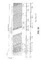
- FIGS. 8A , 8 B, 8 C and 8 D are charts illustrating conditions enabling expressions by all gradations
- FIG. 9 is a block diagram showing the configuration of a conventional pixel circuit 1 ;
- FIG. 10 is a timing chart of the conventional pixel circuit 1 ;
- FIG. 11 is a block diagram showing a make-up of another conventional pixel circuit 1 ;
- FIG. 12 is a timing chart of the another conventional pixel circuit 2 ;
- FIG. 13 is a timing chart showing a state of light emitting in 6 bit gradations of the another conventional pixel circuit 2 ;
- FIG. 14 is a block diagram showing an example configuration of another pixel circuit
- FIG. 15A is a block diagram explaining operations of the pixel circuit shown in FIG. 14 ;
- FIG. 15B is a block diagram explaining operations of the pixel circuit shown in FIG. 14 ;
- FIG. 15C is a block diagram explaining operations of the pixel circuit shown in FIG. 14 ;
- FIG. 16 is a table explaining operations of the pixel circuit shown in FIG. 14 .
- FIG. 1 shows a display device in which the present invention is applied
- FIG. 2A shows a timing chart for explaining an operation thereof.
- a source supply circuit 4 is connected with a positive source line 12 maintained at a voltage V DD and a negative source line 13 maintained at a voltage V SS , which extend to respective pixels.
- signal lines 14 for supplying signal voltages corresponding to luminance signals of respective pixels extend along respective columns.
- a first and second scanning lines 10 , 11 for controlling seizure of signal voltages at respective pixels extend along respective rows.
- Each of the pixels is provided with an n-channel switching element 15 , a capacitance 16 , a p-channel driver element 17 , and a light emitting element 18 .
- the switching element 15 has the drain or the source being connected with the signal line 14 , the source or the drain being connected with the gate of the driver element 17 , and the gate being connected with the first scanning line 10 . It should be noted that a p-channel switching element 15 may be used.
- One end of the capacitance 16 is connected with the gate of the driver element 17 , and the other end of the capacitance 16 is connected with the second scanning line 11 .
- the source of the driver element 17 is connected with the positive source line 12 , and the drain thereof is connected with an anode electrode of the light emitting element 18 .
- a cathode electrode of the light emitting element 18 is connected with the negative source line 13 .
- one frame is made up of a plurality of subframes, and one subframe thereof is divided into a data writing period and two sub-subframes, the sub-subframes being determined by a level of the second scanning line 11 .
- the subframes correspond to either State A or State B in FIG. 5 , depending on the level of the second scanning line 11 .
- the signal voltage of the signal line 14 is set at any one of V 0 , V 0 ⁇ V D1 , or V 0 ⁇ V D1 ⁇ V D2 by the signal line driving circuit 2 and, after the second scanning line 11 is set to a low voltage V L by a scanning line driving circuit 3 , the first scanning line 10 is controlled by the scanning line driving circuit 3 such that the switching element 15 is in conductive state ( FIG. 3A ). Thereafter, a pixel enters into a sub-subframe which is either in the State A or State B depending on the state of the second scanning line 11 . In other words, when the second scanning line 11 is set at V L , the sub-subframe is in the State A, and when it is set at V H , the sub-subframe is in the State B ( FIG. 5 ).
- V H , V L , V 0 , V D1 , and V D2 are set such that the following below-noted relationships are satisfied when a threshold voltage of the driver element 17 is set at V t .
- V t is set equal to 0.
- V t Formula 1
- the time ratio between the sub-subframes of the State A and State B in one subframe is controlled by the timing of the second scanning line 11 . Accordingly, the time ratio of the sub-subframes can be controlled by controlling the duty ratio of the second scanning line 11 . It is also possible that the sequence of the State A and State B can be altered in an arbitrary subframe as shown in FIG. 2B .
- the false contour can be reduced by approximation to the light emitting characteristic shown in FIG. 13 as described in the non-patent art discussed above, without increasing the refreshing number as n+m times as described in the cited patent application. Furthermore, because a duty ratio of almost 100% can be secured by the method according to the present embodiment in conjunction with the related art method described above, which does not generate false contours, the current density of the light emitting element at the time of light emitting can be reduced enabling elongation of lifetime and reduction of power consumption of the light emitting element; both are clearly advantages.
- FIGS. 4A to 4C show the configuration and operation of another embodiment of the present invention.
- the gate of the driver element 17 is connected with one end of capacitance 19 , other end thereof being maintained at a constant voltage supplied from a source supply circuit 4 .
- the capacitance 19 is also charged.
- FIG. 4B even when the switching element 15 is turned off, the gate voltage of the driver element 17 is maintained at V data .
- the gate voltage of the driver element 17 is changed to the one expressed by a mathematical formula V data +[C 1 /(C 2 +C 2 )](V gH ⁇ V gL ).
- C 1 is a capacity value of the capacitance 16
- C 2 is the capacity value of the capacitance 19 .
- the source voltage to which the other end of the capacitance 19 is connected may be any voltage as long as it is constant, a preferable voltage is that held by the source supply circuit 4 , namely, V SS or the like.
- FIG. 7A shows an example of control in case of 4 bits (16 gradations).
- four subframes 1 to 4 are prepared. Then, the subframe 1 having a total length of 4 units is divided into two sub-subframes, the first half thereof having a length of 3 units and the second half having a length of 1 unit (3:1), with the second half being the priority light emitting period; the subframe 2 having a total length of 4 units is divided into two sub-subframes, each of the first half and the second half thereof having a length of 2 units, respectively (2:2), with the second half being the priority light emitting period; the subframe 3 having a total length of 4 units is divided into two sub-subframes, each of the first half and the second half thereof having a length of 2 units, respectively (2:2), with the first half being the priority light emitting period; and the subframe 4 having a total length of 3 units is divided into two sub-subframes, the first half thereof having a length of 2 units and the second half having a length of 1 unit
- the subframe 1 having a total length of 7 units is divided into two sub-subframes, the first half thereof having a length of 6 units and the second half having a length of 1 unit (6:1), with the second half being the priority light emitting period;
- the subframe 2 having a total length of 6 units is divided into two sub-subframes, the first half thereof having a length of 4 units and the second half having a length of 2 units (4:2), with the second half being the priority light emitting period;
- the subframe 3 having a total length of 6 units is divided into two sub-subframes, each of the first half and the second half thereof having a length of 3 units, respectively (3:3), with the first half being the priority light emitting period;
- the subframe 4 having a total length of 6 units is divided into two sub-subframes, the first half thereof having a length of 4 units and the second half having a length of 2 units (4:2), with the first half
- the duty ratio of 0 to 100% can be realized by preparing 6 subframes and providing sub-subframes of 10:1, 9:2, 7:4, 6:4, 8:2, and 9:1. It should be noted that other examples of make-up of sub-subframes which realize display of 6 bits (64 gradations) with 6 subframes are also available, such as shown in FIG. 7D .
- the number of subframes corresponding to the number of gradations necessary for display is determined in the following manner in accordance with the number of gradations of the sub-subframes.
- the number of the gradations of a display device is set as n bits, and the number of the subframes is set as m.
- the number of gradations desirably expressed is expressed, in this manner, utilizing the sub-subframes.
- the frequency of the subframe does not change even if the duty ratio between two sub-subframes within one subframe is altered. Accordingly, display of larger gradations can be achieved while maintaining a small subframe display rate.
- FIG. 14 shows another example of pixel circuit makeup.
- an anode of the light emitting element 18 is connected with the positive source line 12
- a cathode thereof is connected with the drain of the n-channel driver element 17
- the source of the driver element 17 is connected with the negative source line 13 .
- a switching element 21 for short-circuiting is provided between the drain and the gate of the driver element 17 , and the gate of the switching element 21 for short-circuiting is connected with the first scanning line 10 .
- a capacitance 16 is arranged between the gate of the driver element 17 and the source or drain of the switching element 15 (on a side which is not connected with the signal line 14 ).
- the switching element 15 and the switching element 21 for short-circuiting are turned on by setting the first scanning line 10 at H level as shown in FIGS. 15A to 15C , a voltage higher by the threshold voltage V t than the voltage V SS of the negative source line 13 is written in the gate of the driver element 17 , and a signal voltage is written in the connection of the switching element 15 with the capacitance 16 . Then, after setting the first scanning line 10 at L level, the voltage of the second scanning line is set at a predetermined voltage and the third scanning line 22 is set at H level, then the gate voltage of the driver element 17 can be controlled in the same way as above described as shown in FIG. 16 . In this way, V t compensation is provided by this pixel circuit.
Abstract
Description
V DD −V 0 <−V t
V DD−(V 0 −V D1)>−V t
V DD−(V 0 −V D1)−(V H −V L)<−V t
V DD−(V 0 −V D1 −V D2)−(V H −V L)>−V t Formula 1
[2n/m] or [2n/m]−1 (here [ ] is gauss notation) and
(1(≦2p) or 2n−1, P=0, 1, 2, . . . , P≦m/2).
It is preferable that the number of subframes m is the minimum value of k which satisfies the above formula.
2k≧2n/(2k+1)−2k
Preferably, the number of subframes of m expressed by k is the minimum number for satisfying the above formula.
It is preferable that the number of subframes m is the minimum value of k which satisfies the above formula.
2k≧2n/2k−2k
It is preferable that the number of subframes m is the minimum value of k which satisfies the above formula.
- 3 driving circuit
- 4 supply circuit
- 10 scanning line
- 11 scanning line
- 12 source line
- 13 source line
- 14 signal lines
- 15 switching element
- 16 capacitance
- 17 driver element
- 18 light emitting element
- 19 capacitance
- 21 switching element
- 22 scanning line
- 101 scanning line
- 102 scanning line
- 103 signal line
- 104 driver element
- 105 light emitting element
- 106 driving circuit
- 107 supply circuit
- 108 driving circuit
- 109 switching element
- 110 discharge switch
- 111 capacitance
- 201 scanning line
- 202 scanning line
- 203 signal line
- 204 driver element
- 205 light emitting element
- 206 driving circuit
- 207 supply circuit
- 208 driving circuit
- 209 switching element
- 210 switching element
- 211 capacitance
Claims (8)
Applications Claiming Priority (3)
| Application Number | Priority Date | Filing Date | Title |
|---|---|---|---|
| JP2005-250303 | 2005-08-30 | ||
| JP2005250303A JP4773777B2 (en) | 2005-08-30 | 2005-08-30 | Active matrix display device |
| PCT/US2006/033314 WO2007027534A1 (en) | 2005-08-30 | 2006-08-24 | Active matrix-type display device |
Publications (2)
| Publication Number | Publication Date |
|---|---|
| US20090015522A1 US20090015522A1 (en) | 2009-01-15 |
| US8013813B2 true US8013813B2 (en) | 2011-09-06 |
Family
ID=37311865
Family Applications (1)
| Application Number | Title | Priority Date | Filing Date |
|---|---|---|---|
| US12/064,091 Active 2028-09-05 US8013813B2 (en) | 2005-08-30 | 2006-08-24 | Active matrix-type display device |
Country Status (4)
| Country | Link |
|---|---|
| US (1) | US8013813B2 (en) |
| EP (1) | EP1920430B1 (en) |
| JP (1) | JP4773777B2 (en) |
| WO (1) | WO2007027534A1 (en) |
Cited By (1)
| Publication number | Priority date | Publication date | Assignee | Title |
|---|---|---|---|---|
| US20140292826A1 (en) * | 2013-04-02 | 2014-10-02 | Samsung Display Co., Ltd. | Display panel driver, method of driving display panel using the same, and display apparatus having the same |
Families Citing this family (7)
| Publication number | Priority date | Publication date | Assignee | Title |
|---|---|---|---|---|
| JP2010091879A (en) * | 2008-10-09 | 2010-04-22 | Nippon Hoso Kyokai <Nhk> | Display driving circuit and display device using the same |
| SG10201913006XA (en) * | 2009-10-30 | 2020-02-27 | Univ North Carolina Chapel Hill | Multipotent stem cells from the extrahepatic billary tree and methods of isolating same |
| KR101560239B1 (en) * | 2010-11-18 | 2015-10-26 | 엘지디스플레이 주식회사 | Organic light emitting diode display device and method for driving the same |
| KR101969959B1 (en) * | 2012-05-25 | 2019-04-18 | 삼성디스플레이 주식회사 | Method of digital-driving an organic light emitting display device |
| US11127357B2 (en) * | 2019-04-19 | 2021-09-21 | Apple Inc. | Display pixel luminance stabilization systems and methods |
| CN110782835A (en) * | 2019-11-29 | 2020-02-11 | 深圳市华星光电半导体显示技术有限公司 | Method for improving OVSS voltage drop of OLED display panel and OLED display panel |
| WO2023139792A1 (en) * | 2022-01-24 | 2023-07-27 | シャープディスプレイテクノロジー株式会社 | Display device |
Citations (17)
| Publication number | Priority date | Publication date | Assignee | Title |
|---|---|---|---|---|
| JPH10214060A (en) | 1997-01-28 | 1998-08-11 | Casio Comput Co Ltd | Electric field light emission display device and its driving method |
| EP0895219A1 (en) | 1997-02-17 | 1999-02-03 | Seiko Epson Corporation | Display device |
| JPH11338402A (en) | 1998-04-30 | 1999-12-10 | Hewlett Packard Co <Hp> | Display device |
| US20020047852A1 (en) | 2000-09-04 | 2002-04-25 | Kazutaka Inukai | Method of driving EL display device |
| JP2003223136A (en) | 2002-01-31 | 2003-08-08 | Hitachi Ltd | Display device and its driving method |
| JP2003223137A (en) | 2002-01-31 | 2003-08-08 | Hitachi Ltd | Display device and its driving method |
| US20040066359A1 (en) * | 2002-10-03 | 2004-04-08 | Pioneer Corporation | Light-emission drive circuit for organic electroluminescence element and display device |
| US20040239599A1 (en) * | 2000-10-24 | 2004-12-02 | Semiconductor Energy Laboratory Co., Ltd., A Japan Corporation | Light emitting device and method of driving the same |
| JP2005031643A (en) | 2003-06-20 | 2005-02-03 | Sanyo Electric Co Ltd | Light emitting device and display device |
| US20050110723A1 (en) * | 2003-11-25 | 2005-05-26 | Dong-Yong Shin | Pixel circuit in flat panel display device and method for driving the same |
| US20050212408A1 (en) * | 2004-03-29 | 2005-09-29 | Tohoku Pioneer Corporation | Drive unit for light-emitting display panel, and electronic device mounted therewith |
| WO2006012028A1 (en) | 2004-06-30 | 2006-02-02 | Eastman Kodak Company | Active matrix display device |
| US20060044229A1 (en) * | 2004-08-27 | 2006-03-02 | Semiconductor Energy Laboratory Co., Ltd. | Display device and driving method thereof |
| US20060077138A1 (en) * | 2004-09-15 | 2006-04-13 | Kim Hong K | Organic light emitting display and driving method thereof |
| US20060119554A1 (en) * | 2004-12-06 | 2006-06-08 | Semiconductor Energy Laboratory Co., Ltd. | Display device, driving method thereof and electronic appliance |
| US20060220572A1 (en) * | 2005-03-29 | 2006-10-05 | Tohoku Pioneer Corporation | Driving device of luminescent display panel and driving method of the same |
| US20070103405A1 (en) * | 2005-11-04 | 2007-05-10 | Kwak Won Kyu | Organic light emitting display device and driving method thereof |
-
2005
- 2005-08-30 JP JP2005250303A patent/JP4773777B2/en active Active
-
2006
- 2006-08-24 EP EP06790008.4A patent/EP1920430B1/en active Active
- 2006-08-24 US US12/064,091 patent/US8013813B2/en active Active
- 2006-08-24 WO PCT/US2006/033314 patent/WO2007027534A1/en active Application Filing
Patent Citations (17)
| Publication number | Priority date | Publication date | Assignee | Title |
|---|---|---|---|---|
| JPH10214060A (en) | 1997-01-28 | 1998-08-11 | Casio Comput Co Ltd | Electric field light emission display device and its driving method |
| EP0895219A1 (en) | 1997-02-17 | 1999-02-03 | Seiko Epson Corporation | Display device |
| JPH11338402A (en) | 1998-04-30 | 1999-12-10 | Hewlett Packard Co <Hp> | Display device |
| US20020047852A1 (en) | 2000-09-04 | 2002-04-25 | Kazutaka Inukai | Method of driving EL display device |
| US20040239599A1 (en) * | 2000-10-24 | 2004-12-02 | Semiconductor Energy Laboratory Co., Ltd., A Japan Corporation | Light emitting device and method of driving the same |
| JP2003223136A (en) | 2002-01-31 | 2003-08-08 | Hitachi Ltd | Display device and its driving method |
| JP2003223137A (en) | 2002-01-31 | 2003-08-08 | Hitachi Ltd | Display device and its driving method |
| US20040066359A1 (en) * | 2002-10-03 | 2004-04-08 | Pioneer Corporation | Light-emission drive circuit for organic electroluminescence element and display device |
| JP2005031643A (en) | 2003-06-20 | 2005-02-03 | Sanyo Electric Co Ltd | Light emitting device and display device |
| US20050110723A1 (en) * | 2003-11-25 | 2005-05-26 | Dong-Yong Shin | Pixel circuit in flat panel display device and method for driving the same |
| US20050212408A1 (en) * | 2004-03-29 | 2005-09-29 | Tohoku Pioneer Corporation | Drive unit for light-emitting display panel, and electronic device mounted therewith |
| WO2006012028A1 (en) | 2004-06-30 | 2006-02-02 | Eastman Kodak Company | Active matrix display device |
| US20060044229A1 (en) * | 2004-08-27 | 2006-03-02 | Semiconductor Energy Laboratory Co., Ltd. | Display device and driving method thereof |
| US20060077138A1 (en) * | 2004-09-15 | 2006-04-13 | Kim Hong K | Organic light emitting display and driving method thereof |
| US20060119554A1 (en) * | 2004-12-06 | 2006-06-08 | Semiconductor Energy Laboratory Co., Ltd. | Display device, driving method thereof and electronic appliance |
| US20060220572A1 (en) * | 2005-03-29 | 2006-10-05 | Tohoku Pioneer Corporation | Driving device of luminescent display panel and driving method of the same |
| US20070103405A1 (en) * | 2005-11-04 | 2007-05-10 | Kwak Won Kyu | Organic light emitting display device and driving method thereof |
Non-Patent Citations (1)
| Title |
|---|
| H. Kageyama et al, 51:1: A 2.5 inch OLED Display with a Three-TFT Pixel Circuit for Clamped Inverter Driving, SID 04 Digest, pp. 1394-1397, 2004. |
Cited By (2)
| Publication number | Priority date | Publication date | Assignee | Title |
|---|---|---|---|---|
| US20140292826A1 (en) * | 2013-04-02 | 2014-10-02 | Samsung Display Co., Ltd. | Display panel driver, method of driving display panel using the same, and display apparatus having the same |
| US9443467B2 (en) * | 2013-04-02 | 2016-09-13 | Samsung Display Co., Ltd. | Display panel driver, method of driving display panel using the same, and display apparatus having the same |
Also Published As
| Publication number | Publication date |
|---|---|
| US20090015522A1 (en) | 2009-01-15 |
| EP1920430A1 (en) | 2008-05-14 |
| JP4773777B2 (en) | 2011-09-14 |
| WO2007027534A1 (en) | 2007-03-08 |
| JP2007065218A (en) | 2007-03-15 |
| EP1920430B1 (en) | 2015-11-04 |
Similar Documents
| Publication | Publication Date | Title |
|---|---|---|
| KR101143009B1 (en) | Display device and driving method thereof | |
| US7545354B2 (en) | Driving circuit active matrix type organic light emitting diode device and method thereof | |
| KR100515305B1 (en) | Light emitting display device and display panel and driving method thereof | |
| JP4024557B2 (en) | Light emitting device, electronic equipment | |
| US7561128B2 (en) | Organic electroluminescence display device | |
| US8013813B2 (en) | Active matrix-type display device | |
| US7164401B2 (en) | Light emitting display, display panel, and driving method thereof | |
| US7928945B2 (en) | Display device and driving method thereof | |
| US6870553B2 (en) | Drive circuit to be used in active matrix type light-emitting element array | |
| US7652645B2 (en) | Light emitting display | |
| KR101112555B1 (en) | Display device and driving method thereof | |
| US20050151135A1 (en) | Light-emitting device, and electric device using the same | |
| US20050007319A1 (en) | Display panel, light emitting display using the display panel, and driving method thereof | |
| JP4244617B2 (en) | Electro-optical device and driving method of electro-optical device | |
| JP2004334163A (en) | Image display panel, image display device, method for driving image display device, and pixel circuit | |
| KR100529077B1 (en) | Image display apparatus, display panel and driving method thereof | |
| JP2004170815A (en) | El display device and method for driving the same | |
| KR20070111634A (en) | Pixel circuit of organic light emitting display | |
| JP2004038176A (en) | Electroluminescence panel and electroluminescence device with same | |
| US7463224B2 (en) | Light emitting device and display device | |
| JP2005134880A (en) | Image display apparatus, driving method thereof, and precharge voltage setting method | |
| JPWO2002077958A1 (en) | Driver circuit for active matrix light emitting device | |
| JP3923341B2 (en) | Semiconductor integrated circuit and driving method thereof | |
| US9064454B2 (en) | Display device and method of driving the same | |
| JP2002287682A (en) | Display panel and method for driving the same |
Legal Events
| Date | Code | Title | Description |
|---|---|---|---|
| AS | Assignment |
Owner name: EASTMAN KODAK COMPANY, NEW YORK Free format text: ASSIGNMENT OF ASSIGNORS INTEREST;ASSIGNOR:ONO, SHINYO;REEL/FRAME:020523/0374 Effective date: 20071118 |
|
| AS | Assignment |
Owner name: GLOBAL OLED TECHNOLOGY LLC,DELAWARE Free format text: ASSIGNMENT OF ASSIGNORS INTEREST;ASSIGNOR:EASTMAN KODAK COMPANY;REEL/FRAME:024068/0468 Effective date: 20100304 Owner name: GLOBAL OLED TECHNOLOGY LLC, DELAWARE Free format text: ASSIGNMENT OF ASSIGNORS INTEREST;ASSIGNOR:EASTMAN KODAK COMPANY;REEL/FRAME:024068/0468 Effective date: 20100304 |
|
| STCF | Information on status: patent grant |
Free format text: PATENTED CASE |
|
| FPAY | Fee payment |
Year of fee payment: 4 |
|
| MAFP | Maintenance fee payment |
Free format text: PAYMENT OF MAINTENANCE FEE, 8TH YEAR, LARGE ENTITY (ORIGINAL EVENT CODE: M1552); ENTITY STATUS OF PATENT OWNER: LARGE ENTITY Year of fee payment: 8 |
|
| MAFP | Maintenance fee payment |
Free format text: PAYMENT OF MAINTENANCE FEE, 12TH YEAR, LARGE ENTITY (ORIGINAL EVENT CODE: M1553); ENTITY STATUS OF PATENT OWNER: LARGE ENTITY Year of fee payment: 12 |