US8022382B2 - Phase change memory devices with reduced programming current - Google Patents
Phase change memory devices with reduced programming current Download PDFInfo
- Publication number
- US8022382B2 US8022382B2 US11/368,192 US36819206A US8022382B2 US 8022382 B2 US8022382 B2 US 8022382B2 US 36819206 A US36819206 A US 36819206A US 8022382 B2 US8022382 B2 US 8022382B2
- Authority
- US
- United States
- Prior art keywords
- phase change
- layer
- memory device
- electrode
- change memory
- Prior art date
- Legal status (The legal status is an assumption and is not a legal conclusion. Google has not performed a legal analysis and makes no representation as to the accuracy of the status listed.)
- Expired - Fee Related, expires
Links
- 230000008859 change Effects 0.000 title claims abstract description 93
- 239000000463 material Substances 0.000 claims description 19
- 229910010037 TiAlN Inorganic materials 0.000 claims description 9
- OKTJSMMVPCPJKN-UHFFFAOYSA-N Carbon Chemical compound [C] OKTJSMMVPCPJKN-UHFFFAOYSA-N 0.000 claims description 6
- 229910052799 carbon Inorganic materials 0.000 claims description 6
- 239000002178 crystalline material Substances 0.000 claims description 5
- 229910052718 tin Inorganic materials 0.000 claims description 5
- 229910010038 TiAl Inorganic materials 0.000 claims description 3
- 229910052738 indium Inorganic materials 0.000 claims description 2
- 150000002736 metal compounds Chemical group 0.000 claims description 2
- 229910052709 silver Inorganic materials 0.000 claims description 2
- 229910052787 antimony Inorganic materials 0.000 claims 1
- 229910052733 gallium Inorganic materials 0.000 claims 1
- 239000012782 phase change material Substances 0.000 abstract description 28
- 238000000034 method Methods 0.000 abstract description 26
- 239000010410 layer Substances 0.000 description 118
- 230000008569 process Effects 0.000 description 17
- 238000010438 heat treatment Methods 0.000 description 9
- 238000004519 manufacturing process Methods 0.000 description 6
- 150000004770 chalcogenides Chemical class 0.000 description 5
- 238000002425 crystallisation Methods 0.000 description 5
- 230000008025 crystallization Effects 0.000 description 5
- 238000009413 insulation Methods 0.000 description 5
- 229910052751 metal Inorganic materials 0.000 description 5
- 239000002184 metal Substances 0.000 description 5
- CSCPPACGZOOCGX-UHFFFAOYSA-N Acetone Chemical compound CC(C)=O CSCPPACGZOOCGX-UHFFFAOYSA-N 0.000 description 4
- 238000005275 alloying Methods 0.000 description 4
- 239000002131 composite material Substances 0.000 description 4
- 230000020169 heat generation Effects 0.000 description 4
- 239000012212 insulator Substances 0.000 description 4
- 229920002120 photoresistant polymer Polymers 0.000 description 4
- 230000000171 quenching effect Effects 0.000 description 4
- 239000004065 semiconductor Substances 0.000 description 4
- 239000000758 substrate Substances 0.000 description 4
- ATJFFYVFTNAWJD-UHFFFAOYSA-N Tin Chemical compound [Sn] ATJFFYVFTNAWJD-UHFFFAOYSA-N 0.000 description 3
- 230000008901 benefit Effects 0.000 description 3
- 239000004020 conductor Substances 0.000 description 3
- 239000003989 dielectric material Substances 0.000 description 3
- 230000006870 function Effects 0.000 description 3
- 230000008018 melting Effects 0.000 description 3
- 238000002844 melting Methods 0.000 description 3
- 239000000203 mixture Substances 0.000 description 3
- 238000010791 quenching Methods 0.000 description 3
- IJGRMHOSHXDMSA-UHFFFAOYSA-N Atomic nitrogen Chemical compound N#N IJGRMHOSHXDMSA-UHFFFAOYSA-N 0.000 description 2
- 229910052581 Si3N4 Inorganic materials 0.000 description 2
- VYPSYNLAJGMNEJ-UHFFFAOYSA-N Silicium dioxide Chemical compound O=[Si]=O VYPSYNLAJGMNEJ-UHFFFAOYSA-N 0.000 description 2
- XUIMIQQOPSSXEZ-UHFFFAOYSA-N Silicon Chemical compound [Si] XUIMIQQOPSSXEZ-UHFFFAOYSA-N 0.000 description 2
- 229910052782 aluminium Inorganic materials 0.000 description 2
- 230000015572 biosynthetic process Effects 0.000 description 2
- 229910052802 copper Inorganic materials 0.000 description 2
- 239000010949 copper Substances 0.000 description 2
- 230000003247 decreasing effect Effects 0.000 description 2
- 238000000151 deposition Methods 0.000 description 2
- 230000000694 effects Effects 0.000 description 2
- 150000004767 nitrides Chemical class 0.000 description 2
- 238000005240 physical vapour deposition Methods 0.000 description 2
- 229910052710 silicon Inorganic materials 0.000 description 2
- 239000010703 silicon Substances 0.000 description 2
- HQVNEWCFYHHQES-UHFFFAOYSA-N silicon nitride Chemical compound N12[Si]34N5[Si]62N3[Si]51N64 HQVNEWCFYHHQES-UHFFFAOYSA-N 0.000 description 2
- 229910052814 silicon oxide Inorganic materials 0.000 description 2
- 125000006850 spacer group Chemical group 0.000 description 2
- 229910052721 tungsten Inorganic materials 0.000 description 2
- 229910016570 AlCu Inorganic materials 0.000 description 1
- 229910017150 AlTi Inorganic materials 0.000 description 1
- RYGMFSIKBFXOCR-UHFFFAOYSA-N Copper Chemical compound [Cu] RYGMFSIKBFXOCR-UHFFFAOYSA-N 0.000 description 1
- 229910000881 Cu alloy Inorganic materials 0.000 description 1
- ZOKXTWBITQBERF-UHFFFAOYSA-N Molybdenum Chemical compound [Mo] ZOKXTWBITQBERF-UHFFFAOYSA-N 0.000 description 1
- 239000004642 Polyimide Substances 0.000 description 1
- 230000004075 alteration Effects 0.000 description 1
- XAGFODPZIPBFFR-UHFFFAOYSA-N aluminium Chemical compound [Al] XAGFODPZIPBFFR-UHFFFAOYSA-N 0.000 description 1
- XKRFYHLGVUSROY-UHFFFAOYSA-N argon Substances [Ar] XKRFYHLGVUSROY-UHFFFAOYSA-N 0.000 description 1
- 229910052786 argon Inorganic materials 0.000 description 1
- 230000008021 deposition Effects 0.000 description 1
- 238000005516 engineering process Methods 0.000 description 1
- 230000017525 heat dissipation Effects 0.000 description 1
- 239000012774 insulation material Substances 0.000 description 1
- 239000011229 interlayer Substances 0.000 description 1
- 229910052750 molybdenum Inorganic materials 0.000 description 1
- 239000011733 molybdenum Substances 0.000 description 1
- 229910052757 nitrogen Inorganic materials 0.000 description 1
- 238000000206 photolithography Methods 0.000 description 1
- 229920001721 polyimide Polymers 0.000 description 1
- 238000004544 sputter deposition Methods 0.000 description 1
- 238000006467 substitution reaction Methods 0.000 description 1
- WFKWXMTUELFFGS-UHFFFAOYSA-N tungsten Chemical compound [W] WFKWXMTUELFFGS-UHFFFAOYSA-N 0.000 description 1
- 239000010937 tungsten Substances 0.000 description 1
- 238000001039 wet etching Methods 0.000 description 1
Images


Classifications
-
- H—ELECTRICITY
- H10—SEMICONDUCTOR DEVICES; ELECTRIC SOLID-STATE DEVICES NOT OTHERWISE PROVIDED FOR
- H10N—ELECTRIC SOLID-STATE DEVICES NOT OTHERWISE PROVIDED FOR
- H10N70/00—Solid-state devices without a potential-jump barrier or surface barrier, and specially adapted for rectifying, amplifying, oscillating or switching
- H10N70/20—Multistable switching devices, e.g. memristors
- H10N70/231—Multistable switching devices, e.g. memristors based on solid-state phase change, e.g. between amorphous and crystalline phases, Ovshinsky effect
-
- H—ELECTRICITY
- H10—SEMICONDUCTOR DEVICES; ELECTRIC SOLID-STATE DEVICES NOT OTHERWISE PROVIDED FOR
- H10N—ELECTRIC SOLID-STATE DEVICES NOT OTHERWISE PROVIDED FOR
- H10N70/00—Solid-state devices without a potential-jump barrier or surface barrier, and specially adapted for rectifying, amplifying, oscillating or switching
- H10N70/011—Manufacture or treatment of multistable switching devices
- H10N70/061—Patterning of the switching material
-
- H—ELECTRICITY
- H10—SEMICONDUCTOR DEVICES; ELECTRIC SOLID-STATE DEVICES NOT OTHERWISE PROVIDED FOR
- H10N—ELECTRIC SOLID-STATE DEVICES NOT OTHERWISE PROVIDED FOR
- H10N70/00—Solid-state devices without a potential-jump barrier or surface barrier, and specially adapted for rectifying, amplifying, oscillating or switching
- H10N70/801—Constructional details of multistable switching devices
- H10N70/821—Device geometry
- H10N70/826—Device geometry adapted for essentially vertical current flow, e.g. sandwich or pillar type devices
-
- H—ELECTRICITY
- H10—SEMICONDUCTOR DEVICES; ELECTRIC SOLID-STATE DEVICES NOT OTHERWISE PROVIDED FOR
- H10N—ELECTRIC SOLID-STATE DEVICES NOT OTHERWISE PROVIDED FOR
- H10N70/00—Solid-state devices without a potential-jump barrier or surface barrier, and specially adapted for rectifying, amplifying, oscillating or switching
- H10N70/801—Constructional details of multistable switching devices
- H10N70/841—Electrodes
- H10N70/8413—Electrodes adapted for resistive heating
-
- H—ELECTRICITY
- H10—SEMICONDUCTOR DEVICES; ELECTRIC SOLID-STATE DEVICES NOT OTHERWISE PROVIDED FOR
- H10N—ELECTRIC SOLID-STATE DEVICES NOT OTHERWISE PROVIDED FOR
- H10N70/00—Solid-state devices without a potential-jump barrier or surface barrier, and specially adapted for rectifying, amplifying, oscillating or switching
- H10N70/801—Constructional details of multistable switching devices
- H10N70/861—Thermal details
-
- H—ELECTRICITY
- H10—SEMICONDUCTOR DEVICES; ELECTRIC SOLID-STATE DEVICES NOT OTHERWISE PROVIDED FOR
- H10N—ELECTRIC SOLID-STATE DEVICES NOT OTHERWISE PROVIDED FOR
- H10N70/00—Solid-state devices without a potential-jump barrier or surface barrier, and specially adapted for rectifying, amplifying, oscillating or switching
- H10N70/801—Constructional details of multistable switching devices
- H10N70/881—Switching materials
- H10N70/882—Compounds of sulfur, selenium or tellurium, e.g. chalcogenides
- H10N70/8828—Tellurides, e.g. GeSbTe
Definitions
- This invention relates generally to phase change memory devices, and more particularly to the structures and manufacturing methods of phase change memory devices having reduced programming current.
- Phase change technology is promising for next generation memory devices. It uses chalcogenide semiconductors for storing states and digital information.
- the chalcogenide semiconductors also called phase change materials, have a crystalline state and an amorphous state. In the crystalline state, the phase change materials have low resistivity; while in the amorphous state, they have high resistivity.
- the resistivity ratios of the phase change material in the amorphous and crystalline states are typically greater than 1000, and thus the phase change memory devices are unlikely to have errors for reading states.
- the chalcogenide semiconductors are stable at a certain temperature range in both crystalline and amorphous states and can be switched back and forth between the two states by electric pulses. Because of the large resistivity ratio of the crystalline and amorphous states of the phase change material, the resistivities of intermediate states between crystalline and amorphous can also show good enough resolution for multilevel recording.
- the multilevel recording is another advantage of phase change memory.
- a phase change memory device is formed by placing a phase change material between two electrodes.
- Write operations also called programming operations, which apply electric pulses to the memory device
- read operations which measure the resistance of the phase change memory
- FIG. 1 illustrates required temperatures for typical programming operations. The temperatures are illustrated as a function of time.
- a set operation that crystallizes the phase change material is illustrated as line 4 .
- the set pulse needs to heat up the phase change material to a temperature higher than a crystallization temperature T x , but below a melting temperature T m , for a time t 2 longer than the required crystalline time, for the crystallization to take place.
- a reset operation that turns the phase change material into an amorphous state is illustrated by line 2 .
- the reset pulse needs to heat up the phase change material to a temperature higher than the melting temperature T m .
- the temperature is then quickly dropped below the crystallization temperature T x during a time period t 1 , which must be short enough to avoid the crystallization from occurring.
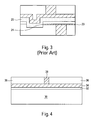
- FIG. 2 illustrates a conventional phase change memory device having reduced contact area.
- a trench 10 is formed in an insulator 12 .
- a conductive interfacial layer 14 is formed covering the trench 10 and insulator 12 .
- Spacers 16 are formed in trench 10 .
- Phase change material is then deposited into the remainder of the trench to form a phase change layer 18 . Since the contact area 17 between the phase change material layer 18 and the interfacial layer is reduced by the spacers 16 , the effective resistance is increased and the required programming current is reduced.
- the reset speed is mainly on the intrinsic property of the phase change materials.
- FIG. 3 illustrates a prior art phase change memory device having an edge contact.
- Phase change material layer 26 has a contact region 24 with the edge of a conductive line 20 . Since it is easy to form a thin conductive line 20 , the contact region 24 can have an area as small 0.004 ⁇ m 2 . Therefore, the required current density is significantly reduced.
- the prior art solutions suffer some drawbacks, however.
- the memory device of the prior art may have an undesirable high current density at an interface area, causing alloying of a phase change material and its neighboring material. It is harder to control programming current density in a manageable range when the contact area is very small, hence the control is inaccurate. Inaccurately controlled current density may cause instability of state change in the reset operation. Therefore, there is a need for alternative solutions.
- a phase change memory device includes a conducting electrode in a dielectric layer, a bottom electrode over the conducting electrode, a phase change layer over the bottom electrode, and a top electrode over the phase change layer. Resistivities of the bottom electrode and the top electrode are greater than a resistivity of the phase change layer in a crystalline state.
- a phase change memory device includes a conducting electrode in a dielectric layer, wherein the conducting electrode has a top surface, an insulation layer over the dielectric layer, an opening in the insulation layer wherein the opening is above the conducting electrode and has an area greater than an area of the top surface of the conducting electrode, and stacked layers filled in the opening.
- the stacked layers include a bottom electrode over the conducting electrode and the dielectric layer, a phase change layer over the bottom electrode, a heat sink layer over the bottom electrode, and a top electrode over the phase change layer.
- the conducting electrode has a top interface having a first area
- the bottom electrode has a top interface having a second area in contact with the phase change layer.
- the second area and the first area preferably have a ratio of greater than one.
- the preferred embodiment has several advantageous features.
- higher resistivity of the bottom electrode and top electrode help the concentration of the current and reduce the required programming current. Also, fewer errors occur due to reduced current density.
- a higher ratio of the area of the bottom electrode to the top surface area of the conducting electrode reduces alloying of the bottom electrode with the phase change material.
- the combination of lift-off technique and stacked layer design in some embodiments reduces the number of masks required for forming the phase change memory device.
- FIG. 1 illustrates required temperatures for programming phase change devices as a function of time
- FIG. 2 illustrates a conventional phase change memory device having a reduced contact area
- FIG. 3 illustrates a conventional phase change memory device having an edge contact
- FIGS. 4 through 7 b are cross-sectional views of intermediate stages in the manufacture of preferred phase change memory device embodiments.
- FIGS. 8 and 9 show I-V curves of samples having the preferred structure.
- FIGS. 4 through 7 The intermediate stages of manufacturing a novel phase change memory device embodiment of the present invention are illustrated in FIGS. 4 through 7 .
- like reference numbers are used to designate like elements.
- FIG. 4 illustrates a composite structure.
- An insulation layer 32 is formed over a substrate 30 and electrically insulates the memory structures that will be subsequently formed.
- Substrate 30 may be a silicon substrate or a substrate comprising other semiconductor materials.
- the insulation layer 32 may comprise oxide such as silicon oxide, silicon nitride, or other dielectric materials.
- a bottom metal line 34 is formed on the insulation layer 32 .
- the bottom metal line 34 is formed of copper or copper alloys, preferably by a damascene process.
- the bottom metal line 34 can be formed of conductive materials such as aluminum, tungsten, etc.
- a conducting electrode 38 is then formed.
- the conducting electrode 38 is formed by depositing a dielectric layer 36 on metal line 34 , forming an opening in dielectric layer 36 , and then filling the opening with conductive materials.
- Conducting electrode 38 is preferably formed of conductive materials such as W, Al, Cu, AlTi, AlCu and the like, and preferably has a resistivity of lower than about 10 ⁇ 5 ⁇ cm.
- insulation-defining regions 42 which are preferably formed of a dielectric material or air.
- the formation of the insulation-defining regions 42 is illustrated in FIG. 5 a .
- insulation-defining regions 42 comprise a commonly used dielectric material such as silicon oxide, silicon nitride, and combinations thereof.
- the insulation-defining regions 42 have an opening 43 exposing the conducting electrode 38 and a portion of the dielectric layer 36 .
- a stencil layer 40 is formed surrounding an area where a memory device is to be formed.
- the stencil layer 40 may be formed of materials such as a photo resist, a composite layer including a polyimide and a molybdenum layer, or a composite layer including an inorganic dielectric layer and a photo resist, etc.
- stencil layer 40 comprises photo resist.
- Stencil layer 40 is subsequently removed, also referred to as lifting off, preferably by using acetone. Accordingly, the desired thickness T of stencil layer 40 is preferably greater than the total thickness of a subsequently formed stacked structure.
- One advantageous feature of using the lift off technique is that fewer masks are required. In other embodiments, instead of using the lift off technique, photolithography can be used to define the outer boundaries of the memory device.
- the main part of the memory cell is formed as stacked layers 45 , as is shown in FIG. 6 a .
- the stacked layers 45 comprise a bottom electrode 48 , a phase change layer 50 , a heat sink layer 52 , and a top electrode 56 .
- all these layers are formed sequentially in a multiple-chamber physical vapor deposition (PVD) system.
- PVD physical vapor deposition
- low temperature sputtering can be used to form the stacked layers 45 .
- a bottom electrode 48 also referred to as a heating electrode, is first formed over the previously formed composite structure.
- bottom electrode 48 comprises TiAlN.
- TiN, carbon-containing materials, and crystalline materials can be used.
- bottom electrode 48 may include more than one layer.
- the bottom electrode 48 should have good adhesion to contacting electrode 38 and dielectric layer 36 , so that when lift off is performed, no peeling occurs between bottom electrode 48 and the underlying layer(s).
- the preferred thickness of bottom electrode 48 is between about 1 nm and about 50 nm, and more preferably between about 10 nm and about 20 nm.
- phase change layer 50 also sometimes referred to as a chalcogenide material layer, is formed over the bottom electrode 48 .
- Phase change layer 50 comprises chalcogenide materials, preferably Ge x Sb y Te z , wherein x, y and z indicate the ratio of the respective numbers. In an exemplary embodiment, x is about 2, y is about 2, and z is about 5.
- Phase change layer 50 preferably has a thickness of between about 10 nm and about 100 nm, and more preferably between about 40 nm and about 80 nm. The ratio of amorphous resistivity and crystalline resistivity of phase change layer 50 can be as high as 5 orders, although the ratio may be lower.
- the resistivity of amorphous phase change layer 50 is between about 1 ⁇ cm and about 1E2 ⁇ cm, and the resistivity of the same material in the crystalline state is between about 1E-5 ⁇ cm and about 5E-3 ⁇ cm.
- phase change materials that can be symbolized as Ge x Sb y Te z M are used, wherein M is a material selected from Ag, Sn, In, and combinations thereof.
- Bottom electrode 48 preferably has an electrical resistivity at least comparable to, and more preferably higher than, the resistivity of phase change layer 50 in the crystalline state.
- the electrical resistivity of the bottom electrode is preferably higher than 5E-3 ⁇ cm.
- the resistivity of the bottom electrode 48 is preferably one order, and more preferably two orders higher than the resistivity of conducting electrode 38 , so that the bottom electrode 48 acts as a heating electrode while significantly less heat is generated in the conducting electrode 38 .
- the resistivity of the bottom electrode 48 may be adjusted by changing the nitrogen-to-argon ratio. A greater nitrogen concentration will result in an increase in the resistivity.
- the bottom electrode 48 is in contact with the conducting electrode 38 and dielectric layer 36 through an interface 46 having an area of A 1 .
- a 1 is greater than a top surface area A p of the conducting electrode 38 .
- a 1 and A p have a ratio of greater than about 1, and even more preferably greater than about 5.
- Great contact area between bottom electrode 48 and phase change layer 50 helps reduce alloying of the phase change material 50 and the bottom electrode 48 .
- bottom electrode 48 has a substantially close top surface area and bottom surface area.
- a heat sink layer 52 is then formed over the phase change layer 50 .
- the heat in phase change layer 50 can be dissipated into the heat sink layer 52 and thus the temperature of the phase change material can be rapidly decreased. It preferably has a high thermal conductivity and a low electrical conductivity.
- the heat sink layer 52 preferably comprises metal nitride, metal compound, and combinations thereof.
- the heat sink layer 52 is formed of TiAl. In other embodiments, additional materials such as Ti, TiW, TiN and their combinations can also be used.
- Heat sink layer 52 has a preferred thickness of between about 1 nm and about 80 nm, and more preferably about 20 nm.
- heat sink layer 52 provides additional control of heating by controlling the heat conducting through it from the subsequently formed top electrode during heating. If less heating is desired, the thickness of heat sink layer 52 can be increased. The same effect can be achieved by decreasing the thermal conductivity of heat sink layer 52 .
- a top electrode 56 is formed over the heat sink layer 52 . It has a preferred thickness of between about 1 nm and about 50 nm, and more preferably between about 10 nm and about 20 nm. Top electrode 56 preferably comprises similar materials as in bottom electrode 48 , and thus has a resistivity similar to the bottom electrode 48 , although they can have different materials. In the preferred embodiment, the resistivity is greater than about 1E-3 ⁇ cm, and more preferably greater than about 5E-3 ⁇ cm. In the preferred embodiment, top electrode 56 comprises TiAlN. In other embodiments, TiN and other materials comprising carbon and silicon can also be used.
- bottom electrode 48 , phase change layer 50 , heat sink layer 52 and electrode 56 are blanket formed and patterned. Since the patterns of bottom electrode 48 , phase change layer 50 , heat sink layer 52 and top electrode 56 are defined by the same stencil layer 40 , the respective edges of bottom electrode 48 , phase change layer 50 , heat sink layer 52 and top electrode 56 are substantially vertically aligned and are co-terminus.
- FIG. 7 a illustrates a structure after the removal of the stencil layer 40 , preferably by using acetone solution. The stacked layers that are formed over stencil layer 40 are lifted off.
- FIGS. 5 b through 7 b illustrate another preferred embodiment.
- a stencil layer 40 preferably formed of photo resist, is formed over dielectric layer 36 .
- Stencil layer 40 has an opening 43 exposing the conducting electrode 38 .
- stacked layers 45 are formed in the opening 43 and on the stencil layer 40 . The details of the stacked layers 45 have been described in the previously discussed embodiment, thus are not repeated herein.
- Stencil layer 40 is preferably substantially thicker than stacked layers 45 , so that a portion of the stacked layers 45 on stencil layer 40 is separated from the portions not on the stencil layer 40 .
- the stencil layer 40 is then removed, preferably after an overlying layer is formed, and the resulting structure is shown in FIG.
- the design of stacked layers 45 has taken into account the factor of balancing joule's heat generation and heat dissipation during the reset process.
- heat generation in the stacked layers 45 mainly occurs in phase change layer 50 due to the higher resistivity of amorphous phase change material.
- a rapid set process requiring low current is thus achieved.
- heat generation mainly occurs in the bottom and top electrodes due to their higher resistivities compared to the phase change material in the crystalline state.
- the resistivity of the bottom and top electrodes are lower than the phase change material in the crystalline state, and the heat generation during a reset process occurs in the phase change layer. It is understandable that due to higher combined resistance (of top electrode, bottom electrode and phase change layer), more heat can be generated by the preferred embodiment of the present invention than in the conventional design. As a result, the present invention provides a low reset current density, and a rapid reset process is achieved.
- Heat sink layer 52 is thus added to balance the heating effect and the fast quenching effect.
- the heat sink layer 52 due to its low resistivity, generates less heat during the reset process than the phase change layer 50 . It thus helps control the heating of the phase change material by the top electrode during the reset process, which, as has been discussed in the preceding paragraphs, can be achieved by adjusting the thickness and/or thermal conductivity of heat sink layer 52 . It also helps in dissipating the heat when the reset current is stopped when fast quenching is needed.
- phase change memory devices By balancing the heating power and the quenching ability of bottom electrode 48 , phase change layer 50 , heat sink layer 52 , and top electrode 56 , phase change memory devices with very low reset current density can be obtained. Reset current density can be further lowered by finely adjusting the thicknesses of these layers.
- the preferred embodiments of the present invention have been tested for more than 10 6 set-reset cycles, during which a pulse generator is used.
- the pulse generator has the capability of generating voltage pulses with widths of from 5 ns to 300 ns and amplitudes of from 0.5V to 5V. The results have shown that with proper materials and design, the programming current density can be significantly reduced.
- the tested samples include samples 1 and 2, which were made according to the structure of the present invention.
- the phase change layer comprises GeSbTeSn, while the bottom and top electrodes comprise TiAlN.
- the material of the heat sink layer is TiAl.
- the crystalline phase change layer has a resistivity of about 8E-5 ⁇ cm, while the resistivities of the bottom and top electrode are about 1.4E-2 ⁇ cm.
- the thicknesses of the bottom electrode 48 , phase change layer 50 , heat sink layer 52 and top electrode 56 are 100 nm, 400 nm, 200 nm and 100 nm, respectively.
- the diameter of the contact area between phase change layer and bottom electrode is about 60 ⁇ m.
- the diameter of the top surface of the contacting electrodes 38 is about 0.26 ⁇ m.
- a wet etching process is used to prepare a sample 2, which is similar to sample 1, except that some dimensions are different.
- the thicknesses of the bottom electrode 48 , phase change layer 50 , heat sink layer 52 and top electrode 56 are 200 nm, 800 nm, 200 nm, and 200 nm, respectively.
- the diameter of the contact area between phase change layer 50 and bottom electrode 48 is about 3 ⁇ m.
- the diameter of the top surface of the contacting electrode 38 is also about 0.26 ⁇ m.
- the resistivities of the bottom and top electrodes are about 1E-2 ⁇ cm, while the crystalline-state phase change layer, which also comprises GeSbTeSn, is about 8E-5 ⁇ cm.
- Table 1 is provided to show a comparison between reset current densities obtained from samples 1 and 2 and those from the prior art, wherein “current density” is the reset current (mA) divided by the acting area (um 2 ). “Acting area” is the contact area defined by the top surface area of the contacting electrode in the present invention.
- samples 1 and 2 can be reset at significantly lower currents and current densities than prior art samples.
- Sample 1 has a smaller reset current density than sample 2, partially due to the greater ratio of the contact area between the phase change layer and the bottom electrode to the top surface area of the contacting electrode.
- FIGS. 8 and 9 illustrate the I-V curves of samples 1 and 2 for reset operations, from which the reset voltages are obtained.
- the x-axis indicates the voltages applied on the samples, and the y-axis indicates the currents flowing through the samples.
- the preferred embodiments have several advantageous features. Firstly, high resistivities of the bottom electrode and the top electrode help generate more heat, and thus reduce the required reset current. Secondly, with a high ratio of the top surface area of the bottom electrode to the top surface area of the conducting electrode, alloying of the bottom electrode with the phase change material is reduced. Thirdly, the combination of the lift-off technique and the stacked layer structure design reduces the masks required.
Abstract
Description
| TABLE 1 |
| Sample current densities compared to prior art's results |
| Measured | Acting | Reset | Current Density | ||
| Devices | Area (μm2) | Current (μA) | (μA/μm2) | ||
| Intel | 0.0081 | 1 | 123.46 | ||
| Ovonyx | 0.0144 | 1.3 | 90.28 | ||
| Samsung | 0.004 | 0.34 | 85.00 | ||
| |
0.053 | 0.2 | 3.77 | ||
| |
0.053 | 0.35 | 6.60 | ||
Claims (19)
Priority Applications (2)
| Application Number | Priority Date | Filing Date | Title |
|---|---|---|---|
| US11/368,192 US8022382B2 (en) | 2005-03-11 | 2006-03-03 | Phase change memory devices with reduced programming current |
| TW095108213A TWI295851B (en) | 2005-03-11 | 2006-03-10 | Phase change memory with reduced programming current |
Applications Claiming Priority (2)
| Application Number | Priority Date | Filing Date | Title |
|---|---|---|---|
| US66079405P | 2005-03-11 | 2005-03-11 | |
| US11/368,192 US8022382B2 (en) | 2005-03-11 | 2006-03-03 | Phase change memory devices with reduced programming current |
Publications (2)
| Publication Number | Publication Date |
|---|---|
| US20070075347A1 US20070075347A1 (en) | 2007-04-05 |
| US8022382B2 true US8022382B2 (en) | 2011-09-20 |
Family
ID=38059430
Family Applications (1)
| Application Number | Title | Priority Date | Filing Date |
|---|---|---|---|
| US11/368,192 Expired - Fee Related US8022382B2 (en) | 2005-03-11 | 2006-03-03 | Phase change memory devices with reduced programming current |
Country Status (3)
| Country | Link |
|---|---|
| US (1) | US8022382B2 (en) |
| CN (1) | CN100470871C (en) |
| TW (1) | TWI295851B (en) |
Cited By (8)
| Publication number | Priority date | Publication date | Assignee | Title |
|---|---|---|---|---|
| US8729519B2 (en) | 2012-10-23 | 2014-05-20 | Micron Technology, Inc. | Memory constructions |
| US20150170859A1 (en) * | 2011-10-19 | 2015-06-18 | Micron Technology, Inc. | Fuses, and Methods of Forming and Using Fuses |
| US20170103937A1 (en) * | 2015-10-09 | 2017-04-13 | Taiwan Semiconductor Manufacturing Company, Ltd. | Cooling Devices, Packaged Semiconductor Devices, and Methods of Packaging Semiconductor Devices |
| US9917253B2 (en) | 2014-06-04 | 2018-03-13 | Micron Technology, Inc. | Methods of forming memory arrays |
| US10068947B2 (en) | 2013-02-07 | 2018-09-04 | Micron Technology, Inc. | Arrays of memory cells and methods of forming an array of memory cells |
| US10069067B2 (en) | 2011-11-17 | 2018-09-04 | Micron Technology, Inc. | Memory arrays and methods of forming memory cells |
| US10332934B2 (en) | 2014-04-01 | 2019-06-25 | Micron Technology, Inc. | Memory arrays and methods of forming memory arrays |
| US10497869B2 (en) * | 2017-03-17 | 2019-12-03 | Semiconductor Manufacturing International (Shanghai) Corporation | Phase change memory and fabrication method thereof |
Families Citing this family (54)
| Publication number | Priority date | Publication date | Assignee | Title |
|---|---|---|---|---|
| US8106376B2 (en) * | 2006-10-24 | 2012-01-31 | Macronix International Co., Ltd. | Method for manufacturing a resistor random access memory with a self-aligned air gap insulator |
| US20090039333A1 (en) * | 2007-08-09 | 2009-02-12 | Heon Yong Chang | Phase change memory device and method for manufacturing the same |
| KR100967682B1 (en) | 2007-08-09 | 2010-07-07 | 주식회사 하이닉스반도체 | Phase change memory device and method for manufacturing the same |
| US7893420B2 (en) * | 2007-09-20 | 2011-02-22 | Taiwan Seminconductor Manufacturing Company, Ltd. | Phase change memory with various grain sizes |
| US7868313B2 (en) * | 2008-04-29 | 2011-01-11 | International Business Machines Corporation | Phase change memory device and method of manufacture |
| JP2010165950A (en) * | 2009-01-16 | 2010-07-29 | Toshiba Corp | Nonvolatile semiconductor memory and method of manufacturing the same |
| US8669249B2 (en) * | 2009-03-27 | 2014-03-11 | Takeda Pharmaceutical Company Limited | Poly (ADP-ribose) polymerase (PARP) inhibitors |
| KR101069673B1 (en) | 2009-05-12 | 2011-10-04 | 주식회사 하이닉스반도체 | Phase Changeable Memory Device Capable of Removal Remaining Heat and Method of Manufacturing The Same |
| US8486743B2 (en) | 2011-03-23 | 2013-07-16 | Micron Technology, Inc. | Methods of forming memory cells |
| US9287498B2 (en) * | 2011-09-14 | 2016-03-15 | Intel Corporation | Dielectric thin film on electrodes for resistance change memory devices |
| US8723155B2 (en) | 2011-11-17 | 2014-05-13 | Micron Technology, Inc. | Memory cells and integrated devices |
| US8546231B2 (en) | 2011-11-17 | 2013-10-01 | Micron Technology, Inc. | Memory arrays and methods of forming memory cells |
| US8988924B2 (en) | 2012-04-26 | 2015-03-24 | Micron Technology, Inc. | Method, system, and device for heating a phase change memory (PCM)cell |
| US9136467B2 (en) | 2012-04-30 | 2015-09-15 | Micron Technology, Inc. | Phase change memory cells and methods of forming phase change memory cells |
| US8765555B2 (en) | 2012-04-30 | 2014-07-01 | Micron Technology, Inc. | Phase change memory cells and methods of forming phase change memory cells |
| CN102779941B (en) * | 2012-08-22 | 2015-02-18 | 中国科学院上海微系统与信息技术研究所 | Low-power-consumption phase-change storage unit and preparation method thereof |
| US9362494B2 (en) | 2014-06-02 | 2016-06-07 | Micron Technology, Inc. | Array of cross point memory cells and methods of forming an array of cross point memory cells |
| TWI625874B (en) | 2015-11-05 | 2018-06-01 | 華邦電子股份有限公司 | Conductive-bridging random access memory |
| US10916697B2 (en) * | 2018-06-29 | 2021-02-09 | Taiwan Semiconductor Manufacturing Co., Ltd. | Memory device and method of manufacturing the same |
| US11196401B2 (en) | 2018-08-14 | 2021-12-07 | Newport Fab, Llc | Radio frequency (RF) module using a tunable RF filter with non-volatile RF switches |
| US10644235B2 (en) * | 2018-08-14 | 2020-05-05 | Newport Fab, Llc | Phase-change material (PCM) radio frequency (RF) switch with reduced parasitic capacitance |
| US10686128B2 (en) | 2018-08-14 | 2020-06-16 | Newport Fab, Llc | Semiconductor devices having phase-change material (PCM) radio frequency (RF) switches and integrated passive devices |
| US10944052B2 (en) | 2018-08-14 | 2021-03-09 | Newport Fab, Llc | Phase-change material (PCM) radio frequency (RF) switch using a chemically protective and thermally conductive layer |
| US10749109B2 (en) | 2018-08-14 | 2020-08-18 | Newport Fab, Llc | Read out integrated circuit (ROIC) for rapid testing and characterization of resistivity change of heating element in phase-change material (PCM) radio frequency (RF) switch |
| US11050022B2 (en) | 2018-08-14 | 2021-06-29 | Newport Fab, Llc | Radio frequency (RF) switches having phase-change material (PCM) and heat management for increased manufacturability and performance |
| US10978639B2 (en) | 2018-08-14 | 2021-04-13 | Newport Fab, Llc | Circuits for reducing RF signal interference and for reducing DC power loss in phase-change material (PCM) RF switches |
| US10622560B2 (en) * | 2018-08-14 | 2020-04-14 | Newport Fab, Llc | Semiconductor chips and systems having phase-change material (PCM) switches integrated with micro-electrical-mechanical systems (MEMS) and/or resonators |
| US10770657B2 (en) | 2018-08-14 | 2020-09-08 | Newport Fab, Llc | High reliability phase-change material (PCM) radio frequency (RF) switch using trap-rich region |
| US10707125B2 (en) | 2018-08-14 | 2020-07-07 | Newport Fab, Llc | Fabrication of contacts in an RF switch having a phase-change material (PCM) and a heating element |
| US10644236B2 (en) | 2018-08-14 | 2020-05-05 | Newport Fab, Llc | Phase-change material (PCM) radio frequency (RF) switch with reduced parasitic capacitance |
| US11057019B2 (en) | 2018-08-14 | 2021-07-06 | Newport Fab, Llc | Non-volatile adjustable phase shifter using non-volatile radio frequency (RF) switch |
| US10833004B2 (en) | 2018-08-14 | 2020-11-10 | Newport Fab, Llc Dba Jazz Semiconductor | Capacitive tuning circuit using RF switches with PCM capacitors and PCM contact capacitors |
| US10475993B1 (en) | 2018-08-14 | 2019-11-12 | Newport Fab, Llc | PCM RF switch fabrication with subtractively formed heater |
| US10686130B2 (en) | 2018-08-14 | 2020-06-16 | Newport Fab, Llc | Phase-change material (PCM) contact configurations for improving performance in PCM RF switches |
| US10916585B2 (en) | 2018-08-14 | 2021-02-09 | Newport Fab, Llc | Stacked phase-change material (PCM) radio frequency (RF) switches with improved RF power handling |
| US10615338B2 (en) | 2018-08-14 | 2020-04-07 | Newport Fab, Llc | Phase-change material (PCM) contacts with slot lower portions and contact dielectric for reducing parasitic capacitance and improving manufacturability in PCM RF switches |
| US10937960B2 (en) | 2018-08-14 | 2021-03-02 | Newport Fab, Llc | Concurrent fabrication of and structure for capacitive terminals and ohmic terminals in a phase-change material (PCM) radio frequency (RF) switch |
| US10862477B2 (en) | 2018-08-14 | 2020-12-08 | Newport Fab, Llc | Read out integrated circuit (ROIC) for rapid testing of functionality of phase-change material (PCM) radio frequency (RF) switches |
| US10476001B1 (en) | 2018-08-14 | 2019-11-12 | Newport Fab, Llc | Manufacturing RF switch based on phase-change material |
| US11159145B2 (en) | 2018-08-14 | 2021-10-26 | Newport Fab, Llc | Radio frequency (RF) filtering using phase-change material (PCM) RF switches |
| US10862032B2 (en) | 2018-08-14 | 2020-12-08 | Newport Fab, Llc | Phase-change material (PCM) radio frequency (RF) switch |
| US10593404B2 (en) | 2018-08-14 | 2020-03-17 | Newport Fab, Llc | Array architecture for large scale integration of phase-change material (PCM) radio frequency (RF) switches |
| US10454027B1 (en) | 2018-08-14 | 2019-10-22 | Newport Fab, Llc | Phase-change material (PCM) radio frequency (RF) switches with stressor layers and contact adhesion layers |
| US10770389B2 (en) | 2018-08-14 | 2020-09-08 | Newport Fab, Llc | Phase-change material (PCM) radio frequency (RF) switches with capacitively coupled RF terminals |
| US10686010B2 (en) | 2018-08-14 | 2020-06-16 | Newport Fab, Llc | Fabrication of semiconductor device using a shared material in a phase-change material (PCM) switch region and a resonator region |
| US10739290B2 (en) | 2018-08-14 | 2020-08-11 | Newport Fab, Llc | Read out integrated circuit (ROIC) for rapid testing and characterization of conductivity skew of phase-change material (PCM) in PCM radio frequency (RF) switches |
| US10566321B1 (en) * | 2018-08-14 | 2020-02-18 | Newport Fab, Llc | Wafer-to-wafer and die-to-wafer bonding of phase-change material (PCM) switches with integrated circuits and bonded two-die devices |
| US10566528B1 (en) | 2018-08-14 | 2020-02-18 | Newport Fab, Llc | Heating element designs for phase-change material (PCM) radio frequency (RF) switches |
| US10693061B2 (en) | 2018-08-14 | 2020-06-23 | Newport Fab, Llc | Semiconductor devices having phase-change material (PCM) radio frequency (RF) switches and integrated active devices |
| US10529922B1 (en) | 2018-08-14 | 2020-01-07 | Newport Fab, Llc | Substrates and heat spreaders for heat management and RF isolation in integrated semiconductor devices having phase-change material (PCM) radio frequency (RF) switches |
| US10916540B2 (en) | 2018-08-14 | 2021-02-09 | Newport Fab, Llc | Device including PCM RF switch integrated with group III-V semiconductors |
| US10461253B1 (en) | 2018-08-14 | 2019-10-29 | Newport Fab, Llc | High reliability RF switch based on phase-change material |
| US11121319B2 (en) * | 2019-12-11 | 2021-09-14 | International Business Machines Corporation | Phase-change memory with no drift |
| CN113867043B (en) * | 2020-06-30 | 2023-01-10 | 京东方科技集团股份有限公司 | Light-emitting substrate, preparation method thereof and display device |
Citations (11)
| Publication number | Priority date | Publication date | Assignee | Title |
|---|---|---|---|---|
| US5296716A (en) | 1991-01-18 | 1994-03-22 | Energy Conversion Devices, Inc. | Electrically erasable, directly overwritable, multibit single cell memory elements and arrays fabricated therefrom |
| US5789758A (en) | 1995-06-07 | 1998-08-04 | Micron Technology, Inc. | Chalcogenide memory cell with a plurality of chalcogenide electrodes |
| US20010034078A1 (en) * | 1996-07-22 | 2001-10-25 | Zahorik Russell C. | Reduced mask chalcogenide memory |
| US6512241B1 (en) | 2001-12-31 | 2003-01-28 | Intel Corporation | Phase change material memory device |
| US6566700B2 (en) | 2001-10-11 | 2003-05-20 | Ovonyx, Inc. | Carbon-containing interfacial layer for phase-change memory |
| US6569705B2 (en) | 2000-12-21 | 2003-05-27 | Intel Corporation | Metal structure for a phase-change memory device |
| US6586761B2 (en) | 2001-09-07 | 2003-07-01 | Intel Corporation | Phase change material memory device |
| US6597009B2 (en) * | 2000-09-29 | 2003-07-22 | Intel Corporation | Reduced contact area of sidewall conductor |
| US6747286B2 (en) * | 2001-06-30 | 2004-06-08 | Ovonyx, Inc. | Pore structure for programmable device |
| US6815705B2 (en) * | 1999-03-25 | 2004-11-09 | Ovonyx, Inc. | Electrically programmable memory element with raised pore |
| US7323734B2 (en) * | 2003-02-25 | 2008-01-29 | Samsung Electronics Co., Ltd. | Phase changeable memory cells |
-
2006
- 2006-03-03 US US11/368,192 patent/US8022382B2/en not_active Expired - Fee Related
- 2006-03-10 TW TW095108213A patent/TWI295851B/en not_active IP Right Cessation
- 2006-03-13 CN CNB2006100595845A patent/CN100470871C/en not_active Expired - Fee Related
Patent Citations (11)
| Publication number | Priority date | Publication date | Assignee | Title |
|---|---|---|---|---|
| US5296716A (en) | 1991-01-18 | 1994-03-22 | Energy Conversion Devices, Inc. | Electrically erasable, directly overwritable, multibit single cell memory elements and arrays fabricated therefrom |
| US5789758A (en) | 1995-06-07 | 1998-08-04 | Micron Technology, Inc. | Chalcogenide memory cell with a plurality of chalcogenide electrodes |
| US20010034078A1 (en) * | 1996-07-22 | 2001-10-25 | Zahorik Russell C. | Reduced mask chalcogenide memory |
| US6815705B2 (en) * | 1999-03-25 | 2004-11-09 | Ovonyx, Inc. | Electrically programmable memory element with raised pore |
| US6597009B2 (en) * | 2000-09-29 | 2003-07-22 | Intel Corporation | Reduced contact area of sidewall conductor |
| US6569705B2 (en) | 2000-12-21 | 2003-05-27 | Intel Corporation | Metal structure for a phase-change memory device |
| US6747286B2 (en) * | 2001-06-30 | 2004-06-08 | Ovonyx, Inc. | Pore structure for programmable device |
| US6586761B2 (en) | 2001-09-07 | 2003-07-01 | Intel Corporation | Phase change material memory device |
| US6566700B2 (en) | 2001-10-11 | 2003-05-20 | Ovonyx, Inc. | Carbon-containing interfacial layer for phase-change memory |
| US6512241B1 (en) | 2001-12-31 | 2003-01-28 | Intel Corporation | Phase change material memory device |
| US7323734B2 (en) * | 2003-02-25 | 2008-01-29 | Samsung Electronics Co., Ltd. | Phase changeable memory cells |
Non-Patent Citations (3)
| Title |
|---|
| Hwang, Y.N., et al., "Writing Current Reduction for High-Density Phase-Change RAM," IEDM, IEEE, 2003, pp. 893-896. |
| Kang, D.-H., et al., "One-Dimensional Heat Conduction Model for an Electrical Phase Change Random Access Memory Device with an 8 F2 Memory Cell (F=0.15 mum)," Journal of Applied Physics, vol. 94, No. 5, Sep. 1, 2003, pp. 3536-3542. |
| Kang, D.-H., et al., "One-Dimensional Heat Conduction Model for an Electrical Phase Change Random Access Memory Device with an 8 F2 Memory Cell (F=0.15 μm)," Journal of Applied Physics, vol. 94, No. 5, Sep. 1, 2003, pp. 3536-3542. |
Cited By (18)
| Publication number | Priority date | Publication date | Assignee | Title |
|---|---|---|---|---|
| US10290456B2 (en) * | 2011-10-19 | 2019-05-14 | Micron Technology, Inc. | Methods of forming and using fuses |
| US20150170859A1 (en) * | 2011-10-19 | 2015-06-18 | Micron Technology, Inc. | Fuses, and Methods of Forming and Using Fuses |
| US9514905B2 (en) * | 2011-10-19 | 2016-12-06 | Micron Technology, Inc. | Fuses, and methods of forming and using fuses |
| US20170047187A1 (en) * | 2011-10-19 | 2017-02-16 | Micron Technology, Inc. | Fuses, and Methods of Forming and Using Fuses |
| US11222762B2 (en) * | 2011-10-19 | 2022-01-11 | Micron Technology, Inc. | Fuses, and methods of forming and using fuses |
| US20190237284A1 (en) * | 2011-10-19 | 2019-08-01 | Micron Technology, Inc. | Fuses, and Methods of Forming and Using Fuses |
| US10069067B2 (en) | 2011-11-17 | 2018-09-04 | Micron Technology, Inc. | Memory arrays and methods of forming memory cells |
| US8872150B2 (en) | 2012-10-23 | 2014-10-28 | Micron Technology, Inc. | Memory constructions |
| US8987698B2 (en) | 2012-10-23 | 2015-03-24 | Micron Technology, Inc. | Memory constructions |
| US8729519B2 (en) | 2012-10-23 | 2014-05-20 | Micron Technology, Inc. | Memory constructions |
| US10068947B2 (en) | 2013-02-07 | 2018-09-04 | Micron Technology, Inc. | Arrays of memory cells and methods of forming an array of memory cells |
| US10332934B2 (en) | 2014-04-01 | 2019-06-25 | Micron Technology, Inc. | Memory arrays and methods of forming memory arrays |
| US9917253B2 (en) | 2014-06-04 | 2018-03-13 | Micron Technology, Inc. | Methods of forming memory arrays |
| US10269682B2 (en) * | 2015-10-09 | 2019-04-23 | Taiwan Semiconductor Manufacturing Company, Ltd. | Cooling devices, packaged semiconductor devices, and methods of packaging semiconductor devices |
| US20190252294A1 (en) * | 2015-10-09 | 2019-08-15 | Taiwan Semiconductor Manufacturing Company, Ltd. | Cooling Devices, Packaged Semiconductor Devices, and Methods of Packaging Semiconductor Devices |
| US11004771B2 (en) * | 2015-10-09 | 2021-05-11 | Taiwan Semiconductor Manufacturing Company, Ltd. | Cooling devices, packaged semiconductor devices, and methods of packaging semiconductor devices |
| US20170103937A1 (en) * | 2015-10-09 | 2017-04-13 | Taiwan Semiconductor Manufacturing Company, Ltd. | Cooling Devices, Packaged Semiconductor Devices, and Methods of Packaging Semiconductor Devices |
| US10497869B2 (en) * | 2017-03-17 | 2019-12-03 | Semiconductor Manufacturing International (Shanghai) Corporation | Phase change memory and fabrication method thereof |
Also Published As
| Publication number | Publication date |
|---|---|
| CN100470871C (en) | 2009-03-18 |
| TWI295851B (en) | 2008-04-11 |
| US20070075347A1 (en) | 2007-04-05 |
| TW200711120A (en) | 2007-03-16 |
| CN1953228A (en) | 2007-04-25 |
Similar Documents
| Publication | Publication Date | Title |
|---|---|---|
| US8022382B2 (en) | Phase change memory devices with reduced programming current | |
| TWI451569B (en) | Phase change memory cell including a thermal protect bottom electrode and manufacturing methods | |
| US4845533A (en) | Thin film electrical devices with amorphous carbon electrodes and method of making same | |
| US7635855B2 (en) | I-shaped phase change memory cell | |
| JP6062155B2 (en) | Ge-rich GST-212 phase change material | |
| US7682866B2 (en) | Non-planarized, self-aligned, non-volatile phase-change memory array and method of formation | |
| US20110049456A1 (en) | Phase change structure with composite doping for phase change memory | |
| US7943921B2 (en) | Phase change current density control structure | |
| US8828785B2 (en) | Single-crystal phase change material on insulator for reduced cell variability | |
| US11647683B2 (en) | Phase change memory cell with a thermal barrier layer | |
| JP5710637B2 (en) | Phase change memory cell and method of operating the same | |
| US11476418B2 (en) | Phase change memory cell with a projection liner | |
| US11456415B2 (en) | Phase change memory cell with a wrap around and ring type of electrode contact and a projection liner | |
| US11380842B2 (en) | Phase change memory cell with second conductive layer | |
| US20230247843A1 (en) | Method of making ovonic threshold switch selectors using microwave annealing | |
| US11316105B2 (en) | Phase change material switch and method of fabricating same | |
| US11038106B1 (en) | Phase change memory cell with a metal layer | |
| US20230240081A1 (en) | Memory device and method of forming the same and integrated circuit |
Legal Events
| Date | Code | Title | Description |
|---|---|---|---|
| AS | Assignment |
Owner name: TAIWAN SEMICONDUCTOR MANUFACTURING COMPANY, LTD., Free format text: ASSIGNMENT OF ASSIGNORS INTEREST;ASSIGNORS:LAI, LI-SHYUE;TANG, DENNY DUAN-LEE;LIN, WEN-CHIN;SIGNING DATES FROM 20060412 TO 20060414;REEL/FRAME:017637/0410 Owner name: TAIWAN SEMICONDUCTOR MANUFACTURING COMPANY, LTD., Free format text: ASSIGNMENT OF ASSIGNORS INTEREST;ASSIGNORS:LAI, LI-SHYUE;TANG, DENNY DUAN-LEE;LIN, WEN-CHIN;REEL/FRAME:017637/0410;SIGNING DATES FROM 20060412 TO 20060414 Owner name: RITEK CORPORATION, TAIWAN Free format text: ASSIGNMENT OF ASSIGNORS INTEREST;ASSIGNORS:YU, TENG-CHIEN;TSAI, HUI-FANG;WANG, WEI-HSIANG;AND OTHERS;REEL/FRAME:017637/0414 Effective date: 20050304 |
|
| ZAAA | Notice of allowance and fees due |
Free format text: ORIGINAL CODE: NOA |
|
| ZAAB | Notice of allowance mailed |
Free format text: ORIGINAL CODE: MN/=. |
|
| STCF | Information on status: patent grant |
Free format text: PATENTED CASE |
|
| CC | Certificate of correction | ||
| FPAY | Fee payment |
Year of fee payment: 4 |
|
| MAFP | Maintenance fee payment |
Free format text: PAYMENT OF MAINTENANCE FEE, 8TH YEAR, LARGE ENTITY (ORIGINAL EVENT CODE: M1552); ENTITY STATUS OF PATENT OWNER: LARGE ENTITY Year of fee payment: 8 |
|
| FEPP | Fee payment procedure |
Free format text: MAINTENANCE FEE REMINDER MAILED (ORIGINAL EVENT CODE: REM.); ENTITY STATUS OF PATENT OWNER: LARGE ENTITY |
|
| LAPS | Lapse for failure to pay maintenance fees |
Free format text: PATENT EXPIRED FOR FAILURE TO PAY MAINTENANCE FEES (ORIGINAL EVENT CODE: EXP.); ENTITY STATUS OF PATENT OWNER: LARGE ENTITY |
|
| STCH | Information on status: patent discontinuation |
Free format text: PATENT EXPIRED DUE TO NONPAYMENT OF MAINTENANCE FEES UNDER 37 CFR 1.362 |
|
| FP | Lapsed due to failure to pay maintenance fee |
Effective date: 20230920 |