US8023776B2 - Mach-Zehnder type optical modulator - Google Patents
Mach-Zehnder type optical modulator Download PDFInfo
- Publication number
- US8023776B2 US8023776B2 US12/536,880 US53688009A US8023776B2 US 8023776 B2 US8023776 B2 US 8023776B2 US 53688009 A US53688009 A US 53688009A US 8023776 B2 US8023776 B2 US 8023776B2
- Authority
- US
- United States
- Prior art keywords
- section
- input
- photocoupler
- output
- light
- Prior art date
- Legal status (The legal status is an assumption and is not a legal conclusion. Google has not performed a legal analysis and makes no representation as to the accuracy of the status listed.)
- Expired - Fee Related
Links
Images


Classifications
-
- G—PHYSICS
- G02—OPTICS
- G02F—OPTICAL DEVICES OR ARRANGEMENTS FOR THE CONTROL OF LIGHT BY MODIFICATION OF THE OPTICAL PROPERTIES OF THE MEDIA OF THE ELEMENTS INVOLVED THEREIN; NON-LINEAR OPTICS; FREQUENCY-CHANGING OF LIGHT; OPTICAL LOGIC ELEMENTS; OPTICAL ANALOGUE/DIGITAL CONVERTERS
- G02F1/00—Devices or arrangements for the control of the intensity, colour, phase, polarisation or direction of light arriving from an independent light source, e.g. switching, gating or modulating; Non-linear optics
- G02F1/01—Devices or arrangements for the control of the intensity, colour, phase, polarisation or direction of light arriving from an independent light source, e.g. switching, gating or modulating; Non-linear optics for the control of the intensity, phase, polarisation or colour
- G02F1/21—Devices or arrangements for the control of the intensity, colour, phase, polarisation or direction of light arriving from an independent light source, e.g. switching, gating or modulating; Non-linear optics for the control of the intensity, phase, polarisation or colour by interference
- G02F1/225—Devices or arrangements for the control of the intensity, colour, phase, polarisation or direction of light arriving from an independent light source, e.g. switching, gating or modulating; Non-linear optics for the control of the intensity, phase, polarisation or colour by interference in an optical waveguide structure
-
- G—PHYSICS
- G02—OPTICS
- G02F—OPTICAL DEVICES OR ARRANGEMENTS FOR THE CONTROL OF LIGHT BY MODIFICATION OF THE OPTICAL PROPERTIES OF THE MEDIA OF THE ELEMENTS INVOLVED THEREIN; NON-LINEAR OPTICS; FREQUENCY-CHANGING OF LIGHT; OPTICAL LOGIC ELEMENTS; OPTICAL ANALOGUE/DIGITAL CONVERTERS
- G02F2201/00—Constructional arrangements not provided for in groups G02F1/00 - G02F7/00
- G02F2201/16—Constructional arrangements not provided for in groups G02F1/00 - G02F7/00 series; tandem
-
- G—PHYSICS
- G02—OPTICS
- G02F—OPTICAL DEVICES OR ARRANGEMENTS FOR THE CONTROL OF LIGHT BY MODIFICATION OF THE OPTICAL PROPERTIES OF THE MEDIA OF THE ELEMENTS INVOLVED THEREIN; NON-LINEAR OPTICS; FREQUENCY-CHANGING OF LIGHT; OPTICAL LOGIC ELEMENTS; OPTICAL ANALOGUE/DIGITAL CONVERTERS
- G02F2201/00—Constructional arrangements not provided for in groups G02F1/00 - G02F7/00
- G02F2201/58—Arrangements comprising a monitoring photodetector
Definitions
- Various embodiments discussed herein relate to a Mach-Zehnder type optical modulator and to a technique for reducing a drive voltage of a Mach-Zehnder type optical modulator.
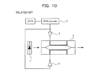
- FIG. 10 illustrates an optical transmitter based on a DPSK modulation scheme used for an optical transmission network using such a phase modulation scheme.
- the optical transmitter illustrated in FIG. 10 has a configuration in which CW (Continuous Wave) light output from a semiconductor laser 1 is phase-modulated through a Mach-Zehnder type optical phase modulator 2 and transmitted as an optical signal.
- the optical phase modulator 2 outputs a phase-modulated optical signal using a drive signal output from a driver 4 according to a data signal that has passed through a DPSK precoder 3 , and the mechanism thereof is shown in FIG. 11 .
- a Mach-Zehnder type optical waveguide 21 is formed in an electro-optical crystal substrate 20 represented by LiNbO 3 (hereinafter referred to as “LN”) and traveling wave electrodes 22 and 23 are formed on the surface of the substrate 20 .
- LN electro-optical crystal substrate 20 represented by LiNbO 3
- the optical waveguide 21 is a Mach-Zehnder type optical waveguide including an input section that faces a substrate end face for inputting light, branch modulation sections (arms) that branch and extend from the input section and an output section that combines the branch modulation sections and faces a substrate end face.
- branch modulation sections armss
- output section that combines the branch modulation sections and faces a substrate end face.
- the drive signal output from the driver 4 causes the one electrode 22 to vary from 0 to V ⁇ and causes the other electrode 23 to vary from 0 to ⁇ V ⁇ , and can thereby perform optical phase modulation of phase 0, ⁇ (e.g., non-Patent Document “40-Gb/s RZ-Differential Phase Shift Keyed Transmission”, A. Gnauck, ThE1, pp. 450-451, Vol. 2, OFC 2003).
- a Mach-Zehnder type optical modulator includes an optical waveguide formed in an electro-optical substrate, an input section that inputs light to the optical waveguide, a plurality of branch modulation sections that generate branched input light, extend from the input section and modulate the branched input light, an interference photocoupler including a plurality of input ports and a plurality of output ports, the input ports being coupled to the branch modulation sections, and an output photocoupler including a plurality of input ports coupled to the output ports of the interference photocoupler and also including a plurality of output ports.
- a Mach-Zehnder type optical modulator including an optical waveguide formed in an electro-optical substrate, an input photocoupler including a plurality of input ports that are configured to input light to the optical waveguide and a plurality of output ports, a plurality of branch modulation sections that generate branched input light, extend from the output ports of the input photocoupler section and modulate the branched input light, an interference photocoupler section including a plurality of input ports and a plurality of output ports, the input ports being coupled to the branch modulation section, and an output photocoupler section including a plurality of input ports coupled to the output ports of the interference photocoupler section and also including one output port.
- FIG. 1A and FIG. 1B illustrate an optical phase relationship between input ports and output ports of a 2 ⁇ 2 photocoupler
- FIG. 2A and FIG. 2B illustrate an optical phase relationship between input ports and an output port of a 2 ⁇ 1 photocoupler
- FIG. 3A , FIG. 3B , FIG. 3C , and FIG. 3D illustrate a plan view and phase variations showing a Mach-Zehnder type optical modulator according to a first embodiment
- FIG. 4 illustrates phase variations of light of the Mach-Zehnder type optical modulator according to the first embodiment as mathematical expressions
- FIG. 5A illustrates a plan view of a Mach-Zehnder type optical modulator according to a second embodiment
- FIG. 5B illustrates a plan view of a Mach-Zehnder type optical modulator according to a third embodiment
- FIG. 6A , FIG. 6B , FIG. 6C , FIG. 6D , and FIG. 6E illustrate phase variations of light in the Mach-Zehnder type optical modulator according to the second and third embodiments;
- FIG. 7 illustrates phase variations of light in the Mach-Zehnder type optical modulator according to the second and third embodiments as mathematical expressions
- FIG. 8 illustrates a plan view of a Mach-Zehnder type optical modulator according to a fourth embodiment
- FIG. 9 illustrates a plan view of a Mach-Zehnder type optical modulator according to a fifth embodiment
- FIG. 10 illustrates a block diagram of an optical transmitter according to a prior art
- FIG. 11A and FIG. 11B illustrate a plan view and phase variations of a Mach-Zehnder type optical modulator according to the prior art.
- FIG. 12A and FIG. 12B illustrate a plan view of another Mach-Zehnder type optical modulator according to the prior art.
- FIG. 1A and FIG. 1B illustrate a phase relationship between incident light and emerging light of a photocoupler having two inputs ⁇ two outputs as an example of a photocoupler section provided for the optical waveguide proposed above.
- FIG. 2A and FIG. 2B illustrate a phase relationship between incident light and emerging light of a photocoupler having two inputs ⁇ one output.
- incident light beams A and B that impinge upon two input ports are coupled and output from an output port, and therefore no phase shift occurs in an emerging light beam C ( FIG. 2B ) with respect to the incident light beams A and B.
- incident light beams A and B that impinge upon two input ports interfere with each other and are then output from two output ports, and therefore phase shifts of ⁇ /4 occur in emerging light beams C and D with respect to the incident light beams A and B. This is because the incident light and emerging light in the 2 ⁇ 2 photocoupler as shown in FIG.
- FIGS. 3A-3D illustrate a Mach-Zehnder type optical modulator of the present embodiment using this phase relationship.
- the optical modulator uses a Z-cut LN substrate 100 as an electro-optical crystal substrate and a Mach-Zehnder type optical waveguide 101 is formed in the substrate 100 .
- the optical waveguide 101 is provided with an input section 102 that faces one end face of the substrate 100 and two branch modulation sections 103 and 104 that branch and extend in parallel from the input section 102 .
- An interference photocoupler section 105 having two inputs ⁇ two outputs is provided and has input ports that are coupled to the branch modulation sections 103 and 104 respectively.
- an output photocoupler section 106 having two inputs ⁇ two outputs is provided and has input ports that are coupled to the two output ports of the interference photocoupler section 105 and whose output ports face the other end face of the substrate 100 .
- An output optical signal can be obtained from one of the output ports of the output photocoupler section 106 .
- the modulated light beams that have passed through the branch modulation sections 103 and 104 are input to the input ports of the interference photocoupler section 105 , which constitutes a 2 ⁇ 2 photocoupler as shown in FIGS. 1A and 1B . Therefore, phase shifts of ⁇ /4 are produced in interference light beams (which correspond to C and D in FIGS. 1A and 1B ) output from the output ports of the interference photocoupler section 105 with respect to the modulated light beams (which correspond to A and B in FIGS. 1A and 1B ) of the branch modulation sections 103 and 104 .
- the interference light beams output from the interference photocoupler section 105 are input to the input ports of the output photocoupler section 106 , respectively. Since the output photocoupler section 106 also constitutes a 2 ⁇ 2 photocoupler as shown in FIG. 1A , phase shifts of ⁇ /4 are produced in output light beams (which correspond to C and D in FIGS. 1A and 1B ) output from the output ports with respect to the interference light beams (which correspond to A and B in FIGS. 1A and 1B ) input to the input ports.
- One traveling wave electrode 107 is formed on the surface of the substrate 100 in order to change the refractive index of the optical waveguide of the one branch modulation section 103 with respect to the branch modulation sections 103 and 104 in the optical waveguide 101 formed in the substrate 100 .
- the traveling wave electrode 107 illustrated here is formed so as to superimpose on the branch modulation section 103 , receives a drive signal from the driver as shown, for example, in FIG. 10 and applies an electric field to the branch modulation section 103 .
- the drive signal applied to the traveling wave electrode 107 can apply optical phase modulation of phase 0, ⁇ according to a data signal with a voltage variation from 0 to V ⁇ when a voltage that causes the optical phase difference between the branch modulation sections 103 and 104 to be a half wavelength is V ⁇ .
- phase modulation of ⁇ (0 to ⁇ ) when phase modulation of ⁇ (0 to ⁇ ) is applied only to the modulated light of the one branch modulation section 103 , a phase shift occurs when the light passes through the interference photocoupler section 105 and the output photocoupler section 106 , and phase modulation of ⁇ (0 to ⁇ ) appears in the output light. That is, according to the optical waveguide 101 of the present embodiment, changing the voltage of the drive signal applied to the one traveling wave electrode 107 from 0 to V ⁇ allows phase modulation of phase 0, ⁇ to be added to the output light output from the output photocoupler section 106 . As shown in the expressions in FIG.
- the voltage of the drive signal requires 0 to 2V ⁇ in a single drive scheme and 0 to V ⁇ and 0 to ⁇ V ⁇ in a dual drive scheme.
- the voltage required for the drive signal is only 0 to V ⁇ under a single drive scheme, that is, half the level of the prior art.
- the output port of the output photocoupler section 106 from which output light is extracted in the illustrated optical waveguide 101 is selected depending on which output light with a positive phase or opposite phase is obtained.
- the photocoupler section is also applicable to a case where the input section is branched into three or more branch modulation sections.
- the photocoupler section is also applicable to a multi-value modulation scheme such that the respective branch modulation sections branched from the input section are further branched.
- FIG. 5A and FIG. 5B illustrate other embodiments of a Mach-Zehnder type optical modulator provided with a traveling wave electrode under a single drive scheme.
- FIG. 5A is an embodiment using an X-cut LN substrate and
- FIG. 5B is an embodiment using a Z-cut LN substrate.
- phase modulated output light is obtained from the output port of the output photocoupler section 206 .
- a traveling wave electrode 207 is formed on the substrate surface so as to extend at an intermediate position between the branch modulation sections 203 and 204 and two grounding electrodes 208 and 209 , spaced apart from each other by a predetermined distance, extend along both sides of the traveling wave electrode 207 .
- the refractive indices of the optical waveguides of the branch modulation sections 203 and 204 vary according to electric fields produced between the traveling wave electrode 207 and the grounding electrodes 208 and 209 .
- an optical waveguide 301 formed in an LN substrate 300 has the same structure as that of the optical waveguide 201 in FIG. 5A , and is provided with an input photocoupler section 302 having two inputs ⁇ two outputs as an input section, input ports of which face one end face of the substrate 300 .
- Branch modulation sections 303 and 304 extend from the output ports of the input photocoupler section 302 and two input ports of an interference photocoupler section 305 having two inputs ⁇ two outputs are coupled to the branch modulation sections 303 and 304 .
- Two output ports of the interference photocoupler section 305 are coupled to input ports of an output photocoupler section 306 having two inputs ⁇ one output and the one output port of the output photocoupler section 306 faces the other end face of the substrate 300 .
- phase modulated output light is also obtained from the output port of the output photocoupler section 306 .
- a polarization inversion region 307 is formed in part of the area where the branch modulation sections 303 and 304 are formed in the substrate 300 having such an optical waveguide 301 .
- One traveling wave electrode 308 extends on the substrate 300 so as to superimpose on the one branch modulation section 303 outside the polarization inversion region 307 and superimpose on the other branch modulation section 304 inside the polarization inversion region 307 . That is, the traveling wave electrode 308 extends in a stepped shape so as to change the refractive index of the optical waveguide of the different branch modulation sections 303 and 304 inside and outside the polarization inversion region 307 .
- FIGS. 6A-6E illustrate phase shifts in the embodiments shown in FIG. 5A and FIG. 5B and FIG. 7 illustrates the mathematical expressions thereof.
- the phase shifts of ⁇ /4 explained in FIG. 1 are produced between the light propagating through the one branch modulation section 203 or 303 and the light propagating through the other branch modulation section 204 or 304 at first.
- modulated light for adding phase modulation ⁇ (0 to ⁇ /2, 0 to ⁇ /2) to the light through the branch modulation section 203 or 303 , and branch modulation section 204 or 304 is input to the interference photocoupler section 205 or 305 the phase shifts of ⁇ /4 explained in FIG. 1A and FIG.
- phase modulation of phase 0, ⁇ appears in the output light. That is, when a voltage which causes the optical phase difference between the branch modulation sections 203 or 303 , and 204 or 304 to be a half wavelength is V ⁇ , if the voltage of the drive signal applied to the traveling wave electrode 207 or 308 is made to change from 0 to V ⁇ , optical phase modulation of phase 0, ⁇ according to a data signal can be added.
- FIG. 8 illustrates an embodiment based on a dual drive scheme.
- an optical waveguide 401 similar to that of the embodiments in FIG. 5A and FIG. 5B is formed in a Z-cut LN substrate 400 . That is, the optical waveguide 401 is provided with an input photocoupler section 402 having two inputs ⁇ two outputs, branch modulation sections 403 and 404 that extend from the output ports thereof, an interference photocoupler section 405 having two inputs ⁇ two outputs whose input ports are coupled to the branch modulation sections 403 and 404 and an output photocoupler section 406 having two inputs ⁇ one output whose input ports are coupled to the output ports of the interference photocoupler section 405 .
- a total of two traveling wave electrodes 407 and 408 are disposed on the substrate so as to superimpose on the branch modulation sections 403 and 404 respectively to change the refractive indices of the optical waveguides of the branch modulation sections 403 and 404 .
- FIG. 9 illustrates an embodiment in which part of interference light that has passed through an interference photocoupler section is extracted and monitored, and feedback is given to the driver (see FIG. 10 ) based on the monitoring result to thereby allow drive signals to be controlled.
- An optical waveguide 501 similar to that of the embodiment in FIG. 3A is formed in an LN substrate 500 . That is, the optical waveguide 501 illustrated in FIG. 9 includes an input section 502 to input light that faces a substrate end face, branch modulation sections 503 and 504 that are branched into two portions and extend in parallel from the input section 502 , an interference photocoupler section 505 having two inputs ⁇ two outputs whose input ports are coupled to the branch modulation sections 503 and 504 , respectively, and an output photocoupler section 506 having two inputs ⁇ two outputs whose input ports are coupled to the output ports of the interference photocoupler section 505 , respectively.
- the output ports of the output photocoupler section 506 face the end face of the substrate 500 .
- the mode of the optical waveguide is not limited to this and an optical waveguide similar to that in the embodiments in FIG. 5A and FIG. 5B or the like may also be used.
- a traveling wave electrode 507 formed on the substrate 500 is a single drive scheme formed so as to be superimposed on the one branch modulation section 503 .
- the drive signal (0 to V ⁇ ) explained above is applied to the traveling wave electrode 507 , and phase modulation of phase 0, ⁇ is thereby given to the output light.
- part of interference light is extracted from the output ports of the interference photocoupler section 505 to photodiodes 512 and 513 through monitoring waveguides 510 and 511 formed in the substrate 500 .
- the photodiodes 512 and 513 are also built in the substrate 500 .
- Electric monitoring signals output after being photoelectrically converted by the photodiodes 512 and 513 are supplied to a monitor 514 that is an electric circuit and the monitor 514 gives feedback to a driver 515 according to the monitoring result obtained by the monitoring signals. In this way, the period and voltage or the like of the drive signal output from the driver 515 are controlled.
- the interference light after passing through the interference photocoupler section 505 has intensity modulation information
- using this as monitoring light for control provides an advantage that the optical phase modulator can be easily controlled.
- the Mach-Zehnder type optical modulator can be provided with at least two photocoupler sections having a plurality of inputs ⁇ a plurality of outputs from an input end to an output end. Incident light beams are output after interfering with each other, and as a result, such a photocoupler has the nature that a phase shift occurs in emerging light. Using a phase shift occurring in the photocoupler allows a necessary optical phase variation to be obtained even if the voltage of a drive signal is low.
- a photocoupler section is appropriately provided in the optical waveguide, when a voltage which causes the optical phase difference between the branch modulation sections to be a half wavelength is V ⁇ , it is possible to perform optical phase modulation of phase 0, ⁇ according to a data signal through a voltage variation from 0 to V ⁇ for a drive signal applied to the traveling wave electrode under the above described single drive scheme.
- optical phase modulation of phase 0 can be performed according to a data signal through a voltage variation from 0 to V ⁇ /2 for a drive signal applied to each traveling wave electrode.
Abstract
Description
φM(mleft,mright)=(2π/M){mleft−(M+1)/2} {mright−(M+1)/2} (1)
Claims (11)
Applications Claiming Priority (2)
| Application Number | Priority Date | Filing Date | Title |
|---|---|---|---|
| JP2008208491A JP5239610B2 (en) | 2008-08-13 | 2008-08-13 | Mach-Zehnder optical modulator |
| JP2008-208491 | 2008-08-13 |
Publications (2)
| Publication Number | Publication Date |
|---|---|
| US20100040321A1 US20100040321A1 (en) | 2010-02-18 |
| US8023776B2 true US8023776B2 (en) | 2011-09-20 |
Family
ID=41681322
Family Applications (1)
| Application Number | Title | Priority Date | Filing Date |
|---|---|---|---|
| US12/536,880 Expired - Fee Related US8023776B2 (en) | 2008-08-13 | 2009-08-06 | Mach-Zehnder type optical modulator |
Country Status (2)
| Country | Link |
|---|---|
| US (1) | US8023776B2 (en) |
| JP (1) | JP5239610B2 (en) |
Cited By (1)
| Publication number | Priority date | Publication date | Assignee | Title |
|---|---|---|---|---|
| US20130182992A1 (en) * | 2011-12-12 | 2013-07-18 | Sumitomo Electric Industries, Ltd. | Method to drive semiconductor mach-zehnder modulator |
Citations (9)
| Publication number | Priority date | Publication date | Assignee | Title |
|---|---|---|---|---|
| US5249243A (en) * | 1992-05-21 | 1993-09-28 | Siemens Components, Inc. | Apparatus and method for cascade coupled integrated optical phase modulator for linearization of signal transfer |
| US5278923A (en) * | 1992-09-02 | 1994-01-11 | Harmonic Lightwaves, Inc. | Cascaded optical modulation system with high linearity |
| US6091864A (en) * | 1997-04-10 | 2000-07-18 | Ortel Corporation | Linear optical modulator for providing chirp-free optical signals |
| US20030021509A1 (en) * | 2001-05-03 | 2003-01-30 | Hrl Laboratories, Llc | Photonic encoding sampler |
| US20030147591A1 (en) * | 2002-02-07 | 2003-08-07 | Fujitsu Limited | Optical waveguide device and optical modulator |
| US20030219188A1 (en) * | 2002-05-15 | 2003-11-27 | Fujitsu Limited | Optical modulator, optical waveguide device and acousto-optic tunable filter apparatus |
| US20040101227A1 (en) * | 2001-06-29 | 2004-05-27 | Masakazu Takabayashi | Polarization dispersion compensating apparatus |
| US6760493B2 (en) * | 2001-06-28 | 2004-07-06 | Avanex Corporation | Coplanar integrated optical waveguide electro-optical modulator |
| US20060133713A1 (en) * | 2000-03-15 | 2006-06-22 | Manabu Yamada | Optical waveguide modulator equipped with an output light monitor |
Family Cites Families (2)
| Publication number | Priority date | Publication date | Assignee | Title |
|---|---|---|---|---|
| JP4594744B2 (en) * | 2005-01-14 | 2010-12-08 | 富士通オプティカルコンポーネンツ株式会社 | Optical communication device and optical device |
| JP2007114307A (en) * | 2005-10-18 | 2007-05-10 | Fujitsu Ltd | Chirp-switching circuit and optical transmission system |
-
2008
- 2008-08-13 JP JP2008208491A patent/JP5239610B2/en not_active Expired - Fee Related
-
2009
- 2009-08-06 US US12/536,880 patent/US8023776B2/en not_active Expired - Fee Related
Patent Citations (9)
| Publication number | Priority date | Publication date | Assignee | Title |
|---|---|---|---|---|
| US5249243A (en) * | 1992-05-21 | 1993-09-28 | Siemens Components, Inc. | Apparatus and method for cascade coupled integrated optical phase modulator for linearization of signal transfer |
| US5278923A (en) * | 1992-09-02 | 1994-01-11 | Harmonic Lightwaves, Inc. | Cascaded optical modulation system with high linearity |
| US6091864A (en) * | 1997-04-10 | 2000-07-18 | Ortel Corporation | Linear optical modulator for providing chirp-free optical signals |
| US20060133713A1 (en) * | 2000-03-15 | 2006-06-22 | Manabu Yamada | Optical waveguide modulator equipped with an output light monitor |
| US20030021509A1 (en) * | 2001-05-03 | 2003-01-30 | Hrl Laboratories, Llc | Photonic encoding sampler |
| US6760493B2 (en) * | 2001-06-28 | 2004-07-06 | Avanex Corporation | Coplanar integrated optical waveguide electro-optical modulator |
| US20040101227A1 (en) * | 2001-06-29 | 2004-05-27 | Masakazu Takabayashi | Polarization dispersion compensating apparatus |
| US20030147591A1 (en) * | 2002-02-07 | 2003-08-07 | Fujitsu Limited | Optical waveguide device and optical modulator |
| US20030219188A1 (en) * | 2002-05-15 | 2003-11-27 | Fujitsu Limited | Optical modulator, optical waveguide device and acousto-optic tunable filter apparatus |
Non-Patent Citations (2)
| Title |
|---|
| Doerr, C.R., et al., "Monolithic Demodulator for 40-gb/s DQPSK Using a Star Coupler", Journal of Lightwave Technology, vol. 24, No. 1, Jan. 2006, pp. 171-174. |
| Gnauck, A., "40-Gb/s RZ-Differential Phase Shift Keyed Transmission", ThE1, vol. 2, OFC 2003, pp. 450-451. |
Cited By (2)
| Publication number | Priority date | Publication date | Assignee | Title |
|---|---|---|---|---|
| US20130182992A1 (en) * | 2011-12-12 | 2013-07-18 | Sumitomo Electric Industries, Ltd. | Method to drive semiconductor mach-zehnder modulator |
| US9298024B2 (en) * | 2011-12-12 | 2016-03-29 | Sumitomo Electric Industries, Ltd. | Semiconductor Mach-Zender modulator and method to drive the same |
Also Published As
| Publication number | Publication date |
|---|---|
| JP2010044236A (en) | 2010-02-25 |
| JP5239610B2 (en) | 2013-07-17 |
| US20100040321A1 (en) | 2010-02-18 |
Similar Documents
| Publication | Publication Date | Title |
|---|---|---|
| US8849071B2 (en) | Optical waveguide modulator | |
| US8705900B2 (en) | Optical modulator | |
| JP5069144B2 (en) | Light modulator | |
| US9081216B2 (en) | Optical device having optical modulators | |
| US8374467B2 (en) | Optical device having a plurality of Mach-Zehnder modulators | |
| US7826689B2 (en) | Optical device which outputs independently modulated light beams in respective TE and TM polarization modes | |
| US9568801B2 (en) | Optical modulator | |
| US9703169B2 (en) | Optical modulator | |
| US6341031B1 (en) | Optical pulse generation using a high order function waveguide interferometer | |
| JP2009003247A (en) | Optical waveguide device | |
| US20100067841A1 (en) | Optical device and optical transmitter | |
| US9423566B2 (en) | Optical modulator and optical transmitter | |
| US20090162014A1 (en) | Optical waveguide device and optical apparatus using optical waveguide device | |
| JP5594192B2 (en) | Light modulator | |
| US9298024B2 (en) | Semiconductor Mach-Zender modulator and method to drive the same | |
| US20090067852A1 (en) | Optical modulator and optical transmitter | |
| US8023776B2 (en) | Mach-Zehnder type optical modulator | |
| JP6385848B2 (en) | Light modulator | |
| EP2659602B1 (en) | An optical duobinary modulated signal generator | |
| US11852878B2 (en) | Optical device and optical communication apparatus | |
| Tyagi et al. | A Review on Optical Modulators Used in Radio Over Fiber (RoF) System for 6G IoT Applications | |
| JP6106062B2 (en) | Light modulator |
Legal Events
| Date | Code | Title | Description |
|---|---|---|---|
| AS | Assignment |
Owner name: FUJITSU LIMITED,JAPAN Free format text: ASSIGNMENT OF ASSIGNORS INTEREST;ASSIGNOR:TSUNODA, YUKITO;REEL/FRAME:023080/0959 Effective date: 20090709 Owner name: FUJITSU LIMITED, JAPAN Free format text: ASSIGNMENT OF ASSIGNORS INTEREST;ASSIGNOR:TSUNODA, YUKITO;REEL/FRAME:023080/0959 Effective date: 20090709 |
|
| STCF | Information on status: patent grant |
Free format text: PATENTED CASE |
|
| FEPP | Fee payment procedure |
Free format text: PAYOR NUMBER ASSIGNED (ORIGINAL EVENT CODE: ASPN); ENTITY STATUS OF PATENT OWNER: LARGE ENTITY |
|
| FPAY | Fee payment |
Year of fee payment: 4 |
|
| FEPP | Fee payment procedure |
Free format text: MAINTENANCE FEE REMINDER MAILED (ORIGINAL EVENT CODE: REM.); ENTITY STATUS OF PATENT OWNER: LARGE ENTITY |
|
| LAPS | Lapse for failure to pay maintenance fees |
Free format text: PATENT EXPIRED FOR FAILURE TO PAY MAINTENANCE FEES (ORIGINAL EVENT CODE: EXP.); ENTITY STATUS OF PATENT OWNER: LARGE ENTITY |
|
| STCH | Information on status: patent discontinuation |
Free format text: PATENT EXPIRED DUE TO NONPAYMENT OF MAINTENANCE FEES UNDER 37 CFR 1.362 |
|
| FP | Lapsed due to failure to pay maintenance fee |
Effective date: 20190920 |