US8027651B2 - Method and apparatus for removing DC offset in a direct conversion receiver - Google Patents
Method and apparatus for removing DC offset in a direct conversion receiver Download PDFInfo
- Publication number
- US8027651B2 US8027651B2 US12/329,034 US32903408A US8027651B2 US 8027651 B2 US8027651 B2 US 8027651B2 US 32903408 A US32903408 A US 32903408A US 8027651 B2 US8027651 B2 US 8027651B2
- Authority
- US
- United States
- Prior art keywords
- dcoc
- algorithm
- algorithms
- signal quality
- signal
- Prior art date
- Legal status (The legal status is an assumption and is not a legal conclusion. Google has not performed a legal analysis and makes no representation as to the accuracy of the status listed.)
- Active, expires
Links
- 238000000034 method Methods 0.000 title claims abstract description 42
- 238000006243 chemical reaction Methods 0.000 title claims abstract description 31
- 238000012937 correction Methods 0.000 claims abstract description 62
- 230000007704 transition Effects 0.000 claims abstract description 28
- 238000012545 processing Methods 0.000 claims description 17
- 238000012935 Averaging Methods 0.000 claims description 12
- 230000003213 activating effect Effects 0.000 claims description 3
- 230000002093 peripheral effect Effects 0.000 claims description 3
- 230000009977 dual effect Effects 0.000 abstract description 2
- 239000000523 sample Substances 0.000 description 19
- 238000001914 filtration Methods 0.000 description 18
- 230000010354 integration Effects 0.000 description 18
- 238000010586 diagram Methods 0.000 description 16
- 230000004044 response Effects 0.000 description 11
- 230000008901 benefit Effects 0.000 description 8
- 230000008569 process Effects 0.000 description 8
- 238000013459 approach Methods 0.000 description 7
- 230000008859 change Effects 0.000 description 7
- 230000001960 triggered effect Effects 0.000 description 6
- 238000004364 calculation method Methods 0.000 description 5
- 230000006870 function Effects 0.000 description 5
- 238000007493 shaping process Methods 0.000 description 4
- 230000007613 environmental effect Effects 0.000 description 3
- 239000000470 constituent Substances 0.000 description 2
- 238000005562 fading Methods 0.000 description 2
- 238000012986 modification Methods 0.000 description 2
- 230000004048 modification Effects 0.000 description 2
- 238000013139 quantization Methods 0.000 description 2
- 230000001360 synchronised effect Effects 0.000 description 2
- 230000009471 action Effects 0.000 description 1
- 230000004913 activation Effects 0.000 description 1
- 230000003044 adaptive effect Effects 0.000 description 1
- 230000003466 anti-cipated effect Effects 0.000 description 1
- 238000004891 communication Methods 0.000 description 1
- 230000008878 coupling Effects 0.000 description 1
- 238000010168 coupling process Methods 0.000 description 1
- 238000005859 coupling reaction Methods 0.000 description 1
- 230000003111 delayed effect Effects 0.000 description 1
- 238000013461 design Methods 0.000 description 1
- 238000001514 detection method Methods 0.000 description 1
- 230000001627 detrimental effect Effects 0.000 description 1
- 238000005516 engineering process Methods 0.000 description 1
- 230000000116 mitigating effect Effects 0.000 description 1
- 238000012805 post-processing Methods 0.000 description 1
- 230000001052 transient effect Effects 0.000 description 1
Images


Classifications
-
- H—ELECTRICITY
- H04—ELECTRIC COMMUNICATION TECHNIQUE
- H04B—TRANSMISSION
- H04B1/00—Details of transmission systems, not covered by a single one of groups H04B3/00 - H04B13/00; Details of transmission systems not characterised by the medium used for transmission
- H04B1/06—Receivers
- H04B1/16—Circuits
- H04B1/30—Circuits for homodyne or synchrodyne receivers
-
- H—ELECTRICITY
- H04—ELECTRIC COMMUNICATION TECHNIQUE
- H04L—TRANSMISSION OF DIGITAL INFORMATION, e.g. TELEGRAPHIC COMMUNICATION
- H04L25/00—Baseband systems
- H04L25/02—Details ; arrangements for supplying electrical power along data transmission lines
- H04L25/06—Dc level restoring means; Bias distortion correction ; Decision circuits providing symbol by symbol detection
- H04L25/061—Dc level restoring means; Bias distortion correction ; Decision circuits providing symbol by symbol detection providing hard decisions only; arrangements for tracking or suppressing unwanted low frequency components, e.g. removal of dc offset
Definitions
- This invention relates generally to direct conversion receiver systems, and more specifically to direct current (DC) offset correction of baseband signals in direct conversion receiver systems.
- RF signals received by a direct conversion receiver are often converted into an in-phase (I) component and a quadrature (Q) component.
- I in-phase
- Q quadrature
- the direct conversion receiver converts the incoming signal to baseband by mixing it with a Local Oscillator (LO) signal having a frequency that is approximately equal to the carrier frequency of the desired on channel signal.
- LO Local Oscillator
- I/Q mismatch and intrinsic LO self-mixing may introduce a DC offset error.
- information modulated onto a received RF signal that is equal in frequency to the LO signal is mixed down to DC voltage within the baseband intermediate frequency (IF) signals.
- IF intermediate frequency
- This modulated information may be corrupted by intrinsic baseband DC offset errors inherent in stages constituent to the analog baseband signal path including the down conversion mixer, post mixer filtering and gain stages. These errors degrade signal quality. For instance, reverse-transmission paths may occur in a direct conversion receiver that may allow LO energy to couple into the mixer's RF input signal path.
- the LO energy at the RF input signal path may self-mix with the LO injected into the mixer and create DC offset errors proportional to the LO coupling into the RF path, thereby affecting signal reception.
- detection and correction of DC offset errors is important to improved signal reception.
- FIG. 1 is a block diagram of an exemplary direct conversion receiver.
- FIG. 2 is a block diagram of an exemplary digital filtering and formatting component of the direct conversion receiver.
- FIG. 3 is a flow chart illustrating an exemplary method for correcting DC offset error through the use of a plurality of DC offset correction algorithms.
- FIG. 4 is an example state machine diagram illustrating DC offset correction algorithm selection.
- FIG. 5 illustrates an example recursive differentiate-integrate algorithmic block diagram with adaptive noise shaping.
- FIG. 6 illustrates an example minima-maxima algorithmic block diagram providing a dual DC averaging technique.
- FIG. 7 is a block diagram illustrating one example of DC offset correction threshold setting.
- FIG. 8 illustrates an example transition between a differentiate-integrate algorithm to a minima-maxima algorithm for a DC correction weak signal threshold.
- FIG. 9 illustrates an example transition between a minima-maxima algorithm to an OFF state for a DC correction strong signal threshold.
- a DC offset correction (DCOC) component of the direct conversion receiver is adapted to select a DCOC algorithm from a plurality of DCOC algorithms as determined by a signal quality estimator component.
- the DCOC algorithms are configured to remove DC offset errors in baseband in-phase (I) and quadrature-phase (Q) signals received within a baseband signal path of the direct conversion receiver.
- the DCOC component controls transitioning between the DCOC algorithms and a DCOC OFF state based on set criterion for a signal quality estimate.
- the signal quality estimator component calculates signal quality estimates for use in selection and activation of a particular DCOC algorithm.
- DCOC compensation values are calculated with the DCOC algorithms.
- the DCOC component selects one of the DCOC algorithms using signal quality estimates as an indication of the receive operating environment.
- the DCOC algorithms are initialized with an initial seed state and the last DCOC compensation value previously obtained may be used as the initial seed state when transitioning from one DCOC algorithm to another DCOC algorithm.
- the DCOC component selects an initial DCOC compensation value during a first iteration period and parallel processes received I and Q samples by activating each of the DCOC algorithms.
- a thresholder of the DCOC component processes the signal quality estimate to select one of the DCOC algorithms.
- the selected DCOC algorithm determines a DCOC compensation value which is applied to the I and Q signals. Subsequently, another iteration period is triggered and a new DCOC compensation value is calculated using the selected DCOC algorithm.
- the DCOC component applies the new DCOC compensation value to the I and Q signals and the signal quality estimate is updated to reflect the current operating environment.
- An accumulator incorporated in the DCOC component may be used to integrate previous signal quality estimates with current signal quality estimates to produce an average estimate that is forwarded to the thresholder for processing. Based on input from the thresholder the DCOC component determines if the selected DCOC algorithm is to be maintained for continued application or if a different DCOC algorithm is to be activated. In one example embodiment, DCOC algorithm selection may be made between a differentiate-integrate algorithm and a minima-maxima algorithm.
- direct conversion receiver system 100 for processing RF signals.
- direct conversion receiver system 100 includes a receiver front end 102 , a mixer stage 104 , a post mixer filtering and formatting stage 106 , a digital signal processor 108 , a host controller 110 , and a frequency generation system 112 with associated voltage controlled oscillator (VCO) 114 .
- RF signals are received at antenna 116 and processed by receiver front end 102 which incorporates a filter stage 118 and a low noise amplifier (LNA) stage 120 .
- the output signal from receiver front end stage 102 is mainly composed of signals within a desired RF pass band, which is mixed with local oscillator (LO) signal 122 .
- the LO signal 122 is generated using frequency generation system 112 , containing frequency generation unit (FGU) 124 , loop filter 126 and VCO 114 as is well known in the art.
- FGU frequency generation unit
- the mixer stage 104 functions to frequency translate the received information to an intermediate frequency (IF) signal 128 for subsequent processing.
- the IF signal 128 can correspond to a very low IF (VLIF) frequency or a direct current (DC) baseband signal in which the LO frequency is approximately the same as the desired on channel frequency.
- VLIF very low IF
- DC direct current
- system 100 is said to operate with direct conversion receiver topology where the baseband DC voltage may contain desired receive information.
- the IF signal 128 may be subsequently processed by filtering and formatting stage 106 which contains low pass filter 130 , analog-to-digital converter (ADC) 132 to digitize the analog receive signal, and digital filtering and formatting component 134 .
- ADC analog-to-digital converter
- the output signal from filtering and formatting stage 106 may include a number of digital signals representative of the receive signal at receiver antenna 116 , which is subsequently processed by digital signal processor (DSP) 108 .
- DSP digital signal processor
- the DSP 108 recovers the desired information from the digital receive signal.
- the components of the direct conversion receiver system 100 may be configurable by host controller 110 using serial peripheral interface (SPI) signal 136 as is well known in the art.
- SPI serial peripheral interface
- the ADC 132 may be a Sigma Delta Modulator that converts complex in-phase (I) and quadrature phase (Q) analog input signals into a contiguous stream of samples whose values represent the amplitude and phase information of the analog input signals.
- the digital filtering and formatting component 134 containing various subcomponents adapted to post-process the ADC digital samples.
- the digital filtering and formatting component 134 may include a digital comb filter 210 to minimize aliasing distortion of the incoming samples, a variable decimator 212 to reduce the sample rate to a lower value and an Infinite Impulse Response (IIR) digital filter 214 to remove any DC offset error that may initially be present in the ADC input samples.
- the digital filtering and formatting component 134 may also contain a complex I/Q Finite Impulse Response (FIR) filter 216 to provide selectivity to undesired off-channel interference signals.
- a high resolution DC offset correction (DCOC) component 220 is provided and adapted to remove DC offset errors under different operating conditions while not distorting the desired modulated information that may be at DC.
- the final stage of digital filtering and formatting component 134 is a Synchronous Serial Interface (SSI) formatting component 280 that configures the input samples into a format that may be communicated and processed by a subsequent digital section such as DSP 108 .
- the SSI output samples may be communicated to the DSP 108 using a receive clock (RXCLK), receive data (RXD), and receive frame sync (RXFS) digital signals that are activated when the DSP 108 asserts a receive acquire (RXACQ) digital line.
- RXCLK receive clock
- RXD receive data
- RXFS receive frame sync
- the DCOC component 220 performs selection and transition of different DC offset correction algorithms.
- the DCOC component 220 FIG. 2
- SPI serial peripheral interface
- the DCOC component 220 may process I/Q samples continuously in real time for both the I and Q channels independently.
- the I and Q DC offset correction compensation values can be read back by the host processor 110 using the SPI 136 .
- the DC offset correction compensation values may be automatically applied to the I and Q channels. If an automatic mode is disabled at DCOC component 220 , the I/Q DC offset correction compensation value can be directly programmed using SPI 136 .
- the I/Q DCOC initial start-up time for DCOC component 220 may be synchronized with other processing triggers within the filtering and formatting component 134 , FIG. 2 .
- the DCOC component 220 may begin operation. This will avoid processing on transient samples.
- a logic indicator may be used to suspend processing of samples by the DCOC component 220 until a specific number of samples (time) has passed, after which DCOC component 220 will begin processing input samples from block 216 and apply the appropriate DC offset correction estimate.
- the DCOC component 220 may follow the I/Q FIR filter 216 within filtering and formatting component 134 .
- the relative position of DCOC component 220 need not be limited in this fashion, but may be located between any given block within filtering and formatting component 134 as may be necessary for accurate compensation of DC offset errors.
- FIG. 3 illustrates an exemplary overall DC offset correction state transition diagram that may be embodied in DCOC component 220 , FIG. 2 .
- An initial DC offset correction compensation value for state transition diagram 300 may originate from different system sources and may be selectable using SPI programming from the host controller 110 .
- the initial DC offset correction compensation value can be directly set using SPI as indicated in step 302 .
- the initial DCOC compensation value at DCOC start up can be derived from legacy DC offset correction strategies such as through IIR High Pass Filter (HPF) 214 in step 304 , or calculated using a mean estimator such as a customized seed averager 306 that may incorporate specialized fast response, variable length arithmetic mean routines.
- HPF IIR High Pass Filter
- the initial DC offset correction compensation value is applied as a beginning value for a first DCOC iteration period which is triggered in step 310 .
- step 310 parallel processing of the received I and Q samples begins with executing simultaneous iterations of any number of DCOC algorithms from a plurality of algorithm blocks 312 - 1 , 312 - 2 , through 312 -N.
- Each DCOC algorithm block 312 - 1 , 312 - 2 , through 312 -N operates independently on the I and Q channel sample data, with each DCOC algorithm being optimized for a particular receiver operating environment (e.g. signal strength level, attack time, modulation type, or other parametric variations).
- the DCOC algorithms within blocks 312 - 1 through 312 -N are initially executed in parallel after initial DCOC trigger block 310 because the receiver operating environment may initially be unknown. Once a signal quality estimate indicative of the operating environment is available, a specific DCOC compensation algorithm corresponding to the particular operating environment may be selected for continued operation. Additionally, signal quality estimates from the signal quality estimator component may be provided to the selected DCOC algorithm to further optimize performance for the current channel conditions. All other algorithms may be disabled to minimize battery power consumption.
- the signal quality estimator is an algorithmic process component that analyzes a signal to determine signal quality using one or more metrics. For instance, commonly used metrics such as power level, carrier to noise ratio, carrier to interferer ratio, fading channel characteristics and the like for gauging receive signal quality may be employed.
- the received signal may be an RF passband signal received at an antenna 116 , an IF signal 128 or a digitized I and Q sampled signal within digital filtering and formatting block 134 .
- the received signal may be comprised of a desired on-channel carrier, undesired off or on-channel interferers, thermal noise, and/or other sources.
- the signal quality estimate is generated by the signal quality estimator component and provides an estimate of signal quality.
- the signal quality estimator calculates a signal quality estimate that may be used in the selection of an optimal DCOC algorithm.
- signal quality estimate may be provided by signal quality estimator component 311 .
- the signal quality estimate can be one of, or a combination of, a plurality of metrics, including but not limited to Receive Signal Strength, Bit Error Rate, or Synchronization fidelity as is well known in the art.
- a Received Signal Strength Indicator (RSSI) calculation may be performed by signal quality estimator component 311 .
- the signal quality estimator component 311 need not be limited in this fashion.
- the signal quality estimator component 311 may generate any number of parameters used to select the optimum DCOC algorithm from the plurality of DCOC algorithms embedded in DCOC state transition 300 of DCOC component 220 .
- the output of signal quality estimator component 311 is connected to thresholder 314 .
- Thresholder 314 processes the signal quality estimate from signal quality estimator component 311 to produce the appropriate code word that may be used to select the optimal DCOC algorithm.
- the code word from thresholder 314 may be used to select the optimum algorithm from the plurality of DCOC algorithms 312 - 1 , 312 - 2 , through 312 -N.
- Step 318 also selects the DCOC compensation value derived from the optimum algorithm block as indicated by the code word from thresholder 314 .
- step 318 the appropriate compensation value is applied to the data in the I and Q channel independently in step 320 and a subsequent DC offset correction iteration period is triggered in step 322 .
- a new DCOC compensation value is calculated in step 324 using the DCOC algorithm which had previously been selected in step 318 .
- the compensation value derived in step 324 is applied to the I/Q sample stream in step 326 .
- the signal quality estimate is updated by signal quality estimator component 316 to reflect the current receive operating environment. For example, as seen in FIG. 3 , an updated RSSI calculation may be performed by the signal quality estimator component 316 . However, calculation of the signal quality estimate determined by signal quality estimator component 316 need not be limited in this fashion, since signal quality estimator component 316 may generate any number of parameters used to select the optimum DCOC algorithm from the plurality of DCOC algorithms embedded in DCOC state transition methodology 300 of DCOC component 220 . The updated RSSI calculated by signal quality estimator component 316 is subsequently forwarded to accumulator 330 .
- Accumulator 330 continuously integrates previous signal quality estimates with current signal quality estimates to produce an average value that can be post-processed by thresholder 331 .
- Thresholder 331 processes the signal quality estimate from accumulator 330 to produce the appropriate code word that may be used to update the active DCOC algorithm.
- the code word from thresholder 331 may be used in step 328 , to determine whether the current DCOC algorithm is optimally suited for the operating environment.
- step 328 of FIG. 3 the DCOC state transition 300 determines whether the active DCOC algorithm should be maintained or selection of a new algorithm is needed based on the input from thresholder 331 . If a DCOC algorithm change is required, an input value from thresholder 331 is used in step 332 to select the new DCOC algorithm from the plurality of DCOC algorithms embedded in the DCOC component 220 . After a new algorithm is selected that is optimal for the present receive channel operating environment, a new DCOC determination sequence may be triggered at step 334 . If no algorithm change is required, the output of decision step 328 bypasses the selection in step 332 to trigger a new DCOC determination period in step 334 .
- the active DCOC algorithm calculates the DCOC compensation value in step 336 and subsequently applies the compensation value in step 338 .
- the signal quality estimate is recalculated (e.g. updated RSSI) in signal quality estimator component 342 to indicate the present operating environment of the receive channel.
- the operating state of DCOC component 220 is determined in step 344 to ensure that continued processing of the DCOC compensation value is needed. If the DCOC state transition 300 of DCOC component 220 is enabled, then decision step 344 will update the accumulator block 330 with a new signal quality estimate obtained from signal quality estimator component 342 .
- Blocks 330 , 342 and 344 form a channel environmental metric loop that continuously calculates the signal quality estimate used to select the optimized algorithm selection.
- Blocks 328 , 332 , 334 , 336 , 338 and 340 form a parallel compensation loop that uses the environmental metric loop output to continuously match the DCOC algorithm that is being used to the operating environment. Updates to the signal quality estimate and changes to the DCOC compensation value can be accomplished sample-by-sample, or block-by-block which ever is best suited for the algorithm that is being utilized. Accumulator 330 may also incorporate a number of integration coefficients that allow for a number of system responses, including instantaneous changes in the selection metric or very slow, over damped variations.
- a method of correcting DC offset error of a received signal in a direct conversion receiver is provided.
- Different DCOC algorithms adapted to remove DC offset errors in a received signal within an I and Q baseband signal are employed at DCOC component 220 .
- Individual DCOC algorithms are selected from a plurality of DCOC compensation algorithms as determined by the signal quality estimator component. Criterion for signal quality estimates are set to control transitioning between various DCOC algorithms and a DC offset correction OFF state.
- the DCOC component 220 of direct conversion receiver 100 may select and transition between a duality of DCOC algorithms.
- a differentiate-integrate algorithm with quantization noise shaping
- a minima-maxima algorithm may be employed, in this example.
- the different DCOC algorithms are applied under different operating conditions. In this example, for instance, the differentiate-integrate algorithm may be applied at weaker signal levels and the minima-maxima algorithm may be applied at relatively strong signal levels.
- an exemplary state machine diagram 400 is shown illustrating an example of transition between a DC offset correction OFF state 410 , a differentiate-integrate algorithm 420 and a minima-maxima algorithm 430 .
- the received signal level is measured using a Received Signal Strength Indicator (RSSI) which may be used to select between the differentiate-integrate algorithm 420 and the minima-maxima algorithm 430 .
- RSSI Received Signal Strength Indicator
- the output signal from the receiver front end stage 102 is measured using one of several methods, as is well known in the art, to determine the on channel carrier power.
- This RSSI level is compared with a first threshold T 2 and if it is lower than the T 2 threshold, the differentiate-integrate algorithm 420 is selected.
- FIG. 5 is a block diagram that illustrates an example differentiate-integrate algorithm. Otherwise, the received signal level is compared with a second threshold T 4 , and if the RSSI is lower than the T 4 threshold, the minima-maxima algorithm 430 is selected.
- FIG. 6 is a block diagram that illustrates an example minima-maxima algorithm. Otherwise, no DC offset correction is utilized 410 .
- the differentiate-integrate algorithm 420 While the differentiate-integrate algorithm 420 is operational, the on channel received signal strength is compared with a third threshold T 1 , and if the RSSI is higher than the T 1 threshold, the minima-maxima algorithm 430 is selected, with the current DC estimate from the differentiate-integrate algorithm 420 being used to seed an initial starting value for the minima-maxima algorithm 430 to ensure a smooth transition. Otherwise, the differentiate-integrate algorithm 420 continues operating.
- the on channel received signal strength is compared to the first threshold T 2 , and if the RSSI is lower than the T 2 threshold, the differentiate-integrate algorithm 420 is selected (refer to FIG. 5 ), with the current DC estimate from the minima-maxima algorithm 430 used to seed an initial starting value for the differentiate-integrate algorithm 420 to ensure a smooth transition. Otherwise, the on channel receive signal strength is compared with a fourth threshold T 3 , and if the RSSI is higher than the T 3 threshold, the DC offset correction operation is terminated 410 . Otherwise, the minima-maxima algorithm 430 continues operating.
- initialization of the DCOC algorithms is performed to optimize initial DCOC compensation value accuracy and minimize DC transients that may be associated with transitions between algorithms.
- three different initial seed states may be used for initializing the DC offset correction algorithm. These seed states include: 1) setting the initial seed value as determined by a preceding IIR filtering block 304 ; 2) set initial seed state using a value derived from an initial I/Q DC seed averager 306 , FIG. 3 ; and 3) direct programming of the I/Q DC seed value using the SPI 302 . It should be noted that setting the I/Q DC seed state to zero may also be possible, but only if the DC error prior to the DCOC component 220 approaches zero.
- the seed averager 306 calculates an arithmetic mean for a specified number of samples, where the arithmetic mean is the sum of the input samples divided by the number of samples.
- the number of initial samples used to determine the initial seed value may be set by SPI 136 .
- DCOC component 220 two (2) DC offset correction algorithms are incorporated into the DCOC component 220 ; a differentiate-integrate algorithm and a minima-maxima algorithm.
- DCOC component 220 need not be limited in this fashion, but may incorporate any number of a plurality of DCOC algorithms that are known in the art.
- the number of samples processed by an algorithm to determine a DCOC compensation value may vary depending on algorithmic requirements.
- Algorithmic applicability need not be limited in requiring that all algorithms within DCOC component 220 be equal, or that the DCOC compensation update occur after each block (block by block update) or after each sample (sample by sample update) as is well known in the art.
- the algorithms may be optimized to provide different advantages at different RF operating environments. For the embodiment illustrated in FIG.
- the individual algorithms are threshold selectable based on input signal level as measured by RSSI.
- a status logic signal may become available to the SSI formatting component 222 to communicate to processing blocks 108 and 110 of FIG. 1 which particular DCOC algorithm is being utilized and the current operating status of the DCOC component 220 .
- a status logic indicator may be used to indicate over SSI signals the DCOC algorithm status on a per sample basis. This information may be used by the DSP 108 or host processor 110 for post processing the input samples.
- the differentiate-integrate algorithm estimates of the DCOC compensation values for the I and Q channel baseband signals are calculated independently.
- the operating state of the DCOC component 220 is defined by the signal quality estimator component 342 of FIG. 3 , which may include the received input signal level as indicated in a RSSI metric. If the RSSI is below a set threshold, the differentiate-integrate algorithm may be activated.
- FIG. 5 One possible embodiment of the differentiate-integrate algorithm is shown in FIG. 5 , incorporating a multiplierless implementation that may be optimally efficient for hardware realization.
- the differentiate-integrate algorithm illustrated in FIG. 5 also includes quantization noise shaping for improved fixed-point finite precision performance.
- I DC [n] and Q DC [n] are the DCOC compensation value estimates for the n th block of S samples for I and Q respectively, denoted by the complex discrete-time signal x[n].
- the operation Q 19 ⁇ . ⁇ means to quantize to 19-bits. Referring to FIG. 5 , a 19-bit quantized value of the compensated complex sample w[n] is subtracted from complex input same x[n] at summer 502 . The difference quantity y[n] is multiplied by integration scalar (1 ⁇ R) at block 506 where R is a real value greater than zero but less than 1.
- the product from multiplier 506 is summed with non-quantized compensated sample w[n] at summer 508 to produce a feed-forward summed output w[n+1].
- the output result of summer 508 is delayed by one sample at 510 to produce the dc complex sample w[n] to provide a feed-back path for summer 508 .
- Noise shaping is accomplished by quantizing w[n] at block 504 prior to summation at block 502 . It should be obvious to those skilled in the art that interim value y[n] represents the compensated input signal I[n] ⁇ I DC [n] and Q[n] ⁇ Q DC [n].
- the differentiate-integrate sequence runs sample-by-sample with an I and Q channel DCOC error compensation update occurring after a designated number of samples.
- the number of samples in each block of S samples may be defined in SPI.
- S may be two hundred, which in turn would define a block of S samples to be 10 mSec integration period assuming a 20 kilo-samples per second (ksps) input sample rate to the DCOC component 220 .
- the differentiate-integrate algorithm in this example may incorporate a sequence of three time periods, each having its own programmable integration factor R 1 , R 2 , and R 3 .
- integration factors R 1 and R 2 may have an associated number of blocks during which R 1 and R 2 is applied, designated as duration S 1 and S 2 respectively.
- a third iteration period associated with factor R 3 may be undefined, as it is assumed to be continuous following the first two periods.
- R 1 may be applied from 1 to S 1 blocks
- R 2 may be applied from S 1 +1 to S 2 blocks
- R 3 may be applied after S 2 blocks.
- the DCOC algorithm need not be limited in this fashion, but may incorporate any number of integration factors and associated integration periods as may be necessary for accurate compensation of DC offset errors.
- the integration factors may be partitioned into three ranges R 1 , R 2 , and R 3 , each of which may assume any value necessary to achieve the proper DC offset correction compensation value for a given time period.
- Range R 1 may be a very fast integration period to allow for fast changes for initial DC offset corrections.
- Range R 2 can assume an intermediate value and range R 3 can be set to a nominal slow decay integration period to minimize normal system fluctuations that would otherwise reduce DC offset correction compensation accuracy.
- the estimate for the k th block comprises taking the last estimate from the previous block and quantizing it to a number of bits, such as 19-bits, for example.
- the estimate from the previous block of samples is applied to the current block of samples.
- the estimate is applied by subtracting the estimate from the samples in that block.
- the differentiate-integrate sequence may run continuously until termination of processing by putting the direct conversion receiver 100 , FIG. 1 , into battery save, disabling the DCOC component 220 , FIG. 2 , or exceeding a predefined threshold as illustrated in FIG. 4 .
- a second approach for determining the I and Q channel DCOC compensation value uses a minima-maxima algorithm.
- the DCOC compensation value for the I and Q channels are calculated independently.
- the minima-maxima algorithm is applied when the DCOC component 220 is enabled and the received input signal level is between a pair of configurable thresholds.
- the DCOC compensation value may be calculated using a two-level averaging methodology that uses two successive averaging algorithms to determine the DCOC compensation value.
- the two-level averager may be employed to minimize the DC estimator variance.
- the two-level averaging strategy initially calculates the I and Q channel DC errors using the minima-maxima algorithm, where the maxima and minima are determined for a given block of S samples at block 602 and 604 respectively.
- the minima-maxima values are subsequently summed together at block 606 and divided by two (2) at block 608 to produce a DCOC compensation estimate.
- the DCOC compensation estimate at the output of block 608 can be expressed as:
- I D ⁇ ⁇ C min ⁇ ( I ) + max ⁇ ( I ) 2
- Q D ⁇ ⁇ C min ⁇ ( Q ) + max ⁇ ( Q ) 2
- min(.) and max(.) refer to the maxima and minima of sample values in a given block of S samples, respectively.
- the size of a block of S samples may be the same for both the minima-maxima algorithm and the differentiate-integrate algorithm. However, the block size S need not be limited in this fashion, but may any number of samples as may be necessary for accurate DCOC compensation determination.
- Each value of I DC and Q DC from block 608 may also be processed by a modified arithmetic averager composed of accumulator 612 and divider 614 .
- the modified accumulator 612 multiples each input DCOC compensation value from block 608 by a scalar value depending on the input from zero-crossing counter 610 .
- the zero crossing threshold block 610 may be used to ensure that the block of S samples used to calculate the minima-maxima DCOC compensation estimate contains a true minima and maxima value. To accomplish this, the zero-crossing counter 610 sets a minimum threshold of zero crossings that must be present in a given block of S samples to allow the DC estimate from block 608 to be multiplied by a unity scalar within accumulator block 612 .
- the minima-maxima DCOC compensation estimate from block 608 for that block of S samples may be multiplied by a scalar value less then one, or even zero (completely excluded) within accumulator block 612 . If the number of zero crossings is equal to or exceeding the threshold, then the minima-maxima DCOC compensation estimate from block 608 for that block of S samples is multiplied by one which allow the compensation estimate to be fully included in the accumulator summation at block 612 .
- the secondary modified averager system calculates the arithmetic mean of N DCOC compensation estimates I DC and Q DC .
- the secondary averager output can be arithmetically expressed as
- N is the number of I DC and Q DC estimates that have been accumulated from block 608 .
- the secondary averager may be bypassed if so configured through SPI.
- the output of the secondary averager is processed by a weighted average to determine the DCOC compensation value used to adjust the I and Q samples.
- the weighted average is accomplished in block 616 , 618 , 620 and 622 as is well known in the art.
- I DC [n] and Q DC [n] are the first averager output for the n th block of S samples for I and Q respectively, and Q 19 ⁇ . ⁇ in this example means to quantize to 19-bits.
- the number of samples used in each block and the block size for the differentiate-integrate and minima-maxima algorithms may be the same, but is not limited in this fashion.
- the block size for the differentiate-integrate algorithm and minima-maxima algorithm may be different and may be set to any value as may be required to achieve an accurate DCOC compensation value.
- the weighted averaging methodology for the minima-maxima algorithm may be the same as previously described for the differentiate-integrate algorithm.
- the minima-maxima averaging may incorporate a sequence of three time periods, each having its own programmable integration factor D 1 , D 2 , and D 3 , each having an associated number of blocks during which D 1 and D 2 is applied, designated as duration M 1 and M 2 respectively.
- a third iteration period associated with factor D 3 is undefined, as it is assumed to be continuous following the first two periods. Therefore, D 1 may be applied from 1 to M 1 blocks, D 2 may be applied from M 1 +1 to M 2 blocks, and D 3 may be applied after M 2 +1 blocks.
- the number of blocks may be defined in SPI.
- a 20 ksps samples rate at the input of DCOC component 220 and block size of 200 samples will result in an averaging period of 10 mS blocks. It is apparent to those skilled in the art that the averaging period will increase or decrease depending on the block size S, and the secondary averaging period will vary depending on the integration periods M 1 and M 2 . However, as will be appreciated by those skilled in the art that the differentiate-integrate DCOC algorithm need not be limited in this fashion, but may incorporate any number of integration factors and associated integration periods as may be necessary for accurate compensation of DC offset errors.
- the estimate for the k th block in this example consists of taking the last estimate from the previous block and quantizing it to 19-bits.
- the estimate from the previous block of samples is applied to the current block of samples.
- the estimate may be applied by subtracting the estimate from the samples in that block.
- the application of the estimate is separately enabled from the algorithm using SPI, so that the DC can be calculated but the estimate not applied if desired by the user.
- the minima-maxima sequence may run continuously until the termination of processing as in the differentiate-integrate algorithm.
- the integration factors may be scaled, for example, into three factors D 1 , D 2 , and D 3 , each of which may assume any value necessary to achieve the proper DC offset correction compensation value for a given time period.
- factor D 1 may be set to produce a fast DC compensation convergence with modest accuracy for integration period M 1
- factor D 2 may be set to produce a slower DC Compensation convergence with an intermediate accuracy for integration period M 2
- range D 3 may be set to produce the slowest DC compensation convergence with very high accuracy for integration period exceeding period M 2 .
- the minima-maxima sequence may run block-by-block with the I/Q DC offset correction update occurring continuously for every block of S samples until the termination of processing.
- the DC offset correction component 220 incorporates a threshold strategy for DC offset correction.
- Each of the different DC offset correction algorithms offer certain advantages in different operating environments.
- the DC offset correction component 220 is configurable to select which DC offset correction algorithm is used based on a set of thresholds. When transitioning from one DC offset correction algorithm to the next, the initial starting point from the new algorithm is seeded using the last value from the old algorithm. For example, switching to the integrate-differentiate algorithm from the minima-maxima algorithm, I est [0] and Q est [0] are seeded with the current minima-maxima estimate. Conversely, when switching to minima-maxima algorithm from the differentiate-integrate algorithm, Iest[0] and Qest[0] are seeded with the current differentiate-integrate estimate.
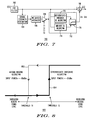
- FIG. 7 illustrates an example I/Q DC correction threshold.
- FIR filter 702 corresponds to the FIR filter 216 in FIG. 2 .
- the selection of the appropriate DCOC compensation algorithm is accomplished in selector block 710 .
- selector block 710 incorporates a differentiate-integrate algorithm block 712 , minima-maxima algorithm block 714 , and selection switch 716 .
- the selection switch 716 selects the algorithm that is to be used to accomplish the DCOC compensation that is applied to summer 718 .
- the algorithm selection at switch 716 is made based on thresholder 708 which incorporates a number of thresholds T 1 , T 2 , T 3 , and T 4 .
- the input to threshold block 708 is provided by weighted averager 706 .
- the weighted averager block 706 averages the input samples with a weighted averaging factor ⁇ as is well known in the art.
- the averaging block 706 receives an instantaneous receive signal strength (RSS) word (rss[n]) that may be based on a ⁇ square root over (I 2 +Q 2 ) ⁇ estimate or other level indicators such as Automatic Gain Control (AGC) attenuation settings which is provided by the I/Q signal strength estimator 704 .
- RSS receive signal strength
- AGC Automatic Gain Control
- the threshold system 700 may incorporate a weighted average capability to minimize instantaneous variations that may be present in the I and Q channel sampled receive signal.
- mag[n] and mag[n ⁇ 1] is the n and (n ⁇ 1) samples output from block 706 and rss[n] is the instantaneous receive signal strength word from block 704 .
- threshold system diagram 700 For simplicity, only one path is illustrated in threshold system diagram 700 ; however, the I and Q samples may be independently compensated using parallel compensation systems, where an individual compensation system is represent in FIG. 7 .
- complex time domain I/Q samples x[n] are filtered through the FIR filter 702 based on the filter configuration to generate the signal s[n].
- the transitions between DCOC algorithms is bounded by two (2) thresholds, in this example, to provide hysteresis for mitigating uncontrolled toggling between operating states.
- An example of threshold transitions for differentiate-integrate and minima-maxima algorithms are set forth below in Table 1.
- the thresholds defined in Table 1 may be one's compliment linear representation of the I or Q signal level.
- FIG. 8 illustrates an example transition response diagram between differentiate-integrate to minima-maxima DC offset correction algorithms. As seen in FIG. 8 , two thresholds T 1 and T 2 are implemented to allow hysteresis to be incorporated into the DCOC algorithm transitions. Hysteresis may be advantageous to prevent uncontrolled “toggling” between algorithms should the RSS become proximate with a particular threshold. As is well known in the art, real time variations of the received signal strength (RSS) are frequently encountered in RF receivers due to fading, multi-path phasing, or movement of surrounding objects such as vehicles.
- RSS received signal strength
- threshold response diagram 800 when the RSS is continuously below threshold T 2 , the DCOC compensation is calculated using the differentiate-integrate algorithm. If the RSS is continuously above threshold T 1 , the DCOC compensation is calculated using the minima-maxima algorithm. However, if changes in RSS cross threshold T 1 with the changes varying from weak signal to strong signal operating conditions as illustrated in response 802 of FIG. 8 , the DCOC compensation algorithm will change from differentiate-integrate to minima-maxima algorithm. In like manner if changes in RSS cross threshold T 2 with said changes varying from strong signal to weak signal operating conditions as illustrated in response 804 of FIG. 8 , the DCOC compensation algorithm will change from the minima-maxima to the differentiate-integrate algorithm.
- Thresholds T 1 and T 2 need not be equal; however, because more accurate DCOC compensation values may be realized using the differentiate-integrate algorithm for weak RSS conditions, threshold T 2 must be less than threshold T 1 for proper operation. As illustrated in the example in FIG. 8 , threshold T 1 may selectively correspond to an RSS of ⁇ 85 dBmm and threshold T 2 may selectively correspond to a RSS of ⁇ 95 dBm. These settings for T 1 and T 2 , in this example, will provide for 10 dB of hysteresis in the DCOC algorithm transition.
- FIG. 9 illustrates an example transition response diagram between minima-maxima DC offset correction algorithms to an DCOC OFF (or suspend) state. It is anticipated that the thresholds illustrated in FIG. 9 are higher than those shown in FIG. 8 , and may be independently controlled based on algorithm and receive environmental indicator metrics. As seen in FIG. 9 , two thresholds T 3 and T 4 are implemented to allow hysteresis to be incorporated into the DCOC algorithm transitions. When the RSS is continuously below threshold T 4 , the DCOC compensation is calculated using the minima-maxima algorithm. If the RSS is continuously above threshold T 3 , the DCOC compensation is calculated may be disabled or turned off.
- Thresholds T 3 and T 4 need not be equal; however, because more accurate DCOC compensation values may be realized using the minima-maxima algorithm for weaker RSS conditions, threshold T 4 must less than Threshold T 3 for proper operation.
- threshold T 3 may selectively correspond to an RSS of ⁇ 55 dBmm and threshold T 4 may selectively correspond to a RSS of ⁇ 65 dBm.
- DC offset correction compensation estimate is calculated but may not necessarily be applied if desired.
- Calculation and application of DC offset correction compensation are separate actions and the DC offset correction component may calculate the DC offset correction but selectively may not apply the correction value for various reasons (e.g. transients, muting the receive audio or other reasons).
Abstract
Description
I DC [n]=I DC [n−1]+(1−R)·(I[n]−Q 19 {I DC [n−1]})
and
Q DC [n]=Q DC [n−1]+(1−R)·(Q[n]−Q 19 {Q DC [n−1]})
I est [k]=Q 19 {I DC [n]}, Q est [k]=Q 19 {Q DC [n]}
-
- Arithmetic Mean ĪDC or
-
- where N=the number of DC estimates,
- kn=scalar value for sample block n,
- and xn=IDC or QDC for sample block n
Ī DC [n]=Ī DC [n−1]+(1−D)·(I[n]−Q 19 {Ī DC [n−1]})
and
where IDC[n] and QDC[n] are the first averager output for the nth block of S samples for I and Q respectively, and Q19{.} in this example means to quantize to 19-bits. In this example, the number of samples used in each block and the block size for the differentiate-integrate and minima-maxima algorithms may be the same, but is not limited in this fashion. The block size for the differentiate-integrate algorithm and minima-maxima algorithm may be different and may be set to any value as may be required to achieve an accurate DCOC compensation value.
I est [k]=Q 19 {I DC [n]}, Q est [k]=Q 19 {Q DC [n]}
The estimate for the kth block in this example consists of taking the last estimate from the previous block and quantizing it to 19-bits. The estimate from the previous block of samples is applied to the current block of samples. The estimate may be applied by subtracting the estimate from the samples in that block. The application of the estimate is separately enabled from the algorithm using SPI, so that the DC can be calculated but the estimate not applied if desired by the user. The minima-maxima sequence may run continuously until the termination of processing as in the differentiate-integrate algorithm.
mag[n]=α·mag[n−1]+(1−α)*rss[n]
| TABLE 1 | ||||
| PAST Algorithm | NEW Algorithm | Threshold | ||
| Diff-Int | max-min | T1 | ||
| Max-min | Diff-Int | T2 | ||
| Max-min | Strong signal OFF | T3 | ||
| Strong signal OFF | Max-min | T4 | ||
Claims (20)
Priority Applications (3)
| Application Number | Priority Date | Filing Date | Title |
|---|---|---|---|
| US12/329,034 US8027651B2 (en) | 2008-12-05 | 2008-12-05 | Method and apparatus for removing DC offset in a direct conversion receiver |
| PCT/US2009/064679 WO2010065281A2 (en) | 2008-12-05 | 2009-11-17 | Method and apparatus for removing dc offset in a direct conversion receiver |
| EP09830838.0A EP2374213B1 (en) | 2008-12-05 | 2009-11-17 | Method and apparatus for removing dc offset error in a direct conversion receiver |
Applications Claiming Priority (1)
| Application Number | Priority Date | Filing Date | Title |
|---|---|---|---|
| US12/329,034 US8027651B2 (en) | 2008-12-05 | 2008-12-05 | Method and apparatus for removing DC offset in a direct conversion receiver |
Publications (2)
| Publication Number | Publication Date |
|---|---|
| US20100144303A1 US20100144303A1 (en) | 2010-06-10 |
| US8027651B2 true US8027651B2 (en) | 2011-09-27 |
Family
ID=42231630
Family Applications (1)
| Application Number | Title | Priority Date | Filing Date |
|---|---|---|---|
| US12/329,034 Active 2030-04-02 US8027651B2 (en) | 2008-12-05 | 2008-12-05 | Method and apparatus for removing DC offset in a direct conversion receiver |
Country Status (3)
| Country | Link |
|---|---|
| US (1) | US8027651B2 (en) |
| EP (1) | EP2374213B1 (en) |
| WO (1) | WO2010065281A2 (en) |
Cited By (1)
| Publication number | Priority date | Publication date | Assignee | Title |
|---|---|---|---|---|
| US20110188616A1 (en) * | 2003-08-07 | 2011-08-04 | Panasonic Corporation | Radio transmitting apparatus and radio transmission method |
Families Citing this family (3)
| Publication number | Priority date | Publication date | Assignee | Title |
|---|---|---|---|---|
| US9048920B2 (en) | 2012-03-30 | 2015-06-02 | Motorola Solutions, Inc. | Method and apparatus for reducing FM audio artifacts in a receiver |
| US8787503B2 (en) * | 2012-09-18 | 2014-07-22 | Vixs Systems, Inc. | Frequency mixer with compensated DC offset correction to reduce linearity degradation |
| US9407477B2 (en) * | 2014-11-12 | 2016-08-02 | Motorola Solutions, Inc. | Method and apparatus for correlation canceller for interference mitigation with adaptive DC offset cancellation |
Citations (11)
| Publication number | Priority date | Publication date | Assignee | Title |
|---|---|---|---|---|
| US5212826A (en) | 1990-12-20 | 1993-05-18 | Motorola, Inc. | Apparatus and method of dc offset correction for a receiver |
| US5459679A (en) | 1994-07-18 | 1995-10-17 | Quantum Corporation | Real-time DC offset control and associated method |
| US6240100B1 (en) | 1997-07-31 | 2001-05-29 | Motorola, Inc. | Cellular TDMA base station receiver with dynamic DC offset correction |
| US6327313B1 (en) | 1999-12-29 | 2001-12-04 | Motorola, Inc. | Method and apparatus for DC offset correction |
| US6370205B1 (en) * | 1999-07-02 | 2002-04-09 | Telefonaktiebolaget Lm Ericsson (Publ) | Method and apparatus for performing DC-offset compensation in a radio receiver |
| US6449464B1 (en) * | 1999-12-28 | 2002-09-10 | Ericsson Inc. | Method of reporting signal quality measurements from a mobile terminal with enhanced demodulation algorithm |
| US6504884B1 (en) * | 1999-05-12 | 2003-01-07 | Analog Devices, Inc. | Method for correcting DC offsets in a receiver |
| US6639937B2 (en) * | 1999-09-30 | 2003-10-28 | Infineon Technologies Ag | Method and apparatus for producing spread-coded signals |
| US6785338B1 (en) * | 1999-01-19 | 2004-08-31 | Sarnoff Corporation | Constraining video production based on compression-related information |
| US7092464B2 (en) * | 2002-01-23 | 2006-08-15 | Bae Systems Information And Electronic Systems Integration Inc. | Multiuser detection with targeted error correction coding |
| US7624008B2 (en) * | 2001-03-13 | 2009-11-24 | Koninklijke Kpn N.V. | Method and device for determining the quality of a speech signal |
Family Cites Families (3)
| Publication number | Priority date | Publication date | Assignee | Title |
|---|---|---|---|---|
| US8559559B2 (en) * | 2002-06-20 | 2013-10-15 | Qualcomm, Incorporated | Method and apparatus for compensating DC offsets in communication systems |
| US7978788B2 (en) | 2005-07-01 | 2011-07-12 | Telefonaktiebolaget Lm Ericsson (Publ) | Method and arrangement for estimating DC offset |
| US20080157749A1 (en) * | 2007-01-02 | 2008-07-03 | Motorola, Inc. | Method and receiver for estimating dc offset |
-
2008
- 2008-12-05 US US12/329,034 patent/US8027651B2/en active Active
-
2009
- 2009-11-17 WO PCT/US2009/064679 patent/WO2010065281A2/en active Application Filing
- 2009-11-17 EP EP09830838.0A patent/EP2374213B1/en active Active
Patent Citations (12)
| Publication number | Priority date | Publication date | Assignee | Title |
|---|---|---|---|---|
| US5212826A (en) | 1990-12-20 | 1993-05-18 | Motorola, Inc. | Apparatus and method of dc offset correction for a receiver |
| US5459679A (en) | 1994-07-18 | 1995-10-17 | Quantum Corporation | Real-time DC offset control and associated method |
| US6240100B1 (en) | 1997-07-31 | 2001-05-29 | Motorola, Inc. | Cellular TDMA base station receiver with dynamic DC offset correction |
| US6785338B1 (en) * | 1999-01-19 | 2004-08-31 | Sarnoff Corporation | Constraining video production based on compression-related information |
| US6504884B1 (en) * | 1999-05-12 | 2003-01-07 | Analog Devices, Inc. | Method for correcting DC offsets in a receiver |
| US6717995B2 (en) * | 1999-05-12 | 2004-04-06 | Analog Devices, Inc. | Method for correcting DC offsets in a receiver |
| US6370205B1 (en) * | 1999-07-02 | 2002-04-09 | Telefonaktiebolaget Lm Ericsson (Publ) | Method and apparatus for performing DC-offset compensation in a radio receiver |
| US6639937B2 (en) * | 1999-09-30 | 2003-10-28 | Infineon Technologies Ag | Method and apparatus for producing spread-coded signals |
| US6449464B1 (en) * | 1999-12-28 | 2002-09-10 | Ericsson Inc. | Method of reporting signal quality measurements from a mobile terminal with enhanced demodulation algorithm |
| US6327313B1 (en) | 1999-12-29 | 2001-12-04 | Motorola, Inc. | Method and apparatus for DC offset correction |
| US7624008B2 (en) * | 2001-03-13 | 2009-11-24 | Koninklijke Kpn N.V. | Method and device for determining the quality of a speech signal |
| US7092464B2 (en) * | 2002-01-23 | 2006-08-15 | Bae Systems Information And Electronic Systems Integration Inc. | Multiuser detection with targeted error correction coding |
Non-Patent Citations (3)
| Title |
|---|
| Ben Ayun, et al. "IQCS Algorithm Closing Report", Tetra Technology Group, Jul. 19, 2007. |
| Lyons, http://www.dspdesignline.com/showArticle.jhtml?articleID=210002082&cid=N, Aug. 11, 2008. |
| PCT International Search Report Dated Jul. 6, 2010. |
Cited By (4)
| Publication number | Priority date | Publication date | Assignee | Title |
|---|---|---|---|---|
| US20110188616A1 (en) * | 2003-08-07 | 2011-08-04 | Panasonic Corporation | Radio transmitting apparatus and radio transmission method |
| US8260228B2 (en) * | 2003-08-07 | 2012-09-04 | Panasonic Corporation | Radio transmitting apparatus and radio transmission method |
| US8463213B2 (en) | 2003-08-07 | 2013-06-11 | Harris Corporation | Reception method and reception apparatus |
| US8712351B2 (en) | 2003-08-07 | 2014-04-29 | Harris Corporation | Reception method and reception apparatus |
Also Published As
| Publication number | Publication date |
|---|---|
| EP2374213A2 (en) | 2011-10-12 |
| EP2374213A4 (en) | 2012-08-01 |
| US20100144303A1 (en) | 2010-06-10 |
| WO2010065281A3 (en) | 2010-08-26 |
| WO2010065281A2 (en) | 2010-06-10 |
| EP2374213B1 (en) | 2015-06-03 |
Similar Documents
| Publication | Publication Date | Title |
|---|---|---|
| US8259858B2 (en) | Carrier detect system, apparatus and method thereof | |
| EP0952665B1 (en) | Slope, drift and offset compensation in zero-if receivers | |
| US8442474B2 (en) | Method and apparatus for imbalance-free FM demodulation in direct conversion radio receivers | |
| US6327313B1 (en) | Method and apparatus for DC offset correction | |
| US7130359B2 (en) | Self calibrating receive path correction system in a receiver | |
| US7929650B2 (en) | AGC for narrowband receivers | |
| JP3021662B2 (en) | Method and apparatus for automatic gain control and DC offset cancellation in a quadrature receiver | |
| US8095095B2 (en) | Band switch control apparatus for intermediate frequency filter | |
| US9106298B2 (en) | Suppression of adjacent channel interference by adaptive channel filtering in mobile radio receivers | |
| US6324228B1 (en) | Method and apparatus for robust frequency tracking in strong channel interference using carrier signal relative strength and frequency error | |
| EP0754376B1 (en) | Apparatus and method for reducing errors in data caused by noise through the use of blanking | |
| US7386285B2 (en) | Automatic gain control adaptive for plural modulation schemes | |
| JP2002509656A (en) | Automatic gain control method and apparatus in digital receiver | |
| US7203476B2 (en) | Method and apparatus for minimizing baseband offset error in a receiver | |
| JP2004523147A (en) | Wireless receiver | |
| US8995512B2 (en) | Adaptive off-channel detector for receivers | |
| US8027651B2 (en) | Method and apparatus for removing DC offset in a direct conversion receiver | |
| JP2004517557A (en) | Receiver with variable threshold slicer stage and method for updating the threshold level of the slicer stage | |
| US7864879B2 (en) | System having a signal processor for detection of a signal type | |
| EP0920733A1 (en) | Method and apparatus for detecting interference in a receiver for use in a wireless communication system | |
| US20050036572A1 (en) | Method of rate conversion together with I-Q mismatch correction and sampler phase adjustment in direct sampling based down-conversion | |
| JP3586267B2 (en) | Automatic gain control circuit | |
| JP4422116B2 (en) | AGC control method and AGC circuit | |
| JPH09307380A (en) | Radio communication equipment with agc function | |
| EP1323270B1 (en) | Adaptive filtering and dc offset removal for communications systems |
Legal Events
| Date | Code | Title | Description |
|---|---|---|---|
| AS | Assignment |
Owner name: MOTOROLA, INC.,ILLINOIS Free format text: ASSIGNMENT OF ASSIGNORS INTEREST;ASSIGNORS:STOGNER, DARRELL J.;RAO, YADUNANDANA N.;RUELKE, CHARLES R.;AND OTHERS;SIGNING DATES FROM 20081204 TO 20081205;REEL/FRAME:021931/0127 Owner name: MOTOROLA, INC., ILLINOIS Free format text: ASSIGNMENT OF ASSIGNORS INTEREST;ASSIGNORS:STOGNER, DARRELL J.;RAO, YADUNANDANA N.;RUELKE, CHARLES R.;AND OTHERS;SIGNING DATES FROM 20081204 TO 20081205;REEL/FRAME:021931/0127 |
|
| AS | Assignment |
Owner name: MOTOROLA SOLUTIONS, INC., ILLINOIS Free format text: CHANGE OF NAME;ASSIGNOR:MOTOROLA, INC;REEL/FRAME:026079/0880 Effective date: 20110104 |
|
| STCF | Information on status: patent grant |
Free format text: PATENTED CASE |
|
| FPAY | Fee payment |
Year of fee payment: 4 |
|
| MAFP | Maintenance fee payment |
Free format text: PAYMENT OF MAINTENANCE FEE, 8TH YEAR, LARGE ENTITY (ORIGINAL EVENT CODE: M1552); ENTITY STATUS OF PATENT OWNER: LARGE ENTITY Year of fee payment: 8 |
|
| MAFP | Maintenance fee payment |
Free format text: PAYMENT OF MAINTENANCE FEE, 12TH YEAR, LARGE ENTITY (ORIGINAL EVENT CODE: M1553); ENTITY STATUS OF PATENT OWNER: LARGE ENTITY Year of fee payment: 12 |