US8031258B2 - Providing multiple video signals from single sensor - Google Patents
Providing multiple video signals from single sensor Download PDFInfo
- Publication number
- US8031258B2 US8031258B2 US11/538,599 US53859906A US8031258B2 US 8031258 B2 US8031258 B2 US 8031258B2 US 53859906 A US53859906 A US 53859906A US 8031258 B2 US8031258 B2 US 8031258B2
- Authority
- US
- United States
- Prior art keywords
- pixels
- image
- group
- video signal
- image sensor
- Prior art date
- Legal status (The legal status is an assumption and is not a legal conclusion. Google has not performed a legal analysis and makes no representation as to the accuracy of the status listed.)
- Active, expires
Links
Images


Classifications
-
- H—ELECTRICITY
- H04—ELECTRIC COMMUNICATION TECHNIQUE
- H04N—PICTORIAL COMMUNICATION, e.g. TELEVISION
- H04N25/00—Circuitry of solid-state image sensors [SSIS]; Control thereof
- H04N25/40—Extracting pixel data from image sensors by controlling scanning circuits, e.g. by modifying the number of pixels sampled or to be sampled
- H04N25/42—Extracting pixel data from image sensors by controlling scanning circuits, e.g. by modifying the number of pixels sampled or to be sampled by switching between different modes of operation using different resolutions or aspect ratios, e.g. switching between interlaced and non-interlaced mode
Definitions
- This invention relates to an image capture device that includes a two-dimensional image sensor that produces two video signals having different frame rates and are used for different functions.
- An image capture device depends on an electronic image sensor to create an electronic representation of a visual image.
- electronic image sensors include charge coupled device (CCD) image sensors and active pixel sensor (APS) devices (APS devices are often referred to as CMOS sensors because of the ability to fabricate them in a Complementary Metal Oxide Semiconductor process).
- CCD charge coupled device
- APS active pixel sensor
- CMOS sensors because of the ability to fabricate them in a Complementary Metal Oxide Semiconductor process.
- electronic image sensors are used for the multiple functions related to pre-photography preparations from the video signal in addition to creating the final visual image.
- AE processing automatic exposure control processing
- AF processing automatic focus detection processing
- the subject brightness value is measured from the video signal again, and photographic exposure conditions are thereby determined.
- image capture devices often display a visual electronic image of the scene to be captured. This visual image is updated frequently, such as 30 frames per second, and is referred to as a preview image or stream of preview images.
- a single electronic image sensor is used for creating the electronic representation of a visual image, AE processing and AF processing. These tasks are performed sequentially since the same electronic image sensor is being utilized for different functions.
- the rate at which the AE processing and AF processing can be performed is restricted by the rate at which a visual image can be read and processed from the electronic image sensor. This can cause a considerable delay in time between when the electronic image sensor initiates processing and when the final capture is finally acquired.
- the user adjusts the zoom setting and points the camera to compose the image, and then actuates a capture device through user inputs.
- the camera focus is adjusted to a mid-range position, and the sensor is cleared of any charge. For example, with a CCD sensor, this would be done using a fast flush technique.
- An image, to be used for focusing the camera lens is then integrated for a period of time, for example 10 milli-seconds, during the focusing mode.
- the vertical clock sequence is then set to a line skipping operation (e.g., read two lines, dump six lines, read two, dump six, etc.), or read only selected lines in the central area of the image.
- the average absolute value output (average contrast) of a horizontal spatial bandpass filter processing these image lines is used to determine how well the image is focused.
- the system controller stores this average contrast value, and the lens focus is adjusted while the remainder of the sensor charge is cleared out using fast flush timing.
- the fast flush timing for the top and bottom of the sensor are required with a CCD in order to reduce the time spent reading out each focus image.
- Sensor lines that are flushed are not available for any purpose, such as exposure analysis or video signal output.
- the process of integrating and reading out the focus image is then repeated for a second focusing cycle. If the average contrast increases, the lens focus position is stepped again in the same direction. If the average contrast decreases, the focus position is moved in the opposite direction.
- Prior art also includes focus analysis techniques besides the average contrast calculation described above. Still, they rely on a through focus operation, acquiring multiple images at different focus positions.
- some capture devices actually have two image sensors: one that operates at a fast frame rate to provide for AE or AF processing and the other that operates at a slow frame rate for producing a visual image signal.
- This involves the complexity of a second sensor and its control.
- the added complexity includes optical and mechanical complexity as well as electronic complexity.
- This objective is achieved in a method for using a capture device to capture at least two video signals corresponding to a scene, comprising:
- the time required between initiating the capture and acquiring the final capture can be reduced.
- FIG. 1 is a block diagram of a digital capture device in accordance with the present invention
- FIG. 2 is a flow diagram for focus adjustment according to a preferred embodiment of the present invention.
- FIGS. 3A-F shows relative time sequences for reading video signals from a sensor with FIG. 3A being a timing sequence from the prior art
- FIG. 4 illustrates a method for combining panchromatic and color pixels in an image sensor
- FIGS. 5A-C shows the zones of pixels for performing AE and AF metering and video display.
- FIG. 1 a block diagram of an image capture device shown as a digital camera embodying the present invention is shown.
- a digital camera will now be explained, the present invention is clearly applicable to other types of image capture devices.
- light 10 from the subject scene is input to an imaging stage 11 , where the light is focused by lens 12 to form an image on solid state two dimensional image sensor 20 typically leaving rows and columns of picture elements (pixels).
- Image sensor 20 converts the incident light to an electrical signal for each pixel.
- the image sensor 20 of the preferred embodiment is an active pixel sensor (APS) type (APS devices are often referred to as CMOS sensors because of the ability to fabricate them in a Complementary Metal Oxide Semiconductor process).
- APS active pixel sensor
- image sensors having two-dimensional arrays of pixels can be used, provided that they support asynchronous readout of multiple groups of pixels consistent with the present invention.
- image sensors with two-dimensional arrays of pixels have the pixels arranged in a rectangular grid pattern with two orthogonal axes. This is not necessary for the present invention; any two-dimensional array layout can be used with this invention.
- the image sensor 20 receives light 10 from a subject scene.
- the resulting electrical signal from each pixel of the image sensor 20 is typically related to both the intensity of the light reaching the pixel and the length of time the pixel is allowed to accumulate or integrate the signal from incoming light. This time is called the integration time or exposure time.
- the integration time is the time during which the shutter 18 allows light to reach the image sensor 20 and the image sensor is simultaneously operating to record the light.
- the combination of overall light intensity and integration time is called exposure. It is to be understood that equivalent exposures can be achieved by various combinations of light intensity and integration time. For example, a long integration time can be used with a scene of very low light intensity in order to achieve the same exposure as using a short integration time with a scene of high light intensity.
- FIG. 1 includes several elements to regulate the exposure.
- the iris 14 modifies the light intensity at the sensor.
- the shutter 18 provides a mechanism for allowing or preventing light from reaching the image sensor, while the timing generator 26 provides a way to control when the image sensor is actively recording the image. In this way, the shutter 18 and the timing generator 26 jointly determine the integration time.
- Iris 14 controls the intensity of light reaching the image sensor 20 by using a mechanical aperture to block light in the optical path.
- the iris 14 can include a mechanical aperture with variable size, or it can include several fixed apertures of different size that can selectively be inserted into the optical path.
- the shutter 18 also referred to as a mechanical shutter, typically includes a curtain or moveable blade connected to an actuator that removes the curtain or blade from the optical path at the start of integration time and inserts the curtain or blade into the optical path at the end of integration time.
- Some types of image sensors allow the integration time to be controlled electronically by resetting the image sensor and then reading out the image sensor some time later. The interval of time between reset and readout bounds the integration time and it is controlled by the timing generator 26 .
- FIG. 1 shows several exposure controlling elements, some embodiments may not include one or more of these elements, or there can be alternative mechanisms of controlling exposure. These variations are to be expected in the wide range of image capture devices to which the present invention can be applied.
- equivalent exposures can be achieved by various combinations of light intensity and integration time. Although the exposures are equivalent, a particular exposure combination of light intensity and integration time may be preferred over other equivalent exposures for capturing a given scene image. For example, a short integration time is generally preferred when capturing sporting events in order to avoid blurred images due to motion of athletes running or jumping during the integration time.
- the iris block can provide a large aperture for high light intensity and the shutter can provide a short integration time.
- This case serves as an example of a scene mode, specifically a sports scene mode that favors short integration times over small apertures.
- scene modes are preferences for selecting and controlling the elements that combine to make an exposure in order to optimally to capture certain scene types.
- a scene mode is a landscape scene mode. In this scene mode, preference is given to a small aperture to provide good depth of focus with the integration time being adjusted to provide optimum exposure.
- a scene mode is a general scene mode that favors small apertures for good depth of focus with integration time increasing with lower scene light levels, until the integration time becomes long enough for certain light levels that handheld camera shake becomes a concern, at which point the integration time remains fixed and the iris provides larger apertures to increase the light intensity at the sensor.
- the system controller 50 in FIG. 1 controls or adjusts the exposure regulating elements outlined above.
- the brightness sensor 16 contains at least one sensor responsive to light in the visible spectrum.
- brightness sensor 16 can have a single sensor with a broad photoresponse, or it can have multiple sensors with narrow and differing photoresponses such as red, green, and blue.
- the brightness sensor 16 provides at least one signal representing scene light intensity to the system controller 50 . If, for example, the brightness signal(s) received by system controller 50 indicate that the overall scene brightness level is too high for sensor 20 , then system controller 50 can instruct the filter assembly 13 to insert a particular ND filter into the optical path.
- the system controller 50 can instruct the filter assembly 13 to insert a particular color balance filter into the optical path to compensate for the greater amount of red light being available.
- the system controller 50 can instruct the iris 14 to open or close by various specified amounts, it can open or close the mechanical shutter 18 , and it can indirectly control the timing generator 26 through the system controller 50 .
- the system controller 50 can use any of these previously mentioned exposure control actions individually or in any combination.
- the system controller 50 also receives inputs from the user inputs 74 .
- Scene mode as described above is generally provided by the user as a user input.
- scene lighting intensity for the next capture can also be estimated from the digitized image data taken on the previous capture.
- This image data, passing through the digital signal processor 36 can be used by the system controller 50 to augment or override digital signals from the brightness sensor 16 .
- the system controller 50 uses the light intensity signal(s) from brightness sensor 16 , user inputs 74 (including scene mode), and system controller 50 inputs to determine how to control the exposure regulating elements to provide an appropriate exposure.
- the system controller 50 can determine automatically how to control or adjust all the exposure regulating elements to produce a correct exposure.
- the user can manually control or adjust the exposure regulating elements to produce a user selected exposure.
- the user can manually control or adjust only some exposure regulating elements while allowing the system controller 50 to control the remaining elements automatically.
- the system controller 50 also provides information regarding the exposure to the user through the viewfinder display 70 and the exposure display 72 . This information for the user includes the automatically or manually determined integration time, aperture, and other exposure regulating elements. This information can also include to what degree an image capture will be underexposed or overexposed in case the correct exposure cannot be achieved based on the limits of operation of the various exposure regulating elements.
- the lens unit 12 is a motorized zoom lens in which a mobile element or elements are driven, relative to a stationary element or elements, by a zoom control 9 .
- This allows the effective focal length of the lens to be changed by the system controller 50 , to change the field of view of the camera.
- an element or elements are driven, by a focus control 8 in order to focus rays from a particular distance on the image sensor 20 .
- the camera includes an orientation sensor 19 . This provides data on the direction the camera is being held to the system controller 50 .
- the image capture device shown in FIG. 1 as a digital camera, can also include other features, for example, detachable and interchangeable lenses. It will be understood that the present invention is applied to any type of digital camera, or other image capture device, where similar functionality is provided by alternative components.
- the digital camera can be a relatively simple point and shoot digital camera, where the shutter 18 is a relatively simple movable blade shutter, or the like, instead of the more complicated focal plane arrangement.
- the present invention can also be practiced on imaging components included in non-camera devices such as mobile phones and automotive vehicles.
- the analog signal from image sensor 20 is processed by analog signal processor 22 and applied to analog to digital (A/D) converter 24 .
- Timing generator 26 produces various clocking signals to select rows and pixels and synchronizes the operation of analog signal processor 22 and A/D converter 24 .
- the image sensor stage 28 includes the image sensor 20 , the analog signal processor 22 , the A/D converter 24 , and the timing generator 26 .
- the components of image sensor stage 28 are separately fabricated integrated circuits, or they are fabricated as a single integrated circuit as is commonly done with CMOS image sensors.
- the resulting stream of digital pixel values from A/D converter 24 is stored in memory 32 associated with digital signal processor (DSP) 36 .
- DSP digital signal processor
- Digital signal processor 36 is a processor in addition to system controller 50 . Although this partitioning of camera functional control among multiple controllers and processors is typical, these controllers or processors are combined in various ways without affecting the functional operation of the camera and the application of the present invention. These controllers or processors can comprise one or more digital signal processor devices, microcontrollers, programmable logic devices, or other digital logic circuits. Although a combination of two such controllers or processors has been described, it should be apparent that one controller or processor or more than two controllers could be designated to perform all of the needed functions. All of these variations can perform the same function and fall within the scope of this invention, and the term “processing stage” will be used as needed to encompass all of this functionality within one phrase, for example, as in processing stage 38 in FIG. 1 .
- DSP 36 manipulates the digital image data in its memory 32 according to a software program permanently stored in program memory 54 and copied to memory 32 for execution during image capture. DSP 36 executes the software necessary for practicing image processing shown in FIG. 18 .
- Memory 32 includes of any type of random access memory, such as SDRAM.
- a bus 30 comprising a pathway for address and data signals connects DSP 36 to its related memory 32 , A/D converter 24 and other related devices.
- System controller 50 controls the overall operation of the camera based on a software program stored in program memory 54 , which can include Flash EEPROM or other nonvolatile memory. This memory can also be used to store image sensor calibration data, user setting selections and other data which must be preserved when the camera is turned off.
- System controller 50 controls the sequence of image capture by directing the focus control 8 , zoom control 9 , lens 12 , filter assembly 13 , iris 14 , and shutter 18 as previously described, directing the timing generator 26 to operate the image sensor 20 and associated elements, and directing DSP 36 to process the captured image data. After an image is captured and processed, the final image file stored in memory 32 is transferred to a host computer via interface 57 , stored on a removable memory card 64 or other storage device, and displayed for the user on image display 88 .
- a bus 52 includes a pathway for address, data and control signals, and connects system controller 50 to DSP 36 , program memory 54 , system memory 56 , host interface 57 , memory card interface 60 and other related devices.
- Host interface 57 provides a high-speed connection to a personal computer (PC) or other host computer for transfer of image data for display, storage, manipulation or printing.
- PC personal computer
- This interface is an IEEE1394 or USB2.0 serial interface or any other suitable digital interface.
- Memory card 64 is typically a Compact Flash (CF) card inserted into socket 62 and connected to the system controller 50 via memory card interface 60 .
- Other types of storage that are utilized include without limitation PC-Cards, MultiMedia Cards (MMC), or Secure Digital (SD) cards.
- Processed images are copied to a display buffer in system memory 56 and continuously read out via video encoder 80 to produce a video signal.
- This signal is output directly from the camera for display on an external monitor, or processed by display controller 82 and presented on image display 88 .
- This display is typically an active matrix color liquid crystal display (LCD), although other types of displays are used as well.
- the user interface including all or any combination of viewfinder display 70 , exposure display 72 , status display 76 and image display 88 , and user inputs 74 , is controlled by a combination of software programs executed on system controller 50 .
- the Viewfinder Display, Exposure Display and the User Inputs displays are a user control and status interface 68 .
- User inputs 74 typically include some combination of buttons, rocker switches, joysticks, rotary dials or touchscreens.
- System controller 50 operates light metering, scene mode, autofocus, and other exposure functions.
- the system controller 50 manages the graphical user interface (GUI) presented on one or more of the displays, e.g., on image display 88 .
- the GUI typically includes menus for making various option selections and review modes for examining captured images.
- the ISO speed rating is an important attribute of a digital still camera.
- the exposure time, the lens aperture, the lens transmittance, the level and spectral distribution of the scene illumination, and the scene reflectance determine the exposure level of a digital still camera.
- proper tone reproduction can generally be maintained by increasing the electronic or digital gain, but the image will contain an unacceptable amount of noise.
- the gain is decreased, and therefore the image noise can normally be reduced to an acceptable level.
- the resulting signal in bright areas of the image can exceed the maximum signal level capacity of the image sensor or camera signal processing. This can cause image highlights to be clipped to form a uniformly bright area, or to bloom into surrounding areas of the image.
- An ISO speed rating is intended to serve as such a guide.
- the ISO speed rating for a digital still camera should directly relate to the ISO speed rating for photographic film cameras. For example, if a digital still camera has an ISO speed rating of ISO 200 , then the same exposure time and aperture should be appropriate for an ISO 200 rated film/process system.
- the ISO speed ratings are intended to harmonize with film ISO speed ratings.
- Digital still cameras can include variable gain, and can provide digital processing after the image data has been captured, enabling tone reproduction to be achieved over a range of camera exposures. It is therefore possible for digital still cameras to have a range of speed ratings. This range is defined as the ISO speed latitude.
- a single value is designated as the inherent ISO speed rating, with the ISO speed latitude upper and lower limits indicating the speed range, that is, a range including effective speed ratings that differ from the inherent ISO speed rating.
- the inherent ISO speed is a numerical value calculated from the exposure provided at the focal plane of a digital still camera to produce specified camera output signal characteristics.
- the inherent speed is usually the exposure index value that produces peak image quality for a given camera system for normal scenes, where the exposure index is a numerical value that is inversely proportional to the exposure provided to the image sensor.
- the digital camera as described can be configured and operated to capture a single image or to capture a stream of images.
- the image sensor stage 28 can be configured to capture single full resolution images and the mechanical shutter 18 can be used to control the integration time.
- the image sensor stage can be configured to capture a stream of limited resolution images and the image sensor can be configured to control the integration time electronically.
- a continuous stream of images can be captured without being limited by the readout speed of the sensor or the actuation speed of the mechanical shutter. This case is useful, for example, for capturing a stream of images that will be used to provide a video signal, as in the case of a video camera.
- the configurations outlined in these cases are examples of the configurations employed for single capture and capturing a stream of images, but alternative configurations can be used for single image capture and capturing a stream of images.
- the present invention can be practiced in image capture devices providing either for single image capture or for capturing a stream of images. Furthermore, image capture devices incorporating the present invention can allow the user to select between single image capture and capturing a stream of images.
- the image sensor 20 shown in FIG. 1 typically includes a two-dimensional array of light sensitive pixels fabricated on a silicon substrate that provide a way of converting incoming light at each pixel into an electrical signal that is measured. As the sensor is exposed to light, free electrons are generated and captured within the electronic structure at each pixel. Capturing these free electrons for some period of time and then measuring the number of electrons captured, or measuring the rate at which free electrons are generated can measure the light level at each pixel. In the former case, accumulated charge is shifted out of the array of pixels to a charge to voltage measurement circuit as in a charge coupled device (CCD), or the area close to each pixel can contain elements of a charge to voltage measurement circuit as in an active pixel sensor (APS or CMOS sensor).
- CCD charge coupled device
- image sensor 20 Whenever general reference is made to an image sensor in the following description, it is understood to be representative of the image sensor 20 from FIG. 1 . It is further understood that all examples and their equivalents of image sensor architectures and pixel patterns can be used for image sensor 20 .
- FIG. 1 and FIG. 2 show the preferred embodiment of the proposed focus operating sequence of the present invention.
- block 200 describes a user viewing a preview image of a scene and adjusting the zoom control 9 and pointing the capture device to compose the image.
- Block 202 describes having a scene mode selected by the user through user inputs 74 , or automatically by the capture device through the system controller 50 .
- the user actuates the capture device through user inputs 74 .
- the capture device focus is adjusted to an initial position 210 , and the sensor 20 is cleared of any charge.
- the sensor is allowed to integrate exposure (collecting light) for a time interval in block 215 .
- a first group of pixels is read out from image sensor 20 , converted to a first video signal after being adjusted by the analog signal processor 22 , and stored in DSP memory 32 .
- a second group of pixels is read out 220 simultaneously or asynchronously, to produce a second video signal to be used for AF processing 225 .
- the average absolute value output (average contrast) of a horizontal spatial bandpass filter processing focus pixels is used to determine how well the image is focused 235 .
- This average contrast value is stored by the system controller 50 , and the focus control 8 is adjusted 230 .
- the process of integrating and reading out the second group of pixels used for AF processing is then repeated for additional focusing cycles. Once the average contrast has reached a maximum value, the focus is acceptable. At this point, the entire sensor 20 is cleared 240 .
- additional preview images can be acquired from the first group of pixels to update the video output for scene preview on the display.
- the final capture is then integrated for a period of time 245 .
- the final capture is read out from the sensor
- FIGS. 3A-C illustrate the time sequence advantages of the current invention.
- the relative time required to read a frame of video signal is indicated by the width of the numbered boxes (such as groups of pixels G 01 , G 24 , etc).
- An advantage of the present invention is that efficiency and parallelism in reading pixels allow for a faster frame rate without a faster pixel conversion rate.
- frame rate is the reciprocal of the time from the beginning of one frame of video signal to the beginning of the next frame of video signal.
- Pixel rate is the inverse of the time from the readout of one pixel to the readout of the next pixel.
- the first number in each box refers to the group of pixels (such as first or second group). In prior art, there is no grouping of pixels, and the group number is designated by 0 , such as G 01 .
- the second number in each box refers to the frame number. In some boxes, there is a third number (preceded by a decimal point). This number refers to a part of a frame for the group of pixels. For example, box G 21 . 2 refers to the time interval required to read the second group of pixels, first frame, second part of frame.
- the timing advantage of the current invention is illustrated by the fact that boxes G 11 and G 21 (or G 12 and G 22 , etc) are shorter than box G 01 .
- FIG. 3A refers to prior art, where groups of pixels for both preview and analysis are read out in a single frame.
- the stream of the prior art time interval 150 is broken into successive frames.
- Each frame G 01 through G 05 contains the data for both video preview and for other analysis, such as AF. Because video preview and AF have distinct needs, optimally serving the needs of both functions requires more pixels to be read out than are needed for either function alone.
- FIG. 3B illustrates one embodiment of the current invention.
- This is an example of a method for using a capture device to capture at least two video signals corresponding to a scene, comprising; providing a two-dimensional image sensor having a plurality of pixels; reading a first group of pixels from the image sensor at a first frame rate to produce a first video signal of the image scene; reading a second group of pixels from the image sensor at a second frame rate to produce a second video signal; and using at least one of the video signals for adjusting one or more of the capture device parameters.
- the first group overlapping time interval 152 from the first group of pixels can be separated from the second group overlapping time interval 153 from the second group of pixels.
- each video stream can be read synchronously or asynchronously, at the frame rate needed for each function.
- the hardware parallelism not only is there a time savings by reading only the precise number of pixels required for each function, there is also a time savings by allowing the time interval for each group to overlap.
- the two groups of pixels are read at two different frame rates.
- the second video signal is used for adjusting one or more capture device parameters and is at a faster frame rate than the first video signal.
- the second video signal is used for adjusting focus of the capture device.
- the second video signal is used for adjusting exposure of the capture device.
- the second video signal is used for adjusting exposure and focus of the capture device.
- At least one of the video signals is used for adjusting one or more of the capture device parameters.
- these embodiments can also include using first video signal to produce a scene preview.
- the processing flow is as shown in FIG. 2 . This is an example of producing a preview image from pixels in the image sensor and a user viewing such preview image and actuating the capture device to cause reading a first group of pixels from the image sensor at a first frame rate to produce a first video signal of the image scene, reading a second group of pixels from the image sensor at a second frame rate to produce a second video signal; and wherein at least one of the video signals is used for adjusting one or more of the capture parameters.
- the frame rate for the second video signal is adjusted based on a scene mode for the image capture device. For example, when a sports scene mode is selected, the frame rate for the second video signal is increased, in order to improve performance of the autofocus system.
- FIG. 3C illustrates another embodiment of the current invention in the case without hardware parallelism.
- the non-overlapping time interval option 1 block 154 is broken into two groups of pixels: one for video preview and one for AF and other analysis purposes. Because each group of pixels is selected for the specific function, no excess pixels are read out. In this case, the frame rate for the two groups of pixels is identical because the frames are interleaved in this alternating fashion. Still, because of the efficiency of reading the two groups of pixels separately, the frame rate can be higher than the frame rate in FIG. 3A .
- FIG. 3D illustrates a further advantage of the current invention in the case without hardware parallelism.
- non-overlapping time interval option 2 block 156 the time interval for each frame of first group of pixels is divided into three parts, such as G 11 . 1 , G 11 . 2 , G 11 . 3 .
- the arrows indicate the collection of the parts to constitute a given frame.
- Each frame of the second group of pixels is read in a contiguous time interval, such as G 21 .
- each frame of the first group of pixels is split such that frames from the second group of pixels can be read and interleaved with the first group of pixels. This allows the second group of pixels to be read slightly more frequently than the first group of pixels.
- frames from the first group of pixels are split into equal parts to simplify control over timing. It is also possible to consider the frames from the first group of pixels to be split in two unequal parts. For example, G 11 . 1 and G 11 . 2 could be merged into one part that requires more time than part G 11 . 3 .
- FIG. 3E illustrates another option of the current invention in the case without hardware parallelism.
- non-overlapping time interval option 3 block 157 , the time interval for each frame of first group of pixels is divided into two parts, such as G 11 . 1 , G 11 . 2 .
- the arrows indicate the collection of the parts to constitute a given frame.
- Each frame of the second group of pixels is read in a contiguous time interval, such as G 21 .
- each frame of the first group of pixels is split such that frames from the second group of pixels can be read and interleaved with the first group of pixels. This permits the second group of pixels to be read twice as frequently as the first group of pixels.
- frame of the first group of pixels can be split in many different ways in order to optimize the frequency of reading frames of the first group of pixels and frames of the second group of pixels.
- the optimal interleaving will be such that a complete frame of the first group of pixels will be read at a standard video rate, such as every 33 milliseconds.
- the frames of the second group of pixels are interleaved to provide a consistent time interval between each frame of the second group of pixels, to help in synchronization with other camera operations, such as lens movement.
- FIG. 3F illustrates a further extension of the interleaving concept.
- non-overlapping time interval option 4 block 158 frames from each group of pixels are divided into parts. The arrows indicate the collection of the parts to constitute a given frame. This allows greater flexibility over timing for reading each group of pixels.
- the time interval it is quite reasonable for the time interval to be as small as desired. For example, it can be the time required to read a single row of the image sensor 20 , or it can be smaller.
- the groups can conveniently be interleaved at any row, pixel, or other logical boundary.
- the array of pixels in an image sensor typically has a pattern of color filters placed over them.
- the set of color photoresponses selected for use in a sensor usually has three colors, but it can also include four or more.
- a panchromatic photoresponse refers to a photoresponse having a wider spectral sensitivity than those spectral sensitivities represented in the selected set of color photoresponses.
- a panchromatic photosensitivity can have high sensitivity across the entire visible spectrum.
- panchromatic pixel will refer to a pixel having a panchromatic photoresponse.
- each panchromatic pixel can have an associated filter. Such filter is either a neutral density filter or a color filter.
- FIG. 4 illustrates one possible way to mix panchromatic and color pixels in the preferred embodiment of the present invention.
- One group of pixels defines a low-resolution color image and the second group of pixels defines a high-resolution panchromatic image.
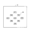
- FIG. 5A illustrates an arrangement of zones of pixels used for focusing and exposure analysis.
- Z 00 through Z 08 illustrate zones within an image sensor 20 that would be used for focus analysis.
- the analysis can be done by allowing the user to select a single one of these zones for AF and/or AE.
- a multi-zone analysis can use data from all of these zones, adaptively weighting each zone based on a variety of criteria, such as local contrast behavior, camera orientation (from sensor 19 or from a user selection), and camera setting information.
- a particular focus zone Z 02 ( 302 ) is shown in an expanded illustration FIG. 5B .
- FIG. 5B shows emphasized panchromatic pixels 302 used for focusing in a sensor with panchromatic and color pixels.
- the second group of pixels includes only panchromatic pixels. Because the second group of pixels read for focusing is usually read out more frequently than the first group of pixels, panchromatic pixels are usually preferred for AF analysis. Because reading the second group of pixels more frequently reduces the potential exposure time available for those pixels, the additional photosensitivity of the panchromatic pixels can be an advantage. In some cases, color pixels are preferred.
- the first group of pixels includes either panchromatic or color pixels or both and the second group of pixels includes either panchromatic or color pixels or both. The key differentiation between pixels in the two groups is function.
- the second video signal is used for adjusting focus, exposure, and other parameters of the capture device.
- the first video signal is used to provide a low resolution or preview image of the overall scene.
- all pixels from the two-dimensional image sensor can be read out, to provide a final capture of an image of the scene after adjustment of capture parameter(s).
- FIG. 5C illustrates how emphasized pixels used for focusing ( 302 ) are distinct from emphasized hatched pixels read out for display purposes ( 350 ). This allows them to have different exposure times and readout rates.
Landscapes
- Engineering & Computer Science (AREA)
- Multimedia (AREA)
- Signal Processing (AREA)
- Studio Devices (AREA)
- Transforming Light Signals Into Electric Signals (AREA)
- Television Systems (AREA)
- Color Television Image Signal Generators (AREA)
Abstract
Description
-
- a) providing a two-dimensional image sensor having a plurality of pixels;
- b) reading a first group of pixels from the image sensor at a first frame rate to produce a first video signal of the image scene;
- c) reading a second group of pixels from the image sensor at a second frame rate to produce a second video signal; and
- d) using at least one of the video signals for adjusting one or more of the capture device parameters.
- 8 focus control
- 9 zoom control
- 10 light from subject scene
- 11 imaging stage
- 12 lens
- 13 filter assembly
- 14 iris
- 16 brightness sensor
- 18 shutter
- 19 orientation sensor
- 20 image sensor
- 22 analog signal processor
- 24 analog to digital (A/D) converter
- 26 timing generator
- 28 image sensor stage
- 30 digital signal processor (DSP) bus
- 32 digital signal processor (DSP) memory
- 36 digital signal processor (DSP)
- 38 processing stage
- 50 system controller
- 52 system controller bus
- 54 program memory
- 56 system memory
- 57 host interface
- 60 memory card interface
- 62 memory card socket
- 64 memory card
- 68 user control and status interface
- 70 viewfinder display
- 72 exposure display
- 74 user inputs
- 76 status display
- 80 video encoder
- 82 display controller
- 88 image display
- 150 prior art time interval
- 152 first group overlapping time interval
- 153 second group overlapping time interval
- 154 non-overlapping
time interval option 1 - 156 non-overlapping
time interval option 2 - 157 non-overlapping
time interval option 3 - 158 non-overlapping
time interval option 4 - 200 user preview block
- 202 user scene mode block
- 205 user actuation block
- 210 initial focus block
- 215 integrate image block
- 220 read second group of pixels block
- 225 contrast calculation block
- 230 focus adjustment block
- 235 focus acceptable decision block
- 240 clear sensor block
- 245 integrate full image block
- 250 read from sensor block
- 302 focus zone
- 350 pixels read out for display purposes
Claims (11)
Priority Applications (5)
| Application Number | Priority Date | Filing Date | Title |
|---|---|---|---|
| US11/538,599 US8031258B2 (en) | 2006-10-04 | 2006-10-04 | Providing multiple video signals from single sensor |
| EP07838755.2A EP2067353B1 (en) | 2006-10-04 | 2007-09-24 | Providing multiple video signals from single sensor |
| JP2009531389A JP5086357B2 (en) | 2006-10-04 | 2007-09-24 | Multiple video signal supply from signal sensor |
| PCT/US2007/020612 WO2008045198A2 (en) | 2006-10-04 | 2007-09-24 | Providing multiple video signals from single sensor |
| US13/220,512 US8416339B2 (en) | 2006-10-04 | 2011-08-29 | Providing multiple video signals from single sensor |
Applications Claiming Priority (1)
| Application Number | Priority Date | Filing Date | Title |
|---|---|---|---|
| US11/538,599 US8031258B2 (en) | 2006-10-04 | 2006-10-04 | Providing multiple video signals from single sensor |
Related Child Applications (1)
| Application Number | Title | Priority Date | Filing Date |
|---|---|---|---|
| US13/220,512 Continuation US8416339B2 (en) | 2006-10-04 | 2011-08-29 | Providing multiple video signals from single sensor |
Publications (2)
| Publication Number | Publication Date |
|---|---|
| US20080084486A1 US20080084486A1 (en) | 2008-04-10 |
| US8031258B2 true US8031258B2 (en) | 2011-10-04 |
Family
ID=39259456
Family Applications (2)
| Application Number | Title | Priority Date | Filing Date |
|---|---|---|---|
| US11/538,599 Active 2029-05-12 US8031258B2 (en) | 2006-10-04 | 2006-10-04 | Providing multiple video signals from single sensor |
| US13/220,512 Active US8416339B2 (en) | 2006-10-04 | 2011-08-29 | Providing multiple video signals from single sensor |
Family Applications After (1)
| Application Number | Title | Priority Date | Filing Date |
|---|---|---|---|
| US13/220,512 Active US8416339B2 (en) | 2006-10-04 | 2011-08-29 | Providing multiple video signals from single sensor |
Country Status (4)
| Country | Link |
|---|---|
| US (2) | US8031258B2 (en) |
| EP (1) | EP2067353B1 (en) |
| JP (1) | JP5086357B2 (en) |
| WO (1) | WO2008045198A2 (en) |
Cited By (16)
| Publication number | Priority date | Publication date | Assignee | Title |
|---|---|---|---|---|
| US20090040344A1 (en) * | 2007-08-06 | 2009-02-12 | Canon Kabushiki Kaisha | Imaging apparatus and control method thereof |
| US20110085062A1 (en) * | 2009-10-13 | 2011-04-14 | Omnivision Technologies, Inc. | System and method for improved image processing |
| US20110310279A1 (en) * | 2006-10-04 | 2011-12-22 | Omnivision Technologies, Inc. | Providing multiple video signals from single sensor |
| US8139130B2 (en) | 2005-07-28 | 2012-03-20 | Omnivision Technologies, Inc. | Image sensor with improved light sensitivity |
| US8194296B2 (en) | 2006-05-22 | 2012-06-05 | Omnivision Technologies, Inc. | Image sensor with improved light sensitivity |
| US8274715B2 (en) | 2005-07-28 | 2012-09-25 | Omnivision Technologies, Inc. | Processing color and panchromatic pixels |
| US20130129146A1 (en) * | 2011-01-18 | 2013-05-23 | Chanan Gabay | Methods, Circuits, Devices, Apparatuses and Systems for Providing Image Composition Rules, Analysis and Improvement |
| US8487996B2 (en) | 2011-04-25 | 2013-07-16 | Skybox Imaging, Inc. | Systems and methods for overhead imaging and video |
| US20180174365A1 (en) * | 2016-12-19 | 2018-06-21 | Intel Corporation | Image stream switcher |
| US10033942B1 (en) * | 2012-05-25 | 2018-07-24 | Altia Systems, Inc. | Real time video system with high dynamic range |
| US10615513B2 (en) | 2015-06-16 | 2020-04-07 | Urthecast Corp | Efficient planar phased array antenna assembly |
| US10871561B2 (en) | 2015-03-25 | 2020-12-22 | Urthecast Corp. | Apparatus and methods for synthetic aperture radar with digital beamforming |
| US10955546B2 (en) | 2015-11-25 | 2021-03-23 | Urthecast Corp. | Synthetic aperture radar imaging apparatus and methods |
| US11378682B2 (en) | 2017-05-23 | 2022-07-05 | Spacealpha Insights Corp. | Synthetic aperture radar imaging apparatus and methods for moving targets |
| US11506778B2 (en) | 2017-05-23 | 2022-11-22 | Spacealpha Insights Corp. | Synthetic aperture radar imaging apparatus and methods |
| US11525910B2 (en) | 2017-11-22 | 2022-12-13 | Spacealpha Insights Corp. | Synthetic aperture radar apparatus and methods |
Families Citing this family (88)
| Publication number | Priority date | Publication date | Assignee | Title |
|---|---|---|---|---|
| JP2008096868A (en) | 2006-10-16 | 2008-04-24 | Sony Corp | Imaging display device, and imaging display method |
| KR100860684B1 (en) * | 2007-01-31 | 2008-09-26 | 삼성전자주식회사 | Display apparatus with display brightness control function |
| JP4951440B2 (en) * | 2007-08-10 | 2012-06-13 | 富士フイルム株式会社 | Imaging apparatus and solid-state imaging device driving method |
| JP4587185B2 (en) * | 2008-02-27 | 2010-11-24 | キヤノン株式会社 | IMAGING SYSTEM AND IMAGING DEVICE CONTROL METHOD |
| US8866920B2 (en) | 2008-05-20 | 2014-10-21 | Pelican Imaging Corporation | Capturing and processing of images using monolithic camera array with heterogeneous imagers |
| US11792538B2 (en) | 2008-05-20 | 2023-10-17 | Adeia Imaging Llc | Capturing and processing of images including occlusions focused on an image sensor by a lens stack array |
| EP3328048B1 (en) | 2008-05-20 | 2021-04-21 | FotoNation Limited | Capturing and processing of images using monolithic camera array with heterogeneous imagers |
| JP5138521B2 (en) * | 2008-09-19 | 2013-02-06 | 富士フイルム株式会社 | Imaging apparatus and imaging method |
| US8224082B2 (en) * | 2009-03-10 | 2012-07-17 | Omnivision Technologies, Inc. | CFA image with synthetic panchromatic image |
| US8179466B2 (en) * | 2009-03-11 | 2012-05-15 | Eastman Kodak Company | Capture of video with motion-speed determination and variable capture rate |
| US8068153B2 (en) * | 2009-03-27 | 2011-11-29 | Omnivision Technologies, Inc. | Producing full-color image using CFA image |
| US8045024B2 (en) * | 2009-04-15 | 2011-10-25 | Omnivision Technologies, Inc. | Producing full-color image with reduced motion blur |
| US8203633B2 (en) * | 2009-05-27 | 2012-06-19 | Omnivision Technologies, Inc. | Four-channel color filter array pattern |
| US8237831B2 (en) * | 2009-05-28 | 2012-08-07 | Omnivision Technologies, Inc. | Four-channel color filter array interpolation |
| US8125546B2 (en) * | 2009-06-05 | 2012-02-28 | Omnivision Technologies, Inc. | Color filter array pattern having four-channels |
| JP5404194B2 (en) * | 2009-06-05 | 2014-01-29 | キヤノン株式会社 | Solid-state imaging device, imaging system, and solid-state imaging device driving method |
| US8253832B2 (en) * | 2009-06-09 | 2012-08-28 | Omnivision Technologies, Inc. | Interpolation for four-channel color filter array |
| EP2502115A4 (en) | 2009-11-20 | 2013-11-06 | Pelican Imaging Corp | Capturing and processing of images using monolithic camera array with heterogeneous imagers |
| SG10201503516VA (en) | 2010-05-12 | 2015-06-29 | Pelican Imaging Corp | Architectures for imager arrays and array cameras |
| WO2012001868A1 (en) * | 2010-07-02 | 2012-01-05 | パナソニック株式会社 | Solid-state image capture element and image capture device comprising said solid-state image capture element, and image capture control method and image capture control program |
| US9118842B2 (en) * | 2010-09-16 | 2015-08-25 | Intellectual Ventures Fund 83 Llc | Producing focused videos from single captured video |
| US20140192238A1 (en) | 2010-10-24 | 2014-07-10 | Linx Computational Imaging Ltd. | System and Method for Imaging and Image Processing |
| US8878950B2 (en) | 2010-12-14 | 2014-11-04 | Pelican Imaging Corporation | Systems and methods for synthesizing high resolution images using super-resolution processes |
| CN103053163A (en) * | 2010-12-16 | 2013-04-17 | 松下电器产业株式会社 | Image generation device, and image generation system, method, and program |
| US8803952B2 (en) * | 2010-12-20 | 2014-08-12 | Microsoft Corporation | Plural detector time-of-flight depth mapping |
| KR101973822B1 (en) | 2011-05-11 | 2019-04-29 | 포토네이션 케이맨 리미티드 | Systems and methods for transmitting and receiving array camera image data |
| KR101760347B1 (en) | 2011-05-17 | 2017-07-24 | 삼성전자주식회사 | Digital photographing apparatus and control method thereof |
| US20130265459A1 (en) | 2011-06-28 | 2013-10-10 | Pelican Imaging Corporation | Optical arrangements for use with an array camera |
| JP2014521117A (en) | 2011-06-28 | 2014-08-25 | ペリカン イメージング コーポレイション | Optical array for use with array cameras |
| JP5862126B2 (en) * | 2011-09-06 | 2016-02-16 | ソニー株式会社 | Imaging device and method, and imaging apparatus |
| WO2013043751A1 (en) | 2011-09-19 | 2013-03-28 | Pelican Imaging Corporation | Systems and methods for controlling aliasing in images captured by an array camera for use in super resolution processing using pixel apertures |
| IN2014CN02708A (en) | 2011-09-28 | 2015-08-07 | Pelican Imaging Corp | |
| WO2013126578A1 (en) | 2012-02-21 | 2013-08-29 | Pelican Imaging Corporation | Systems and methods for the manipulation of captured light field image data |
| US9210392B2 (en) | 2012-05-01 | 2015-12-08 | Pelican Imaging Coporation | Camera modules patterned with pi filter groups |
| WO2014005123A1 (en) | 2012-06-28 | 2014-01-03 | Pelican Imaging Corporation | Systems and methods for detecting defective camera arrays, optic arrays, and sensors |
| US20140002674A1 (en) | 2012-06-30 | 2014-01-02 | Pelican Imaging Corporation | Systems and Methods for Manufacturing Camera Modules Using Active Alignment of Lens Stack Arrays and Sensors |
| WO2014031795A1 (en) | 2012-08-21 | 2014-02-27 | Pelican Imaging Corporation | Systems and methods for parallax detection and correction in images captured using array cameras |
| US20140055632A1 (en) | 2012-08-23 | 2014-02-27 | Pelican Imaging Corporation | Feature based high resolution motion estimation from low resolution images captured using an array source |
| EP2888871A4 (en) * | 2012-08-27 | 2016-05-25 | Nokia Technologies Oy | Method and apparatus for recording video sequences |
| US9214013B2 (en) | 2012-09-14 | 2015-12-15 | Pelican Imaging Corporation | Systems and methods for correcting user identified artifacts in light field images |
| EP2901671A4 (en) | 2012-09-28 | 2016-08-24 | Pelican Imaging Corp | Generating images from light fields utilizing virtual viewpoints |
| WO2014078443A1 (en) | 2012-11-13 | 2014-05-22 | Pelican Imaging Corporation | Systems and methods for array camera focal plane control |
| EP2936794A4 (en) * | 2012-12-18 | 2016-08-10 | Nokia Technologies Oy | Method and apparatus for forming a video sequence |
| US9462164B2 (en) | 2013-02-21 | 2016-10-04 | Pelican Imaging Corporation | Systems and methods for generating compressed light field representation data using captured light fields, array geometry, and parallax information |
| US9374512B2 (en) | 2013-02-24 | 2016-06-21 | Pelican Imaging Corporation | Thin form factor computational array cameras and modular array cameras |
| EP2963917B1 (en) * | 2013-02-27 | 2021-04-14 | Nikon Corporation | Electronic apparatus comprising an image sensor |
| US9638883B1 (en) | 2013-03-04 | 2017-05-02 | Fotonation Cayman Limited | Passive alignment of array camera modules constructed from lens stack arrays and sensors based upon alignment information obtained during manufacture of array camera modules using an active alignment process |
| WO2014138697A1 (en) | 2013-03-08 | 2014-09-12 | Pelican Imaging Corporation | Systems and methods for high dynamic range imaging using array cameras |
| US8866912B2 (en) | 2013-03-10 | 2014-10-21 | Pelican Imaging Corporation | System and methods for calibration of an array camera using a single captured image |
| US9521416B1 (en) | 2013-03-11 | 2016-12-13 | Kip Peli P1 Lp | Systems and methods for image data compression |
| US9519972B2 (en) | 2013-03-13 | 2016-12-13 | Kip Peli P1 Lp | Systems and methods for synthesizing images from image data captured by an array camera using restricted depth of field depth maps in which depth estimation precision varies |
| US9106784B2 (en) | 2013-03-13 | 2015-08-11 | Pelican Imaging Corporation | Systems and methods for controlling aliasing in images captured by an array camera for use in super-resolution processing |
| WO2014164550A2 (en) | 2013-03-13 | 2014-10-09 | Pelican Imaging Corporation | System and methods for calibration of an array camera |
| US9888194B2 (en) | 2013-03-13 | 2018-02-06 | Fotonation Cayman Limited | Array camera architecture implementing quantum film image sensors |
| US9100586B2 (en) | 2013-03-14 | 2015-08-04 | Pelican Imaging Corporation | Systems and methods for photometric normalization in array cameras |
| WO2014159779A1 (en) | 2013-03-14 | 2014-10-02 | Pelican Imaging Corporation | Systems and methods for reducing motion blur in images or video in ultra low light with array cameras |
| US9633442B2 (en) | 2013-03-15 | 2017-04-25 | Fotonation Cayman Limited | Array cameras including an array camera module augmented with a separate camera |
| US9497429B2 (en) | 2013-03-15 | 2016-11-15 | Pelican Imaging Corporation | Extended color processing on pelican array cameras |
| US9497370B2 (en) | 2013-03-15 | 2016-11-15 | Pelican Imaging Corporation | Array camera architecture implementing quantum dot color filters |
| US10122993B2 (en) | 2013-03-15 | 2018-11-06 | Fotonation Limited | Autofocus system for a conventional camera that uses depth information from an array camera |
| US9445003B1 (en) | 2013-03-15 | 2016-09-13 | Pelican Imaging Corporation | Systems and methods for synthesizing high resolution images using image deconvolution based on motion and depth information |
| EP2973476A4 (en) | 2013-03-15 | 2017-01-18 | Pelican Imaging Corporation | Systems and methods for stereo imaging with camera arrays |
| US9584746B2 (en) * | 2013-06-05 | 2017-02-28 | Sony Corporation | Image processing device and imaging method for obtaining a high resolution image and efficient speed for a feedback control signal |
| US9898856B2 (en) | 2013-09-27 | 2018-02-20 | Fotonation Cayman Limited | Systems and methods for depth-assisted perspective distortion correction |
| JP2015111251A (en) * | 2013-11-06 | 2015-06-18 | パナソニックIpマネジメント株式会社 | Imaging device |
| US9185276B2 (en) | 2013-11-07 | 2015-11-10 | Pelican Imaging Corporation | Methods of manufacturing array camera modules incorporating independently aligned lens stacks |
| US10119808B2 (en) | 2013-11-18 | 2018-11-06 | Fotonation Limited | Systems and methods for estimating depth from projected texture using camera arrays |
| WO2015081279A1 (en) | 2013-11-26 | 2015-06-04 | Pelican Imaging Corporation | Array camera configurations incorporating multiple constituent array cameras |
| US9854216B2 (en) * | 2013-12-10 | 2017-12-26 | Canon Kabushiki Kaisha | Image pickup apparatus that displays image based on signal output from image pickup device, method of controlling the same, and storage medium |
| US10089740B2 (en) | 2014-03-07 | 2018-10-02 | Fotonation Limited | System and methods for depth regularization and semiautomatic interactive matting using RGB-D images |
| JP6066949B2 (en) * | 2014-03-14 | 2017-01-25 | キヤノン株式会社 | Imaging apparatus, control method therefor, and program |
| US9247117B2 (en) | 2014-04-07 | 2016-01-26 | Pelican Imaging Corporation | Systems and methods for correcting for warpage of a sensor array in an array camera module by introducing warpage into a focal plane of a lens stack array |
| US9521319B2 (en) | 2014-06-18 | 2016-12-13 | Pelican Imaging Corporation | Array cameras and array camera modules including spectral filters disposed outside of a constituent image sensor |
| JP2017531976A (en) | 2014-09-29 | 2017-10-26 | フォトネイション ケイマン リミテッド | System and method for dynamically calibrating an array camera |
| US9942474B2 (en) | 2015-04-17 | 2018-04-10 | Fotonation Cayman Limited | Systems and methods for performing high speed video capture and depth estimation using array cameras |
| US10440288B2 (en) | 2015-09-02 | 2019-10-08 | Microsoft Technology Licensing, Llc | Methods and apparatuses for capturing image frames with interlaced exposure |
| CN107690648B (en) * | 2016-10-20 | 2022-03-04 | 深圳达闼科技控股有限公司 | Image preview method and device based on iris recognition |
| US10482618B2 (en) | 2017-08-21 | 2019-11-19 | Fotonation Limited | Systems and methods for hybrid depth regularization |
| MX2022003020A (en) | 2019-09-17 | 2022-06-14 | Boston Polarimetrics Inc | Systems and methods for surface modeling using polarization cues. |
| JP7020463B2 (en) * | 2019-09-19 | 2022-02-16 | 株式会社ニコン | Imaging device |
| DE112020004813B4 (en) | 2019-10-07 | 2023-02-09 | Boston Polarimetrics, Inc. | System for expanding sensor systems and imaging systems with polarization |
| CN114787648B (en) | 2019-11-30 | 2023-11-10 | 波士顿偏振测定公司 | Systems and methods for transparent object segmentation using polarization cues |
| US11195303B2 (en) | 2020-01-29 | 2021-12-07 | Boston Polarimetrics, Inc. | Systems and methods for characterizing object pose detection and measurement systems |
| JP2023511747A (en) | 2020-01-30 | 2023-03-22 | イントリンジック イノベーション エルエルシー | Systems and methods for synthesizing data for training statistical models with different imaging modalities, including polarization imaging |
| US11953700B2 (en) | 2020-05-27 | 2024-04-09 | Intrinsic Innovation Llc | Multi-aperture polarization optical systems using beam splitters |
| US11954886B2 (en) | 2021-04-15 | 2024-04-09 | Intrinsic Innovation Llc | Systems and methods for six-degree of freedom pose estimation of deformable objects |
| US11290658B1 (en) | 2021-04-15 | 2022-03-29 | Boston Polarimetrics, Inc. | Systems and methods for camera exposure control |
| US11689813B2 (en) | 2021-07-01 | 2023-06-27 | Intrinsic Innovation Llc | Systems and methods for high dynamic range imaging using crossed polarizers |
Citations (15)
| Publication number | Priority date | Publication date | Assignee | Title |
|---|---|---|---|---|
| US20010055064A1 (en) | 2000-06-02 | 2001-12-27 | Tetsuya Minakami | Digital still camera |
| US6510283B1 (en) * | 1999-11-22 | 2003-01-21 | Canon Kabushiki Kaisha | Photo-taking apparatus, control method adapted for the photo-taking apparatus, and computer program product supplying control program adapted for the photo-taking apparatus |
| US6665449B1 (en) * | 1999-09-03 | 2003-12-16 | Battelle Memorial Institute | Method and algorithm for image processing |
| US20040090550A1 (en) * | 2002-10-26 | 2004-05-13 | Samsung Techwin Co., Ltd. | Image sensing means for digital camera and digital camera adopting the same |
| US6784939B1 (en) * | 1998-10-28 | 2004-08-31 | Hyundai Electronics Industries Co., Ltd. | Apparatus and method for automatically controlling exposure time using a mean value of green pixels |
| US20040212714A1 (en) * | 2003-04-24 | 2004-10-28 | Konica Minolta Opto, Inc. | Digital camera |
| US20050094071A1 (en) * | 2002-03-26 | 2005-05-05 | Masahiko Akiyama | Display device and method of manufacturing the same |
| US20050151729A1 (en) * | 1995-09-20 | 2005-07-14 | Hajime Akimoto | Image display |
| US20050231618A1 (en) * | 2004-03-30 | 2005-10-20 | Toshinobu Sugiyama | Image-capturing apparatus |
| US6972799B1 (en) * | 1997-09-26 | 2005-12-06 | Olympus Optical Co., Ltd. | Auto focusing apparatus selectively operable in an ordinary mode and a high speed mode |
| US20060043189A1 (en) * | 2004-08-31 | 2006-03-02 | Sachin Agrawal | Method and apparatus for determining the vertices of a character in a two-dimensional barcode symbol |
| US20060088298A1 (en) * | 2002-05-08 | 2006-04-27 | Ball Aerospace & Technologies Corp. | One chip camera with color sensing capability and high limiting resolution |
| US20060204122A1 (en) * | 2005-03-08 | 2006-09-14 | Casio Computer Co., Ltd. | Camera with autofocus function |
| JP2007150643A (en) | 2005-11-28 | 2007-06-14 | Sony Corp | Solid state imaging element, driving method therefor, and imaging apparatus |
| US20070210244A1 (en) * | 2006-03-09 | 2007-09-13 | Northrop Grumman Corporation | Spectral filter for optical sensor |
Family Cites Families (289)
| Publication number | Priority date | Publication date | Assignee | Title |
|---|---|---|---|---|
| US2508267A (en) | 1945-10-26 | 1950-05-16 | Du Mont Allen B Lab Inc | Color television |
| US2446791A (en) | 1946-06-11 | 1948-08-10 | Rca Corp | Color television tube |
| US2884483A (en) | 1955-03-09 | 1959-04-28 | Grimson Color Inc | Color image pick up apparatus |
| JPS5016134B1 (en) | 1970-12-26 | 1975-06-11 | ||
| US3971065A (en) | 1975-03-05 | 1976-07-20 | Eastman Kodak Company | Color imaging array |
| JPS6056030B2 (en) | 1975-10-24 | 1985-12-07 | 松下電器産業株式会社 | Color solid-state imaging device |
| US4047203A (en) | 1976-05-12 | 1977-09-06 | Eastman Kodak Company | Color imaging array |
| US4437112A (en) | 1980-02-15 | 1984-03-13 | Canon Kabushiki Kaisha | Solid-state color imaging apparatus |
| JPS5763983A (en) | 1980-10-07 | 1982-04-17 | Toshiba Corp | Color image pickup device |
| US4500914A (en) | 1981-08-01 | 1985-02-19 | Sharp Kabushiki Kaisha | Color imaging array and color imaging device |
| US4591900A (en) | 1983-03-14 | 1986-05-27 | Rca Corporation | Encoding pattern for single chip CCD camera processing scheme |
| EP0119862B1 (en) | 1983-03-17 | 1990-12-27 | Nec Corporation | Solid-state color imaging apparatus |
| JPS6020111A (en) | 1983-07-14 | 1985-02-01 | Fuji Electric Corp Res & Dev Ltd | Distance measuring device |
| US4638352A (en) | 1983-09-16 | 1987-01-20 | Hitachi, Ltd. | Color video camera signal processing circuit |
| JPS60103790A (en) | 1983-11-10 | 1985-06-08 | Nec Corp | Color solid-state image pickup device |
| JPS60226282A (en) | 1984-04-24 | 1985-11-11 | Canon Inc | Image pickup device |
| DE3515020A1 (en) | 1984-04-28 | 1985-11-07 | Kabushiki Kaisha Toshiba, Kawasaki, Kanagawa | LOCAL FREQUENCY FILTER |
| US4642678A (en) | 1984-09-10 | 1987-02-10 | Eastman Kodak Company | Signal processing method and apparatus for producing interpolated chrominance values in a sampled color image signal |
| US4663661A (en) | 1985-05-23 | 1987-05-05 | Eastman Kodak Company | Single sensor color video camera with blurring filter |
| US5018006A (en) | 1985-10-31 | 1991-05-21 | Canon Kabushiki Kaisha | Multi-plate type image pickup apparatus having picture elements for producing color and luminance signals |
| JPS62258563A (en) | 1986-05-01 | 1987-11-11 | Omron Tateisi Electronics Co | Still image pickup camera |
| JP2849813B2 (en) | 1986-12-19 | 1999-01-27 | 富士写真フイルム株式会社 | Video signal forming device |
| US4896207A (en) | 1988-06-17 | 1990-01-23 | Eastman Kodak Company | Color imaging apparatus employing a horizontal stripe color filter to reduce rise-time artifacts |
| DE3824639C2 (en) | 1988-07-20 | 1993-11-18 | Geutebrueck Videotechnik Gmbh | Optical monitoring device |
| US4962419A (en) | 1989-02-13 | 1990-10-09 | Eastman Kodak Company | Detail processing method and apparatus providing uniform processing of horizontal and vertical detail components |
| US5264924A (en) | 1989-12-18 | 1993-11-23 | Eastman Kodak Company | Mechanism for deriving noise-reduced estimates of color signal parameters from multiple color/luminance image sensor outputs |
| EP0446018B1 (en) | 1990-03-05 | 1998-08-12 | Canon Kabushiki Kaisha | Image processing apparatus |
| US5323233A (en) | 1990-07-31 | 1994-06-21 | Canon Kabushiki Kaisha | Image signal processing apparatus having a color filter with offset luminance filter elements |
| US5432906A (en) | 1990-09-28 | 1995-07-11 | Eastman Kodak Company | Color image processing system for preparing a composite image transformation module for performing a plurality of selected image transformations |
| US5272518A (en) | 1990-12-17 | 1993-12-21 | Hewlett-Packard Company | Colorimeter and calibration system |
| EP0528433B1 (en) | 1991-08-21 | 2002-03-06 | Canon Kabushiki Kaisha | Video camera provided with a plurality of photographing modes |
| US5831676A (en) | 1992-08-19 | 1998-11-03 | Canon Kabushiki Kaisha | Image pickup device using plural control parameters for exposure control |
| US5374956A (en) | 1992-05-29 | 1994-12-20 | Eastman Kodak Company | Electronic imaging apparatus with dithered color filter array |
| US5903388A (en) | 1992-06-11 | 1999-05-11 | Sedlmayr Steven R | High efficiency electromagnetic beam projector and systems and method for implementation thereof |
| US5227313A (en) | 1992-07-24 | 1993-07-13 | Eastman Kodak Company | Process for making backside illuminated image sensors |
| US5244817A (en) | 1992-08-03 | 1993-09-14 | Eastman Kodak Company | Method of making backside illuminated image sensors |
| US5382976A (en) | 1993-06-30 | 1995-01-17 | Eastman Kodak Company | Apparatus and method for adaptively interpolating a full color image utilizing luminance gradients |
| US5493335A (en) | 1993-06-30 | 1996-02-20 | Eastman Kodak Company | Single sensor color camera with user selectable image record size |
| US5373322A (en) | 1993-06-30 | 1994-12-13 | Eastman Kodak Company | Apparatus and method for adaptively interpolating a full color image utilizing chrominance gradients |
| JPH0823542A (en) | 1994-07-11 | 1996-01-23 | Canon Inc | Image pickup device |
| DE69514874T2 (en) | 1994-08-23 | 2000-07-20 | Hewlett Packard Co | Sensor arrangement for an optical image scanner which supplies gray value and color signals |
| US6292212B1 (en) | 1994-12-23 | 2001-09-18 | Eastman Kodak Company | Electronic color infrared camera |
| JP3392564B2 (en) | 1995-02-27 | 2003-03-31 | 三洋電機株式会社 | Single-panel color video camera |
| US5670817A (en) | 1995-03-03 | 1997-09-23 | Santa Barbara Research Center | Monolithic-hybrid radiation detector/readout |
| US5629734A (en) | 1995-03-17 | 1997-05-13 | Eastman Kodak Company | Adaptive color plan interpolation in single sensor color electronic camera |
| US5506619A (en) | 1995-03-17 | 1996-04-09 | Eastman Kodak Company | Adaptive color plan interpolation in single sensor color electronic camera |
| US5625210A (en) | 1995-04-13 | 1997-04-29 | Eastman Kodak Company | Active pixel sensor integrated with a pinned photodiode |
| US5677202A (en) | 1995-11-20 | 1997-10-14 | Eastman Kodak Company | Method for making planar color filter array for image sensors with embedded color filter arrays |
| US5596367A (en) | 1996-02-23 | 1997-01-21 | Eastman Kodak Company | Averaging green values for green photosites in electronic cameras |
| US5652621A (en) | 1996-02-23 | 1997-07-29 | Eastman Kodak Company | Adaptive color plane interpolation in single sensor color electronic camera |
| US5786236A (en) | 1996-03-29 | 1998-07-28 | Eastman Kodak Company | Backside thinning using ion-beam figuring |
| JP3752510B2 (en) | 1996-04-15 | 2006-03-08 | イーストマン コダック カンパニー | Automatic subject detection method for images |
| US5631703A (en) | 1996-05-29 | 1997-05-20 | Eastman Kodak Company | Particular pattern of pixels for a color filter array which is used to derive luminance and chrominance values |
| FR2755815B1 (en) | 1996-11-08 | 1998-12-18 | Commissariat Energie Atomique | DEVICE AND METHOD FOR DETERMINING THE PRESUMED POSITION OF AN EVENT IN RELATION TO A SET OF PHOTODETECTORS, AND APPLICATION TO GAMMA-CAMERAS |
| US6246865B1 (en) | 1997-02-04 | 2001-06-12 | Samsung Electronics Co., Ltd. | Device and method for controlling distortion characteristic of predistorter |
| US6243133B1 (en) | 1997-03-07 | 2001-06-05 | Eastman Kodak Company | Method for automatic scene balance of digital images |
| US6115066A (en) | 1997-06-12 | 2000-09-05 | International Business Machines Corporation | Image sensor with direct digital correlated sampling |
| US6366319B1 (en) | 1997-07-03 | 2002-04-02 | Photronics Corp. | Subtractive color processing system for digital imaging |
| JPH1126741A (en) | 1997-07-04 | 1999-01-29 | Toshiba Corp | Solid-state image pick-up device |
| US6097835A (en) | 1997-07-23 | 2000-08-01 | Lockheed Martin Corporation | Projective pan sharpening methods and apparatus |
| US6107655A (en) | 1997-08-15 | 2000-08-22 | Eastman Kodak Company | Active pixel image sensor with shared amplifier read-out |
| US6369853B1 (en) | 1997-11-13 | 2002-04-09 | Foveon, Inc. | Intra-pixel frame storage element, array, and electronic shutter method suitable for electronic still camera applications |
| JP3873157B2 (en) | 1997-11-13 | 2007-01-24 | カシオ計算機株式会社 | Electronic camera device and imaging method |
| JP4006075B2 (en) | 1998-01-30 | 2007-11-14 | キヤノン株式会社 | CMOS sensor and imaging system |
| JP4140077B2 (en) | 1998-02-18 | 2008-08-27 | ソニー株式会社 | Solid-state image sensor driving method, solid-state image sensor, and camera |
| US6366318B1 (en) | 1998-03-27 | 2002-04-02 | Eastman Kodak Company | CFA correction for CFA images captured at partial resolution |
| US5914749A (en) | 1998-03-31 | 1999-06-22 | Intel Corporation | Magenta-white-yellow (MWY) color system for digital image sensor applications |
| US6011875A (en) | 1998-04-29 | 2000-01-04 | Eastman Kodak Company | Process for enhancing the spatial resolution of multispectral imagery using pan-sharpening |
| US6977684B1 (en) | 1998-04-30 | 2005-12-20 | Canon Kabushiki Kaisha | Arrangement of circuits in pixels, each circuit shared by a plurality of pixels, in image sensing apparatus |
| US6040570A (en) | 1998-05-29 | 2000-03-21 | Sarnoff Corporation | Extended dynamic range image sensor system |
| US6529239B1 (en) | 1998-06-01 | 2003-03-04 | Fairchild Imaging, Inc. | Image sensor with stripes of cyan filter material perpendicular to stripes of yellow filter material |
| JP3592147B2 (en) | 1998-08-20 | 2004-11-24 | キヤノン株式会社 | Solid-state imaging device |
| US6734906B1 (en) | 1998-09-02 | 2004-05-11 | Canon Kabushiki Kaisha | Image pickup apparatus with photoelectric conversion portions arranged two dimensionally |
| JP2000152072A (en) | 1998-11-11 | 2000-05-30 | Minolta Co Ltd | Digital camera |
| US6153446A (en) | 1998-11-13 | 2000-11-28 | United Microelectronics Corp. | Method for forming a metallic reflecting layer in a semiconductor photodiode |
| US6429036B1 (en) | 1999-01-14 | 2002-08-06 | Micron Technology, Inc. | Backside illumination of CMOS image sensor |
| JP3784602B2 (en) | 1999-03-08 | 2006-06-14 | シャープ株式会社 | Image reading method and image reading system |
| US6714243B1 (en) | 1999-03-22 | 2004-03-30 | Biomorphic Vlsi, Inc. | Color filter pattern |
| US6947089B1 (en) | 1999-05-14 | 2005-09-20 | Canon Kabushiki Kaisha | Image pickup apparatus |
| US6727521B2 (en) | 2000-09-25 | 2004-04-27 | Foveon, Inc. | Vertical color filter detector group and array |
| EP1208150A4 (en) | 1999-06-11 | 2005-01-26 | Sydney Hyman | Image making medium |
| JP4626007B2 (en) | 1999-06-14 | 2011-02-02 | 株式会社ニコン | Image processing method, machine-readable recording medium storing image processing program, and image processing apparatus |
| JP4077120B2 (en) | 1999-07-01 | 2008-04-16 | 富士フイルム株式会社 | Solid-state imaging device and signal processing method |
| US6168965B1 (en) | 1999-08-12 | 2001-01-02 | Tower Semiconductor Ltd. | Method for making backside illuminated image sensor |
| US6642962B1 (en) | 1999-09-01 | 2003-11-04 | Neomagic Corp. | Merged pipeline for color interpolation and edge enhancement of digital images |
| US6512838B1 (en) | 1999-09-22 | 2003-01-28 | Canesta, Inc. | Methods for enhancing performance and data acquired from three-dimensional image systems |
| US6694064B1 (en) | 1999-11-19 | 2004-02-17 | Positive Systems, Inc. | Digital aerial image mosaic method and apparatus |
| JP3467013B2 (en) | 1999-12-06 | 2003-11-17 | キヤノン株式会社 | Solid-state imaging device |
| US7330209B2 (en) | 1999-12-20 | 2008-02-12 | Texas Instruments Incorporated | Digital still camera system and complementary-color-filtered array interpolation method |
| US6221687B1 (en) | 1999-12-23 | 2001-04-24 | Tower Semiconductor Ltd. | Color image sensor with embedded microlens array |
| JP4368513B2 (en) | 1999-12-27 | 2009-11-18 | 富士フイルム株式会社 | Image processing method and apparatus, and recording medium |
| US6757012B1 (en) | 2000-01-13 | 2004-06-29 | Biomorphic Vlsi, Inc. | Color selection for sparse color image reconstruction |
| JP4195169B2 (en) | 2000-03-14 | 2008-12-10 | 富士フイルム株式会社 | Solid-state imaging device and signal processing method |
| US20010054723A1 (en) | 2000-03-17 | 2001-12-27 | Tadashi Narui | Image sensor, method of fabricating the same, and exposure apparatus, measuring device, alignment device, and aberration measuring device using the image sensor |
| US6453124B2 (en) | 2000-03-27 | 2002-09-17 | Minolta Co., Ltd. | Digital camera |
| US6876384B1 (en) | 2000-04-19 | 2005-04-05 | Biomorphic Vlsi, Inc. | Pixel selective white balancing |
| US6960817B2 (en) | 2000-04-21 | 2005-11-01 | Canon Kabushiki Kaisha | Solid-state imaging device |
| US6515275B1 (en) | 2000-04-24 | 2003-02-04 | Hewlett-Packard Company | Method and apparatus for determining the illumination type in a scene |
| US6441855B1 (en) | 2000-05-09 | 2002-08-27 | Eastman Kodak Company | Focusing device |
| US6441848B1 (en) | 2000-05-19 | 2002-08-27 | Damon L. Tull | Preventing blur caused by motion of the subject in a digital image |
| US6594388B1 (en) | 2000-05-25 | 2003-07-15 | Eastman Kodak Company | Color image reproduction of scenes with preferential color mapping and scene-dependent tone scaling |
| JP3745948B2 (en) | 2000-08-25 | 2006-02-15 | シャープ株式会社 | Image processing apparatus and digital camera |
| US6995795B1 (en) | 2000-09-12 | 2006-02-07 | Eastman Kodak Company | Method for reducing dark current |
| JP4517493B2 (en) | 2000-10-18 | 2010-08-04 | ソニー株式会社 | Solid-state imaging device and signal processing method thereof |
| DE60144528D1 (en) | 2000-10-19 | 2011-06-09 | Quantum Semiconductor Llc | METHOD FOR PRODUCING CMOS INTEGRATED HETEROVER PHOTODODMS |
| US6937774B1 (en) | 2000-10-24 | 2005-08-30 | Lockheed Martin Corporation | Apparatus and method for efficiently increasing the spatial resolution of images |
| US6813046B1 (en) | 2000-11-07 | 2004-11-02 | Eastman Kodak Company | Method and apparatus for exposure control for a sparsely sampled extended dynamic range image sensing device |
| US6765611B1 (en) | 2000-11-21 | 2004-07-20 | Eastman Kodak Company | Method for compressing an image from a sparsely sampled extended dynamic range image sensing device |
| US6646246B1 (en) | 2000-11-21 | 2003-11-11 | Eastman Kodak Company | Method and system of noise removal for a sparsely sampled extended dynamic range image sensing device |
| US6943831B2 (en) | 2001-01-24 | 2005-09-13 | Eastman Kodak Company | Method and apparatus to extend the effective dynamic range of an image sensing device and use residual images |
| US6889620B2 (en) | 2001-02-28 | 2005-05-10 | The Mosaic Company | Method for prescribing site-specific fertilizer application in agricultural fields |
| US6476865B1 (en) | 2001-03-07 | 2002-11-05 | Eastman Kodak Company | Sparsely sampled image sensing device with color and luminance photosites |
| JP4139088B2 (en) | 2001-03-08 | 2008-08-27 | 富士フイルム株式会社 | Solid-state imaging device and control method thereof |
| US8120690B2 (en) | 2001-04-12 | 2012-02-21 | Nikon Corporation | Imaging device |
| WO2002090887A2 (en) | 2001-05-04 | 2002-11-14 | Vexcel Imaging Gmbh | Digital camera for and method of obtaining overlapping images |
| KR100436067B1 (en) | 2001-11-16 | 2004-06-12 | 주식회사 하이닉스반도체 | Image sensor and method of fabricating the same |
| US6611380B2 (en) | 2001-12-21 | 2003-08-26 | Eastman Kodak Company | System and method for calibration of display system with linear array modulator |
| JP3992992B2 (en) | 2002-02-19 | 2007-10-17 | 株式会社リコー | Subject image acquisition device |
| JP4198449B2 (en) | 2002-02-22 | 2008-12-17 | 富士フイルム株式会社 | Digital camera |
| JP2003299112A (en) | 2002-03-29 | 2003-10-17 | Fuji Photo Film Co Ltd | Digital camera |
| JP2004023747A (en) * | 2002-06-20 | 2004-01-22 | Minolta Co Ltd | Electronic camera |
| WO2004001667A2 (en) | 2002-06-21 | 2003-12-31 | The Trustees Of Columbia University In The City Of New York | Systems and methods for de-blurring motion blurred images |
| US7015961B2 (en) | 2002-08-16 | 2006-03-21 | Ramakrishna Kakarala | Digital image system and method for combining demosaicing and bad pixel correction |
| WO2004027879A2 (en) | 2002-09-19 | 2004-04-01 | Quantum Semiconductor Llc | Light-sensing device |
| US7206072B2 (en) | 2002-10-04 | 2007-04-17 | Fujifilm Corporation | Light source type discriminating method, image forming method, method and apparatus for estimating light source energy distribution, and exposure amount determining method |
| US7084906B2 (en) | 2002-10-15 | 2006-08-01 | Eastman Kodak Company | Reducing computation time in removing color aliasing artifacts from color digital images |
| JP2004147093A (en) | 2002-10-24 | 2004-05-20 | Canon Inc | Apparatus and method for signal processing, and imaging apparatus |
| US7400770B2 (en) | 2002-11-06 | 2008-07-15 | Hrl Laboratories | Method and apparatus for automatically extracting geospatial features from multispectral imagery suitable for fast and robust extraction of landmarks |
| CN100405598C (en) | 2002-11-12 | 2008-07-23 | 微米技术有限公司 | Grounded gate and isolation techniques for reducing dark current in CMOS image sensors |
| US7091536B2 (en) | 2002-11-14 | 2006-08-15 | Micron Technology, Inc. | Isolation process and structure for CMOS imagers |
| US7327504B2 (en) | 2002-12-06 | 2008-02-05 | Eastman Kodak Company | Method of detecting clipped image pixels |
| WO2004054001A2 (en) | 2002-12-09 | 2004-06-24 | Quantum Semiconductor Llc | Cmos image sensor |
| US7453129B2 (en) | 2002-12-18 | 2008-11-18 | Noble Peak Vision Corp. | Image sensor comprising isolated germanium photodetectors integrated with a silicon substrate and silicon circuitry |
| US20060055800A1 (en) | 2002-12-18 | 2006-03-16 | Noble Device Technologies Corp. | Adaptive solid state image sensor |
| JP4019417B2 (en) | 2003-01-14 | 2007-12-12 | ソニー株式会社 | Image processing apparatus and method, recording medium, and program |
| US7340099B2 (en) | 2003-01-17 | 2008-03-04 | University Of New Brunswick | System and method for image fusion |
| JP3804617B2 (en) | 2003-02-14 | 2006-08-02 | コニカミノルタフォトイメージング株式会社 | Image processing apparatus and method |
| US20040174446A1 (en) | 2003-02-28 | 2004-09-09 | Tinku Acharya | Four-color mosaic pattern for depth and image capture |
| JP2004304706A (en) | 2003-04-01 | 2004-10-28 | Fuji Photo Film Co Ltd | Solid-state imaging apparatus and interpolation processing method thereof |
| JP3877695B2 (en) | 2003-04-03 | 2007-02-07 | 松下電器産業株式会社 | Color solid-state imaging device |
| FI20030583A (en) | 2003-04-16 | 2004-10-17 | Upstream Engineering Oy | Beamer |
| JP4120453B2 (en) | 2003-04-18 | 2008-07-16 | ソニー株式会社 | Solid-state imaging device and drive control method thereof |
| JP2004341206A (en) | 2003-05-15 | 2004-12-02 | Olympus Corp | Display apparatus |
| US7462553B2 (en) | 2003-06-25 | 2008-12-09 | Semicoa | Ultra thin back-illuminated photodiode array fabrication methods |
| US8264576B2 (en) | 2007-03-05 | 2012-09-11 | DigitalOptics Corporation Europe Limited | RGBW sensor array |
| US6984816B2 (en) | 2003-08-13 | 2006-01-10 | Motorola, Inc. | Vertically integrated photosensor for CMOS imagers |
| US6927432B2 (en) | 2003-08-13 | 2005-08-09 | Motorola, Inc. | Vertically integrated photosensor for CMOS imagers |
| US6809008B1 (en) | 2003-08-28 | 2004-10-26 | Motorola, Inc. | Integrated photosensor for CMOS imagers |
| JP4349048B2 (en) | 2003-09-22 | 2009-10-21 | セイコーエプソン株式会社 | projector |
| CN1879397A (en) | 2003-10-13 | 2006-12-13 | 卓越设备技术公司 | Image sensor comprising isolated germanium photodetectors integrated with a silicon substrate and silicon circuitry |
| US7214999B2 (en) | 2003-10-31 | 2007-05-08 | Motorola, Inc. | Integrated photoserver for CMOS imagers |
| JP4075773B2 (en) | 2003-11-05 | 2008-04-16 | ソニー株式会社 | Solid-state imaging device |
| JP4046069B2 (en) | 2003-11-17 | 2008-02-13 | ソニー株式会社 | Solid-state imaging device and manufacturing method of solid-state imaging device |
| US7379588B2 (en) | 2003-11-25 | 2008-05-27 | Xerox Corporation | Systems for spectral multiplexing of source images to provide a composite image, for rendering the composite image, and for spectral demultiplexing the composite image to obtain a normalized color image |
| JP4412710B2 (en) | 2003-11-25 | 2010-02-10 | キヤノン株式会社 | Method for designing photoelectric conversion device |
| US7528997B2 (en) | 2003-12-22 | 2009-05-05 | Xerox Corporation | Systems and methods for streak detection in image array scanning |
| KR100595898B1 (en) | 2003-12-31 | 2006-07-03 | 동부일렉트로닉스 주식회사 | Image sensor and method for fabricating the same |
| US7075129B2 (en) | 2004-01-09 | 2006-07-11 | Eastman Kodak Company | Image sensor with reduced p-well conductivity |
| JP2005268738A (en) | 2004-02-17 | 2005-09-29 | Sony Corp | Solid-state imaging device and its manufacturing method, and semiconductor integrated circuit device and its manufacturing method |
| JP4426885B2 (en) * | 2004-03-23 | 2010-03-03 | オリンパス株式会社 | Solid-state imaging device |
| EP1594321A3 (en) | 2004-05-07 | 2006-01-25 | Dialog Semiconductor GmbH | Extended dynamic range in color imagers |
| JP2005333265A (en) * | 2004-05-18 | 2005-12-02 | Olympus Corp | Solid state imaging element and unit |
| JP2005354610A (en) | 2004-06-14 | 2005-12-22 | Canon Inc | Image processing apparatus, image processing method and image processing program |
| JP4211696B2 (en) | 2004-06-30 | 2009-01-21 | ソニー株式会社 | Method for manufacturing solid-state imaging device |
| US7298922B1 (en) | 2004-07-07 | 2007-11-20 | Lockheed Martin Corporation | Synthetic panchromatic imagery method and system |
| US7652703B2 (en) | 2004-07-12 | 2010-01-26 | Micron Technology, Inc. | Dual panel pixel readout in an imager |
| US7880785B2 (en) | 2004-07-21 | 2011-02-01 | Aptina Imaging Corporation | Rod and cone response sensor |
| US8570389B2 (en) | 2004-07-22 | 2013-10-29 | Broadcom Corporation | Enhancing digital photography |
| US7385238B2 (en) | 2004-08-16 | 2008-06-10 | Micron Technology, Inc. | Low dark current image sensors with epitaxial SiC and/or carbonated channels for array transistors |
| US7477304B2 (en) | 2004-08-26 | 2009-01-13 | Micron Technology, Inc. | Two narrow band and one wide band color filter for increasing color image sensor sensitivity |
| JP4424120B2 (en) | 2004-08-31 | 2010-03-03 | ソニー株式会社 | Solid-state imaging device and method for manufacturing solid-state imaging device |
| JP4756839B2 (en) | 2004-09-01 | 2011-08-24 | キヤノン株式会社 | Solid-state imaging device and camera |
| JP4916101B2 (en) | 2004-09-01 | 2012-04-11 | キヤノン株式会社 | Photoelectric conversion device, solid-state imaging device, and solid-state imaging system |
| JP2006073736A (en) | 2004-09-01 | 2006-03-16 | Canon Inc | Photoelectric converter, solid state imaging device and system |
| JP4157083B2 (en) | 2004-09-09 | 2008-09-24 | マイクロン テクノロジー,インコーポレイテッド | Image sensor with on-chip half-parallel pipelined analog-to-digital converter |
| US7425460B2 (en) | 2004-09-17 | 2008-09-16 | California Institute Of Technology | Method for implementation of back-illuminated CMOS or CCD imagers |
| US7791663B2 (en) | 2004-10-15 | 2010-09-07 | Omnivision Technologies, Inc. | Image sensor and pixel that has positive transfer gate voltage during integration period |
| US7454053B2 (en) | 2004-10-29 | 2008-11-18 | Mitutoyo Corporation | System and method for automatically recovering video tools in a vision system |
| JP4652773B2 (en) | 2004-11-05 | 2011-03-16 | パナソニック株式会社 | Amplification type solid-state imaging device |
| US7109051B2 (en) | 2004-11-15 | 2006-09-19 | Freescale Semiconductor, Inc. | Method of integrating optical devices and electronic devices on an integrated circuit |
| EP1821128B1 (en) | 2004-11-16 | 2011-03-16 | Citizen Holdings Co., Ltd. | Automatic focusing apparatus |
| EP1659776A1 (en) | 2004-11-23 | 2006-05-24 | Dialog Semiconductor GmbH | An image sensor having resolution adjustment employing an analog column averaging/row averaging for high intensity light or row binning for low intensity light |
| JP2006154354A (en) | 2004-11-30 | 2006-06-15 | Seiko Epson Corp | Forming method of color filter |
| JP2006165975A (en) | 2004-12-07 | 2006-06-22 | Konica Minolta Photo Imaging Inc | Image pickup element, image pickup device and image processing method |
| JP4536072B2 (en) | 2004-12-16 | 2010-09-01 | 富士通セミコンダクター株式会社 | Imaging device |
| KR100699831B1 (en) | 2004-12-16 | 2007-03-27 | 삼성전자주식회사 | Method and apparatus for interpolating Bayer-pattern color signals |
| JP4841834B2 (en) | 2004-12-24 | 2011-12-21 | 浜松ホトニクス株式会社 | Photodiode array |
| JP2006184567A (en) | 2004-12-27 | 2006-07-13 | Toshiba Corp | Projection image display apparatus and brightness adjustment method therefor |
| US7800145B2 (en) | 2004-12-30 | 2010-09-21 | Ess Technology, Inc. | Method and apparatus for controlling charge transfer in CMOS sensors with a transfer gate work function |
| US7635880B2 (en) | 2004-12-30 | 2009-12-22 | Ess Technology, Inc. | Method and apparatus for proximate CMOS pixels |
| EP1679907A1 (en) | 2005-01-05 | 2006-07-12 | Dialog Semiconductor GmbH | Hexagonal color pixel structure with white pixels |
| US7554588B2 (en) | 2005-02-01 | 2009-06-30 | TransChip Israel, Ltd. | Dual exposure for image sensor |
| US7723215B2 (en) | 2005-02-11 | 2010-05-25 | Sarnoff Corporation | Dark current reduction in back-illuminated imaging sensors and method of fabricating same |
| US7238583B2 (en) | 2005-02-11 | 2007-07-03 | Sarnoff Corporation | Back-illuminated imaging device and method of fabricating same |
| US8654201B2 (en) | 2005-02-23 | 2014-02-18 | Hewlett-Packard Development Company, L.P. | Method for deblurring an image |
| EP1701536A1 (en) | 2005-03-08 | 2006-09-13 | Sony Ericsson Mobile Communications AB | Method and device for creating pictures, using global shutter and multiple exposures |
| IL174531A0 (en) | 2005-04-06 | 2006-08-20 | Given Imaging Ltd | System and method for performing capsule endoscopy diagnosis in remote sites |
| US7705900B2 (en) | 2005-06-01 | 2010-04-27 | Eastman Kodak Company | CMOS image sensor pixel with selectable binning and conversion gain |
| KR100672687B1 (en) | 2005-06-03 | 2007-01-22 | 동부일렉트로닉스 주식회사 | CMOS Image sensor and Method for fabricating of the same |
| KR100660865B1 (en) | 2005-06-08 | 2006-12-26 | 삼성전자주식회사 | Pixel circuit having shared interconnections/transistors in image sensor and driving method thereof |
| US20070002153A1 (en) | 2005-06-29 | 2007-01-04 | Bart Dierickx | Hue preservation |
| US8306362B2 (en) | 2005-07-20 | 2012-11-06 | Omnivision Technologies, Inc. | Selective pixel binning and averaging based on scene illuminant |
| US8139130B2 (en) | 2005-07-28 | 2012-03-20 | Omnivision Technologies, Inc. | Image sensor with improved light sensitivity |
| US8274715B2 (en) | 2005-07-28 | 2012-09-25 | Omnivision Technologies, Inc. | Processing color and panchromatic pixels |
| US7830430B2 (en) | 2005-07-28 | 2010-11-09 | Eastman Kodak Company | Interpolation of panchromatic and color pixels |
| US8430809B2 (en) | 2005-08-01 | 2013-04-30 | G. I View Ltd. | Capsule for use in small intestine |
| US20070040922A1 (en) | 2005-08-22 | 2007-02-22 | Micron Technology, Inc. | HDR/AB on multi-way shared pixels |
| US20070046807A1 (en) | 2005-08-23 | 2007-03-01 | Eastman Kodak Company | Capturing images under varying lighting conditions |
| US7315014B2 (en) | 2005-08-30 | 2008-01-01 | Micron Technology, Inc. | Image sensors with optical trench |
| US7829832B2 (en) | 2005-08-30 | 2010-11-09 | Aptina Imaging Corporation | Method for operating a pixel cell using multiple pulses to a transistor transfer gate |
| US20070052050A1 (en) | 2005-09-07 | 2007-03-08 | Bart Dierickx | Backside thinned image sensor with integrated lens stack |
| JP2007086596A (en) | 2005-09-26 | 2007-04-05 | Pentax Corp | Camera |
| KR100710210B1 (en) | 2005-09-28 | 2007-04-20 | 동부일렉트로닉스 주식회사 | CMOS image sensor and method for fabricating the same |
| JP2007095917A (en) | 2005-09-28 | 2007-04-12 | Matsushita Electric Ind Co Ltd | Solid-state imaging device |
| KR100775058B1 (en) | 2005-09-29 | 2007-11-08 | 삼성전자주식회사 | Pixel Cell, Image Sensor Adopting The Pixel Cell, and Image Processing System Including The Image Sensor |
| US7978240B2 (en) | 2005-10-03 | 2011-07-12 | Konica Minolta Photo Imaging, Inc. | Enhancing image quality imaging unit and image sensor |
| JP4622790B2 (en) | 2005-10-03 | 2011-02-02 | コニカミノルタホールディングス株式会社 | Imaging device and imaging apparatus |
| JP5118047B2 (en) | 2005-10-13 | 2013-01-16 | アール・ジェイ・エス・テクノロジー・インコーポレイテッド | System and method for high performance color filter mosaic array |
| WO2007051147A2 (en) | 2005-10-26 | 2007-05-03 | Capso Vision, Inc. | Onboard data storage and method |
| US7812301B2 (en) | 2005-10-28 | 2010-10-12 | Sony Corporation | Solid-state imaging device, method of driving solid-state imaging device and imaging apparatus |
| US7576404B2 (en) | 2005-12-16 | 2009-08-18 | Icemos Technology Ltd. | Backlit photodiode and method of manufacturing a backlit photodiode |
| JP2007180761A (en) | 2005-12-27 | 2007-07-12 | Sanyo Electric Co Ltd | Method for driving solid imaging element, and imaging apparatus |
| US7821553B2 (en) | 2005-12-30 | 2010-10-26 | International Business Machines Corporation | Pixel array, imaging sensor including the pixel array and digital camera including the imaging sensor |
| US20070154202A1 (en) | 2006-01-04 | 2007-07-05 | Lee King F | Method and apparatus to facilitate correcting rolling shutter images |
| US7675080B2 (en) | 2006-01-10 | 2010-03-09 | Aptina Imaging Corp. | Uniform color filter arrays in a moat |
| US20070159542A1 (en) | 2006-01-12 | 2007-07-12 | Gang Luo | Color filter array with neutral elements and color image formation |
| US7688368B2 (en) | 2006-01-27 | 2010-03-30 | Eastman Kodak Company | Image sensor with improved light sensitivity |
| US7586139B2 (en) | 2006-02-17 | 2009-09-08 | International Business Machines Corporation | Photo-sensor and pixel array with backside illumination and method of forming the photo-sensor |
| US7680354B2 (en) | 2006-03-22 | 2010-03-16 | Arcsoft, Inc. | Image deblur based on two images |
| JP5000914B2 (en) | 2006-03-30 | 2012-08-15 | 日東光学株式会社 | Video projection device |
| JP4449936B2 (en) | 2006-03-31 | 2010-04-14 | ソニー株式会社 | Imaging apparatus, camera system, and driving method thereof |
| KR100785528B1 (en) | 2006-05-01 | 2007-12-13 | (주) 픽셀플러스 | Wide dynamic range image sensor and pixel array of image sensor |
| JP5011814B2 (en) | 2006-05-15 | 2012-08-29 | ソニー株式会社 | Imaging apparatus, image processing method, and computer program |
| US7916362B2 (en) | 2006-05-22 | 2011-03-29 | Eastman Kodak Company | Image sensor with improved light sensitivity |
| JP4908067B2 (en) | 2006-06-01 | 2012-04-04 | オリンパス株式会社 | Solid-state imaging device and imaging device system using the same |
| US7706022B2 (en) | 2006-06-12 | 2010-04-27 | Kabushiki Kaisha Toshiba | Image forming apparatus and image forming method |
| JP5106870B2 (en) | 2006-06-14 | 2012-12-26 | 株式会社東芝 | Solid-state image sensor |
| US7561789B2 (en) | 2006-06-29 | 2009-07-14 | Eastman Kodak Company | Autofocusing still and video images |
| KR100791336B1 (en) | 2006-08-10 | 2008-01-07 | 삼성전자주식회사 | Method for fabricating image sensor |
| US7649559B2 (en) | 2006-08-30 | 2010-01-19 | Aptina Imaging Corporation | Amplifier offset cancellation devices, systems, and methods |
| US8031258B2 (en) * | 2006-10-04 | 2011-10-04 | Omnivision Technologies, Inc. | Providing multiple video signals from single sensor |
| CN101523286B (en) | 2006-10-10 | 2010-12-15 | 松下电器产业株式会社 | Wavelength converting device and image display device |
| US7876956B2 (en) | 2006-11-10 | 2011-01-25 | Eastman Kodak Company | Noise reduction of panchromatic and color image |
| US8184190B2 (en) | 2006-11-28 | 2012-05-22 | Youliza, Gehts B.V. Limited Liability Company | Simultaneous global shutter and correlated double sampling read out in multiple photosensor pixels |
| US20080123997A1 (en) | 2006-11-29 | 2008-05-29 | Adams James E | Providing a desired resolution color image |
| US7769230B2 (en) | 2006-11-30 | 2010-08-03 | Eastman Kodak Company | Producing low resolution images |
| US7769229B2 (en) | 2006-11-30 | 2010-08-03 | Eastman Kodak Company | Processing images having color and panchromatic pixels |
| US7893976B2 (en) | 2006-12-01 | 2011-02-22 | Eastman Kodak Company | Light sensitivity in image sensors |
| US7936945B2 (en) | 2006-12-18 | 2011-05-03 | Nokia Corporation | System, method, device, and computer program product for providing image correction |
| JP5085140B2 (en) | 2007-01-05 | 2012-11-28 | 株式会社東芝 | Solid-state imaging device |
| US7733931B2 (en) | 2007-01-09 | 2010-06-08 | Seiko Epson Corporation | Light source device, projector device, monitor device, and lighting device |
| US8184926B2 (en) | 2007-02-28 | 2012-05-22 | Microsoft Corporation | Image deblurring with blurred/noisy image pairs |
| JP4930109B2 (en) | 2007-03-06 | 2012-05-16 | ソニー株式会社 | Solid-state imaging device, imaging device |
| US7676146B2 (en) | 2007-03-09 | 2010-03-09 | Eastman Kodak Company | Camera using multiple lenses and image sensors to provide improved focusing capability |
| US7729602B2 (en) | 2007-03-09 | 2010-06-01 | Eastman Kodak Company | Camera using multiple lenses and image sensors operable in a default imaging mode |
| US7622342B2 (en) | 2007-03-27 | 2009-11-24 | Sarnoff Corporation | Method of fabricating back-illuminated imaging sensors |
| DE102007017267A1 (en) | 2007-04-12 | 2008-10-16 | Siemens Ag | Method for improving the profitability of examinations or treatments with endoscopic capsules |
| JP5055026B2 (en) | 2007-05-31 | 2012-10-24 | 富士フイルム株式会社 | Image pickup device, image pickup device manufacturing method, and image pickup device semiconductor substrate |
| JP4888261B2 (en) | 2007-07-12 | 2012-02-29 | セイコーエプソン株式会社 | Light source device, image display device, and monitor device |
| US7855740B2 (en) | 2007-07-20 | 2010-12-21 | Eastman Kodak Company | Multiple component readout of image sensor |
| US8896712B2 (en) | 2007-07-20 | 2014-11-25 | Omnivision Technologies, Inc. | Determining and correcting for imaging device motion during an exposure |
| US8101981B2 (en) | 2007-08-10 | 2012-01-24 | Array Optronix, Inc. | Back-illuminated, thin photodiode arrays with isolating etched trenches between elements |
| CN101408677B (en) | 2007-10-11 | 2011-07-27 | 鸿富锦精密工业(深圳)有限公司 | Stereo projection optical system |
| US7920193B2 (en) | 2007-10-23 | 2011-04-05 | Aptina Imaging Corporation | Methods, systems and apparatuses using barrier self-calibration for high dynamic range imagers |
| KR101388582B1 (en) | 2007-10-26 | 2014-04-23 | 삼성디스플레이 주식회사 | Electrophoretic display device |
| US7871165B2 (en) | 2007-11-30 | 2011-01-18 | Eastman Kodak Company | Stereo projection apparatus using polarized solid state light sources |
| US8085331B2 (en) | 2007-12-21 | 2011-12-27 | Panasonic Corporation | Solid-state imaging device, driving method thereof, and camera |
| JP5213670B2 (en) | 2008-01-16 | 2013-06-19 | 三洋電機株式会社 | Imaging apparatus and blur correction method |
| US7999870B2 (en) | 2008-02-01 | 2011-08-16 | Omnivision Technologies, Inc. | Sampling and readout of an image sensor having a sparse color filter array pattern |
| US7985612B2 (en) | 2008-02-19 | 2011-07-26 | Sri International | Method and device for reducing crosstalk in back illuminated imagers |
| US8035711B2 (en) | 2008-05-22 | 2011-10-11 | Panavision Imaging, Llc | Sub-pixel array optical sensor |
| US7667169B2 (en) | 2008-05-22 | 2010-02-23 | Omnivision Technologies, Inc. | Image sensor with simultaneous auto-focus and image preview |
| US7807955B2 (en) | 2008-05-30 | 2010-10-05 | Eastman Kodak Company | Image sensor having reduced well bounce |
| US8017426B2 (en) | 2008-07-09 | 2011-09-13 | Omnivision Technologies, Inc. | Color filter array alignment mark formation in backside illuminated image sensors |
| US20100006908A1 (en) | 2008-07-09 | 2010-01-14 | Brady Frederick T | Backside illuminated image sensor with shallow backside trench for photodiode isolation |
| US7915067B2 (en) | 2008-07-09 | 2011-03-29 | Eastman Kodak Company | Backside illuminated image sensor with reduced dark current |
| US7859033B2 (en) | 2008-07-09 | 2010-12-28 | Eastman Kodak Company | Wafer level processing for backside illuminated sensors |
| US8211732B2 (en) | 2008-09-11 | 2012-07-03 | Omnivision Technologies, Inc. | Image sensor with raised photosensitive elements |
| US8164682B2 (en) | 2008-10-14 | 2012-04-24 | Omnivision Technologies, Inc. | Dithered focus evaluation |
| US8184184B2 (en) | 2008-12-08 | 2012-05-22 | Omnivision Technologies, Inc. | Analog multiplexer configured to reduce kickback perturbation in image sensor readout |
| US20100149396A1 (en) | 2008-12-16 | 2010-06-17 | Summa Joseph R | Image sensor with inlaid color pixels in etched panchromatic array |
| US8174601B2 (en) | 2008-12-19 | 2012-05-08 | Omnivision Technologies, Inc. | Image sensor with controllable transfer gate off state voltage levels |
| US8203633B2 (en) | 2009-05-27 | 2012-06-19 | Omnivision Technologies, Inc. | Four-channel color filter array pattern |
| US8237831B2 (en) | 2009-05-28 | 2012-08-07 | Omnivision Technologies, Inc. | Four-channel color filter array interpolation |
| US20100309340A1 (en) | 2009-06-03 | 2010-12-09 | Border John N | Image sensor having global and rolling shutter processes for respective sets of pixels of a pixel array |
| US8125546B2 (en) | 2009-06-05 | 2012-02-28 | Omnivision Technologies, Inc. | Color filter array pattern having four-channels |
| US8253832B2 (en) | 2009-06-09 | 2012-08-28 | Omnivision Technologies, Inc. | Interpolation for four-channel color filter array |
| KR20110034930A (en) | 2009-09-29 | 2011-04-06 | 삼성전자주식회사 | Solar cell and method for manufacturing the same |
| US8106427B2 (en) | 2009-12-21 | 2012-01-31 | Omnivision Technologies, Inc. | Image sensor with well bounce correction |
-
2006
- 2006-10-04 US US11/538,599 patent/US8031258B2/en active Active
-
2007
- 2007-09-24 JP JP2009531389A patent/JP5086357B2/en active Active
- 2007-09-24 WO PCT/US2007/020612 patent/WO2008045198A2/en active Application Filing
- 2007-09-24 EP EP07838755.2A patent/EP2067353B1/en active Active
-
2011
- 2011-08-29 US US13/220,512 patent/US8416339B2/en active Active
Patent Citations (15)
| Publication number | Priority date | Publication date | Assignee | Title |
|---|---|---|---|---|
| US20050151729A1 (en) * | 1995-09-20 | 2005-07-14 | Hajime Akimoto | Image display |
| US6972799B1 (en) * | 1997-09-26 | 2005-12-06 | Olympus Optical Co., Ltd. | Auto focusing apparatus selectively operable in an ordinary mode and a high speed mode |
| US6784939B1 (en) * | 1998-10-28 | 2004-08-31 | Hyundai Electronics Industries Co., Ltd. | Apparatus and method for automatically controlling exposure time using a mean value of green pixels |
| US6665449B1 (en) * | 1999-09-03 | 2003-12-16 | Battelle Memorial Institute | Method and algorithm for image processing |
| US6510283B1 (en) * | 1999-11-22 | 2003-01-21 | Canon Kabushiki Kaisha | Photo-taking apparatus, control method adapted for the photo-taking apparatus, and computer program product supplying control program adapted for the photo-taking apparatus |
| US20010055064A1 (en) | 2000-06-02 | 2001-12-27 | Tetsuya Minakami | Digital still camera |
| US20050094071A1 (en) * | 2002-03-26 | 2005-05-05 | Masahiko Akiyama | Display device and method of manufacturing the same |
| US20060088298A1 (en) * | 2002-05-08 | 2006-04-27 | Ball Aerospace & Technologies Corp. | One chip camera with color sensing capability and high limiting resolution |
| US20040090550A1 (en) * | 2002-10-26 | 2004-05-13 | Samsung Techwin Co., Ltd. | Image sensing means for digital camera and digital camera adopting the same |
| US20040212714A1 (en) * | 2003-04-24 | 2004-10-28 | Konica Minolta Opto, Inc. | Digital camera |
| US20050231618A1 (en) * | 2004-03-30 | 2005-10-20 | Toshinobu Sugiyama | Image-capturing apparatus |
| US20060043189A1 (en) * | 2004-08-31 | 2006-03-02 | Sachin Agrawal | Method and apparatus for determining the vertices of a character in a two-dimensional barcode symbol |
| US20060204122A1 (en) * | 2005-03-08 | 2006-09-14 | Casio Computer Co., Ltd. | Camera with autofocus function |
| JP2007150643A (en) | 2005-11-28 | 2007-06-14 | Sony Corp | Solid state imaging element, driving method therefor, and imaging apparatus |
| US20070210244A1 (en) * | 2006-03-09 | 2007-09-13 | Northrop Grumman Corporation | Spectral filter for optical sensor |
Cited By (26)
| Publication number | Priority date | Publication date | Assignee | Title |
|---|---|---|---|---|
| US8139130B2 (en) | 2005-07-28 | 2012-03-20 | Omnivision Technologies, Inc. | Image sensor with improved light sensitivity |
| US8274715B2 (en) | 2005-07-28 | 2012-09-25 | Omnivision Technologies, Inc. | Processing color and panchromatic pixels |
| US8330839B2 (en) | 2005-07-28 | 2012-12-11 | Omnivision Technologies, Inc. | Image sensor with improved light sensitivity |
| US8711452B2 (en) | 2005-07-28 | 2014-04-29 | Omnivision Technologies, Inc. | Processing color and panchromatic pixels |
| US8194296B2 (en) | 2006-05-22 | 2012-06-05 | Omnivision Technologies, Inc. | Image sensor with improved light sensitivity |
| US20110310279A1 (en) * | 2006-10-04 | 2011-12-22 | Omnivision Technologies, Inc. | Providing multiple video signals from single sensor |
| US8416339B2 (en) * | 2006-10-04 | 2013-04-09 | Omni Vision Technologies, Inc. | Providing multiple video signals from single sensor |
| US8497919B2 (en) * | 2007-08-06 | 2013-07-30 | Canon Kabushiki Kaisha | Imaging apparatus and control method thereof for controlling a display of an image and an imaging condition |
| US20090040344A1 (en) * | 2007-08-06 | 2009-02-12 | Canon Kabushiki Kaisha | Imaging apparatus and control method thereof |
| US20110085062A1 (en) * | 2009-10-13 | 2011-04-14 | Omnivision Technologies, Inc. | System and method for improved image processing |
| US8179458B2 (en) * | 2009-10-13 | 2012-05-15 | Omnivision Technologies, Inc. | System and method for improved image processing |
| US8553941B2 (en) * | 2011-01-18 | 2013-10-08 | Chanan Gabay | Methods, circuits, devices, apparatuses and systems for providing image composition rules, analysis and improvement |
| US20130129146A1 (en) * | 2011-01-18 | 2013-05-23 | Chanan Gabay | Methods, Circuits, Devices, Apparatuses and Systems for Providing Image Composition Rules, Analysis and Improvement |
| US9442012B2 (en) | 2011-04-25 | 2016-09-13 | Skybox Imaging, Inc. | Systems and methods for overhead imaging and video |
| US8487996B2 (en) | 2011-04-25 | 2013-07-16 | Skybox Imaging, Inc. | Systems and methods for overhead imaging and video |
| US10033942B1 (en) * | 2012-05-25 | 2018-07-24 | Altia Systems, Inc. | Real time video system with high dynamic range |
| US10871561B2 (en) | 2015-03-25 | 2020-12-22 | Urthecast Corp. | Apparatus and methods for synthetic aperture radar with digital beamforming |
| US10615513B2 (en) | 2015-06-16 | 2020-04-07 | Urthecast Corp | Efficient planar phased array antenna assembly |
| US10955546B2 (en) | 2015-11-25 | 2021-03-23 | Urthecast Corp. | Synthetic aperture radar imaging apparatus and methods |
| US11754703B2 (en) | 2015-11-25 | 2023-09-12 | Spacealpha Insights Corp. | Synthetic aperture radar imaging apparatus and methods |
| US10691201B2 (en) * | 2016-12-19 | 2020-06-23 | Intel Corporation | Image stream switcher |
| US11079842B2 (en) | 2016-12-19 | 2021-08-03 | Intel Corporation | Image stream switcher |
| US20180174365A1 (en) * | 2016-12-19 | 2018-06-21 | Intel Corporation | Image stream switcher |
| US11378682B2 (en) | 2017-05-23 | 2022-07-05 | Spacealpha Insights Corp. | Synthetic aperture radar imaging apparatus and methods for moving targets |
| US11506778B2 (en) | 2017-05-23 | 2022-11-22 | Spacealpha Insights Corp. | Synthetic aperture radar imaging apparatus and methods |
| US11525910B2 (en) | 2017-11-22 | 2022-12-13 | Spacealpha Insights Corp. | Synthetic aperture radar apparatus and methods |
Also Published As
| Publication number | Publication date |
|---|---|
| JP5086357B2 (en) | 2012-11-28 |
| JP2010506493A (en) | 2010-02-25 |
| WO2008045198A2 (en) | 2008-04-17 |
| EP2067353A2 (en) | 2009-06-10 |
| US8416339B2 (en) | 2013-04-09 |
| EP2067353B1 (en) | 2018-07-18 |
| WO2008045198A3 (en) | 2008-06-05 |
| US20110310279A1 (en) | 2011-12-22 |
| US20080084486A1 (en) | 2008-04-10 |
Similar Documents
| Publication | Publication Date | Title |
|---|---|---|
| US8416339B2 (en) | Providing multiple video signals from single sensor | |
| US8558913B2 (en) | Capture condition selection from brightness and motion | |
| JP4972724B2 (en) | Method and apparatus for capturing interleaved images | |
| TWI504257B (en) | Exposing pixel groups in producing digital images | |
| TWI435167B (en) | Improved light sensitivity in image sensors | |
| TWI496463B (en) | Method of forming full-color image | |
| TWI495336B (en) | Producing full-color image using cfa image | |
| US20090051984A1 (en) | Image sensor having checkerboard pattern | |
| US20110052095A1 (en) | Using captured high and low resolution images | |
| TW201038061A (en) | Extended depth of field for image sensor | |
| WO2007024849A1 (en) | Capturing images under varying lighting conditions | |
| CN105046668A (en) | Method for producing high dynamic range images | |
| TW201102968A (en) | CFA image with synthetic panchromatic image | |
| US20110150357A1 (en) | Method for creating high dynamic range image | |
| EP2355491A1 (en) | Imaging device, imaging method and imaging program | |
| US20110157395A1 (en) | Image sensor with fractional resolution image processing |
Legal Events
| Date | Code | Title | Description |
|---|---|---|---|
| AS | Assignment |
Owner name: EASTMAN KODAK COMPANY, NEW YORK Free format text: ASSIGNMENT OF ASSIGNORS INTEREST;ASSIGNORS:ENGE, AMY D.;COMPTON, JOHN T.;PILLMAN, BRUCE H.;REEL/FRAME:018347/0469;SIGNING DATES FROM 20061003 TO 20061004 Owner name: EASTMAN KODAK COMPANY, NEW YORK Free format text: ASSIGNMENT OF ASSIGNORS INTEREST;ASSIGNORS:ENGE, AMY D.;COMPTON, JOHN T.;PILLMAN, BRUCE H.;SIGNING DATES FROM 20061003 TO 20061004;REEL/FRAME:018347/0469 |
|
| AS | Assignment |
Owner name: OMNIVISION TECHNOLOGIES, INC., CALIFORNIA Free format text: ASSIGNMENT OF ASSIGNORS INTEREST;ASSIGNOR:EASTMAN KODAK COMPANY;REEL/FRAME:026227/0213 Effective date: 20110415 |
|
| STCF | Information on status: patent grant |
Free format text: PATENTED CASE |
|
| FPAY | Fee payment |
Year of fee payment: 4 |
|
| MAFP | Maintenance fee payment |
Free format text: PAYMENT OF MAINTENANCE FEE, 8TH YEAR, LARGE ENTITY (ORIGINAL EVENT CODE: M1552); ENTITY STATUS OF PATENT OWNER: LARGE ENTITY Year of fee payment: 8 |
|
| MAFP | Maintenance fee payment |
Free format text: PAYMENT OF MAINTENANCE FEE, 12TH YEAR, LARGE ENTITY (ORIGINAL EVENT CODE: M1553); ENTITY STATUS OF PATENT OWNER: LARGE ENTITY Year of fee payment: 12 |