US8039309B2 - Systems and methods for post-circuitization assembly - Google Patents
Systems and methods for post-circuitization assembly Download PDFInfo
- Publication number
- US8039309B2 US8039309B2 US12/116,459 US11645908A US8039309B2 US 8039309 B2 US8039309 B2 US 8039309B2 US 11645908 A US11645908 A US 11645908A US 8039309 B2 US8039309 B2 US 8039309B2
- Authority
- US
- United States
- Prior art keywords
- conductive
- conductive plate
- dies
- plate
- encapsulated
- Prior art date
- Legal status (The legal status is an assumption and is not a legal conclusion. Google has not performed a legal analysis and makes no representation as to the accuracy of the status listed.)
- Active, expires
Links
Images


Classifications
-
- H—ELECTRICITY
- H01—ELECTRIC ELEMENTS
- H01L—SEMICONDUCTOR DEVICES NOT COVERED BY CLASS H10
- H01L21/00—Processes or apparatus adapted for the manufacture or treatment of semiconductor or solid state devices or of parts thereof
- H01L21/02—Manufacture or treatment of semiconductor devices or of parts thereof
- H01L21/04—Manufacture or treatment of semiconductor devices or of parts thereof the devices having at least one potential-jump barrier or surface barrier, e.g. PN junction, depletion layer or carrier concentration layer
- H01L21/50—Assembly of semiconductor devices using processes or apparatus not provided for in a single one of the subgroups H01L21/06 - H01L21/326, e.g. sealing of a cap to a base of a container
- H01L21/56—Encapsulations, e.g. encapsulation layers, coatings
- H01L21/561—Batch processing
-
- H—ELECTRICITY
- H01—ELECTRIC ELEMENTS
- H01L—SEMICONDUCTOR DEVICES NOT COVERED BY CLASS H10
- H01L21/00—Processes or apparatus adapted for the manufacture or treatment of semiconductor or solid state devices or of parts thereof
- H01L21/02—Manufacture or treatment of semiconductor devices or of parts thereof
- H01L21/04—Manufacture or treatment of semiconductor devices or of parts thereof the devices having at least one potential-jump barrier or surface barrier, e.g. PN junction, depletion layer or carrier concentration layer
- H01L21/48—Manufacture or treatment of parts, e.g. containers, prior to assembly of the devices, using processes not provided for in a single one of the subgroups H01L21/06 - H01L21/326
- H01L21/4814—Conductive parts
- H01L21/4821—Flat leads, e.g. lead frames with or without insulating supports
- H01L21/4828—Etching
- H01L21/4832—Etching a temporary substrate after encapsulation process to form leads
-
- H—ELECTRICITY
- H01—ELECTRIC ELEMENTS
- H01L—SEMICONDUCTOR DEVICES NOT COVERED BY CLASS H10
- H01L21/00—Processes or apparatus adapted for the manufacture or treatment of semiconductor or solid state devices or of parts thereof
- H01L21/02—Manufacture or treatment of semiconductor devices or of parts thereof
- H01L21/04—Manufacture or treatment of semiconductor devices or of parts thereof the devices having at least one potential-jump barrier or surface barrier, e.g. PN junction, depletion layer or carrier concentration layer
- H01L21/50—Assembly of semiconductor devices using processes or apparatus not provided for in a single one of the subgroups H01L21/06 - H01L21/326, e.g. sealing of a cap to a base of a container
- H01L21/56—Encapsulations, e.g. encapsulation layers, coatings
- H01L21/568—Temporary substrate used as encapsulation process aid
-
- H—ELECTRICITY
- H01—ELECTRIC ELEMENTS
- H01L—SEMICONDUCTOR DEVICES NOT COVERED BY CLASS H10
- H01L21/00—Processes or apparatus adapted for the manufacture or treatment of semiconductor or solid state devices or of parts thereof
- H01L21/67—Apparatus specially adapted for handling semiconductor or electric solid state devices during manufacture or treatment thereof; Apparatus specially adapted for handling wafers during manufacture or treatment of semiconductor or electric solid state devices or components ; Apparatus not specifically provided for elsewhere
- H01L21/683—Apparatus specially adapted for handling semiconductor or electric solid state devices during manufacture or treatment thereof; Apparatus specially adapted for handling wafers during manufacture or treatment of semiconductor or electric solid state devices or components ; Apparatus not specifically provided for elsewhere for supporting or gripping
- H01L21/6835—Apparatus specially adapted for handling semiconductor or electric solid state devices during manufacture or treatment thereof; Apparatus specially adapted for handling wafers during manufacture or treatment of semiconductor or electric solid state devices or components ; Apparatus not specifically provided for elsewhere for supporting or gripping using temporarily an auxiliary support
-
- H—ELECTRICITY
- H01—ELECTRIC ELEMENTS
- H01L—SEMICONDUCTOR DEVICES NOT COVERED BY CLASS H10
- H01L23/00—Details of semiconductor or other solid state devices
- H01L23/34—Arrangements for cooling, heating, ventilating or temperature compensation ; Temperature sensing arrangements
- H01L23/36—Selection of materials, or shaping, to facilitate cooling or heating, e.g. heatsinks
- H01L23/367—Cooling facilitated by shape of device
- H01L23/3677—Wire-like or pin-like cooling fins or heat sinks
-
- H—ELECTRICITY
- H01—ELECTRIC ELEMENTS
- H01L—SEMICONDUCTOR DEVICES NOT COVERED BY CLASS H10
- H01L23/00—Details of semiconductor or other solid state devices
- H01L23/52—Arrangements for conducting electric current within the device in operation from one component to another, i.e. interconnections, e.g. wires, lead frames
- H01L23/538—Arrangements for conducting electric current within the device in operation from one component to another, i.e. interconnections, e.g. wires, lead frames the interconnection structure between a plurality of semiconductor chips being formed on, or in, insulating substrates
- H01L23/5389—Arrangements for conducting electric current within the device in operation from one component to another, i.e. interconnections, e.g. wires, lead frames the interconnection structure between a plurality of semiconductor chips being formed on, or in, insulating substrates the chips being integrally enclosed by the interconnect and support structures
-
- H—ELECTRICITY
- H01—ELECTRIC ELEMENTS
- H01L—SEMICONDUCTOR DEVICES NOT COVERED BY CLASS H10
- H01L24/00—Arrangements for connecting or disconnecting semiconductor or solid-state bodies; Methods or apparatus related thereto
- H01L24/01—Means for bonding being attached to, or being formed on, the surface to be connected, e.g. chip-to-package, die-attach, "first-level" interconnects; Manufacturing methods related thereto
- H01L24/10—Bump connectors ; Manufacturing methods related thereto
- H01L24/15—Structure, shape, material or disposition of the bump connectors after the connecting process
- H01L24/16—Structure, shape, material or disposition of the bump connectors after the connecting process of an individual bump connector
-
- H—ELECTRICITY
- H01—ELECTRIC ELEMENTS
- H01L—SEMICONDUCTOR DEVICES NOT COVERED BY CLASS H10
- H01L24/00—Arrangements for connecting or disconnecting semiconductor or solid-state bodies; Methods or apparatus related thereto
- H01L24/91—Methods for connecting semiconductor or solid state bodies including different methods provided for in two or more of groups H01L24/80 - H01L24/90
- H01L24/92—Specific sequence of method steps
-
- H—ELECTRICITY
- H01—ELECTRIC ELEMENTS
- H01L—SEMICONDUCTOR DEVICES NOT COVERED BY CLASS H10
- H01L24/00—Arrangements for connecting or disconnecting semiconductor or solid-state bodies; Methods or apparatus related thereto
- H01L24/93—Batch processes
- H01L24/95—Batch processes at chip-level, i.e. with connecting carried out on a plurality of singulated devices, i.e. on diced chips
- H01L24/96—Batch processes at chip-level, i.e. with connecting carried out on a plurality of singulated devices, i.e. on diced chips the devices being encapsulated in a common layer, e.g. neo-wafer or pseudo-wafer, said common layer being separable into individual assemblies after connecting
-
- H—ELECTRICITY
- H01—ELECTRIC ELEMENTS
- H01L—SEMICONDUCTOR DEVICES NOT COVERED BY CLASS H10
- H01L24/00—Arrangements for connecting or disconnecting semiconductor or solid-state bodies; Methods or apparatus related thereto
- H01L24/93—Batch processes
- H01L24/95—Batch processes at chip-level, i.e. with connecting carried out on a plurality of singulated devices, i.e. on diced chips
- H01L24/97—Batch processes at chip-level, i.e. with connecting carried out on a plurality of singulated devices, i.e. on diced chips the devices being connected to a common substrate, e.g. interposer, said common substrate being separable into individual assemblies after connecting
-
- H—ELECTRICITY
- H01—ELECTRIC ELEMENTS
- H01L—SEMICONDUCTOR DEVICES NOT COVERED BY CLASS H10
- H01L25/00—Assemblies consisting of a plurality of individual semiconductor or other solid state devices ; Multistep manufacturing processes thereof
- H01L25/03—Assemblies consisting of a plurality of individual semiconductor or other solid state devices ; Multistep manufacturing processes thereof all the devices being of a type provided for in the same subgroup of groups H01L27/00 - H01L33/00, or in a single subclass of H10K, H10N, e.g. assemblies of rectifier diodes
- H01L25/10—Assemblies consisting of a plurality of individual semiconductor or other solid state devices ; Multistep manufacturing processes thereof all the devices being of a type provided for in the same subgroup of groups H01L27/00 - H01L33/00, or in a single subclass of H10K, H10N, e.g. assemblies of rectifier diodes the devices having separate containers
- H01L25/105—Assemblies consisting of a plurality of individual semiconductor or other solid state devices ; Multistep manufacturing processes thereof all the devices being of a type provided for in the same subgroup of groups H01L27/00 - H01L33/00, or in a single subclass of H10K, H10N, e.g. assemblies of rectifier diodes the devices having separate containers the devices being of a type provided for in group H01L27/00
-
- H—ELECTRICITY
- H01—ELECTRIC ELEMENTS
- H01L—SEMICONDUCTOR DEVICES NOT COVERED BY CLASS H10
- H01L25/00—Assemblies consisting of a plurality of individual semiconductor or other solid state devices ; Multistep manufacturing processes thereof
- H01L25/50—Multistep manufacturing processes of assemblies consisting of devices, each device being of a type provided for in group H01L27/00 or H01L29/00
-
- H—ELECTRICITY
- H01—ELECTRIC ELEMENTS
- H01L—SEMICONDUCTOR DEVICES NOT COVERED BY CLASS H10
- H01L2221/00—Processes or apparatus adapted for the manufacture or treatment of semiconductor or solid state devices or of parts thereof covered by H01L21/00
- H01L2221/67—Apparatus for handling semiconductor or electric solid state devices during manufacture or treatment thereof; Apparatus for handling wafers during manufacture or treatment of semiconductor or electric solid state devices or components; Apparatus not specifically provided for elsewhere
- H01L2221/683—Apparatus for handling semiconductor or electric solid state devices during manufacture or treatment thereof; Apparatus for handling wafers during manufacture or treatment of semiconductor or electric solid state devices or components; Apparatus not specifically provided for elsewhere for supporting or gripping
- H01L2221/68304—Apparatus for handling semiconductor or electric solid state devices during manufacture or treatment thereof; Apparatus for handling wafers during manufacture or treatment of semiconductor or electric solid state devices or components; Apparatus not specifically provided for elsewhere for supporting or gripping using temporarily an auxiliary support
- H01L2221/68377—Apparatus for handling semiconductor or electric solid state devices during manufacture or treatment thereof; Apparatus for handling wafers during manufacture or treatment of semiconductor or electric solid state devices or components; Apparatus not specifically provided for elsewhere for supporting or gripping using temporarily an auxiliary support with parts of the auxiliary support remaining in the finished device
-
- H—ELECTRICITY
- H01—ELECTRIC ELEMENTS
- H01L—SEMICONDUCTOR DEVICES NOT COVERED BY CLASS H10
- H01L2224/00—Indexing scheme for arrangements for connecting or disconnecting semiconductor or solid-state bodies and methods related thereto as covered by H01L24/00
- H01L2224/01—Means for bonding being attached to, or being formed on, the surface to be connected, e.g. chip-to-package, die-attach, "first-level" interconnects; Manufacturing methods related thereto
- H01L2224/02—Bonding areas; Manufacturing methods related thereto
- H01L2224/04—Structure, shape, material or disposition of the bonding areas prior to the connecting process
- H01L2224/04105—Bonding areas formed on an encapsulation of the semiconductor or solid-state body, e.g. bonding areas on chip-scale packages
-
- H—ELECTRICITY
- H01—ELECTRIC ELEMENTS
- H01L—SEMICONDUCTOR DEVICES NOT COVERED BY CLASS H10
- H01L2224/00—Indexing scheme for arrangements for connecting or disconnecting semiconductor or solid-state bodies and methods related thereto as covered by H01L24/00
- H01L2224/01—Means for bonding being attached to, or being formed on, the surface to be connected, e.g. chip-to-package, die-attach, "first-level" interconnects; Manufacturing methods related thereto
- H01L2224/10—Bump connectors; Manufacturing methods related thereto
- H01L2224/12—Structure, shape, material or disposition of the bump connectors prior to the connecting process
- H01L2224/12105—Bump connectors formed on an encapsulation of the semiconductor or solid-state body, e.g. bumps on chip-scale packages
-
- H—ELECTRICITY
- H01—ELECTRIC ELEMENTS
- H01L—SEMICONDUCTOR DEVICES NOT COVERED BY CLASS H10
- H01L2224/00—Indexing scheme for arrangements for connecting or disconnecting semiconductor or solid-state bodies and methods related thereto as covered by H01L24/00
- H01L2224/01—Means for bonding being attached to, or being formed on, the surface to be connected, e.g. chip-to-package, die-attach, "first-level" interconnects; Manufacturing methods related thereto
- H01L2224/10—Bump connectors; Manufacturing methods related thereto
- H01L2224/12—Structure, shape, material or disposition of the bump connectors prior to the connecting process
- H01L2224/13—Structure, shape, material or disposition of the bump connectors prior to the connecting process of an individual bump connector
- H01L2224/13001—Core members of the bump connector
- H01L2224/13099—Material
-
- H—ELECTRICITY
- H01—ELECTRIC ELEMENTS
- H01L—SEMICONDUCTOR DEVICES NOT COVERED BY CLASS H10
- H01L2224/00—Indexing scheme for arrangements for connecting or disconnecting semiconductor or solid-state bodies and methods related thereto as covered by H01L24/00
- H01L2224/01—Means for bonding being attached to, or being formed on, the surface to be connected, e.g. chip-to-package, die-attach, "first-level" interconnects; Manufacturing methods related thereto
- H01L2224/10—Bump connectors; Manufacturing methods related thereto
- H01L2224/15—Structure, shape, material or disposition of the bump connectors after the connecting process
- H01L2224/16—Structure, shape, material or disposition of the bump connectors after the connecting process of an individual bump connector
-
- H—ELECTRICITY
- H01—ELECTRIC ELEMENTS
- H01L—SEMICONDUCTOR DEVICES NOT COVERED BY CLASS H10
- H01L2224/00—Indexing scheme for arrangements for connecting or disconnecting semiconductor or solid-state bodies and methods related thereto as covered by H01L24/00
- H01L2224/01—Means for bonding being attached to, or being formed on, the surface to be connected, e.g. chip-to-package, die-attach, "first-level" interconnects; Manufacturing methods related thereto
- H01L2224/26—Layer connectors, e.g. plate connectors, solder or adhesive layers; Manufacturing methods related thereto
- H01L2224/31—Structure, shape, material or disposition of the layer connectors after the connecting process
- H01L2224/32—Structure, shape, material or disposition of the layer connectors after the connecting process of an individual layer connector
- H01L2224/321—Disposition
- H01L2224/32151—Disposition the layer connector connecting between a semiconductor or solid-state body and an item not being a semiconductor or solid-state body, e.g. chip-to-substrate, chip-to-passive
- H01L2224/32153—Disposition the layer connector connecting between a semiconductor or solid-state body and an item not being a semiconductor or solid-state body, e.g. chip-to-substrate, chip-to-passive the body and the item being arranged next to each other, e.g. on a common substrate
- H01L2224/32175—Disposition the layer connector connecting between a semiconductor or solid-state body and an item not being a semiconductor or solid-state body, e.g. chip-to-substrate, chip-to-passive the body and the item being arranged next to each other, e.g. on a common substrate the item being metallic
- H01L2224/32188—Disposition the layer connector connecting between a semiconductor or solid-state body and an item not being a semiconductor or solid-state body, e.g. chip-to-substrate, chip-to-passive the body and the item being arranged next to each other, e.g. on a common substrate the item being metallic the layer connector connecting to a bonding area protruding from the surface of the item
-
- H—ELECTRICITY
- H01—ELECTRIC ELEMENTS
- H01L—SEMICONDUCTOR DEVICES NOT COVERED BY CLASS H10
- H01L2224/00—Indexing scheme for arrangements for connecting or disconnecting semiconductor or solid-state bodies and methods related thereto as covered by H01L24/00
- H01L2224/91—Methods for connecting semiconductor or solid state bodies including different methods provided for in two or more of groups H01L2224/80 - H01L2224/90
- H01L2224/92—Specific sequence of method steps
-
- H—ELECTRICITY
- H01—ELECTRIC ELEMENTS
- H01L—SEMICONDUCTOR DEVICES NOT COVERED BY CLASS H10
- H01L2224/00—Indexing scheme for arrangements for connecting or disconnecting semiconductor or solid-state bodies and methods related thereto as covered by H01L24/00
- H01L2224/93—Batch processes
- H01L2224/95—Batch processes at chip-level, i.e. with connecting carried out on a plurality of singulated devices, i.e. on diced chips
- H01L2224/97—Batch processes at chip-level, i.e. with connecting carried out on a plurality of singulated devices, i.e. on diced chips the devices being connected to a common substrate, e.g. interposer, said common substrate being separable into individual assemblies after connecting
-
- H—ELECTRICITY
- H01—ELECTRIC ELEMENTS
- H01L—SEMICONDUCTOR DEVICES NOT COVERED BY CLASS H10
- H01L2225/00—Details relating to assemblies covered by the group H01L25/00 but not provided for in its subgroups
- H01L2225/03—All the devices being of a type provided for in the same subgroup of groups H01L27/00 - H01L33/648 and H10K99/00
- H01L2225/10—All the devices being of a type provided for in the same subgroup of groups H01L27/00 - H01L33/648 and H10K99/00 the devices having separate containers
- H01L2225/1005—All the devices being of a type provided for in the same subgroup of groups H01L27/00 - H01L33/648 and H10K99/00 the devices having separate containers the devices being of a type provided for in group H01L27/00
- H01L2225/1011—All the devices being of a type provided for in the same subgroup of groups H01L27/00 - H01L33/648 and H10K99/00 the devices having separate containers the devices being of a type provided for in group H01L27/00 the containers being in a stacked arrangement
- H01L2225/1017—All the devices being of a type provided for in the same subgroup of groups H01L27/00 - H01L33/648 and H10K99/00 the devices having separate containers the devices being of a type provided for in group H01L27/00 the containers being in a stacked arrangement the lowermost container comprising a device support
- H01L2225/1035—All the devices being of a type provided for in the same subgroup of groups H01L27/00 - H01L33/648 and H10K99/00 the devices having separate containers the devices being of a type provided for in group H01L27/00 the containers being in a stacked arrangement the lowermost container comprising a device support the device being entirely enclosed by the support, e.g. high-density interconnect [HDI]
-
- H—ELECTRICITY
- H01—ELECTRIC ELEMENTS
- H01L—SEMICONDUCTOR DEVICES NOT COVERED BY CLASS H10
- H01L2225/00—Details relating to assemblies covered by the group H01L25/00 but not provided for in its subgroups
- H01L2225/03—All the devices being of a type provided for in the same subgroup of groups H01L27/00 - H01L33/648 and H10K99/00
- H01L2225/10—All the devices being of a type provided for in the same subgroup of groups H01L27/00 - H01L33/648 and H10K99/00 the devices having separate containers
- H01L2225/1005—All the devices being of a type provided for in the same subgroup of groups H01L27/00 - H01L33/648 and H10K99/00 the devices having separate containers the devices being of a type provided for in group H01L27/00
- H01L2225/1011—All the devices being of a type provided for in the same subgroup of groups H01L27/00 - H01L33/648 and H10K99/00 the devices having separate containers the devices being of a type provided for in group H01L27/00 the containers being in a stacked arrangement
- H01L2225/1047—Details of electrical connections between containers
- H01L2225/1058—Bump or bump-like electrical connections, e.g. balls, pillars, posts
-
- H—ELECTRICITY
- H01—ELECTRIC ELEMENTS
- H01L—SEMICONDUCTOR DEVICES NOT COVERED BY CLASS H10
- H01L23/00—Details of semiconductor or other solid state devices
- H01L23/28—Encapsulations, e.g. encapsulating layers, coatings, e.g. for protection
- H01L23/31—Encapsulations, e.g. encapsulating layers, coatings, e.g. for protection characterised by the arrangement or shape
- H01L23/3107—Encapsulations, e.g. encapsulating layers, coatings, e.g. for protection characterised by the arrangement or shape the device being completely enclosed
-
- H—ELECTRICITY
- H01—ELECTRIC ELEMENTS
- H01L—SEMICONDUCTOR DEVICES NOT COVERED BY CLASS H10
- H01L24/00—Arrangements for connecting or disconnecting semiconductor or solid-state bodies; Methods or apparatus related thereto
- H01L24/80—Methods for connecting semiconductor or other solid state bodies using means for bonding being attached to, or being formed on, the surface to be connected
- H01L24/81—Methods for connecting semiconductor or other solid state bodies using means for bonding being attached to, or being formed on, the surface to be connected using a bump connector
-
- H—ELECTRICITY
- H01—ELECTRIC ELEMENTS
- H01L—SEMICONDUCTOR DEVICES NOT COVERED BY CLASS H10
- H01L25/00—Assemblies consisting of a plurality of individual semiconductor or other solid state devices ; Multistep manufacturing processes thereof
- H01L25/03—Assemblies consisting of a plurality of individual semiconductor or other solid state devices ; Multistep manufacturing processes thereof all the devices being of a type provided for in the same subgroup of groups H01L27/00 - H01L33/00, or in a single subclass of H10K, H10N, e.g. assemblies of rectifier diodes
- H01L25/04—Assemblies consisting of a plurality of individual semiconductor or other solid state devices ; Multistep manufacturing processes thereof all the devices being of a type provided for in the same subgroup of groups H01L27/00 - H01L33/00, or in a single subclass of H10K, H10N, e.g. assemblies of rectifier diodes the devices not having separate containers
- H01L25/065—Assemblies consisting of a plurality of individual semiconductor or other solid state devices ; Multistep manufacturing processes thereof all the devices being of a type provided for in the same subgroup of groups H01L27/00 - H01L33/00, or in a single subclass of H10K, H10N, e.g. assemblies of rectifier diodes the devices not having separate containers the devices being of a type provided for in group H01L27/00
- H01L25/0655—Assemblies consisting of a plurality of individual semiconductor or other solid state devices ; Multistep manufacturing processes thereof all the devices being of a type provided for in the same subgroup of groups H01L27/00 - H01L33/00, or in a single subclass of H10K, H10N, e.g. assemblies of rectifier diodes the devices not having separate containers the devices being of a type provided for in group H01L27/00 the devices being arranged next to each other
-
- H—ELECTRICITY
- H01—ELECTRIC ELEMENTS
- H01L—SEMICONDUCTOR DEVICES NOT COVERED BY CLASS H10
- H01L2924/00—Indexing scheme for arrangements or methods for connecting or disconnecting semiconductor or solid-state bodies as covered by H01L24/00
- H01L2924/0001—Technical content checked by a classifier
- H01L2924/00011—Not relevant to the scope of the group, the symbol of which is combined with the symbol of this group
-
- H—ELECTRICITY
- H01—ELECTRIC ELEMENTS
- H01L—SEMICONDUCTOR DEVICES NOT COVERED BY CLASS H10
- H01L2924/00—Indexing scheme for arrangements or methods for connecting or disconnecting semiconductor or solid-state bodies as covered by H01L24/00
- H01L2924/0001—Technical content checked by a classifier
- H01L2924/00014—Technical content checked by a classifier the subject-matter covered by the group, the symbol of which is combined with the symbol of this group, being disclosed without further technical details
-
- H—ELECTRICITY
- H01—ELECTRIC ELEMENTS
- H01L—SEMICONDUCTOR DEVICES NOT COVERED BY CLASS H10
- H01L2924/00—Indexing scheme for arrangements or methods for connecting or disconnecting semiconductor or solid-state bodies as covered by H01L24/00
- H01L2924/01—Chemical elements
- H01L2924/01006—Carbon [C]
-
- H—ELECTRICITY
- H01—ELECTRIC ELEMENTS
- H01L—SEMICONDUCTOR DEVICES NOT COVERED BY CLASS H10
- H01L2924/00—Indexing scheme for arrangements or methods for connecting or disconnecting semiconductor or solid-state bodies as covered by H01L24/00
- H01L2924/01—Chemical elements
- H01L2924/01013—Aluminum [Al]
-
- H—ELECTRICITY
- H01—ELECTRIC ELEMENTS
- H01L—SEMICONDUCTOR DEVICES NOT COVERED BY CLASS H10
- H01L2924/00—Indexing scheme for arrangements or methods for connecting or disconnecting semiconductor or solid-state bodies as covered by H01L24/00
- H01L2924/01—Chemical elements
- H01L2924/01029—Copper [Cu]
-
- H—ELECTRICITY
- H01—ELECTRIC ELEMENTS
- H01L—SEMICONDUCTOR DEVICES NOT COVERED BY CLASS H10
- H01L2924/00—Indexing scheme for arrangements or methods for connecting or disconnecting semiconductor or solid-state bodies as covered by H01L24/00
- H01L2924/01—Chemical elements
- H01L2924/01032—Germanium [Ge]
-
- H—ELECTRICITY
- H01—ELECTRIC ELEMENTS
- H01L—SEMICONDUCTOR DEVICES NOT COVERED BY CLASS H10
- H01L2924/00—Indexing scheme for arrangements or methods for connecting or disconnecting semiconductor or solid-state bodies as covered by H01L24/00
- H01L2924/01—Chemical elements
- H01L2924/01033—Arsenic [As]
-
- H—ELECTRICITY
- H01—ELECTRIC ELEMENTS
- H01L—SEMICONDUCTOR DEVICES NOT COVERED BY CLASS H10
- H01L2924/00—Indexing scheme for arrangements or methods for connecting or disconnecting semiconductor or solid-state bodies as covered by H01L24/00
- H01L2924/01—Chemical elements
- H01L2924/01046—Palladium [Pd]
-
- H—ELECTRICITY
- H01—ELECTRIC ELEMENTS
- H01L—SEMICONDUCTOR DEVICES NOT COVERED BY CLASS H10
- H01L2924/00—Indexing scheme for arrangements or methods for connecting or disconnecting semiconductor or solid-state bodies as covered by H01L24/00
- H01L2924/01—Chemical elements
- H01L2924/01047—Silver [Ag]
-
- H—ELECTRICITY
- H01—ELECTRIC ELEMENTS
- H01L—SEMICONDUCTOR DEVICES NOT COVERED BY CLASS H10
- H01L2924/00—Indexing scheme for arrangements or methods for connecting or disconnecting semiconductor or solid-state bodies as covered by H01L24/00
- H01L2924/01—Chemical elements
- H01L2924/01049—Indium [In]
-
- H—ELECTRICITY
- H01—ELECTRIC ELEMENTS
- H01L—SEMICONDUCTOR DEVICES NOT COVERED BY CLASS H10
- H01L2924/00—Indexing scheme for arrangements or methods for connecting or disconnecting semiconductor or solid-state bodies as covered by H01L24/00
- H01L2924/01—Chemical elements
- H01L2924/01058—Cerium [Ce]
-
- H—ELECTRICITY
- H01—ELECTRIC ELEMENTS
- H01L—SEMICONDUCTOR DEVICES NOT COVERED BY CLASS H10
- H01L2924/00—Indexing scheme for arrangements or methods for connecting or disconnecting semiconductor or solid-state bodies as covered by H01L24/00
- H01L2924/01—Chemical elements
- H01L2924/01079—Gold [Au]
-
- H—ELECTRICITY
- H01—ELECTRIC ELEMENTS
- H01L—SEMICONDUCTOR DEVICES NOT COVERED BY CLASS H10
- H01L2924/00—Indexing scheme for arrangements or methods for connecting or disconnecting semiconductor or solid-state bodies as covered by H01L24/00
- H01L2924/013—Alloys
- H01L2924/014—Solder alloys
-
- H—ELECTRICITY
- H01—ELECTRIC ELEMENTS
- H01L—SEMICONDUCTOR DEVICES NOT COVERED BY CLASS H10
- H01L2924/00—Indexing scheme for arrangements or methods for connecting or disconnecting semiconductor or solid-state bodies as covered by H01L24/00
- H01L2924/06—Polymers
- H01L2924/078—Adhesive characteristics other than chemical
- H01L2924/07802—Adhesive characteristics other than chemical not being an ohmic electrical conductor
-
- H—ELECTRICITY
- H01—ELECTRIC ELEMENTS
- H01L—SEMICONDUCTOR DEVICES NOT COVERED BY CLASS H10
- H01L2924/00—Indexing scheme for arrangements or methods for connecting or disconnecting semiconductor or solid-state bodies as covered by H01L24/00
- H01L2924/10—Details of semiconductor or other solid state devices to be connected
- H01L2924/102—Material of the semiconductor or solid state bodies
- H01L2924/1025—Semiconducting materials
- H01L2924/1026—Compound semiconductors
- H01L2924/1032—III-V
- H01L2924/10329—Gallium arsenide [GaAs]
-
- H—ELECTRICITY
- H01—ELECTRIC ELEMENTS
- H01L—SEMICONDUCTOR DEVICES NOT COVERED BY CLASS H10
- H01L2924/00—Indexing scheme for arrangements or methods for connecting or disconnecting semiconductor or solid-state bodies as covered by H01L24/00
- H01L2924/10—Details of semiconductor or other solid state devices to be connected
- H01L2924/102—Material of the semiconductor or solid state bodies
- H01L2924/1025—Semiconducting materials
- H01L2924/1026—Compound semiconductors
- H01L2924/1032—III-V
- H01L2924/10336—Aluminium gallium arsenide [AlGaAs]
-
- H—ELECTRICITY
- H01—ELECTRIC ELEMENTS
- H01L—SEMICONDUCTOR DEVICES NOT COVERED BY CLASS H10
- H01L2924/00—Indexing scheme for arrangements or methods for connecting or disconnecting semiconductor or solid-state bodies as covered by H01L24/00
- H01L2924/10—Details of semiconductor or other solid state devices to be connected
- H01L2924/11—Device type
- H01L2924/14—Integrated circuits
-
- H—ELECTRICITY
- H01—ELECTRIC ELEMENTS
- H01L—SEMICONDUCTOR DEVICES NOT COVERED BY CLASS H10
- H01L2924/00—Indexing scheme for arrangements or methods for connecting or disconnecting semiconductor or solid-state bodies as covered by H01L24/00
- H01L2924/15—Details of package parts other than the semiconductor or other solid state devices to be connected
- H01L2924/151—Die mounting substrate
- H01L2924/153—Connection portion
- H01L2924/1531—Connection portion the connection portion being formed only on the surface of the substrate opposite to the die mounting surface
- H01L2924/15311—Connection portion the connection portion being formed only on the surface of the substrate opposite to the die mounting surface being a ball array, e.g. BGA
-
- H—ELECTRICITY
- H01—ELECTRIC ELEMENTS
- H01L—SEMICONDUCTOR DEVICES NOT COVERED BY CLASS H10
- H01L2924/00—Indexing scheme for arrangements or methods for connecting or disconnecting semiconductor or solid-state bodies as covered by H01L24/00
- H01L2924/15—Details of package parts other than the semiconductor or other solid state devices to be connected
- H01L2924/181—Encapsulation
Definitions
- This invention relates generally to an integrated circuit package, and more particularly, to methods of assembling an integrated circuit package using a partially patterned conductive plate as a substrate.
- IC packaging Many types of integrated circuit (IC) packaging are known in the art, and most use either a pin-grid array (PGA) or a ball-grid array (BGA) connection configuration to enable electrical connections to the packaged IC.
- PGA pin-grid array
- BGA ball-grid array
- a PGA-type IC package is typically a rectangular or square IC package with a high density of pins that enables it to support a large number of input/output from the packaged IC.
- a BGA-type IC package typically uses a group of solder balls arranged in concentric rectangles or squares to enable electrical connections to the package IC, and are often used where the pins of a PGA-type IC package would take up too much space because of the length and size of the package pins.
- FIGS. 1A-F illustrate an existing process for making a BGA-type IC package 100 .
- the process for making the BGA-type IC package 100 starts by laminating a metal carrier 120 with adhesive plastic tape 110 .
- semiconductor dies 130 are picked from a dicing frame and placed onto plastic tape 110 .
- the dies 130 on the plastic tape 110 are encapsulated by a molding compound 140 as illustrated in FIG. 1C , and then the plastic tape 110 , encapsulated dies 130 , and molding compound 140 are released from the metal carrier 120 as illustrated in FIG. 1D .
- the plastic tape 110 is peeled away from the encapsulated dies 130 and molding compound 140 as shown in FIG.
- the encapsulated dies 130 are deposited on and connected to a substrate layer 150 having solder balls 160 that are electrically connected to the encapsulated dies 130 through vias 155 .
- the BGA-type IC package 100 as shown in FIG. 1F may be further processed, such as being divided or singulated into multiple IC packages.
- Embodiments of the present invention relate generally to methods of making integrated circuit packages that use a conductive plate as a substrate. More particularly, a partial circuit pattern is formed on one side of the conductive plate by selectively removing a portion of the conductive plate through a part of its thickness, and then at least one semiconductor die is electrically coupled to the formed patterns on the conductive plate. Next, at least a portion of the die and the conductive plate is encapsulated with an encapsulant and a portion of the conductive plate is removed from the side opposite the patterned side to form conductive traces based on the formed pattern.
- Using the conductive plate as the substrate for IC packaging results in cost savings from using an inexpensive material as the substrate and reducing the need for via-formation through the substrate, as well as lower inventory costs from using the same type of conductive plate as the substrate for different IC packages.
- Using the conductive plate as the substrate permits a finished IC package to be miniaturized because the substrate only needs to be the same size as or be incrementally larger than the die, the substrate may be stacked directly below or above the die, and the IC package may be stacked on top of another IC package.
- Using the conductive plate as the substrate also provides for better thermal management during packaging because the electrical and/or mechanical coupling of a die to the conductive plate provides for relatively high thermal dissipation from the die.
- using the conductive plate as the substrate allows for increased flexibility due to the capability to freely place one or more dies and other components within an IC package and to group one or more IC packages into a single module.
- FIGS. 1A-F are side elevational views of an integrated circuit package being formed using a packaging process known in the art
- FIG. 2 is a side elevational view of a partial circuit pattern being formed on a conductive plate according to various embodiments of the invention
- FIG. 3 is a side elevational view of a die being mounted to the partially patterned conductive plate of FIG. 2 according to various embodiments of the invention
- FIG. 4 is a side elevational view of a molding process being performed on a partially fabricated device of FIG. 3 according to various embodiments of the invention
- FIG. 5 is a side elevational view of vias being formed in the partially fabricated device of FIG. 4 according to various embodiments of the invention.
- FIG. 6 is a side elevational view of a conductive material being deposited and patterned on the partially fabricated device of FIG. 5 according to various embodiments of the invention
- FIG. 7A is a side elevational view of a metal web being formed from the partially fabricated device of FIG. 4 according to various embodiments of the invention.
- FIG. 7B is a side elevational view of a metal web being formed from the partially fabricated device of FIG. 6 according to various embodiments of the invention.
- FIG. 8A is a side elevational view of a singulation process being performed on the partially fabricated device of FIG. 7A according to various embodiments of the invention.
- FIG. 8B is a side elevational view of a singulation process being performed on the partially fabricated device of FIG. 7B according to various embodiments of the invention.
- FIG. 8C is a top plan view of an integrated circuit package formed according to various embodiments of the invention.
- FIG. 9 is a side elevational view of the partially fabricated device having an exposed die according to various embodiments of the invention.
- FIG. 10 is a side elevational view of a stack of partially fabricated devices according to various embodiments of the invention.
- FIG. 11 is a top plan view of a partially fabricated device being singulated into packages and modules according to various embodiments of the invention.
- FIG. 2 illustrates a side elevational view of a partial circuit pattern being formed on a conductive plate 205 that serves as a substrate for an integrated circuit (IC) packager in accordance with an exemplary embodiment of the invention.
- Conductive plate 205 which has side one 210 and side two 220 , may be a rigid or semi-rigid copper (Cu) plate or copper-alloy plate.
- Conductive plate 205 may be individually transported or continuously fed to a patterning and/or etching device, a die mounting device, a molding device, or other devices from a stack of plates, an extruder, a continuous roll of material, or the like.
- conductive plate 205 of a partially fabricated device 200 is patterned on side two 220 , as shown in FIG. 2 .
- conductive plate 205 may be plated with nickel (Ni), palladium (Pd), and/or other conductive material or materials known in the art to facilitate etch stop, enhance solderability, and modify other properties of conductive plate 205 as desired.
- Conductive plate 205 may be patterned, or have material selectively removed, through part of its thickness using photolithography, etching, polishing, grinding, or other processes known in the art, to form a metal web of conductive traces and connections from conductive plate 205 as shown in FIGS. 7A and 7B and described hereinafter.
- Conductive plate 205 may also be patterned using embossing processes such as stamping and/or heat embossing.
- Using conductive plate 205 as the substrate for IC packaging has many advantages, which include but are not limited to cost savings from using an inexpensive material as the substrate and reducing the need for via-formation through the substrate, as well as lower inventory costs from using the same type of conductive plate as the substrate for different IC packages.
- Another advantage includes miniaturization of a finished IC package because the substrate only needs to be the same size as or incrementally larger than the die, the substrate may be stacked directly below or above the die, and the IC package may be stacked on top of another IC package, an exemplary embodiment of which is shown in FIG. 10 .
- Using conductive plate 205 as the substrate also provides for better thermal management during packaging because the electrical and/or mechanical coupling of a die 230 to conductive plate 205 , exemplary embodiments of which are shown in FIGS. 3-6 and described hereinafter, provides for relatively high thermal dissipation from die 230 . Furthermore, using conductive plate 205 as the substrate allows for increased flexibility due to the capability to freely place one or more dies and other components within an IC package and to group one or more IC packages into a single module as illustrated in, for example, FIG. 11 .
- FIG. 3 shows a side elevational view of die 230 being mounted onto patterned conductive plate 205 of FIG. 2 in accordance with an exemplary embodiment of the invention.
- a single die is shown in FIG. 3 , but multiple dies may be mounted onto conductive plate 205 simultaneously or sequentially in a manner consistent with embodiments of the invention.
- Die 230 may be fabricated using any suitable semiconductor material or other non-conventional base materials upon which or within which electronic components may be formed, such as but not limited to silicon (Si), germanium (Ge), silicon germanium (SiGe), gallium arsenide (GaAs), indium arsenide (InAs), aluminum gallium arsenide (AlGaAs), silicon carbide (SiC), or the like. Die 230 also includes various electronic components (not shown) formed in the semiconductor material, conductive paths, and dielectrics for isolating the conductive paths as is known in the art.
- Die 230 may be mounted using die mounting processes known in the art, such as flip chip assembly, adhesives, and/or wire bonding.
- FIG. 3 shows die 230 being mounted onto side two 220 of conductive plate 205 using a flip chip assembly process, also known in the art as controlled collapse chip connection.
- die 230 is patterned with small attachment pads 235 of metal (e.g., solder, solder paste, and the like) that serve as connections to conductive plate 205 .
- Attachment pads 235 are metalized to make them more suitable for attaching to conductive plate 205 , in which a small dot of metal is deposited on each of the pads.
- attachment pads 235 are used to electrically and/or mechanically couple die 230 directly to conductive plate 205 .
- Die 230 is then transported and may be inverted to align attachment pads 235 onto partially patterned conductive traces on side two 220 of conductive plate 205 .
- the metal dots on attachment pads 235 are melted to produce an electrical connection between die 230 and conductive plate 205 .
- Location of die 230 may be marked on side one 210 of conductive plate 205 as a reference marker for further processing, such as singulation of partially fabricated device 200 as illustrated in FIGS. 8A and 8B and described hereinafter.
- the flip chip assembly process leaves a small space between die 230 and conductive plate 205 , in which an electrically-insulating adhesive or thermal paste may be used to underfill the space to provide a stronger mechanical connection, enhance heat dissipation, and minimize stress on attachment pads 235 caused by differential heating of die 230 and the rest of the IC package.
- the process of flip chip assembly eliminates the need for wire bonds and mechanical carriers, which decreases the profile of the IC package and thus resulting in further miniaturization.
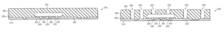
- FIG. 4 illustrates a molding process being performed on partially fabricated device 200 of FIG. 3 in accordance with an exemplary embodiment of the invention.
- An encapsulant 240 which may be made of epoxy, epoxy resin compound, or other encapsulating material known in the art, is molded around at least a portion of die 230 , attachment pads 235 , and side two 220 of conductive plate 205 .
- encapsulant 240 exhibits high strength and low shrinkage during curing, and protects die 230 , attachment pads 235 , and the electrical connections between die 230 and conductive plate 205 when encapsulant 240 is sufficiently cured and hardened.
- conductive layers and connections may be added on a surface 245 of encapsulant 240 , exemplary embodiments of which are shown in FIGS. 5 and 6 . If no additional layers are required, partially fabricated device 200 of FIG. 4 is processed to form conductive traces as shown in FIG. 7A .
- FIG. 5 shows a side elevational view of vias 250 and thermal vias 255 being formed in partially fabricated device 200 of FIG. 4 in accordance with an exemplary embodiment of the invention.
- Vias 250 and thermal vias 255 may be formed by chemical or mechanical reaming, drilling, milling, or the like.
- vias 250 and thermal vias 255 are shown in FIGS. 5 , 6 , 7 B, 8 B, and 10 as blind vias.
- vias 250 and thermal vias 255 may also be through holes, buried vias, or the like.
- a conductive material is deposited on surface 245 , vias 250 , and thermal vias 255 and patterned on partially fabricated device 200 of FIG. 5 in accordance with an exemplary embodiment of the invention.
- the conductive material may be copper, gold, silver, aluminum, copper alloys, or other suitable electrical and/or thermal conductors, and deposited on surface 245 , vias 250 , and thermal vias 255 by sputtering, chemical deposition, or other deposition methods known in the art.
- the conductive material may then be patterned to form conductive traces on encapsulant surface 245 using photolithography, etching, stamping, embossing, grinding, polishing, or other processes known in the art.
- encapsulant surface 245 provides exposed connectors that may be aligned with and connected to the conductive traces of overlaying IC packages to form a stack 1000 as shown in FIG. 10 and described hereinafter.
- encapsulant surface 245 and/or the conductive traces thereon may be further processed, such as coating with solder, solder resist and/or mask, thermal paste, adhesive, and the like.
- FIG. 7A is a side elevational view of a metal web being formed by removing material from side one 210 of conductive plate 205 of partially fabricated device 200 of FIG. 4 in accordance with an exemplary embodiment of the invention.
- FIG. 7B is a side elevational view of a metal web being formed by removing material from side one 210 of conductive plate 205 of partially fabricated device 200 of FIG. 6 also in accordance with an exemplary embodiment of the invention.
- conductive plate 205 Prior to forming the metal web of conductive traces and connections, may be patterned on side one 210 to form additional conductive traces and connections.
- Formation of the metal web may be accomplished by etching, polishing, grinding, or otherwise removing an amount of material from side one 210 sufficient to form conductive traces and/or connections previously patterned onto side two 220 and/or side one 210 of conductive plate 205 .
- the amount of material removed may be predetermined and/or based on measurements of the characteristics (e.g., mass, conductivity, thickness, and the like) of partially fabricated device 200 or parts thereof made during fabrication.
- a layer of solder mask 260 may be screened onto side one 210 of partially fabricated device 200 to protect the formed conductive traces and/or connections.
- FIG. 8A illustrates an IC package 290 formed by singulating (e.g., dividing, partitioning, and the like) partially fabricated device 200 of FIG. 7A in accordance with an exemplary embodiment of the invention.
- FIG. 8B illustrates an IC package 290 formed by singulating partially fabricated device 200 of FIG. 7B also in accordance with an exemplary embodiment of the invention.
- FIG. 8C illustrates a top plan view of IC package 290 formed by singulating partially fabricated device 200 of FIG. 7A or FIG. 7B in accordance with various embodiments of the invention.
- the singulation process may be performed by chemical, mechanical, or laser cutting, sawing, punching, slicing, stamping, and the like.
- FIG. 9 is a side elevational view of partially fabricated device 200 in which die 230 has an exposed surface 250 not encapsulated by encapsulant 240 , in accordance to various embodiments of the invention. Having exposed surface 250 may enhance thermal management of the IC package, decrease the profile of the IC package, and/or permit visual identification of die 230 . Exposed surface 250 may be covered by an optically transparent and/or thermally conductive compound or a thermal sensor to prevent contaminants from coming in contact with die 230 and/or enhance thermal management of the IC package.
- FIG. 10 is a side elevational view of stack 1000 of partially fabricated top and bottom devices 200 and 201 , respectively, in accordance with an exemplary embodiment of the invention.
- Conductive material is deposited on surface 245 and vias 250 of bottom device 201 and patterned into conductive traces as shown in FIG. 6 , and material on side one 210 of top device 200 is removed to form a metal web of conductive traces and connections as shown in FIG. 7 .
- the conductive traces on side one 210 of top device 200 may then be aligned with and connected to the conductive traces on surface 245 of bottom device 201 to form stack 1000 .
- Stack 1000 may be further stacked with additional IC packages and is not limited to the exemplary embodiment illustrated in FIG. 10 .
- FIG. 11 is a top plan view of partially fabricated device 200 being singulated into packages and modules in accordance with an exemplary embodiment of the invention.
- partially fabricated device 200 may have modules 1100 and 1110 that each includes one or more dies 230 and circuit components 1120 of various sizes. Singulating modules (e.g., modules 1100 and 1110 ) from partially fabricated device 200 is straightforward because using conductive plate 205 as the substrate provides for greater flexibility to freely place dies 230 and/or components 1120 of various sizes anywhere on conductive plate 205 and to group any number of dies 230 and/or components 1120 into one or more modules of various sizes and shapes.
- the modules may have geometric shapes (e.g., module 1100 ) or non-geometric shapes (e.g., module 1110 ).
- conductive plate 205 may be patterned, or have material selectively removed through part of its thickness, to form partial patterns.
- the partial patterns serve as the basis from which conductive traces and/or connections are formed, including those between dies 230 and components 1120 in modules 1100 and 1110 as shown in FIG. 11 .
- an amount of material may be removed from patterned conductive plate 205 to form a metal web of conductive traces and/or connections based on the partial pattern.
- Partially fabricated device 200 having conductive plate 205 that includes modules 1100 and 1110 may also be further processed as described above in accordance with various embodiments.
Abstract
Description
Claims (20)
Priority Applications (2)
| Application Number | Priority Date | Filing Date | Title |
|---|---|---|---|
| US12/116,459 US8039309B2 (en) | 2007-05-10 | 2008-05-07 | Systems and methods for post-circuitization assembly |
| PCT/US2008/063406 WO2008141273A1 (en) | 2007-05-10 | 2008-05-12 | Systems and methods for post-circuitization assembly |
Applications Claiming Priority (2)
| Application Number | Priority Date | Filing Date | Title |
|---|---|---|---|
| US92857207P | 2007-05-10 | 2007-05-10 | |
| US12/116,459 US8039309B2 (en) | 2007-05-10 | 2008-05-07 | Systems and methods for post-circuitization assembly |
Publications (2)
| Publication Number | Publication Date |
|---|---|
| US20080280394A1 US20080280394A1 (en) | 2008-11-13 |
| US8039309B2 true US8039309B2 (en) | 2011-10-18 |
Family
ID=39969899
Family Applications (1)
| Application Number | Title | Priority Date | Filing Date |
|---|---|---|---|
| US12/116,459 Active 2029-02-23 US8039309B2 (en) | 2007-05-10 | 2008-05-07 | Systems and methods for post-circuitization assembly |
Country Status (2)
| Country | Link |
|---|---|
| US (1) | US8039309B2 (en) |
| WO (1) | WO2008141273A1 (en) |
Cited By (3)
| Publication number | Priority date | Publication date | Assignee | Title |
|---|---|---|---|---|
| EP2367033A1 (en) | 2008-01-14 | 2011-09-21 | Avery Dennison Corporation | Retroreflector for use in touch screen applications and positions sensing system |
| US20120126423A1 (en) * | 2010-11-23 | 2012-05-24 | Shinko Electric Industries Co., Ltd. | Semiconductor device manufacturing method and semiconductor device |
| US10431648B2 (en) | 2014-05-02 | 2019-10-01 | Invensas Corporation | Making electrical components in handle wafers of integrated circuit packages |
Families Citing this family (18)
| Publication number | Priority date | Publication date | Assignee | Title |
|---|---|---|---|---|
| US8021907B2 (en) * | 2008-06-09 | 2011-09-20 | Stats Chippac, Ltd. | Method and apparatus for thermally enhanced semiconductor package |
| US7989950B2 (en) * | 2008-08-14 | 2011-08-02 | Stats Chippac Ltd. | Integrated circuit packaging system having a cavity |
| US8823160B2 (en) * | 2008-08-22 | 2014-09-02 | Stats Chippac Ltd. | Integrated circuit package system having cavity |
| JP2010262992A (en) * | 2009-04-30 | 2010-11-18 | Sanyo Electric Co Ltd | Semiconductor module and portable apparatus |
| US8319318B2 (en) * | 2010-04-06 | 2012-11-27 | Intel Corporation | Forming metal filled die back-side film for electromagnetic interference shielding with coreless packages |
| US8618652B2 (en) * | 2010-04-16 | 2013-12-31 | Intel Corporation | Forming functionalized carrier structures with coreless packages |
| DK2610255T3 (en) * | 2010-08-25 | 2016-05-30 | Neopharm Co Ltd | 1H-benzo [d] imidazol-5-yl compounds and a composition for the treatment of inflammatory diseases |
| US8304913B2 (en) * | 2010-09-24 | 2012-11-06 | Intel Corporation | Methods of forming fully embedded bumpless build-up layer packages and structures formed thereby |
| US8546193B2 (en) * | 2010-11-02 | 2013-10-01 | Stats Chippac, Ltd. | Semiconductor device and method of forming penetrable film encapsulant around semiconductor die and interconnect structure |
| US8736065B2 (en) | 2010-12-22 | 2014-05-27 | Intel Corporation | Multi-chip package having a substrate with a plurality of vertically embedded die and a process of forming the same |
| WO2013176662A1 (en) * | 2012-05-23 | 2013-11-28 | Intel Corporation | Multi-stacked bbul package |
| US20150115420A1 (en) * | 2013-10-31 | 2015-04-30 | Navas Khan Oratti Kalandar | Sensor die grid array package |
| US20150262902A1 (en) | 2014-03-12 | 2015-09-17 | Invensas Corporation | Integrated circuits protected by substrates with cavities, and methods of manufacture |
| US9355997B2 (en) | 2014-03-12 | 2016-05-31 | Invensas Corporation | Integrated circuit assemblies with reinforcement frames, and methods of manufacture |
| US9741649B2 (en) | 2014-06-04 | 2017-08-22 | Invensas Corporation | Integrated interposer solutions for 2D and 3D IC packaging |
| US9252127B1 (en) | 2014-07-10 | 2016-02-02 | Invensas Corporation | Microelectronic assemblies with integrated circuits and interposers with cavities, and methods of manufacture |
| US9478504B1 (en) | 2015-06-19 | 2016-10-25 | Invensas Corporation | Microelectronic assemblies with cavities, and methods of fabrication |
| US20200161206A1 (en) * | 2018-11-20 | 2020-05-21 | Advanced Semiconductor Engineering, Inc. | Semiconductor package structure and semiconductor manufacturing process |
Citations (11)
| Publication number | Priority date | Publication date | Assignee | Title |
|---|---|---|---|---|
| US5618752A (en) * | 1995-06-05 | 1997-04-08 | Harris Corporation | Method of fabrication of surface mountable integrated circuits |
| JPH09221375A (en) | 1996-02-14 | 1997-08-26 | Sumitomo Metal Ind Ltd | Ceramic substrate and its manufacture |
| JPH09307238A (en) | 1996-05-20 | 1997-11-28 | Kyocera Corp | Multilayer circuit board |
| US5976769A (en) * | 1995-07-14 | 1999-11-02 | Texas Instruments Incorporated | Intermediate layer lithography |
| JP2003282785A (en) | 2002-03-26 | 2003-10-03 | Kyocera Corp | High-frequency circuit multilayer board |
| US6809421B1 (en) * | 1996-12-02 | 2004-10-26 | Kabushiki Kaisha Toshiba | Multichip semiconductor device, chip therefor and method of formation thereof |
| US20050186705A1 (en) * | 2002-07-31 | 2005-08-25 | Jackson Timothy L. | Semiconductor dice having backside redistribution layer accessed using through-silicon vias, methods |
| US20060012048A1 (en) | 2004-07-07 | 2006-01-19 | Nec Corporation And Nec Electronics Corporation | Wiring substrate for mounting semiconductors, method of manufacturing the same, and semiconductor package |
| US20070262328A1 (en) * | 2006-05-10 | 2007-11-15 | Nichia Corporation | Semiconductor light emitting device and a method for producing the same |
| US20090263936A1 (en) * | 2005-08-29 | 2009-10-22 | Toyohiko Fujisawa | Insulating Liquid Die-Bonding Agent And Semiconductor Device |
| US20100224890A1 (en) * | 2006-09-18 | 2010-09-09 | Cree, Inc. | Light emitting diode chip with electrical insulation element |
Family Cites Families (3)
| Publication number | Priority date | Publication date | Assignee | Title |
|---|---|---|---|---|
| JPH07273455A (en) * | 1994-03-30 | 1995-10-20 | Oki Electric Ind Co Ltd | Ceramic multilayer substrate and manufacturing method thereof |
| US6137161A (en) * | 1999-09-14 | 2000-10-24 | International Business Machines Corporation | Interposer array module for capacitive decoupling and filtering |
| JP2005236220A (en) * | 2004-02-23 | 2005-09-02 | Dainippon Printing Co Ltd | Wiring substrate and its manufacturing method, and semiconductor package |
-
2008
- 2008-05-07 US US12/116,459 patent/US8039309B2/en active Active
- 2008-05-12 WO PCT/US2008/063406 patent/WO2008141273A1/en active Application Filing
Patent Citations (11)
| Publication number | Priority date | Publication date | Assignee | Title |
|---|---|---|---|---|
| US5618752A (en) * | 1995-06-05 | 1997-04-08 | Harris Corporation | Method of fabrication of surface mountable integrated circuits |
| US5976769A (en) * | 1995-07-14 | 1999-11-02 | Texas Instruments Incorporated | Intermediate layer lithography |
| JPH09221375A (en) | 1996-02-14 | 1997-08-26 | Sumitomo Metal Ind Ltd | Ceramic substrate and its manufacture |
| JPH09307238A (en) | 1996-05-20 | 1997-11-28 | Kyocera Corp | Multilayer circuit board |
| US6809421B1 (en) * | 1996-12-02 | 2004-10-26 | Kabushiki Kaisha Toshiba | Multichip semiconductor device, chip therefor and method of formation thereof |
| JP2003282785A (en) | 2002-03-26 | 2003-10-03 | Kyocera Corp | High-frequency circuit multilayer board |
| US20050186705A1 (en) * | 2002-07-31 | 2005-08-25 | Jackson Timothy L. | Semiconductor dice having backside redistribution layer accessed using through-silicon vias, methods |
| US20060012048A1 (en) | 2004-07-07 | 2006-01-19 | Nec Corporation And Nec Electronics Corporation | Wiring substrate for mounting semiconductors, method of manufacturing the same, and semiconductor package |
| US20090263936A1 (en) * | 2005-08-29 | 2009-10-22 | Toyohiko Fujisawa | Insulating Liquid Die-Bonding Agent And Semiconductor Device |
| US20070262328A1 (en) * | 2006-05-10 | 2007-11-15 | Nichia Corporation | Semiconductor light emitting device and a method for producing the same |
| US20100224890A1 (en) * | 2006-09-18 | 2010-09-09 | Cree, Inc. | Light emitting diode chip with electrical insulation element |
Cited By (3)
| Publication number | Priority date | Publication date | Assignee | Title |
|---|---|---|---|---|
| EP2367033A1 (en) | 2008-01-14 | 2011-09-21 | Avery Dennison Corporation | Retroreflector for use in touch screen applications and positions sensing system |
| US20120126423A1 (en) * | 2010-11-23 | 2012-05-24 | Shinko Electric Industries Co., Ltd. | Semiconductor device manufacturing method and semiconductor device |
| US10431648B2 (en) | 2014-05-02 | 2019-10-01 | Invensas Corporation | Making electrical components in handle wafers of integrated circuit packages |
Also Published As
| Publication number | Publication date |
|---|---|
| WO2008141273A1 (en) | 2008-11-20 |
| US20080280394A1 (en) | 2008-11-13 |
Similar Documents
| Publication | Publication Date | Title |
|---|---|---|
| US8039309B2 (en) | Systems and methods for post-circuitization assembly | |
| US10796970B2 (en) | Method for fabricating electronic package | |
| US6818998B2 (en) | Stacked chip package having upper chip provided with trenches and method of manufacturing the same | |
| US7754530B2 (en) | Thermal enhanced low profile package structure and method for fabricating the same | |
| TWI466244B (en) | Method of making stackable semiconductor assembly with bump/flange heat spreader and dual build-up circuitry | |
| US11410899B2 (en) | Semiconductor package device and method of manufacturing the same | |
| US7344969B2 (en) | Stacked die in die BGA package | |
| US7833840B2 (en) | Integrated circuit package system with down-set die pad and method of manufacture thereof | |
| US20070170583A1 (en) | Multilayer integrated circuit for RF communication and method for assembly thereof | |
| US20030156402A1 (en) | Method for making a build-up package of a semiconductor die and structure formed from the same | |
| US8168473B2 (en) | Molded ultra thin semiconductor die packages, systems using the same, and methods of making the same | |
| CN103681468A (en) | Semiconductor device and method of forming dual-sided interconnect structures in Fo-WLCSP | |
| US6879034B1 (en) | Semiconductor package including low temperature co-fired ceramic substrate | |
| EP3147942B1 (en) | Semiconductor package, semiconductor device using the same and manufacturing method thereof | |
| US20100190294A1 (en) | Methods for controlling wafer and package warpage during assembly of very thin die | |
| CN112447534A (en) | Package and method for manufacturing the same | |
| US7678610B2 (en) | Semiconductor chip package and method of manufacture | |
| US20090124048A1 (en) | Semiconductor device and method of manufacturing semiconductor device | |
| US20170047262A1 (en) | Electronic package and fabrication method thereof | |
| US9761570B1 (en) | Electronic component package with multple electronic components | |
| US20050275081A1 (en) | Embedded chip semiconductor having dual electronic connection faces | |
| CN113257773A (en) | Semiconductor device package and method of manufacturing the same | |
| US11329016B2 (en) | Semiconductor device package and method of manufacturing the same | |
| US20160104652A1 (en) | Package structure and method of fabricating the same | |
| US20230207729A1 (en) | Semiconductor device package and method of manufacturing the same |
Legal Events
| Date | Code | Title | Description |
|---|---|---|---|
| AS | Assignment |
Owner name: TEXAS INSTRUMENTS INCORPORATED, TEXAS Free format text: ASSIGNMENT OF ASSIGNORS INTEREST;ASSIGNORS:MURTUZA, MASOOD;CHAUHAN, SATYENDRA SINGH;ABBOTT, DONALD C.;REEL/FRAME:020913/0390 Effective date: 20080506 |
|
| STCF | Information on status: patent grant |
Free format text: PATENTED CASE |
|
| FPAY | Fee payment |
Year of fee payment: 4 |
|
| MAFP | Maintenance fee payment |
Free format text: PAYMENT OF MAINTENANCE FEE, 8TH YEAR, LARGE ENTITY (ORIGINAL EVENT CODE: M1552); ENTITY STATUS OF PATENT OWNER: LARGE ENTITY Year of fee payment: 8 |
|
| MAFP | Maintenance fee payment |
Free format text: PAYMENT OF MAINTENANCE FEE, 12TH YEAR, LARGE ENTITY (ORIGINAL EVENT CODE: M1553); ENTITY STATUS OF PATENT OWNER: LARGE ENTITY Year of fee payment: 12 |