US8039841B2 - Organic light emitting diode display - Google Patents
Organic light emitting diode display Download PDFInfo
- Publication number
- US8039841B2 US8039841B2 US12/347,053 US34705308A US8039841B2 US 8039841 B2 US8039841 B2 US 8039841B2 US 34705308 A US34705308 A US 34705308A US 8039841 B2 US8039841 B2 US 8039841B2
- Authority
- US
- United States
- Prior art keywords
- disposed
- organic light
- electrode
- common voltage
- insulating layer
- Prior art date
- Legal status (The legal status is an assumption and is not a legal conclusion. Google has not performed a legal analysis and makes no representation as to the accuracy of the status listed.)
- Expired - Fee Related, expires
Links
- 239000010409 thin film Substances 0.000 claims abstract description 39
- 239000000758 substrate Substances 0.000 claims abstract description 14
- 229910052751 metal Inorganic materials 0.000 claims description 8
- 239000002184 metal Substances 0.000 claims description 8
- 239000010410 layer Substances 0.000 description 94
- 238000002161 passivation Methods 0.000 description 23
- 239000004065 semiconductor Substances 0.000 description 15
- 238000004519 manufacturing process Methods 0.000 description 10
- 238000005192 partition Methods 0.000 description 10
- 239000012212 insulator Substances 0.000 description 8
- 238000000034 method Methods 0.000 description 8
- 239000000463 material Substances 0.000 description 6
- 229910021417 amorphous silicon Inorganic materials 0.000 description 5
- 239000003086 colorant Substances 0.000 description 5
- 238000000151 deposition Methods 0.000 description 5
- 239000011368 organic material Substances 0.000 description 5
- 238000000059 patterning Methods 0.000 description 5
- 239000003990 capacitor Substances 0.000 description 4
- 238000000206 photolithography Methods 0.000 description 4
- 238000003860 storage Methods 0.000 description 4
- BQCADISMDOOEFD-UHFFFAOYSA-N Silver Chemical compound [Ag] BQCADISMDOOEFD-UHFFFAOYSA-N 0.000 description 3
- 229910052782 aluminium Inorganic materials 0.000 description 3
- XAGFODPZIPBFFR-UHFFFAOYSA-N aluminium Chemical compound [Al] XAGFODPZIPBFFR-UHFFFAOYSA-N 0.000 description 3
- 230000003247 decreasing effect Effects 0.000 description 3
- 238000010586 diagram Methods 0.000 description 3
- 238000005530 etching Methods 0.000 description 3
- 238000002513 implantation Methods 0.000 description 3
- 230000008569 process Effects 0.000 description 3
- 229910052709 silver Inorganic materials 0.000 description 3
- 239000004332 silver Substances 0.000 description 3
- 239000012780 transparent material Substances 0.000 description 3
- 229910052581 Si3N4 Inorganic materials 0.000 description 2
- VYPSYNLAJGMNEJ-UHFFFAOYSA-N Silicium dioxide Chemical compound O=[Si]=O VYPSYNLAJGMNEJ-UHFFFAOYSA-N 0.000 description 2
- 239000011575 calcium Substances 0.000 description 2
- 239000010408 film Substances 0.000 description 2
- 230000006870 function Effects 0.000 description 2
- 239000011777 magnesium Substances 0.000 description 2
- 230000003287 optical effect Effects 0.000 description 2
- 239000012044 organic layer Substances 0.000 description 2
- HQVNEWCFYHHQES-UHFFFAOYSA-N silicon nitride Chemical compound N12[Si]34N5[Si]62N3[Si]51N64 HQVNEWCFYHHQES-UHFFFAOYSA-N 0.000 description 2
- 229910052814 silicon oxide Inorganic materials 0.000 description 2
- OYPRJOBELJOOCE-UHFFFAOYSA-N Calcium Chemical compound [Ca] OYPRJOBELJOOCE-UHFFFAOYSA-N 0.000 description 1
- VYZAMTAEIAYCRO-UHFFFAOYSA-N Chromium Chemical compound [Cr] VYZAMTAEIAYCRO-UHFFFAOYSA-N 0.000 description 1
- FYYHWMGAXLPEAU-UHFFFAOYSA-N Magnesium Chemical compound [Mg] FYYHWMGAXLPEAU-UHFFFAOYSA-N 0.000 description 1
- OAICVXFJPJFONN-UHFFFAOYSA-N Phosphorus Chemical compound [P] OAICVXFJPJFONN-UHFFFAOYSA-N 0.000 description 1
- XUIMIQQOPSSXEZ-UHFFFAOYSA-N Silicon Chemical compound [Si] XUIMIQQOPSSXEZ-UHFFFAOYSA-N 0.000 description 1
- 229910045601 alloy Inorganic materials 0.000 description 1
- 239000000956 alloy Substances 0.000 description 1
- 229910052788 barium Inorganic materials 0.000 description 1
- DSAJWYNOEDNPEQ-UHFFFAOYSA-N barium atom Chemical compound [Ba] DSAJWYNOEDNPEQ-UHFFFAOYSA-N 0.000 description 1
- 230000015572 biosynthetic process Effects 0.000 description 1
- 229910052791 calcium Inorganic materials 0.000 description 1
- 230000008859 change Effects 0.000 description 1
- 229910052804 chromium Inorganic materials 0.000 description 1
- 239000011651 chromium Substances 0.000 description 1
- 150000001875 compounds Chemical class 0.000 description 1
- 239000004020 conductor Substances 0.000 description 1
- 230000006866 deterioration Effects 0.000 description 1
- 238000001312 dry etching Methods 0.000 description 1
- 230000005669 field effect Effects 0.000 description 1
- 239000011521 glass Substances 0.000 description 1
- 239000007943 implant Substances 0.000 description 1
- 239000012535 impurity Substances 0.000 description 1
- AMGQUBHHOARCQH-UHFFFAOYSA-N indium;oxotin Chemical compound [In].[Sn]=O AMGQUBHHOARCQH-UHFFFAOYSA-N 0.000 description 1
- 229910052749 magnesium Inorganic materials 0.000 description 1
- 239000011159 matrix material Substances 0.000 description 1
- 150000002739 metals Chemical class 0.000 description 1
- 230000004048 modification Effects 0.000 description 1
- 238000012986 modification Methods 0.000 description 1
- 239000011574 phosphorus Substances 0.000 description 1
- 229910052698 phosphorus Inorganic materials 0.000 description 1
- 239000000049 pigment Substances 0.000 description 1
- -1 region Substances 0.000 description 1
- 230000004044 response Effects 0.000 description 1
- 229910052710 silicon Inorganic materials 0.000 description 1
- 239000010703 silicon Substances 0.000 description 1
- 230000002194 synthesizing effect Effects 0.000 description 1
- YVTHLONGBIQYBO-UHFFFAOYSA-N zinc indium(3+) oxygen(2-) Chemical compound [O--].[Zn++].[In+3] YVTHLONGBIQYBO-UHFFFAOYSA-N 0.000 description 1
Images


Classifications
-
- H—ELECTRICITY
- H10—SEMICONDUCTOR DEVICES; ELECTRIC SOLID-STATE DEVICES NOT OTHERWISE PROVIDED FOR
- H10K—ORGANIC ELECTRIC SOLID-STATE DEVICES
- H10K59/00—Integrated devices, or assemblies of multiple devices, comprising at least one organic light-emitting element covered by group H10K50/00
- H10K59/10—OLED displays
- H10K59/12—Active-matrix OLED [AMOLED] displays
- H10K59/123—Connection of the pixel electrodes to the thin film transistors [TFT]
-
- H—ELECTRICITY
- H10—SEMICONDUCTOR DEVICES; ELECTRIC SOLID-STATE DEVICES NOT OTHERWISE PROVIDED FOR
- H10K—ORGANIC ELECTRIC SOLID-STATE DEVICES
- H10K59/00—Integrated devices, or assemblies of multiple devices, comprising at least one organic light-emitting element covered by group H10K50/00
- H10K59/10—OLED displays
- H10K59/12—Active-matrix OLED [AMOLED] displays
- H10K59/121—Active-matrix OLED [AMOLED] displays characterised by the geometry or disposition of pixel elements
-
- H—ELECTRICITY
- H10—SEMICONDUCTOR DEVICES; ELECTRIC SOLID-STATE DEVICES NOT OTHERWISE PROVIDED FOR
- H10K—ORGANIC ELECTRIC SOLID-STATE DEVICES
- H10K59/00—Integrated devices, or assemblies of multiple devices, comprising at least one organic light-emitting element covered by group H10K50/00
- H10K59/30—Devices specially adapted for multicolour light emission
- H10K59/35—Devices specially adapted for multicolour light emission comprising red-green-blue [RGB] subpixels
-
- H—ELECTRICITY
- H10—SEMICONDUCTOR DEVICES; ELECTRIC SOLID-STATE DEVICES NOT OTHERWISE PROVIDED FOR
- H10K—ORGANIC ELECTRIC SOLID-STATE DEVICES
- H10K59/00—Integrated devices, or assemblies of multiple devices, comprising at least one organic light-emitting element covered by group H10K50/00
- H10K59/80—Constructional details
- H10K59/875—Arrangements for extracting light from the devices
- H10K59/878—Arrangements for extracting light from the devices comprising reflective means
-
- H—ELECTRICITY
- H01—ELECTRIC ELEMENTS
- H01L—SEMICONDUCTOR DEVICES NOT COVERED BY CLASS H10
- H01L27/00—Devices consisting of a plurality of semiconductor or other solid-state components formed in or on a common substrate
- H01L27/02—Devices consisting of a plurality of semiconductor or other solid-state components formed in or on a common substrate including semiconductor components specially adapted for rectifying, oscillating, amplifying or switching and having at least one potential-jump barrier or surface barrier; including integrated passive circuit elements with at least one potential-jump barrier or surface barrier
- H01L27/04—Devices consisting of a plurality of semiconductor or other solid-state components formed in or on a common substrate including semiconductor components specially adapted for rectifying, oscillating, amplifying or switching and having at least one potential-jump barrier or surface barrier; including integrated passive circuit elements with at least one potential-jump barrier or surface barrier the substrate being a semiconductor body
- H01L27/10—Devices consisting of a plurality of semiconductor or other solid-state components formed in or on a common substrate including semiconductor components specially adapted for rectifying, oscillating, amplifying or switching and having at least one potential-jump barrier or surface barrier; including integrated passive circuit elements with at least one potential-jump barrier or surface barrier the substrate being a semiconductor body including a plurality of individual components in a repetitive configuration
- H01L27/118—Masterslice integrated circuits
- H01L27/11803—Masterslice integrated circuits using field effect technology
- H01L27/11807—CMOS gate arrays
- H01L2027/11868—Macro-architecture
- H01L2027/11874—Layout specification, i.e. inner core region
- H01L2027/11879—Data lines (buses)
-
- H—ELECTRICITY
- H01—ELECTRIC ELEMENTS
- H01L—SEMICONDUCTOR DEVICES NOT COVERED BY CLASS H10
- H01L2924/00—Indexing scheme for arrangements or methods for connecting or disconnecting semiconductor or solid-state bodies as covered by H01L24/00
- H01L2924/10—Details of semiconductor or other solid state devices to be connected
- H01L2924/11—Device type
- H01L2924/13—Discrete devices, e.g. 3 terminal devices
- H01L2924/1304—Transistor
- H01L2924/1306—Field-effect transistor [FET]
- H01L2924/13069—Thin film transistor [TFT]
-
- H—ELECTRICITY
- H10—SEMICONDUCTOR DEVICES; ELECTRIC SOLID-STATE DEVICES NOT OTHERWISE PROVIDED FOR
- H10K—ORGANIC ELECTRIC SOLID-STATE DEVICES
- H10K50/00—Organic light-emitting devices
- H10K50/80—Constructional details
- H10K50/85—Arrangements for extracting light from the devices
- H10K50/856—Arrangements for extracting light from the devices comprising reflective means
Definitions
- This disclosure relates to an organic light-emitting diode (“OLED”) display.
- OLED organic light-emitting diode
- An OLED display includes a plurality of organic light-emitting elements and a plurality of thin film transistors (“TFT”s), which control the organic light-emitting elements.
- a TFT includes a plurality of thin films and can be disposed at a lower side of an OLED display, while an organic light-emitting element can be disposed at an upper side of the OLED display.
- An anode of the organic light-emitting element can be disposed at the lower side of the OLED display, and a cathode of the organic light-emitting element can be disposed at the upper side of the OLED display.
- An OLED display may be classified as a top emission type, which emits light upward, and a bottom emission type, which emits light downward.
- a bottom emission OLED display an area where light is emitted is decreased due to the TFTs disposed under the organic light-emitting elements, therefore the top emission type can have a more desirable aperture ratio.
- a bottom emission OLED display can include a spot due to optical interference, which can occur when light passes through the thin films.
- a top emission OLED display includes very few thin films on the light path, thus substantially reducing or preventing a spot.
- Identifying a suitable transparent material that satisfies the work function requirements for a cathode in a top emission OLED display is difficult. Therefore a very thin film of an opaque metal can be disposed for use as the cathode while allowing for the passage of light. A resistance of a very thin film cathode can be large. To address the high resistance of a thin film cathode, an additional common voltage line for transmitting a common voltage can be disposed on the substrate and electrically connected to the cathode of the organic light-emitting element.
- an organic light-emitting diode (“OLED”) display including: a first thin film transistor disposed on a substrate; a first insulating layer disposed on the first thin film transistor; a reflective electrode disposed on the first insulating layer; a common voltage line disposed on the first insulating layer and separated from the reflective electrode; a second insulating layer disposed on the reflective electrode and the common voltage line; a pixel electrode disposed on the second insulating layer and electrically connected to the first thin film transistor; an organic light-emitting member disposed on the pixel electrode; and a common electrode disposed on the organic light-emitting member, wherein the common voltage line is electrically connected to the common electrode.
- OLED organic light-emitting diode
- an OLED wherein the second insulating layer has a first contact hole which exposes the common voltage line, and the common electrode is electrically connected to the common voltage line through the first contact hole.
- an OLED further including a second thin film transistor disposed under the first insulating layer, and a connection member disposed on the first insulating layer and electrically connecting the first thin film transistor and the second thin film transistor.
- an OLED wherein the pixel electrode overlaps the reflective electrode and the connection member.
- an OLED display further including a gate line and a data line disposed under the first insulating layer, the gate line and the data line electrically connected to the second thin film transistor, wherein the common voltage line overlaps the gate line and the data line.
- the common voltage line overlaps the second thin film transistor.
- an OLED display further including a contact assistance member disposed on the second insulating layer, the contact assistance member contacting the common voltage line and the common electrode.
- the common voltage line includes a net-like shape
- the reflective electrode is disposed in a region defined by the net-like shape
- the common electrode includes a metal
- a method for manufacturing an OLED display includes: forming a thin film transistor including a control electrode, an input electrode, and an output electrode on a substrate; depositing a passivation layer on the thin film transistor; patterning the passivation layer to form a first contact hole which exposes the output electrode; forming a reflective electrode electrically connected to the output electrode through the first contact hole; forming a common voltage line separated from the reflective electrode and on the passivation layer; depositing an insulating layer on the reflective electrode and the common voltage line; patterning the insulating layer to form a second contact hole, which exposes a portion of the reflective electrode; and patterning the insulating layer to form a third contact hole, which exposes a portion of the common voltage line; forming a pixel electrode electrically connected to the reflective electrode through the second contact hole; forming an organic light-emitting member on the pixel electrode; and forming a common electrode electrically connected to the common voltage line through the third contact hole.
- an organic light-emitting diode display including: forming a thin film transistor including a control electrode, an input electrode, and an output electrode on a substrate; depositing a passivation layer on the thin film transistor; patterning the passivation layer to form a first contact hole, which exposes the output electrode, and a second contact hole, which exposes the input electrode; forming a reflective electrode electrically connected to the output electrode through the first contact hole; forming a driving voltage line electrically connected to the input electrode through the second contact hole; depositing an insulating layer on the reflective electrode and the driving voltage line; patterning the insulating layer to form a third contact hole which exposes a portion of the reflective electrode; forming a pixel electrode electrically connected to the reflective electrode through the through the third contact hole; forming an organic light-emitting member on the pixel electrode; and forming a common electrode on the organic light-emitting member and the insulating layer.
- FIG. 1 is an equivalent circuit diagram showing an exemplary embodiment of an organic light-emitting diode (“OLED”) display
- FIG. 2 is a plan view showing an exemplary embodiment of an OLED display
- FIG. 3 is a plan view showing an exemplary embodiment of a portion of the OLED display shown in FIG. 2 ;
- FIG. 4 is a cross-sectional view showing an exemplary embodiment of the OLED display shown in FIG. 2 taken along line IV-IV;
- FIG. 5 is a cross-sectional view showing another exemplary embodiment of the OLED display shown in FIG. 2 taken along line IV-IV;
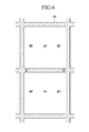
- FIG. 6 is a plan view showing another exemplary embodiment of an OLED display
- FIG. 7 to FIG. 16 are cross-sectional views showing exemplary embodiments of intermediate steps of a manufacturing process of the OLED display shown in FIG. 2 to FIG. 5 ;
- FIG. 17 is a cross-sectional view showing another exemplary embodiment of an OLED display.
- first, second, third, etc. may be used herein to describe various elements, components, regions, layers and/or sections, these elements, components, regions, layers and/or sections should not be limited by these terms. These terms are only used to distinguish one element, component, region, layer, or section from another region, layer or section. Thus, a first element, component, region, layer, or section discussed below could be termed a second element, component, region, layer, or section without departing from the teachings of the present invention.
- spatially relative terms such as “lower,” “under,” “upper” and the like, may be used herein for ease of description to describe the relationship of one element or feature to another element(s) or feature(s) as illustrated in the figures. It will be understood that the spatially relative terms are intended to encompass different orientations of the device in use or operation, in addition to the orientation depicted in the figures. For example, if the device in the figures is turned over, elements described as “lower” or “under” relative to other elements or features would then be oriented “upper” or “over” relative to the other elements or features. Thus, the exemplary term “under” can encompass both an orientation of above and below. The device may be otherwise oriented (rotated 90 degrees or at other orientations) and the spatially relative descriptors used herein interpreted accordingly.
- Embodiments are described herein with reference to cross-section illustrations that are schematic illustrations of idealized embodiments (and intermediate structures) of the invention. As such, variations from the shapes of the illustrations as a result, for example, of manufacturing techniques and/or tolerances, are to be expected. Thus, embodiments should not be construed as limited to the particular shapes of regions illustrated herein but are to include deviations in shapes that result, for example, from manufacturing.
- an implanted region illustrated as a rectangle will, typically, have rounded or curved features and/or a gradient of implant concentration at its edges rather than a binary change from implanted to non-implanted region.
- a buried region formed by implantation may result in some implantation in the region between the buried region and the surface through which the implantation takes place.
- the regions illustrated in the figures are schematic in nature and their shapes are not intended to illustrate the actual shape of a region of a device and are not intended to limit the scope of the invention.
- OLED organic light-emitting diode
- FIG. 1 is an equivalent circuit diagram showing an exemplary embodiment of an OLED display.
- an OLED display includes a plurality of signal lines 121 , 171 , 172 , and 332 , and a plurality of pixels PX electrically connected thereto and arranged substantially in a matrix.
- the signal lines include a plurality of gate lines 121 for transmitting gate signals (or scanning signals), a plurality of data lines 171 for transmitting data signals, a plurality of first driving voltage lines 172 for transmitting a driving voltage, and a plurality of common voltage lines 332 for transmitting a common voltage.
- the gate lines 121 extend substantially in a row direction and are substantially parallel to each other, and the data lines 171 extend substantially in a column direction and are substantially parallel to each other.
- the first driving voltage lines 172 extend substantially in the column direction, and the common voltage lines 332 comprise a net-like shape, thus can form a network.
- the net-like shape can be analogous to that of the gate lines 121 and the data lines 171 shown in FIG. 1 .
- the common voltage lines 332 form a rectilinear network.
- the common voltage lines 332 may respectively extend in the row direction or the column direction.
- Each pixel PX includes a switching transistor Qs, a driving transistor Qd, a storage capacitor Cst, and an organic light-emitting element LD.
- the switching transistor Qs comprises a control terminal, which is electrically connected to a gate line 121 , an input terminal, which is electrically connected to a data line 171 , and an output terminal, which is electrically connected to the driving transistor Qd.
- the switching transistor Qs transmits a data signal applied from the data line 171 to the driving transistor Qd in response to a gate signal applied from the gate line 121 .
- the driving transistor Qd has a control terminal electrically connected to the switching transistor Qs, an input terminal electrically connected to the first driving voltage line 172 , and an output terminal electrically connected to the organic light-emitting element.
- the driving transistor Qd drives an output current I LD , which has a magnitude which depends on the voltage between the control terminal and the output terminal.
- the storage capacitor Cst is electrically connected between the control terminal and the input terminal of the driving transistor Qd.
- the storage capacitor Cst stores a data voltage, which is also applied to the control terminal of the driving transistor Qd, and maintains the data voltage even after the switching transistor Qs turns off.
- the organic light-emitting element LD which can be an OLED, comprises an anode electrically connected to the output terminal of the driving transistor Qd, and a cathode electrically connected to the common voltage line 332 .
- the organic light-emitting element LD emits light having an intensity which depends on an output current I LD of the driving transistor Qd, thereby displaying an image.
- the switching transistor Qs and the driving transistor Qd can be an n-channel field effect transistor (“FET”), and may comprise the structure shown schematically in FIG. 1 .
- FET field effect transistor
- a switching transistor Qs and the driving transistor Qd may also be a p-channel FET.
- the connections among the transistors Qs and Qd, the capacitor Cst, and the organic light-emitting element LD, may be different.
- other transistors for compensating the threshold voltage of the driving transistor Qd may be further included in addition to the switching transistor Qs and the driving transistor Qd.
- FIG. 1 An equivalent circuit diagram of an OLED display is shown in FIG. 1 .
- the OLED display is further described with reference to FIG. 2 to FIG. 5 , as well as FIG. 1 .
- FIG. 2 is a plan view showing an exemplary embodiment of an OLED display
- FIG. 3 is a plan view showing an exemplary embodiment of the portion of the OLED display shown in FIG. 2
- FIG. 4 is a cross-sectional view showing an exemplary embodiment of the OLED display shown in FIG. 2 taken along line IV-IV
- FIG. 5 is a cross-sectional view showing an exemplary embodiment of the OLED display shown in FIG. 2 taken along line IV-IV.
- a gate line 121 including a first control electrode 124 a and a second control electrode 124 b , is disposed on an insulating substrate 110 .
- the insulating substrate 110 can comprise transparent glass, plastic, or the like, or a combination comprising at least one of the foregoing materials.
- the gate line 121 can extend substantially in a transverse direction, and the first control electrode 124 a can extend in an upward direction.
- the gate line 121 may include an end portion (not shown) and a large area for contact with another layer or an external driving circuit.
- the second control electrode 124 b can be separated from the gate line 121 and include a storage electrode 127 , which can extend in a longitudinal direction.
- a gate insulating layer 140 may comprise silicon oxide, silicon nitride, or the like, or a combination comprising at least one of the foregoing compounds, and can be disposed on the gate line and the second control electrode 124 b.
- a first and a second semiconductor islands 154 a and 154 b may comprise hydrogenated amorphous silicon, or the like, and are disposed on the gate insulating layer 140 .
- the first semiconductor island 154 a is disposed on the first control electrode 124
- the second semiconductor island 154 b is disposed on the second control electrode 124 b.
- a first pair of ohmic contacts 163 a and 165 a are disposed on the first semiconductor island 154 a
- a second pair of ohmic contacts 163 b and 165 b are disposed on the second semiconductor island 154 b
- the ohmic contacts 163 a , 163 b, 165 a , and 165 b can have an island shape and may comprise n+ hydrogenated amorphous silicon, or the like, which is heavily doped with an n-type impurity such as phosphorus, or the like.
- a data line 171 , a first driving voltage line 172 , a common voltage line 332 , and a first and a second output electrodes 175 a and 175 b are disposed on the ohmic contacts 163 a , 163 b , 165 a , and 165 b , and on the gate insulating layer 140 .
- the data line 171 and the first driving voltage line 172 can extend in a longitudinal direction and be substantially perpendicular to the gate line 121 .
- the data line 171 includes a first input electrode 173 a , which can extend in a direction towards the first control electrode 124 a
- the first driving voltage line 172 can include a second input electrode 173 b , which can extend in a direction towards the second control electrode 124 b.
- the first and the second output electrodes 175 a and 175 b are separated from each other, as are the data line 171 and the first driving voltage line 172 .
- the first input electrode 173 a and the first output electrode 175 a oppose each other with respect to the first control electrode 124 a
- the second input electrode 173 b and the second output electrode 175 b oppose each other with respect to the second control electrode 124 b.
- the ohmic contacts 163 a , 163 b , 165 a , and 165 b are disposed between the first and the second semiconductor islands 154 a and 154 b , which are under the ohmic contacts, and the overlying data line 171 , the first driving voltage line 172 , and the output electrodes 175 a and 175 b .
- the first and the second semiconductor islands 154 a and 154 b include a portion exposed by the data line 171 and the output electrodes 175 a and 175 b , including a portion between the input electrodes 173 a and 173 b and the output electrodes 175 a and 175 b.
- a switching thin film transistor (“TFT”) Qs comprises the first control electrode 124 a , the first input electrode 173 a , the first output electrode 175 a , and the first semiconductor island 154 a
- a driving thin film transistor Qd comprises the second control electrode 124 b , the second input electrode 173 b , the second output electrode 175 b , and the second semiconductor island 154 b.
- the structures of the above described switching thin film transistors Qs, driving thin film transistors Qd, gate line 121 , data line 171 , and first driving voltage line 172 are exemplary, and various other configurations are possible.
- a passivation layer 180 is disposed on the data line 171 , the first driving voltage line 172 , the output electrodes 175 a and 175 b , and the exposed first and second semiconductor islands 154 a and 154 b .
- the passivation layer 180 includes a lower layer (not shown) that may comprise an inorganic insulator such as silicon nitride, silicon oxide, or the like, or a combination comprising at least one of the foregoing inorganic insulators, and an upper layer (not shown) that may comprise an organic insulator.
- the organic insulator may have a dielectric constant of less than or equal to about 6, specifically less than or equal to about 4, more specifically less than or equal to about 3, and it may be photosensitive and comprise a flat surface.
- the passivation layer 180 may comprise a single-layered structure, which comprises an inorganic insulator or an organic insulator.
- a surface of an upper layer 180 q of the passivation layer 180 may be flat, as shown in FIG. 4 , or a portion of the surface may comprise at least one of a protrusion and a depression, as shown in FIG. 5 .
- the passivation layer 180 comprises a plurality of contact holes 185 a and 185 b, which expose the output electrodes 175 a and 175 b , and the passivation layer 180 and the gate insulating layer 140 define a first contact hole 184 , which exposes the second control electrode 124 b.
- a reflective electrode 331 , a common voltage line 332 , and a connection member 335 are disposed on the passivation layer 180 . They may comprise a reflective metal including aluminum, silver, chromium, alloys thereof, or the like, or a combination comprising at least one of the foregoing reflective materials.
- a surface of the reflective electrode 331 may comprise at least one of a first protrusion and a first depression, which can have a wave shape, wherein the shape of the first protrusion and the first depression correspond respectively to a second protrusion and a second depression on a surface of the underlying passivation layer 180 , if present.
- the first protrusion and the first depression disposed on the reflective electrode 331 can diffusively reflect light incident on the reflective electrode 331 so that an image of an external object is substantially not observable.
- the common voltage line 332 comprises a net-like shape, which corresponds to the gate line 121 and the data line 171 , and covers the switching thin film transistor Qs.
- the reflective electrode 331 can occupy substantially all of a region defined by the common voltage line 332 , and the connection member 335 can occupy an area covering the first and the third contact holes 184 and 185 b .
- the shape of these elements may have other configurations.
- a planarization layer 340 is disposed on the reflective electrode 331 , common voltage line 332 , the connection member 335 , and the passivation layer 180 .
- the planarization layer 340 may comprise an organic material, and comprise a fourth contact hole 345 , which exposes the reflective electrode 331 , and a fifth contact hole 346 , which exposes the common voltage line 332 .
- a surface of the reflective electrode 331 includes at least one of the first protrusion and the first depression, but the first protrusion and the depression are covered by the planarization layer 340 thereon such that a flatness of a layer disposed on the planarization layer 340 is not influenced by the protrusion or the depression.
- a pixel electrode 191 and a contact assistance member 356 are disposed on the planarization layer 340 .
- the pixel electrode and the contact assistance member may comprise a transparent material, such as indium tin oxide (“ITO”), indium zinc oxide (“IZO”), or the like, or a combination comprising at least one of the foregoing transparent materials.
- ITO indium tin oxide
- IZO indium zinc oxide
- the pixel electrode can be transparent or transflective.
- the pixel electrode 191 is electrically connected to the reflective electrode 331 through the fourth contact hole 345 , and the contact assistance member 356 is connected to the common voltage line 332 through the sixth contact hole 346 .
- the pixel electrode 191 occupies a substantial portion of the region enclosed by the common voltage line 332 such that the connection member 335 and the reflective electrode 331 are disposed under the pixel electrode 191 . Therefore, the area of the pixel electrode 191 is increased relative to a configuration where the pixel electrode 191 is disposed on the same layer as the reflective electrode 331 .
- a partition 361 is disposed on the planarization layer 340 .
- the partition 361 defines a plurality of openings 365 , which enclose an edge of the pixel electrode 191 , wherein the edge of the pixel electrode 191 is inclined at a non-perpendicular angle relative to a top surface of the pixel electrode, and the partition 361 includes a seventh contact hole 366 , which exposes the contact assistance member 356 .
- the partition 361 may comprise an organic insulator or an inorganic insulator.
- the partition 161 may comprise a photosensitive material which includes a black pigment, wherein the partition 361 functions as a light-blocking member. Accordingly, a process for manufacturing the OLED, or an OLED display, may be simplified.
- An organic light-emitting member 370 is disposed in the opening 365 defined by the partition 361 on the pixel electrode 190 .
- the organic light-emitting member 370 may comprise an organic material which emits light of one of three primary colors, such as the three primary colors red, green, and blue.
- the OLED display may display an image by spatially synthesizing light of the primary colors emitted by the organic light-emitting members 370 .
- the organic light-emitting member 370 may emit white light and may comprise a structure which includes a plurality of organic material layers for emitting different colors of light among the primary colors. Alternatively, a plurality of color filters (not shown) may be provided on or under the organic light-emitting members 370 .
- the bottom of the organic light-emitting members 370 is flat, thus deterioration of an optical characteristic does not substantially occur or is prevented.
- a common electrode 270 is disposed on the organic light-emitting member 370 .
- the common electrode 270 substantially covers an entire surface of the substrate 110 and is electrically connected to the contact assistance member 356 through the seventh contact hole 366 .
- the common electrode 270 may comprise a metal including calcium (Ca), barium (Ba), magnesium (Mg), aluminum (Al), silver (Ag), or the like, or a combination comprising at least one of the foregoing metals.
- an organic light-emitting element LD comprises a pixel electrode 190 , an organic light-emitting member 370 , a common electrode 270 , a pixel electrode 190 as an anode, and a common electrode 270 as a cathode.
- the light is emitted upward away from the substrate 110 to display an image, while light emitted from the organic light-emitting members 370 toward the substrate 110 is reflected by the reflective electrode 331 and the connection member 335 , and thus is reflected upward.
- the reflective electrode 331 may comprise other materials, and various elements such as a thickness, a process margin, and a reflectance may be selected to be different from where a pixel electrode 191 and a reflective electrode 331 contact each other over a larger area.
- the pixel electrode 191 may cover the connection member 335 as well as the reflective electrode 331 such that an aperture ratio is improved.
- the common voltage line 332 When the common voltage line 332 is disposed on the same layer as the reflective electrode 331 and the connection member 335 , wherein the layer of the reflective electrode 331 is different than the layer of the gate line 121 or the data line 171 , the area the common voltage line 332 occupies can be increased such that the common voltage line 332 may be disposed in a desired shape, such as a net-like shape. In an embodiment, the common voltage line 332 can form a rectilinear network.
- the common voltage line 332 is disposed on the same layer as the gate line 121 or the data line 171 , the common voltage line 332 must be substantially parallel to the gate line 121 or the data line 171 . Further, if the common voltage line 332 is disposed on the same layer as the gate line 121 or the data line 171 , and if the common voltage line 332 is to comprise a net-like shape, an additional connection structure for electrically connecting common voltage lines disposed between the gate lines or the data lines would be required, and as a result, the structure becomes complex and difficult to manufacture.
- the opaque common voltage line 332 does not occupy a separate area, but overlaps the gate line 121 and the data line 171 , thereby increasing the aperture ratio. Also, since the common voltage line 332 covers the gate line 121 , the data line 171 , and the switching thin film transistor Qs, any variation in a voltage of the reflective electrode 331 is substantially reduced or prevented.
- one mesh in the net of the common voltage line 332 may correspond to several pixels.
- a set pixels comprising a red pixel RP, a green pixel GP, and a blue pixel BP, which are adjacent to each other, may correspond to one mesh.
- a single electrical connection between the common electrode 270 and the common voltage line 332 may be disposed for each set of pixels.
- a manufacturing method of the OLED display shown in FIG. 2 to FIG. 6 is further described with reference to FIG. 7 to FIG. 16 .
- FIG. 7 to FIG. 16 are cross-sectional views showing intermediate steps of an exemplary embodiment of a manufacturing process of the OLED display shown in FIG. 2 to FIG. 5 .
- a gate line 121 which includes a first control electrode 124 a, and a sustain electrode 127 , which includes a second control electrode 124 b , are formed on a substrate 110 .
- a gate insulating layer 140 , an intrinsic amorphous silicon layer, and an impurity-doped amorphous silicon layer are sequentially deposited. Then, the impurity-doped silicon layer and the intrinsic amorphous silicon layer are patterned by photolithography, for example, to form a first and a second impurity-doped semiconductor islands 164 a and 164 b and a first and a second semiconductor islands 154 a and 154 b.
- a metal layer is deposited and patterned by photolithography, for example, to form a data line 171 , which includes first input electrodes 173 a , a first driving voltage line 172 , which includes a second input electrode 173 b , and a first and a second output electrodes 175 a and 175 b .
- the exposed portions of the first and the second impurity-doped semiconductors 164 a and 164 b which are not covered by the data line 171 , the first driving voltage line 172 , and the first and the second output electrodes 175 a and 175 b , are removed to form ohmic contact members 163 a , 163 b , 165 a , and 165 b , and expose the first and the second semiconductor islands 154 a and 154 b thereunder.
- a lower layer 180 p of a passivation layer 180 is deposited, and an upper layer 180 q , which comprises a photosensitive organic material, is deposited. Then, the upper layer 180 q is exposed, hardened, and developed to form the first, the second, and the third contact holes 184 , 185 a , and 185 b.
- a slit mask can be used to form a protrusion and a depression on the desired portion of the upper layer 180 q , as is shown in FIG. 11 .
- the exposed portion of the lower portion 180 q is removed using a method such as dry-etching, or the like, to complete formation of the first, the second, and the third contact holes 184 , 185 a , and 185 b.
- a reflective metal such as aluminum, silver, or the like, or a combination comprising at least one of the foregoing reflective materials, is deposited on the passivation layer 180 , and patterned by photolithography, for example, to form a reflective electrode 331 , a common voltage line 332 , and a connection member 335 .
- an organic layer is formed, which can include depositing, exposing, and developing the organic layer, to form a planarization layer 340 comprising a fourth and a fifth contact holes 345 and 346 .
- a transparent conductive material is deposited and patterned by photolithography, for example, to form a pixel electrode 191 and a contact assistance member 356 .
- the pixel electrode 191 is electrically connected with the reflective electrode 331 only through the fourth contact hole 345 and substantially or completely covers the reflective electrode 331 , such that damage to the reflective electrode from etching the pixel electrode 191 is substantially reduced or prevented.
- the contact area of the pixel electrode 191 and the reflective electrode 331 is small such that problems relating to cohesion between the pixel electrode 191 and the reflective electrode 331 are reduced.
- an organic material is coated, exposed, and developed to form a partition 361 , including opening 365 and seventh contact hole 366 .
- organic light-emitting member 370 and a common electrode 270 are formed.
- An OLED display according to another exemplary embodiment is described with reference to FIG. 17 .
- FIG. 17 is a cross-sectional view showing another exemplary embodiment of an OLED display.
- the OLED display shown in FIG. 17 has substantially the same layered structure as the embodiment of FIG. 4 .
- a gate line 121 which includes a first control electrode 124 a , and a second control electrode 124 b , includes a sustain electrode 127 , are disposed on a substrate 110 , and a gate insulating layer 140 is disposed thereon.
- the first and the second semiconductor islands 154 a and 154 b , and the first and the second ohmic contact members 163 a , 163 b , 165 a , and 165 b are disposed on the gate insulating layer 140 , and data lines 171 , including a first input electrode 173 a , a second input electrode 173 b , and a first and a second output electrodes 175 a and 175 b are disposed thereon.
- a passivation layer 180 including a lower layer 180 p and an upper layer 180 q , are disposed, the passivation layer 180 comprising a contact hole 185 a , and the passivation layer 180 and the gate insulating layer 140 comprising a first contact hole 184 .
- a reflective electrode 331 and a connection member 335 are disposed on the passivation layer 180 , and a planarization layer 340 including a fourth contact hole 345 is disposed thereon.
- Pixel electrode 191 is disposed on the planarization layer 340 , a partition 361 , comprising an opening 365 , and an organic light-emitting member 370 are disposed thereon, and a common electrode 370 substantially covers pixel electrode 191 , partition 361 , and organic light-emitting member 370 .
- the second driving voltage line 333 can be disposed on the same layer as the data line 171
- the second driving voltage line 333 is disposed on the same layer as the reflective electrode 331 , and may be simultaneously manufactured with the reflective electrode 331 .
- the second driving voltage line 333 is electrically connected to the second input electrode 173 b through the contact hole 186 of the gate insulating layer 140 and the passivation layer 180 .
- a connection structure such as a contact assistance member or a contact hole, as are described in other embodiments for electrically connecting a common voltage line and the common electrode 270 , as well as a common voltage lines, are not included.
- the contact hole 186 is disposed along with the first, the second, and the third contact holes 184 , 185 a , and 185 b of the passivation layer 180 .
- an additional signal line or voltage line may be disposed on the same layer as the reflective electrode 331 , and the exemplary embodiment shown in FIG. 17 can include a second protrusion and a second depression on a surface of the passivation layer 180 , and a first protrusion and a first depression on a surface of the reflective electrode 331 , as in the exemplary embodiment shown in FIG. 5 .
- the pixel electrode 191 By configuring the pixel electrode 191 to be separated from the reflective electrode 331 via the planarization layer 340 , problems related to an etching ratio or adhesion are decreased or substantially eliminated, and the reflective electrode 331 can comprise a larger number of candidate materials, and various elements such as a thickness, a process margin, and a reflectance may be selected to be different from an embodiment where the pixel electrode 191 and the reflective electrode 331 contact each other over a larger area.
- the common voltage line is configured in a net-like shape, therefore an electrical resistance may be reduced, and an aperture ratio may be increased.
- the invention may also be applied to an OLED display having various other structures.
Abstract
Description
Claims (14)
Applications Claiming Priority (2)
| Application Number | Priority Date | Filing Date | Title |
|---|---|---|---|
| KR1020080073936A KR101534006B1 (en) | 2008-07-29 | 2008-07-29 | Organic light emitting device |
| KR10-2008-0073936 | 2008-07-29 |
Publications (2)
| Publication Number | Publication Date |
|---|---|
| US20100025664A1 US20100025664A1 (en) | 2010-02-04 |
| US8039841B2 true US8039841B2 (en) | 2011-10-18 |
Family
ID=41607398
Family Applications (1)
| Application Number | Title | Priority Date | Filing Date |
|---|---|---|---|
| US12/347,053 Expired - Fee Related US8039841B2 (en) | 2008-07-29 | 2008-12-31 | Organic light emitting diode display |
Country Status (2)
| Country | Link |
|---|---|
| US (1) | US8039841B2 (en) |
| KR (1) | KR101534006B1 (en) |
Cited By (5)
| Publication number | Priority date | Publication date | Assignee | Title |
|---|---|---|---|---|
| US8890317B1 (en) * | 2013-05-22 | 2014-11-18 | Samsung Display Co., Ltd. | Organic light emitting display device and manufacturing method thereof |
| US20150060896A1 (en) * | 2013-08-30 | 2015-03-05 | Semiconductor Energy Laboratory Co., Ltd. | Display device |
| US10326095B2 (en) * | 2016-11-30 | 2019-06-18 | Lg Display Co., Ltd. | Organic light emitting display panel and organic light emitting display device including the same |
| US20220140036A1 (en) * | 2020-10-29 | 2022-05-05 | Samsung Display Co., Ltd. | Display device |
| US11963399B2 (en) * | 2020-10-29 | 2024-04-16 | Samsung Display Co., Ltd. | Display device with pixel electrode having opening overlapping pixel driver |
Families Citing this family (35)
| Publication number | Priority date | Publication date | Assignee | Title |
|---|---|---|---|---|
| JP2010249935A (en) | 2009-04-13 | 2010-11-04 | Sony Corp | Display device |
| US8502211B2 (en) * | 2010-06-30 | 2013-08-06 | Samsung Display Co., Ltd. | Organic light emitting diode display and manufacturing method thereof |
| KR101924996B1 (en) | 2012-03-29 | 2018-12-05 | 삼성디스플레이 주식회사 | Organic light emitting diode display |
| CN104350532B (en) * | 2012-06-15 | 2018-04-06 | 索尼公司 | Display device, semiconductor device and the method for manufacturing display device |
| KR101975957B1 (en) * | 2012-10-04 | 2019-05-08 | 삼성디스플레이 주식회사 | Organic light emitting diode display |
| CN103926760B (en) * | 2013-01-14 | 2017-08-25 | 瀚宇彩晶股份有限公司 | Dot structure and image element array substrates |
| KR102060536B1 (en) * | 2013-04-26 | 2019-12-31 | 삼성디스플레이 주식회사 | Organic light emitting diode display |
| KR102072215B1 (en) * | 2013-05-09 | 2020-02-03 | 삼성디스플레이 주식회사 | Organic light emitting diode display |
| KR102210210B1 (en) * | 2014-01-06 | 2021-02-02 | 삼성디스플레이 주식회사 | Organic light emitting display apparatus |
| KR102169016B1 (en) * | 2014-02-13 | 2020-10-23 | 삼성디스플레이 주식회사 | Organic light emitting display apparatus |
| KR102278603B1 (en) * | 2014-04-14 | 2021-07-19 | 삼성디스플레이 주식회사 | Organic light-emitting display apparatus and method for manufacturing the same |
| CN105470279B (en) * | 2014-09-11 | 2020-02-14 | 乐金显示有限公司 | Organic light emitting display device and method of manufacturing the same |
| KR102372774B1 (en) * | 2015-03-26 | 2022-03-11 | 삼성디스플레이 주식회사 | Organic light emitting diode display |
| KR102389209B1 (en) | 2015-09-16 | 2022-04-21 | 삼성디스플레이 주식회사 | Organic light emitting diode display and manufacturing method thereof |
| US11600234B2 (en) | 2015-10-15 | 2023-03-07 | Ordos Yuansheng Optoelectronics Co., Ltd. | Display substrate and driving method thereof |
| WO2021035420A1 (en) | 2019-08-23 | 2021-03-04 | 京东方科技集团股份有限公司 | Display panel and manufacturing method therefor, and display device |
| CN105185816A (en) | 2015-10-15 | 2015-12-23 | 京东方科技集团股份有限公司 | Array substrate, manufacturing method, and display device |
| WO2021035414A1 (en) | 2019-08-23 | 2021-03-04 | 京东方科技集团股份有限公司 | Pixel circuit and driving method therefor, and display substrate and driving method therefor, and display device |
| WO2017127563A1 (en) | 2016-01-21 | 2017-07-27 | Groturbel Research Llc | Power and data routing structures for organic light-emitting diode displays |
| KR102627284B1 (en) * | 2016-05-12 | 2024-01-22 | 엘지디스플레이 주식회사 | Method of manufacturing a connection structure connecting cathode electrode to auxiliary cathode electrode, and organic light emitting diode display device using the same |
| CN107331793B (en) * | 2017-07-25 | 2019-06-14 | 南京迈智芯微光电科技有限公司 | A kind of silicon-based organic light-emitting device bottom electrode structural and its manufacturing method |
| CN207165572U (en) * | 2017-09-12 | 2018-03-30 | 京东方科技集团股份有限公司 | A kind of array base palte and display device |
| KR102476117B1 (en) * | 2017-12-22 | 2022-12-08 | 엘지디스플레이 주식회사 | Organic light emitting display device |
| TWI671578B (en) | 2018-03-30 | 2019-09-11 | 友達光電股份有限公司 | Pixel structure and touch panel |
| CN110473896A (en) * | 2018-05-11 | 2019-11-19 | 上海和辉光电有限公司 | A kind of display panel and display device |
| US20190355874A1 (en) * | 2018-05-20 | 2019-11-21 | Black Peak LLC | High brightness light emitting device with small size |
| US10566317B2 (en) * | 2018-05-20 | 2020-02-18 | Black Peak LLC | Light emitting device with small size and large density |
| CN110943105B (en) * | 2018-09-21 | 2022-11-29 | 北京小米移动软件有限公司 | Display structure, display panel and display device |
| KR20200039875A (en) * | 2018-10-05 | 2020-04-17 | 삼성디스플레이 주식회사 | Display device |
| CN112703605A (en) * | 2019-08-23 | 2021-04-23 | 京东方科技集团股份有限公司 | Display device, method of manufacturing the same, and driving substrate |
| US11600681B2 (en) | 2019-08-23 | 2023-03-07 | Boe Technology Group Co., Ltd. | Display device and manufacturing method thereof |
| US11930664B2 (en) | 2019-08-23 | 2024-03-12 | Boe Technology Group Co., Ltd. | Display device with transistors oriented in directions intersecting direction of driving transistor and manufacturing method thereof |
| CN112771674B (en) | 2019-08-27 | 2022-02-22 | 京东方科技集团股份有限公司 | Electronic device substrate, manufacturing method thereof and electronic device |
| CN110610975B (en) * | 2019-09-23 | 2022-04-08 | 京东方科技集团股份有限公司 | Display substrate, preparation method thereof and display device |
| KR102171322B1 (en) * | 2020-04-28 | 2020-10-29 | 삼성디스플레이 주식회사 | Organic light emitting diode display |
Citations (21)
| Publication number | Priority date | Publication date | Assignee | Title |
|---|---|---|---|---|
| US20020041281A1 (en) * | 2000-10-06 | 2002-04-11 | Toshihiro Yanagi | Active matrix type display and a driving method thereof |
| US20020149724A1 (en) * | 2001-04-16 | 2002-10-17 | Hitachi, Ltd. | Liquid crystal display device |
| JP2005062400A (en) | 2003-08-11 | 2005-03-10 | Toshiba Matsushita Display Technology Co Ltd | Flat display device and method for manufacturing the same |
| US20050134770A1 (en) * | 2003-12-17 | 2005-06-23 | Lg Philips Lcd Co., Ltd. | Transflective liquid crystal display panel and apparatus and method of driving the same |
| US20060001366A1 (en) * | 2004-07-02 | 2006-01-05 | Jin-Koo Chung | Display panel |
| KR100600882B1 (en) | 2004-11-11 | 2006-07-18 | 삼성에스디아이 주식회사 | Organic electroluminescence device and method for fabricating thereof |
| JP2006278257A (en) | 2005-03-30 | 2006-10-12 | Sony Corp | Organic light emitting device and its manufacturing method |
| US20060244696A1 (en) * | 2005-05-02 | 2006-11-02 | Samsung Electronics Co., Ltd. | Organic light emitting diode display |
| KR20070004718A (en) | 2004-03-17 | 2007-01-09 | 코닌클리케 필립스 일렉트로닉스 엔.브이. | Electroluminescent display device |
| KR100685424B1 (en) | 2004-11-24 | 2007-02-22 | 삼성에스디아이 주식회사 | Organic electro luminescence display and methode for manufacturing the same |
| JP2007066774A (en) | 2005-08-31 | 2007-03-15 | Sanyo Electric Co Ltd | Organic electroluminescent display device and its manufacturing method |
| KR100696491B1 (en) | 2005-02-07 | 2007-03-19 | 삼성에스디아이 주식회사 | OTFT and OTFT-OLED |
| KR20070079946A (en) | 2006-02-03 | 2007-08-08 | 소니 가부시끼 가이샤 | Display device and display unit |
| US20070264899A1 (en) * | 2006-05-10 | 2007-11-15 | Casio Computer Co., Ltd. | Display device and manufacturing method thereof |
| US20070295961A1 (en) * | 2006-06-12 | 2007-12-27 | Jong-Yun Kim | Organic light emitting display |
| US20080006827A1 (en) * | 2006-07-06 | 2008-01-10 | Samsung Electronics Co., Ltd. | Making thin film transistors on display panels |
| US20080100228A1 (en) * | 2006-10-25 | 2008-05-01 | Ji-Yong Park | Display device with rapidly crystallizing light blocking layer and method of manuacturing the same |
| US20080309233A1 (en) * | 2007-06-01 | 2008-12-18 | Atsushi Hasegawa | Display device |
| US20090079921A1 (en) * | 2007-09-26 | 2009-03-26 | Nec Lcd Technologies, Ltd. | Liquid crystal display device |
| US20090102996A1 (en) * | 2007-10-17 | 2009-04-23 | Au Optronics Corporation | Pixel structure |
| US7692191B2 (en) * | 2005-01-31 | 2010-04-06 | Samsung Mobile Display Co., Ltd. | Top-emitting organic light emitting device |
Family Cites Families (3)
| Publication number | Priority date | Publication date | Assignee | Title |
|---|---|---|---|---|
| US20060157711A1 (en) * | 2005-01-19 | 2006-07-20 | Samsung Electronics Co., Ltd. | Thin film transistor array panel |
| KR100683406B1 (en) * | 2006-02-20 | 2007-02-22 | 삼성전자주식회사 | Display device and manufacturing method of the same |
| JP4907193B2 (en) * | 2006-02-24 | 2012-03-28 | 株式会社 日立ディスプレイズ | Liquid crystal display |
-
2008
- 2008-07-29 KR KR1020080073936A patent/KR101534006B1/en active IP Right Grant
- 2008-12-31 US US12/347,053 patent/US8039841B2/en not_active Expired - Fee Related
Patent Citations (22)
| Publication number | Priority date | Publication date | Assignee | Title |
|---|---|---|---|---|
| US20020041281A1 (en) * | 2000-10-06 | 2002-04-11 | Toshihiro Yanagi | Active matrix type display and a driving method thereof |
| US20020149724A1 (en) * | 2001-04-16 | 2002-10-17 | Hitachi, Ltd. | Liquid crystal display device |
| JP2005062400A (en) | 2003-08-11 | 2005-03-10 | Toshiba Matsushita Display Technology Co Ltd | Flat display device and method for manufacturing the same |
| US20050134770A1 (en) * | 2003-12-17 | 2005-06-23 | Lg Philips Lcd Co., Ltd. | Transflective liquid crystal display panel and apparatus and method of driving the same |
| KR20070004718A (en) | 2004-03-17 | 2007-01-09 | 코닌클리케 필립스 일렉트로닉스 엔.브이. | Electroluminescent display device |
| US20060001366A1 (en) * | 2004-07-02 | 2006-01-05 | Jin-Koo Chung | Display panel |
| KR100600882B1 (en) | 2004-11-11 | 2006-07-18 | 삼성에스디아이 주식회사 | Organic electroluminescence device and method for fabricating thereof |
| KR100685424B1 (en) | 2004-11-24 | 2007-02-22 | 삼성에스디아이 주식회사 | Organic electro luminescence display and methode for manufacturing the same |
| US7692191B2 (en) * | 2005-01-31 | 2010-04-06 | Samsung Mobile Display Co., Ltd. | Top-emitting organic light emitting device |
| KR100696491B1 (en) | 2005-02-07 | 2007-03-19 | 삼성에스디아이 주식회사 | OTFT and OTFT-OLED |
| JP2006278257A (en) | 2005-03-30 | 2006-10-12 | Sony Corp | Organic light emitting device and its manufacturing method |
| US20060244696A1 (en) * | 2005-05-02 | 2006-11-02 | Samsung Electronics Co., Ltd. | Organic light emitting diode display |
| JP2007066774A (en) | 2005-08-31 | 2007-03-15 | Sanyo Electric Co Ltd | Organic electroluminescent display device and its manufacturing method |
| JP2007234581A (en) | 2006-02-03 | 2007-09-13 | Sony Corp | Display element and display apparatus |
| KR20070079946A (en) | 2006-02-03 | 2007-08-08 | 소니 가부시끼 가이샤 | Display device and display unit |
| US20070264899A1 (en) * | 2006-05-10 | 2007-11-15 | Casio Computer Co., Ltd. | Display device and manufacturing method thereof |
| US20070295961A1 (en) * | 2006-06-12 | 2007-12-27 | Jong-Yun Kim | Organic light emitting display |
| US20080006827A1 (en) * | 2006-07-06 | 2008-01-10 | Samsung Electronics Co., Ltd. | Making thin film transistors on display panels |
| US20080100228A1 (en) * | 2006-10-25 | 2008-05-01 | Ji-Yong Park | Display device with rapidly crystallizing light blocking layer and method of manuacturing the same |
| US20080309233A1 (en) * | 2007-06-01 | 2008-12-18 | Atsushi Hasegawa | Display device |
| US20090079921A1 (en) * | 2007-09-26 | 2009-03-26 | Nec Lcd Technologies, Ltd. | Liquid crystal display device |
| US20090102996A1 (en) * | 2007-10-17 | 2009-04-23 | Au Optronics Corporation | Pixel structure |
Cited By (7)
| Publication number | Priority date | Publication date | Assignee | Title |
|---|---|---|---|---|
| US8890317B1 (en) * | 2013-05-22 | 2014-11-18 | Samsung Display Co., Ltd. | Organic light emitting display device and manufacturing method thereof |
| US20140346453A1 (en) * | 2013-05-22 | 2014-11-27 | Samsung Display Co., Ltd. | Organic light emitting display device and manufacturing method thereof |
| US20150060896A1 (en) * | 2013-08-30 | 2015-03-05 | Semiconductor Energy Laboratory Co., Ltd. | Display device |
| US9142593B2 (en) * | 2013-08-30 | 2015-09-22 | Semiconductor Energy Laboratory Co., Ltd. | Display device |
| US10326095B2 (en) * | 2016-11-30 | 2019-06-18 | Lg Display Co., Ltd. | Organic light emitting display panel and organic light emitting display device including the same |
| US20220140036A1 (en) * | 2020-10-29 | 2022-05-05 | Samsung Display Co., Ltd. | Display device |
| US11963399B2 (en) * | 2020-10-29 | 2024-04-16 | Samsung Display Co., Ltd. | Display device with pixel electrode having opening overlapping pixel driver |
Also Published As
| Publication number | Publication date |
|---|---|
| KR20100012507A (en) | 2010-02-08 |
| KR101534006B1 (en) | 2015-07-06 |
| US20100025664A1 (en) | 2010-02-04 |
Similar Documents
| Publication | Publication Date | Title |
|---|---|---|
| US8039841B2 (en) | Organic light emitting diode display | |
| US11121198B2 (en) | Organic light emitting display device having auxiliary connection electrode and method of manufacturing the same | |
| US6515428B1 (en) | Pixel structure an organic light-emitting diode display device and its manufacturing method | |
| US10431768B2 (en) | Organic light-emitting display device including auxiliary electrode | |
| US8951083B2 (en) | Method for manufacturing an organic light emitting diode display | |
| CN108231830B (en) | Organic light emitting display device | |
| US8071978B2 (en) | Organic electroluminescent device comprising power supply line on same layer as gate line | |
| US10446631B2 (en) | Organic light emitting display device with improved aperture ratio and method for manufacturing the same | |
| US8003986B2 (en) | Active matrix organic light emitting diode display device and structure of such device | |
| US8587194B2 (en) | Top emission type organic electroluminescent display device and method of fabricating the same | |
| US7948167B2 (en) | Organic light emitting device and manufacturing method thereof | |
| KR101608870B1 (en) | Organic Light Emitting Display device | |
| US20060044232A1 (en) | Organic light emitting diode display and manufacturing method thereof | |
| US11825712B2 (en) | Organic light emitting diode display device and manufacturing method of an organic light emitting diode display device | |
| US8330353B2 (en) | Organic light emitting device and manufacturing method thereof | |
| CN110911446B (en) | Organic light emitting display device | |
| US7274039B2 (en) | Dual panel type organic electroluminescent display device and method of fabricating the same | |
| US20160099294A1 (en) | Organic light emitting display device and method of manufacturing the same | |
| JP6223070B2 (en) | Organic EL display device and method of manufacturing organic EL display device | |
| US8193700B2 (en) | Organic light emitting device and manufacturing method thereof | |
| KR20170026900A (en) | Organic light emitting display device | |
| US11825706B2 (en) | Display apparatus having bridge electrode electrically connecting lower electrode pattern layer and semiconductor layer of transistor | |
| US20090267495A1 (en) | Organic light emitting device and manufacturing method thereof | |
| US20230060667A1 (en) | Display device and manufacturing method thereof | |
| KR102405404B1 (en) | Display device and methed of manufacturing the display device |
Legal Events
| Date | Code | Title | Description |
|---|---|---|---|
| AS | Assignment |
Owner name: SAMSUNG ELECTRONICS CO., LTD.,KOREA, REPUBLIC OF Free format text: ASSIGNMENT OF ASSIGNORS INTEREST;ASSIGNOR:PARK, SEUNG-KYU;REEL/FRAME:022044/0575 Effective date: 20081210 Owner name: SAMSUNG ELECTRONICS CO., LTD., KOREA, REPUBLIC OF Free format text: ASSIGNMENT OF ASSIGNORS INTEREST;ASSIGNOR:PARK, SEUNG-KYU;REEL/FRAME:022044/0575 Effective date: 20081210 |
|
| ZAAA | Notice of allowance and fees due |
Free format text: ORIGINAL CODE: NOA |
|
| ZAAB | Notice of allowance mailed |
Free format text: ORIGINAL CODE: MN/=. |
|
| STCF | Information on status: patent grant |
Free format text: PATENTED CASE |
|
| FEPP | Fee payment procedure |
Free format text: PAYOR NUMBER ASSIGNED (ORIGINAL EVENT CODE: ASPN); ENTITY STATUS OF PATENT OWNER: LARGE ENTITY |
|
| AS | Assignment |
Owner name: SAMSUNG DISPLAY CO., LTD., KOREA, REPUBLIC OF Free format text: ASSIGNMENT OF ASSIGNORS INTEREST;ASSIGNOR:SAMSUNG ELECTRONICS CO., LTD.;REEL/FRAME:029093/0177 Effective date: 20120904 |
|
| FPAY | Fee payment |
Year of fee payment: 4 |
|
| MAFP | Maintenance fee payment |
Free format text: PAYMENT OF MAINTENANCE FEE, 8TH YEAR, LARGE ENTITY (ORIGINAL EVENT CODE: M1552); ENTITY STATUS OF PATENT OWNER: LARGE ENTITY Year of fee payment: 8 |
|
| FEPP | Fee payment procedure |
Free format text: MAINTENANCE FEE REMINDER MAILED (ORIGINAL EVENT CODE: REM.); ENTITY STATUS OF PATENT OWNER: LARGE ENTITY |
|
| LAPS | Lapse for failure to pay maintenance fees |
Free format text: PATENT EXPIRED FOR FAILURE TO PAY MAINTENANCE FEES (ORIGINAL EVENT CODE: EXP.); ENTITY STATUS OF PATENT OWNER: LARGE ENTITY |
|
| STCH | Information on status: patent discontinuation |
Free format text: PATENT EXPIRED DUE TO NONPAYMENT OF MAINTENANCE FEES UNDER 37 CFR 1.362 |
|
| FP | Lapsed due to failure to pay maintenance fee |
Effective date: 20231018 |