US8060726B2 - SIMD microprocessor, image processing apparatus including same, and image processing method used therein - Google Patents
SIMD microprocessor, image processing apparatus including same, and image processing method used therein Download PDFInfo
- Publication number
- US8060726B2 US8060726B2 US12/038,518 US3851808A US8060726B2 US 8060726 B2 US8060726 B2 US 8060726B2 US 3851808 A US3851808 A US 3851808A US 8060726 B2 US8060726 B2 US 8060726B2
- Authority
- US
- United States
- Prior art keywords
- processor element
- single processor
- processor
- global
- units
- Prior art date
- Legal status (The legal status is an assumption and is not a legal conclusion. Google has not performed a legal analysis and makes no representation as to the accuracy of the status listed.)
- Expired - Fee Related, expires
Links
- 238000012545 processing Methods 0.000 title claims abstract description 36
- 238000003672 processing method Methods 0.000 title claims abstract description 20
- 230000008859 change Effects 0.000 claims abstract description 6
- 230000001174 ascending effect Effects 0.000 claims description 26
- QECABVMKPMRCRZ-UHFFFAOYSA-N acetyl(methoxy)phosphinic acid Chemical compound COP(O)(=O)C(C)=O QECABVMKPMRCRZ-UHFFFAOYSA-N 0.000 description 29
- 230000015654 memory Effects 0.000 description 11
- 238000012546 transfer Methods 0.000 description 7
- 238000013459 approach Methods 0.000 description 4
- 238000010586 diagram Methods 0.000 description 4
- 238000000034 method Methods 0.000 description 3
- 230000009471 action Effects 0.000 description 2
- 238000013500 data storage Methods 0.000 description 2
- 230000008569 process Effects 0.000 description 2
- 238000003491 array Methods 0.000 description 1
- 238000004891 communication Methods 0.000 description 1
- 230000006872 improvement Effects 0.000 description 1
- 238000012986 modification Methods 0.000 description 1
- 230000004048 modification Effects 0.000 description 1
- 230000037361 pathway Effects 0.000 description 1
Images


Classifications
-
- G—PHYSICS
- G06—COMPUTING; CALCULATING OR COUNTING
- G06F—ELECTRIC DIGITAL DATA PROCESSING
- G06F9/00—Arrangements for program control, e.g. control units
- G06F9/06—Arrangements for program control, e.g. control units using stored programs, i.e. using an internal store of processing equipment to receive or retain programs
- G06F9/30—Arrangements for executing machine instructions, e.g. instruction decode
- G06F9/30003—Arrangements for executing specific machine instructions
- G06F9/30007—Arrangements for executing specific machine instructions to perform operations on data operands
- G06F9/3001—Arithmetic instructions
- G06F9/30014—Arithmetic instructions with variable precision
-
- G—PHYSICS
- G06—COMPUTING; CALCULATING OR COUNTING
- G06F—ELECTRIC DIGITAL DATA PROCESSING
- G06F9/00—Arrangements for program control, e.g. control units
- G06F9/06—Arrangements for program control, e.g. control units using stored programs, i.e. using an internal store of processing equipment to receive or retain programs
- G06F9/30—Arrangements for executing machine instructions, e.g. instruction decode
- G06F9/38—Concurrent instruction execution, e.g. pipeline, look ahead
- G06F9/3885—Concurrent instruction execution, e.g. pipeline, look ahead using a plurality of independent parallel functional units
- G06F9/3887—Concurrent instruction execution, e.g. pipeline, look ahead using a plurality of independent parallel functional units controlled by a single instruction for multiple data lanes [SIMD]
Definitions
- the present patent specification relates to a single instruction, multiple data (SIMD) microprocessor, an image processing apparatus including same, and an image processing method used therein, and more particularly, to a SIMD microprocessor having multiple processor elements with multiple operation units, an image processing apparatus including the SIMD microprocessor, and an image processing method used in the SIMD microprocessor.
- SIMD single instruction, multiple data
- SIMD microprocessor sends a single instruction to multiple data to allow the multiple data to perform an identical action simultaneously.
- This architecture has now become widespread for use in operation of a large number of data with a single identical processing instruction, for example, image processing in a digital copier.
- SIMD microprocessor may include multiple processor elements or PEs, each including multiple operation units.
- the SIMD-type processor In regular image processing, the SIMD-type processor generally aligns the multiple processor elements along a main scanning direction so as to have an identical action performed simultaneously on multiple data and achieve high-speed processing. Accordingly, the number of multiple processor elements included in the SIMD-type processor is one of most important elements to determine processing speed in image processing.
- circuit unit size there is a trade-off between an increase in the number of processor elements to increase operation speed and an increase in the bit widths of operation circuits and of data storage circuits to increase operation accuracy. Accordingly, it is important to appropriately analyze the contents of target image processing and construct a system to capable of performing such image processing properly.
- One suggested approach is to have a SIMD-type processor including multiple operation circuits in each processor element so as to cause the multiple operation circuits to operate individually or cooperate with each other according to an operation condition. By so doing, the actual number of processor elements involved, and thus the bit width, can be changed.
- Such a SIMD-type processor having the above-described configuration may have processor element (PE) numbers that are assigned in ascending order to each processor element, for example. Since each processor element includes multiple operation circuits, the relation between the PE number and the data unit of operation may depend on the configuration of the operation circuits. That is, some configurations of the operation circuits may not have a one-to-one relation between the PE number and the data unit of operation.
- the PE number is useful to designate specific image data, and therefore it is necessary that the relation between the PE number and the data unit of operation be 1:1.
- Another approach is to have a SIMD-type processor having a different configuration to use a PE number assigned to each processor element for controlling the SIMD operation so that the operation can become more efficient.
- the PE number assigned to each processor element may be a fixed number.
- SIMD-type processor having a configuration in which multiple processor elements are divided into several groups to share the use of hardware resources such as processor element local memories included in the groups so that the multiple processor elements can be effectively used as a whole processor.
- the SIMD-type processor having the above-described configuration may use a method for providing an identification code for designating a specific processor element within the multiple processor elements included in the groups.
- the identification codes may be provided to each group in an identical alignment. Therefore, an identical operation can be executed by the multiple processor elements in all groups having the identical identification code.
- yet another approach is to have a SIMD-type processor having a configuration in which each processor element is provided with an individual constant register for setting a unique value for the processor element from an external device.
- each processor element is provided with an individual constant register for setting a unique value for the processor element from an external device.
- SIMD microprocessor that can be included in an image processing unit and perform an image processing method therein.
- the SIMD microprocessor can perform a SIMD operation per data unit of operation even when each single processor element included in the SIMD microprocessor includes multiple data units of operation.
- the novel SIMD microprocessor which causes the multiple operation units or circuits to operate individually or cooperate with each other according to operation conditions to appropriately generate processor element numbers and properly control the entire operations by using the processor element numbers, includes a global processor and multiple processor elements controlled by the global processor.
- Each single processor element of the multiple processor elements includes multiple operation units.
- the global processor is configured to uniformly change a configuration of the multiple operation units in the single processor element to determine a number of data units of operation according to the multiple operation units either operated individually or in cooperation with each other in the single processor element and a width of data processed per data unit of operation performed in the single processor element.
- a processor element number is assigned per data unit of operation to the single processor element to use for executing an operation.
- the processor element number may be generated as one of the data processed per data unit of operation performed in the single processor element.
- the processor element number may be used to determine an area with respect to each data unit of operation of the single processor element executed according to a designation specified by the global processor.
- the single processor element may include two operation units.
- the above-described novel SIMD microprocessor selectively may perform one of a first processor element numbering, a second processor element numbering, and a third processor element numbering controlled by the global processor.
- the first processor element numbering may assign an identical processor element number to the two operation units included in the single processor element either in ascending order or in descending order with respect to a neighboring processor element, when two data units of operation cooperate with each other in the single processor element to execute an operation.
- the second processor element numbering may assign first processor element numbers different from each other to the two operation units included in the single processor element either in ascending order or in descending order with respect to the two operation units and then assign second processor element numbers different from each other and consecutive to the first processor element numbers to two operation units included in a neighboring single processor element either in ascending order or in descending order with respect to the two operation units in the neighboring single processor element, when two data units of operation operate individually in the single processor element to execute an operation.
- the third processor element numbering may assign two processor element numbers identical to each other to the two operation units included in the single processor element either in ascending order or in descending order with respect to a neighboring processor element, when two data units of operation operate individually in the single processor element to execute an operation.
- Each of the two operation units included in the single processor element may include a determination unit configured to determine whether the processor element number assigned to the single processor element is provided within a selection area specified by the global processor.
- the processor element number may be assigned to the two operation units included in the single processor element according to the second processor element numbering.
- a designated value residing within the selection area sent from the global processor may be multiplied by two to provide a resulting value to each of the two operation units included in the single processor element, and the determination unit provided to each of the two operation units included in the single processor element may ignore a least significant bit.
- This patent specification further describes an image processing apparatus including the above-described SIMD microprocessor.
- This patent specification further describes an image processing method performed in the above-described novel SIMD microprocessor included in the above-described novel image processing apparatus.
- the novel image processing method includes uniformly changing a configuration of the multiple operation units in the single processor element, determining a number of data units of operation according to the multiple operation units either operated individually or in cooperation with each other in the single processor element and a width of data processed per data unit of operation performed in the single processor element, assigning a processor element number per data unit of operation to the single processor element, and executing an operation using the assigned processor element number.
- the above-described novel image processing method may include generating the processor element number as one of the data processed per data unit of operation performed in the single processor element.
- the above-described novel image processing method may include using the processor element number to determine an area with respect to each data unit of operation of the single processor element executed according to a designation specified by the global processor.
- the above-described novel image processing method may include selectively performing one of a first assigning (1), a second assigning (2), and a third assigning (3) to the single processor element including two operation units under a control by the global processor, (1) assigning an identical processor element number to the two operation units included in the single processor element either in ascending order or in descending order with respect to a neighboring processor element, when two data units of operation cooperate with each other in the single processor element to execute an operation, (2) assigning first processor element numbers different from each other to the two operation units included in the single processor element either in ascending order or in descending order with respect to the two operation units and then assigning second processor element numbers different from each other and consecutive to the first different processor element numbers to two operation units included in a neighboring single processor element either in ascending order or in descending order with respect to the two operation units in the neighboring single processor element, when two data units of operation operate individually in the single processor element to execute an operation, and (3) assigning two processor element numbers identical to each other to the two operation units included in the single processor element either
- the above-described novel image processing method may include determining whether the processor element number assigned to the single processor element is provided within a selection area specified by the global processor, and assigning the processor element number to the two operation units included in the single processor element according to the second assigning (2).
- the above-described novel image processing method may include, when performing either the first assigning (1) or the third assigning (3), multiplying a designated value residing within the selection area sent from the global processor by two to provide a resulting value to each of the two operation units included in the single processor element, and ignoring a least significant bit.
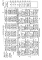
- FIG. 1 is a block diagram showing a schematic diagram of a SIMD microprocessor according to an example embodiment of this patent specification
- FIG. 2 is a detailed configuration of the SIMD microprocessor of FIG. 1 ;
- FIG. 3A is a logical configuration of identifiers of each processor element in the SIMD microprocessor of FIG. 1 ;
- FIG. 3B is a drawing showing a different logical configuration of identifiers of processor elements in the SIMD microprocessor of FIG. 1 ;
- FIG. 4A is a drawing showing a logical configuration of processor element numbers of the processor elements in the SIMD microprocessor of FIG. 1 under an operation condition;
- FIG. 4B is a drawing showing a logical configuration of the processor element numbers of the processor elements in the SIMD microprocessor of FIG. 1 under an operation condition different from the operation condition of FIG. 4A ;
- FIG. 5A is a drawing showing a logical configuration of the processor element numbers of the processor elements in the SIMD microprocessor under the operation condition of FIG. 4A ;
- FIG. 5B is a drawing showing a logical configuration of the processor element numbers of the processor elements in the SIMD microprocessor under an operation condition different from the operation condition of FIG. 5A ;
- FIG. 6A is a drawing showing a logical configuration of the processor element numbers of the processor elements in the SIMD microprocessor under the operation condition of FIG. 4A ;
- FIG. 6B is a drawing showing a logical configuration of the processor element numbers of the processor elements in the SIMD microprocessor under an operation condition different from the operation condition of FIG. 6A ;
- FIG. 7 is a detailed configuration of a SIMD microprocessor according to an example embodiment of the present patent specification.
- FIG. 8 is an example configuration of a PE number generation circuit and respective partial operations executed in the SIMD microprocessor of FIG. 7 ;
- FIG. 9 is an example configuration of a PE number generation circuit and respective partial operations executed in the SIMD microprocessor of FIG. 7 ;
- FIG. 10 is an example configuration of a PE number generation circuit and respective partial operations executed in the SIMD microprocessor of FIG. 7 ;
- FIG. 11 is a detailed configuration of an arithmetic part of the processor element included in a SIMD microprocessor according to an example embodiment of the patent specification.
- FIG. 12 is a detailed configuration of an arithmetic part of the processor element included in a SIMD microprocessor according to an example embodiment of the patent specification.
- FIG. 1 a block diagram showing a schematic diagram of a single instruction, multiple data type processor or SIMD microprocessor 2 according to an example embodiment of this patent specification is described.
- the SIMD microprocessor 2 may be included in an image processing apparatus 100 .
- the SIMD microprocessor 2 included in the image processing apparatus 100 of FIG. 1 includes, for example, a global processor 30 , a processor element group 72 , and an external interface 70 .
- the global processor 30 may be a single instruction, single data type processor or SISD processor that decodes a program to generate various control signals.
- the processor element group 72 may be a group of arrays of multiple processor elements having processors and registers as operation units.
- the processors of each processor element may reside in a processor array 62 and the registers of each processor element may reside in a register file 60 .
- the processor array 62 may perform processing according to processor element (PE) instructions.
- PE processor element
- the register file 60 may store data processed by PE instructions.
- the external interface 7 may be connected to the register file 60 .
- FIG. 2 a detailed structure of the SIMD microprocessor 2 according to an example embodiment of this patent specification is described.
- FIG. 2 mainly shows six processor elements 4 (shown as “PE” in FIG. 2 ) that are aligned in the vicinity of the center portion of the processor element group 72 .
- the part surrounded by an alternate long and short dash line and indicted with reference numeral “4” corresponds to a single processor element.
- the global processor 30 shown on the right-side part of FIG. 2 includes a program random access memory or program RAM 52 and a data random access memory or data RAM 54 as built-in memories.
- the program RAM 52 stores programs for the SIMD microprocessor 2 .
- the data RAM 54 stores operation data.
- the global processor 30 further includes, as built-in elements: a program counter 42 (shown as “PC” in FIG. 2 ) for storing a program address; general purpose registers 32 through 38 (shown as “G0”, “G1”, “G2”, and “G3” in FIG. 2 ) for storing operation data; a stack pointer 40 (shown as “SP” in FIG. 2 ) for containing an address or addresses of the data RAM to which data are saved and stored at the time of saving and restoring a register; a link register 44 (shown as “LS” in FIG. 2 ) for containing an address or addresses of the position of a call source at the time of subroutine call; an LI register 46 (shown as “LI” in FIG.
- a program counter 42 shown as “PC” in FIG. 2
- general purpose registers 32 through 38 shown as “G0”, “G1”, “G2”, and “G3” in FIG. 2
- SP stack pointer 40
- SP link register 44
- LI register 46 shown as “LI
- LN register 48 shown as “LN” in FIG. 2
- processor status register 50 shown as “P” in FIG. 2
- the instructions of the global processor 30 which may be called as the GP instructions, are executed by using these registers, an instruction decoder (not shown), an arithmetic logical unit or ALU (not shown), a memory control circuit (not shown), an interruption control unit (not shown), an external input/output or I/O control circuit (not shown), and a general purpose (GP) arithmetic control circuit (not shown).
- the global processor 30 uses the instruction decoder, a register file control circuit (not shown), and a processor element (PE) arithmetic control circuit (not shown) to control the register file 60 and the processor array 62 .
- PE processor element
- each processor element includes multiple 16-bit registers 8 and 16 that are arranged in groups corresponding to the number of processor elements, to form an array configuration.
- Each of the 16b-bit registers 8 and 16 is provided with a port for the processor array 62 .
- the processor array 62 may access the 16-bit registers 8 and 16 via a 16-bit read/write bus.
- the 16-bit read/write bus is referred to as a “register bus.”
- each processor element 4 shown in FIG. 2 includes six of the 16-bit registers 8 and 16 .
- Each of the processor elements 4 includes an arithmetic part 14 , which is surrounded by an alternate long and short dash line and indicated by reference numeral 14 in FIG. 2 .
- the arithmetic part 14 of each processor element 4 includes two sets of 16-bit ALUs 18 a and 18 b , 16-bit A registers 20 a and 20 b , and 16-bit F registers 22 a and 22 b . One set is for processing upper bit data (high order data) and the other set is for processing lower bit data (low order data).
- the arithmetic part 14 includes a lower 16-bit ALU 18 a , an upper 16-bit ALU 18 b , a lower 16-bit A register 20 a , an upper 16-bit A register 20 b , a lower 16-bit F register 22 a , and an upper 16-bit F register 22 b.
- the data read out from the register file 60 is input to one of the ALUs 18 a and 18 b and the data inside a corresponding one of the A registers 20 a and 20 b is input to the other one of the ALUs 18 a or 18 b .
- the operation results are stored in the A register 20 a and 20 b . That is, an operation process is performed with the data in the A registers 20 a and 20 b and the 16 bit-registers 8 and 16 .
- Each of the lower ALU 18 a and the upper ALU 18 b can respectively perform a 16-bit operation. Further, the lower ALU 18 a for lower bit data and the upper ALU 18 b for upper bit data are designed to cooperate with each other.
- each of the lower ALU 18 a and the upper ALU 18 b is controlled by the global processor 30 . Further, a pathway of communication may be provided between the lower ALU 18 a and the upper ALU 18 b so that the cooperative operation may be performed therebetween.
- Each of the 7 to 1 multiplexers 12 are provided for 7-to-1 selection (shown as “7 to 1 MUX” in FIG. 2 )
- Each of the 7 to 1 multiplexers 12 has a width of 16 bits and is provided at the connection part between the 16-bit registers 8 and 16 of the register file 60 and the arithmetic parts 14 of the processor array 62 .
- Each of the 7 to 1 multiplexers 12 may be connected to the register bus 10 corresponding to its own processor element 4 (local processor element) and the register buses 10 corresponding to adjacent processor elements that are aligned along the lateral direction in FIG. 2 .
- each of the 7 to 1 multiplexers 12 is connected to the register bus 10 corresponding to its own processor element (local processor element) 4 , the register buses 10 corresponding to the three processor elements 4 (the first left processor element 4 , the second left processor element 4 , and the third left processor element 4 ) aligned on its left side, and the register buses 10 for the three processor elements 4 (the first right processor element 4 , the second right processor element 4 , and the third right processor element 4 ) aligned on its right side. Accordingly, the data in the registers corresponding to the register buses 10 are selected as the target to which the operation is performed.
- the global processor 30 controls the above-described selection of the operation target.
- a shifter 16 (shown as “Shift Expand” in FIG. 2 ) is provided between the 7 to 1 multiplexer 12 and the lower and upper ALUs 18 a and 18 b .
- the shifter 16 may perform bit shift and bit expansion on the data read out from the 16 bit registers 8 and 16 .
- the global processor 30 controls the bit shift and the bit expansion of the shifter 16 .
- the two upper registers 16 included in the register file 60 are registers to which reading and writing of data from an external memory data transfer device, not shown, outside the microprocessor 2 is performed.
- the two upper registers 16 can perform reading and writing of an arbitrary 16-bit register 16 by using data buses and control signals from the external memory data transfer device outside the SIMD microprocessor 2 .
- the external memory data transfer device can access to the arbitrary 16-bit register 16 by using addresses, which is similar to making an access to a memory.
- the 16-bit registers 16 that are accessible from the external memory data transfer device are provided with respective addresses.
- the external memory data transfer device may output a control signal including an address dedicated to a 16-bit register 16 to be accessed.
- the 16-bit register 16 connected to this register bus 10 may compare its own address or local address with the address of the 16-bit register 16 to which the external memory data transfer device is making an access. When these addresses match, the 16-bit register 16 may give the external memory data transfer device an allowance of an access to the optional 16-bit register 16 .
- FIGS. 3A and 3B a logical configuration of an identifier or identifiers of each processor element in the SIMD microprocessor 2 according to the example embodiment of the present patent specification is described with reference to FIGS. 3A and 3B .
- the SIMD microprocessor 2 includes two data units of operation, each data unit being executable of 16-bit arithmetic operation. These two data units of operation may operate individually or cooperate with each other. Therefore, these data units of operation can perform the following two different operations, under control of the global processor 30 :
- Operation Condition A Execute one 32-bit arithmetic operation per processor element
- Operation Condition B Execute two 16-bit arithmetic operations at a time per processor element.
- a unique identifier is assigned to each processor element so as to designate a specific processor element.
- a data unit of operation of the processor element and an identifier assigned to the processor element may have a one-to-one relation. That is, a single processor element may have one data unit of operation with one identifier assigned thereto.
- the SIMD microprocessor 2 may execute two or more arithmetic operations in a single processor element at the same time, such as the above-described Operation Condition B. Therefore, the relation between the data unit of operation of the processor element and the identifier assigned to the processor element may not be 1:1.
- the SIMD microprocessor 2 of this example embodiment of the present patent specification may be configured to assign an identifier by each possible or executable data unit of operation in a single processor element. That is, one or more different identifiers may be assigned to corresponding one or more different data units of operation in a single processor element, depending on whether the above-described SIMD microprocessor 2 executes Operation Condition A or Operation Condition B.
- FIGS. 3A and 3B are drawings schematically showing assignments of identifiers when the SIMD microprocessor 2 is under Operation Condition A and Operation Condition B. That is, FIG. 3A is a drawing of the processor elements for Operation Condition A, where identifiers ⁇ a, b, c, . . . , l ⁇ are assigned in good order corresponding to M data units of operation included in M processor elements. “M” corresponds to any natural number greater than 1.
- FIG. 3B is a drawing of the processor elements for Operation Condition B, where identifiers ⁇ al, ah, bl, bh, cl, ch, . . . , ll, lh ⁇ are assigned in good order corresponding to M ⁇ 2 data units of operation included in M processor elements.
- FIGS. 4A , 4 B, 5 A, 5 B, 6 A, and 6 B with respect to this example embodiment show logical configurations of the identifiers (or the PE numbers) being attached to the respective processor elements 4 or respective data units of operation of each processor element 4 , with the PE numbers in ascending order, in the SIMD microprocessor 2 according to the example embodiment of the present patent specification.
- PE numbers or the identifiers for the processor elements 4 in the SIMD microprocessor 2 may also be assigned in descending order in the present patent specification.
- FIG. 4A is a drawing showing a logical configuration of the PE numbers of the processor elements 4 provided to the SIMD microprocessor 2 according to this example embodiment of the present patent specification.
- This logical configuration of the PE numbers of the processor elements 4 corresponds to the SIMD microprocessor 2 under the above-described Operation Condition A.
- the data units of operation and the processor elements 4 have a one-to-one relation, and therefore the PE numbers ⁇ 0, 1, 2, . . . M ⁇ 1 ⁇ , for example, are assigned in good order to M data units of operation of M processor elements 4 .
- “M” corresponds to any natural number greater than 1.
- FIG. 4B is a drawing showing another logical configuration of the PE numbers of the processor elements 4 provided to the SIMD microprocessor 2 according to this example embodiment of the present patent specification.
- This logical configuration of the PE numbers of the processor elements 4 corresponds to the SIMD microprocessor 2 under the above-described Operation Condition B.
- the PE numbers ⁇ 0, 1, 2, . . . , 2 ⁇ M ⁇ 1 ⁇ , for example, are assigned in good order to M ⁇ 2 data units of operation of M processor elements 4 .
- FIG. 4B for example, two PE numbers are assigned in ascending order to respective two data units of operation included in a single processing element, then the following two PE numbers are assigned in ascending order to respective two data units of operation included in a neighboring or adjacent processing element (on its right side in FIG. 4B ).
- FIG. 5A is a drawing showing a logical configuration of the PE numbers of the processor elements 4 provided to the SIMD microprocessor 2 according to this example embodiment of the present patent specification.
- This logical configuration of the PE numbers of the processor elements 4 corresponds to the SIMD microprocessor 2 under the above-described Operation Condition A.
- FIG. 5A is basically same as FIG. 4A .
- the data units of operation and the processor elements 4 have a one-to-one relation, and therefore the PE numbers ⁇ 0, 1, 2, . . . , M ⁇ 1 ⁇ , for example, are assigned in good order to M data units of operation of M processor elements 4 .
- “M” corresponds to any natural number greater than 1.
- FIG. 5B is a drawing showing yet another logical configuration of the PE numbers of the processor elements 4 provided to the SIMD microprocessor 2 according to this example embodiment of the present patent specification.
- This logical configuration of the PE numbers of the processor elements 4 corresponds to the SIMD microprocessor 2 under the above-described Operation Condition B.
- the PE numbers ⁇ 0, 1, 2, . . . , M ⁇ 1 ⁇ , for example, are assigned in good order to M ⁇ 2 data units of operation of M processor elements 4 .
- FIG. 5B is different from FIG. 4B in which an identical PE number is assigned to the data units of operation included in a same processor element in FIG. 5B while different PE numbers are assigned to the data units of operation included in an identical processor element in FIG. 4B .
- FIG. 6A is a drawing showing a logical configuration of the PE numbers of the processor elements 4 provided to the SIMD microprocessor 2 according to this example embodiment of the present patent specification.
- This logical configuration of the PE numbers of the processor elements 4 corresponds to the SIMD microprocessor 2 under the above-described Operation Condition A.
- FIG. 6A is basically same as FIG. 4A .
- the data units of operation and the processor elements 4 have a one-to-one relation, and therefore the PE numbers ⁇ 0, 1, 2, . . . , M ⁇ 1 ⁇ , for example, are assigned in good order to M data units of operation of M photoconductor elements 4 .
- “M” corresponds to any natural number greater than 1.
- FIG. 6B is a drawing showing yet another logical configuration of the PE numbers of the processor elements 4 provided to the SIMD microprocessor 2 according to this example embodiment of the present patent specification.
- This logical configuration of the PE numbers of the processor elements 4 corresponds to the SIMD microprocessor 2 under the above-described Operation Condition B.
- the PE numbers ⁇ 0, 1, 2, . . . , 2 ⁇ M ⁇ 1 ⁇ , for example, are assigned in good order to M ⁇ 2 data units of operation of M processor elements 4 .
- respective PE numbers are assigned to a first unit of two data units of operation included in each single processor element 4 through the entire processor elements 4 from the 1st processor element 4 to the Mth processor element 4 .
- respective PE numbers starting from a PE number following the last assigned PE number are assigned to the rest of the data units or second data units of the two data units of operation included in each single processor element 4 through the entire processor elements 4 . That is, a PE number immediately after the PE number assigned to the first data unit of the Mth processor element 4 may be assigned to the second data unit of the 1 st processor element 4 . More specifically, as shown in FIG.
- the PE number “PE0” may be assigned to the first data unit of operation of the 1st processor element 4
- the PE number “PE1” may be assigned to the first data unit of operation of the 2nd processor element 4
- the PE number “PE2” may be assigned to the first data unit of operation of the 3rd processor element 4
- the PE number “PE(M ⁇ 1)” may be assigned to the first data unit of operation of the Mth processor element 4 .
- PE number “PE(M)” may be assigned to the second data unit of operation of the 1st processor element 4
- the PE number “PE(M+1)” may be assigned to the second data unit of operation of the 2nd processor element 4
- the PE number “PE(M+2)” may be assigned to the second data unit of operation of the 3rd processor element 4
- the PE number “PE(2 ⁇ M ⁇ 1)” may be assigned to the second data unit of operation of the Mth processor element 4 .
- SIMD microprocessor 2 a may be provided in an image processing apparatus such as the image processing apparatus 100 .
- the SIMD microprocessor 2 a shown in FIG. 7 further includes PE number generators 66 .
- Each of the PE number generators 66 is provided to the same level of the 16-bit registers 8 and 16 included in each processor element 4 .
- the PE number generators 66 are controlled by the global processor 30 . According to the control of the global processor 30 , the PE number generators 66 may generate the PE numbers as shown in FIGS. 4A through 6B and output to the respective register buses 10 .
- the entire register buses 10 may be dedicated to the 16-bit arithmetic operations. Therefore, PE numbers from “0” to “2 16 ⁇ 1” can be generated logically.
- each of the 16-bit register bus 10 is divided into two groups of data, one of which using upper 8 bit part and the other of which using lower 8 bit part.
- the group of data using the upper 8 bit part and the group of data using the lower 8 bit part are respectively assigned to respective data units of operation included in a single processor element 4 . Therefore, PE numbers from “0” to “2 8 ⁇ 1” can be generated logically.
- the PE number generator 66 shown in FIGS. 8 through 10 includes a single 16-bit constant data K and a single multiplexer (shown as “MUX”).
- the single multiplexer may be controlled by the global processor 30 .
- the PE number generator 66 may output 16-bit constant data K to the 16-bit register bus 10 as shown in FIG. 8 .
- the PE number generator 66 may output data 2 K to a lower 8 bit part of the 16-bit register bus 10 and data 2 K+1 to an upper 8 bit part of the 16-bit register bus 10 .
- Data 2K corresponds to lower 8-bit data of values shifting the 16-bit constant data K to the left side by 1 bit
- data 2K+1 corresponds to the above-described lower 8-bit data added by data 1 that is data having the least significant bit (1 bit). This arithmetic operation is shown in FIG. 9 .
- the PE number generator 66 may output the lower 8 bits of the 16-bit constant data K to both the lower 8 bit part and the upper 8 bit part of the 16-bit register bus 10 . This arithmetic operation is shown in FIG. 10 .
- the SIMD microprocessor 2 b may be provided in an image processing apparatus such as the image processing apparatus 100 .
- the configuration of the SIMD microprocessor 2 b is substantially same as the SIMD microprocessor 2 of FIG. 2 and the SIMD microprocessor of FIG. 7 .
- Components and numbers corresponding to those of the SIMD microprocessor 2 according to the example embodiment shown in FIG. 2 are denoted by the same reference numerals and descriptions thereof are omitted or summarized.
- configurations of the SIMD microprocessor 2 b and operations that are not particularly described in this example embodiment are the same as those of the SIMD microprocessor 2 of the example embodiment previously described with reference to FIG. 2 .
- the arithmetic part 14 of the single processor element 4 shown in FIG. 11 includes a lower PE number area determination circuit 26 a , an upper PE number area determination circuit 26 b , a lower execution condition T register 24 a , and an upper execution condition T register 24 b.
- a corresponding one of the lower PE number area determination circuit 26 a and the upper PE number area determination circuit 26 b may serve as a determination unit and be provided per data unit of operation.
- the lower PE number area determination circuit 26 a may compare a lower limit PE number indicating and specifying an area that is input from the global processor 30 by an immediate data value with a PE number assigned per data unit of operation of the processor element 4 according to the above-described Operation Condition A or the above-described Operation Condition B. The result of the above-described comparison may be reflected to the lower execution condition T register 24 a .
- the lower execution condition T register 24 a may be provided per data unit of operation of each processor element for operation.
- the upper PE number area determination circuit 26 b may compare an upper limit PE number indicating and specifying an area that is input from the global processor 30 by an immediate data value with a PE number assigned per data unit of operation of the processor element 4 according to the above-described Operation Condition A or the above-described Operation Condition B. The results of the above-described comparison may be reflected to the upper execution condition T register 24 b .
- the upper execution condition T register 24 b may be provided per data unit of operation of each processor element for operation.
- the lower 16-bit ALU 18 a and the upper 16-bit ALU 18 b provided to each single processor element may determine whether the arithmetic operation is executed or not, according to the value of the lower 8-bit execution condition T register 24 a and the upper 8-bit execution condition T register 24 b , respectively. Therefore, the area to execute or not to execute the arithmetic operation can be designated at the level of each data unit of operation of the single processor element 4 .
- the single processor element 4 may include both the lower PE number area determination circuit 26 a and the upper PE number area determination circuit 26 b . In this case, however, it is only necessary that the lower PE number area determination circuit 26 a and the upper PE number area determination circuit 26 b are controlled to perform an operation identical to each other.
- FIG. 12 showing a schematic configuration of the processor element 4 according to this example embodiment of the present patent specification.
- the SIMD microprocessor 2 b with reference to FIG. 12 may be applicable for executing the operation under the above-described Operation Condition A and the above-described Operation Condition B corresponding to the logical configuration of the processor element 4 in FIGS. 4A , 4 B, 5 A, and 5 B.
- the SIMD microprocessor 2 b with reference to FIG. 12 may include an operation unit set 3 having a lower operation unit 3 a and an upper operation unit 3 b . Therefore, the SIMD microprocessor 2 b of FIG. 12 may be configured to reduce the respective sizes of the lower PE number area determination circuit 26 a and the upper PE number area determination circuit 26 b provided per data unit of operation of the processor element 4 .
- the 3rd processor element 4 may have the PE number “PE4” assigned to the lower operation unit 3 a and the PE number “PE5” assigned to the upper operation unit 3 b in FIG. 4B . That is, in FIG. 4B , the lower PE number area determination circuit 26 a may compare the lower limit PE number that is input from the global processor 30 with the constant value to determine whether or not the constant value is within the PE number area. Similarly, the upper PE number area determination circuit 26 b may compare the upper limit PE number that is input from the global processor 30 with the constant value to determine whether or not the constant value is within the PE number area.
- the constant values may be provided corresponding to the PE number of FIG. 4B . That is, when the processor element 4 shown in FIG. 12 has the PE number “PE2” same as the condition corresponding to the logical configuration of the processor elements 4 in FIG. 4A or FIG. 5A , for example, the PE number “PE4” may be assigned to the constant value of the lower PE number area determination circuit 26 a associated with the lower ALU 18 a and the PE number “PE5” may be assigned to the constant value of the upper PE number area determination circuit 26 b associated with the upper ALU 18 b.
- the SIMD microprocessor 2 b may be applicable to the condition corresponding to the logical configuration of the processor elements 4 in FIG. 4B .
- the upper limit PE number and the lower limit PE number that are input from the global processor 30 may be multiplied by two to be provided to the lower PE number area determination circuit 26 a and the upper PE number area determination circuit 26 b , respectively.
- the upper PE number area determination circuit 26 b associated with the upper ALU 18 b may be configured not to compare the least significant bit (1 bit). That is, the upper PE number area determination circuit 26 b may ignore the comparison result of the least significant bit (1 bit).
- both the lower PE number area determination circuit 26 a associated with the lower ALU 18 a and the upper PE number area determination circuit 26 b associated with the upper ALU 18 b may determine whether the constant value “4” is substantially provided within a selection area by data from the global processor 30 .
- both the lower PE number area determination circuit 26 a and the upper PE number area determination circuit 26 b may use a value obtained by multiplying the actual PE number “2” by two under the condition of the logical configurations in FIG. 4A or FIG. 5A . Accordingly, the upper limit PE number and the lower limit PE number that are input from the global processor 30 may also apply a value multiplied by two.
- PE2 the PE number “PE2”
- PE2 the PE number “PE2”
- This invention may be conveniently implemented using a conventional general-purpose digital computer programmed according to the teachings of the present specification, as will be apparent to those skilled in the computer arts.
- Appropriate software coding can readily be prepared by skilled programmers based on the teachings of the present disclosure, as will be apparent to those skilled in the software arts.
- the present invention may also be implemented by the preparation of application-specific integrated circuits or by interconnecting an appropriate network of conventional component circuits, as will be readily apparent to those skilled in the art.
Abstract
Description
Claims (16)
Applications Claiming Priority (2)
| Application Number | Priority Date | Filing Date | Title |
|---|---|---|---|
| JP2007049387A JP4801605B2 (en) | 2007-02-28 | 2007-02-28 | SIMD type microprocessor |
| JP2007-049387 | 2007-02-28 |
Publications (2)
| Publication Number | Publication Date |
|---|---|
| US20080209165A1 US20080209165A1 (en) | 2008-08-28 |
| US8060726B2 true US8060726B2 (en) | 2011-11-15 |
Family
ID=39717260
Family Applications (1)
| Application Number | Title | Priority Date | Filing Date |
|---|---|---|---|
| US12/038,518 Expired - Fee Related US8060726B2 (en) | 2007-02-28 | 2008-02-27 | SIMD microprocessor, image processing apparatus including same, and image processing method used therein |
Country Status (2)
| Country | Link |
|---|---|
| US (1) | US8060726B2 (en) |
| JP (1) | JP4801605B2 (en) |
Families Citing this family (7)
| Publication number | Priority date | Publication date | Assignee | Title |
|---|---|---|---|---|
| JP5049802B2 (en) | 2008-01-22 | 2012-10-17 | 株式会社リコー | Image processing device |
| JP2010122741A (en) * | 2008-11-17 | 2010-06-03 | Kumamoto Univ | Data processor |
| JP5760532B2 (en) * | 2011-03-14 | 2015-08-12 | 株式会社リコー | PROCESSOR DEVICE AND ITS OPERATION METHOD |
| JP5829331B2 (en) * | 2011-09-27 | 2015-12-09 | ルネサスエレクトロニクス株式会社 | Apparatus for simultaneously transferring data in a plurality of target areas (ROI) in a SIMD processor system in parallel |
| JP2014016894A (en) * | 2012-07-10 | 2014-01-30 | Renesas Electronics Corp | Parallel arithmetic device, data processing system with parallel arithmetic device, and data processing program |
| US10754818B2 (en) | 2014-08-12 | 2020-08-25 | ArchiTek Corporation | Multiprocessor device for executing vector processing commands |
| US11106268B2 (en) * | 2018-07-29 | 2021-08-31 | Redpine Signals, Inc. | Method and system for saving power in a real time hardware processing unit |
Citations (8)
| Publication number | Priority date | Publication date | Assignee | Title |
|---|---|---|---|---|
| US4748585A (en) * | 1985-12-26 | 1988-05-31 | Chiarulli Donald M | Processor utilizing reconfigurable process segments to accomodate data word length |
| US5410727A (en) * | 1989-10-24 | 1995-04-25 | International Business Machines Corporation | Input/output system for a massively parallel, single instruction, multiple data (SIMD) computer providing for the simultaneous transfer of data between a host computer input/output system and all SIMD memory devices |
| US5590356A (en) * | 1994-08-23 | 1996-12-31 | Massachusetts Institute Of Technology | Mesh parallel computer architecture apparatus and associated methods |
| JP2002007359A (en) | 2000-06-21 | 2002-01-11 | Sony Corp | Method and device for parallel processing simd control |
| JP2002091929A (en) | 2000-09-11 | 2002-03-29 | Matsushita Electric Ind Co Ltd | Simd type parallel processor |
| US20030151608A1 (en) * | 2002-01-17 | 2003-08-14 | Chung Chris Yoochang | Programmable 3D graphics pipeline for multimedia applications |
| JP2006260479A (en) | 2005-03-18 | 2006-09-28 | Ricoh Co Ltd | Simd type microprocessor and data processing method |
| JP2007034473A (en) | 2005-07-25 | 2007-02-08 | Ricoh Co Ltd | Data processing method in simd type microprocessor |
-
2007
- 2007-02-28 JP JP2007049387A patent/JP4801605B2/en not_active Expired - Fee Related
-
2008
- 2008-02-27 US US12/038,518 patent/US8060726B2/en not_active Expired - Fee Related
Patent Citations (8)
| Publication number | Priority date | Publication date | Assignee | Title |
|---|---|---|---|---|
| US4748585A (en) * | 1985-12-26 | 1988-05-31 | Chiarulli Donald M | Processor utilizing reconfigurable process segments to accomodate data word length |
| US5410727A (en) * | 1989-10-24 | 1995-04-25 | International Business Machines Corporation | Input/output system for a massively parallel, single instruction, multiple data (SIMD) computer providing for the simultaneous transfer of data between a host computer input/output system and all SIMD memory devices |
| US5590356A (en) * | 1994-08-23 | 1996-12-31 | Massachusetts Institute Of Technology | Mesh parallel computer architecture apparatus and associated methods |
| JP2002007359A (en) | 2000-06-21 | 2002-01-11 | Sony Corp | Method and device for parallel processing simd control |
| JP2002091929A (en) | 2000-09-11 | 2002-03-29 | Matsushita Electric Ind Co Ltd | Simd type parallel processor |
| US20030151608A1 (en) * | 2002-01-17 | 2003-08-14 | Chung Chris Yoochang | Programmable 3D graphics pipeline for multimedia applications |
| JP2006260479A (en) | 2005-03-18 | 2006-09-28 | Ricoh Co Ltd | Simd type microprocessor and data processing method |
| JP2007034473A (en) | 2005-07-25 | 2007-02-08 | Ricoh Co Ltd | Data processing method in simd type microprocessor |
Also Published As
| Publication number | Publication date |
|---|---|
| JP2008217061A (en) | 2008-09-18 |
| US20080209165A1 (en) | 2008-08-28 |
| JP4801605B2 (en) | 2011-10-26 |
Similar Documents
| Publication | Publication Date | Title |
|---|---|---|
| US8060726B2 (en) | SIMD microprocessor, image processing apparatus including same, and image processing method used therein | |
| US5606520A (en) | Address generator with controllable modulo power of two addressing capability | |
| US6070003A (en) | System and method of memory access in apparatus having plural processors and plural memories | |
| JP4156794B2 (en) | Method and apparatus for efficient synchronous MIMD operation using iVLIW inter-PE communication | |
| US5371896A (en) | Multi-processor having control over synchronization of processors in mind mode and method of operation | |
| US5522083A (en) | Reconfigurable multi-processor operating in SIMD mode with one processor fetching instructions for use by remaining processors | |
| US20080072011A1 (en) | SIMD type microprocessor | |
| EP2372530A1 (en) | Data processing method and device | |
| EP1333381A2 (en) | System and method for processing image, and compiler for use in this system | |
| JPH0769818B2 (en) | Data processing device | |
| US10908916B2 (en) | Apparatus and method for executing a plurality of threads | |
| JP6967597B2 (en) | An image processor with a configurable number of active cores and an internal network that supports it | |
| US20060236075A1 (en) | SIMD microprocessor and data processing method | |
| JP3971535B2 (en) | SIMD type processor | |
| US5034879A (en) | Programmable data path width in a programmable unit having plural levels of subinstruction sets | |
| US4975837A (en) | Programmable unit having plural levels of subinstruction sets where a portion of the lower level is embedded in the code stream of the upper level of the subinstruction sets | |
| JPH0461390B2 (en) | ||
| US20020138535A1 (en) | SIMD sum of product arithmetic method and circuit, and semiconductor integrated circuit device equipped with the SIMD sum of product arithmetic circuit | |
| CN112463218B (en) | Instruction emission control method and circuit, data processing method and circuit | |
| EP0177268B1 (en) | Programmable data path width in a programmable unit having plural levels of subinstructions sets | |
| JP4482356B2 (en) | Image processing method and image processing apparatus using SIMD processor | |
| US8024550B2 (en) | SIMD processor with each processing element receiving buffered control signal from clocked register positioned in the middle of the group | |
| JP5369669B2 (en) | SIMD type microprocessor | |
| US5473774A (en) | Method for conflict detection in parallel processing system | |
| JP3971543B2 (en) | SIMD type processor |
Legal Events
| Date | Code | Title | Description |
|---|---|---|---|
| AS | Assignment |
Owner name: RICOH COMPANY, LTD,JAPAN Free format text: ASSIGNMENT OF ASSIGNORS INTEREST;ASSIGNOR:OZAKI, TOMOAKI;REEL/FRAME:020572/0339 Effective date: 20080226 Owner name: RICOH COMPANY, LTD, JAPAN Free format text: ASSIGNMENT OF ASSIGNORS INTEREST;ASSIGNOR:OZAKI, TOMOAKI;REEL/FRAME:020572/0339 Effective date: 20080226 |
|
| FEPP | Fee payment procedure |
Free format text: PAYOR NUMBER ASSIGNED (ORIGINAL EVENT CODE: ASPN); ENTITY STATUS OF PATENT OWNER: LARGE ENTITY |
|
| STCF | Information on status: patent grant |
Free format text: PATENTED CASE |
|
| FPAY | Fee payment |
Year of fee payment: 4 |
|
| FEPP | Fee payment procedure |
Free format text: MAINTENANCE FEE REMINDER MAILED (ORIGINAL EVENT CODE: REM.); ENTITY STATUS OF PATENT OWNER: LARGE ENTITY |
|
| LAPS | Lapse for failure to pay maintenance fees |
Free format text: PATENT EXPIRED FOR FAILURE TO PAY MAINTENANCE FEES (ORIGINAL EVENT CODE: EXP.); ENTITY STATUS OF PATENT OWNER: LARGE ENTITY |
|
| STCH | Information on status: patent discontinuation |
Free format text: PATENT EXPIRED DUE TO NONPAYMENT OF MAINTENANCE FEES UNDER 37 CFR 1.362 |
|
| FP | Lapsed due to failure to pay maintenance fee |
Effective date: 20191115 |