US8062771B2 - Ambipolar host in organic light emitting diode - Google Patents
Ambipolar host in organic light emitting diode Download PDFInfo
- Publication number
- US8062771B2 US8062771B2 US12/694,939 US69493910A US8062771B2 US 8062771 B2 US8062771 B2 US 8062771B2 US 69493910 A US69493910 A US 69493910A US 8062771 B2 US8062771 B2 US 8062771B2
- Authority
- US
- United States
- Prior art keywords
- optionally substituted
- bis
- iridium
- iii
- emitting component
- Prior art date
- Legal status (The legal status is an assumption and is not a legal conclusion. Google has not performed a legal analysis and makes no representation as to the accuracy of the status listed.)
- Active, expires
Links
- 0 *C1=NC([5*])=C(C2=C([4*])N=C([3*])C([2*])C2[1*])C([8*])C1[7*] Chemical compound *C1=NC([5*])=C(C2=C([4*])N=C([3*])C([2*])C2[1*])C([8*])C1[7*] 0.000 description 19
- KHBJKNYCHPVRBH-UHFFFAOYSA-N C1=CC2=C(C=C1)N(C1=CN=CC(C3=CC(N4C5=C(C=CC=C5)C5=C4/C=C\C=C/5)=CN=C3)=C1)C1=C2C=CC=C1.C1=CC=C(N(C2=CC=CC=C2)C2=CC=C(C3=CN=CC(C4=CC(C5=CC=C(N(C6=CC=CC=C6)C6=CC=CC=C6)C=C5)=CN=C4)=C3)C=C2)C=C1.C1=CC=C(N(C2=CC=CC=C2)C2=CC=CC(C3=CN=CC(C4=CC(C5=CC(N(C6=CC=CC=C6)C6=CC=CC=C6)=CC=C5)=CN=C4)=C3)=C2)C=C1.C1=CC=C(N(C2=CC=CC=C2)C2=CN=CC(C3=CC(N(C4=CC=CC=C4)C4=CC=CC=C4)=CN=C3)=C2)C=C1.C1=CC=C2C(=C1)C1=C(C=CC=C1)N2C1=CC=C(C2=CN=CC(C3=CC(C4=CC=C(N5C6=CC=CC=C6C6=C5C=CC=C6)C=C4)=CN=C3)=C2)C=C1.C1=CC=C2C(=C1)C1=C(C=CC=C1)N2C1=CC=CC(C2=CN=CC(C3=CC(C4=CC(N5C6=CC=CC=C6C6=C5C=CC=C6)=CC=C4)=CN=C3)=C2)=C1.CC1=CC=C(N(C2=CC=C(C)C=C2)C2=CC=C(C3=CN=CC(C4=CC(C5=CC=C(N(C6=CC=C(C)C=C6)C6=CC=C(C)C=C6)C=C5)=CN=C4)=C3)C=C2)C=C1.CC1=CC=C2C(=C1)C1=C(C=CC(C)=C1)N2C1=CC=C(C2=CN=CC(C3=CC(C4=CC=C(N5C6=CC=C(C)C=C6C6=C5C=CC(C)=C6)C=C4)=CN=C3)=C2)C=C1 Chemical compound C1=CC2=C(C=C1)N(C1=CN=CC(C3=CC(N4C5=C(C=CC=C5)C5=C4/C=C\C=C/5)=CN=C3)=C1)C1=C2C=CC=C1.C1=CC=C(N(C2=CC=CC=C2)C2=CC=C(C3=CN=CC(C4=CC(C5=CC=C(N(C6=CC=CC=C6)C6=CC=CC=C6)C=C5)=CN=C4)=C3)C=C2)C=C1.C1=CC=C(N(C2=CC=CC=C2)C2=CC=CC(C3=CN=CC(C4=CC(C5=CC(N(C6=CC=CC=C6)C6=CC=CC=C6)=CC=C5)=CN=C4)=C3)=C2)C=C1.C1=CC=C(N(C2=CC=CC=C2)C2=CN=CC(C3=CC(N(C4=CC=CC=C4)C4=CC=CC=C4)=CN=C3)=C2)C=C1.C1=CC=C2C(=C1)C1=C(C=CC=C1)N2C1=CC=C(C2=CN=CC(C3=CC(C4=CC=C(N5C6=CC=CC=C6C6=C5C=CC=C6)C=C4)=CN=C3)=C2)C=C1.C1=CC=C2C(=C1)C1=C(C=CC=C1)N2C1=CC=CC(C2=CN=CC(C3=CC(C4=CC(N5C6=CC=CC=C6C6=C5C=CC=C6)=CC=C4)=CN=C3)=C2)=C1.CC1=CC=C(N(C2=CC=C(C)C=C2)C2=CC=C(C3=CN=CC(C4=CC(C5=CC=C(N(C6=CC=C(C)C=C6)C6=CC=C(C)C=C6)C=C5)=CN=C4)=C3)C=C2)C=C1.CC1=CC=C2C(=C1)C1=C(C=CC(C)=C1)N2C1=CC=C(C2=CN=CC(C3=CC(C4=CC=C(N5C6=CC=C(C)C=C6C6=C5C=CC(C)=C6)C=C4)=CN=C3)=C2)C=C1 KHBJKNYCHPVRBH-UHFFFAOYSA-N 0.000 description 2
- LRSVRPZJSKWFAP-UHFFFAOYSA-N BrC1=CC(N2C3=C(C=CC=C3)C3=C2/C=C\C=C/3)=CN=C1.BrC1=CN=CC(Br)=C1.C1=CC2=C(C=C1)C1=C(/C=C\C=C/1)N2.C1=CC2=C(C=C1)N(C1=CN=CC(C3=CC(N4C5=C(C=CC=C5)C5=C4/C=C\C=C/5)=CN=C3)=C1)C1=C2C=CC=C1.CC1(C)OB(B2OC(C)(C)C(C)(C)O2)OC1(C)C Chemical compound BrC1=CC(N2C3=C(C=CC=C3)C3=C2/C=C\C=C/3)=CN=C1.BrC1=CN=CC(Br)=C1.C1=CC2=C(C=C1)C1=C(/C=C\C=C/1)N2.C1=CC2=C(C=C1)N(C1=CN=CC(C3=CC(N4C5=C(C=CC=C5)C5=C4/C=C\C=C/5)=CN=C3)=C1)C1=C2C=CC=C1.CC1(C)OB(B2OC(C)(C)C(C)(C)O2)OC1(C)C LRSVRPZJSKWFAP-UHFFFAOYSA-N 0.000 description 1
- SKODVKMYBGXHOZ-UHFFFAOYSA-N C1=C/C2=C/C=C3/C=CC(C4=CC=C(N(C5=CC=C(C6=C7C=CC8=CC=C/C9=C/C=C(/C=C6)C7=C89)C=C5)C5=CC=C(C6=C7C=CC8=CC=C/C9=C/C=C(/C=C6)C7=C89)C=C5)C=C4)=C4C=CC(=C1)C2=C43 Chemical compound C1=C/C2=C/C=C3/C=CC(C4=CC=C(N(C5=CC=C(C6=C7C=CC8=CC=C/C9=C/C=C(/C=C6)C7=C89)C=C5)C5=CC=C(C6=C7C=CC8=CC=C/C9=C/C=C(/C=C6)C7=C89)C=C5)C=C4)=C4C=CC(=C1)C2=C43 SKODVKMYBGXHOZ-UHFFFAOYSA-N 0.000 description 1
- MMDHRNBUPKQVQE-XWJZPQAGSA-L C1=C/C2=C/C=C3/C=CC(C4=CC=C(N(C5=CC=C(C6=C7C=CC8=CC=C/C9=C/C=C(/C=C6)C7=C89)C=C5)C5=CC=C(C6=C7\C=C/C8=C/C=C\C9=CC=C(\C=C/6)C7=C98)C=C5)C=C4)=C4C=CC(=C1)C2=C43.CC(C)(C)C1=CC(CCC2=CC=C(N3C4=C(C=CC=C4)C4=C3C=CC=C4)C=C2)=O[Pt@@]2(O1)C1=CC(F)=CC(F)=C1C1=N2C=C(CCC2=CC=C(N3C4=C(C=CC=C4)C4=C3C=CC=C4)C=C2)C=C1.CC1=CC(CCC2=CC=C(N3C4=C(C=CC=C4)C4=C3C=CC=C4)C=C2)=O[Pt@@]2(O1)C1=CC(F)=CC(F)=C1C1=N2C=CC=C1.FC1=CC(F)=C2C3=CC=CC=N3[Ir]3(C2=C1)C1=C(C=CC=C1)C1=CC=C2C=CC=CC2=N13.OC1=CC=CC=C1C1=NC(C2=CC=CC=C2)=C(C2=CC=CC=C2)N1C1=CC=C(OC2=CC=C(N3C(C4=CC5=C(C=CC=C5)C=C4O)=NC(C4=CC=CC=C4)=C3C3=CC=CC=C3)C=C2)C=C1.OC1=CC=CC=C1C1=NC(C2=CC=CC=C2)=C(C2=CC=CC=C2)N1C1=CC=C(OC2=CC=C(N3C(C4=CC5=C(C=CC=C5)C=C4O)=NC4=C3C3=C(C=CC=C3)C3=CC=CC=C34)C=C2)C=C1 Chemical compound C1=C/C2=C/C=C3/C=CC(C4=CC=C(N(C5=CC=C(C6=C7C=CC8=CC=C/C9=C/C=C(/C=C6)C7=C89)C=C5)C5=CC=C(C6=C7\C=C/C8=C/C=C\C9=CC=C(\C=C/6)C7=C98)C=C5)C=C4)=C4C=CC(=C1)C2=C43.CC(C)(C)C1=CC(CCC2=CC=C(N3C4=C(C=CC=C4)C4=C3C=CC=C4)C=C2)=O[Pt@@]2(O1)C1=CC(F)=CC(F)=C1C1=N2C=C(CCC2=CC=C(N3C4=C(C=CC=C4)C4=C3C=CC=C4)C=C2)C=C1.CC1=CC(CCC2=CC=C(N3C4=C(C=CC=C4)C4=C3C=CC=C4)C=C2)=O[Pt@@]2(O1)C1=CC(F)=CC(F)=C1C1=N2C=CC=C1.FC1=CC(F)=C2C3=CC=CC=N3[Ir]3(C2=C1)C1=C(C=CC=C1)C1=CC=C2C=CC=CC2=N13.OC1=CC=CC=C1C1=NC(C2=CC=CC=C2)=C(C2=CC=CC=C2)N1C1=CC=C(OC2=CC=C(N3C(C4=CC5=C(C=CC=C5)C=C4O)=NC(C4=CC=CC=C4)=C3C3=CC=CC=C3)C=C2)C=C1.OC1=CC=CC=C1C1=NC(C2=CC=CC=C2)=C(C2=CC=CC=C2)N1C1=CC=C(OC2=CC=C(N3C(C4=CC5=C(C=CC=C5)C=C4O)=NC4=C3C3=C(C=CC=C3)C3=CC=CC=C34)C=C2)C=C1 MMDHRNBUPKQVQE-XWJZPQAGSA-L 0.000 description 1
- YOQJYPILFBOFOK-UHFFFAOYSA-N C1=CC2=C(C=C1)C1=N(/C=C\2)[Ir]C2=C1SC=C2.C1=CC=C2C(=C1)[Ir]N1=C2C2=C(C=CC=C2)C=C1.C1=CC=N2[Ir]C3=C(SC4=C3C=CC=C4)C2=C1.CC1(C)C2=C(C=CC=C2)C2=C1C=C1C(=C2)[Ir]N2=CC(C3=C/C4=C(\C=C/3)C3=CC=CC=C3C4(C)C)=CC=C12.F.F.F.PP(P)[Ir] Chemical compound C1=CC2=C(C=C1)C1=N(/C=C\2)[Ir]C2=C1SC=C2.C1=CC=C2C(=C1)[Ir]N1=C2C2=C(C=CC=C2)C=C1.C1=CC=N2[Ir]C3=C(SC4=C3C=CC=C4)C2=C1.CC1(C)C2=C(C=CC=C2)C2=C1C=C1C(=C2)[Ir]N2=CC(C3=C/C4=C(\C=C/3)C3=CC=CC=C3C4(C)C)=CC=C12.F.F.F.PP(P)[Ir] YOQJYPILFBOFOK-UHFFFAOYSA-N 0.000 description 1
- BDNOWOOVLCVKAN-UHFFFAOYSA-N C1=CC2=C(C=C1)N(C1=CC=C(C3=CC=C(N4C5=C(C=CC=C5)C5=C4C=CC=C5)N=C3)C=N1)C1=C2C=CC=C1.C1=CC=C(N(C2=CC=CC=C2)C2=CC=C(C3=CC=C(N(C4=CC=CC=C4)C4=CC=CC=C4)N=C3)C=N2)C=C1.C1=CC=C(N(C2=CC=CC=C2)C2=CC=CC=C2)C=C1.C1=CC=C(N(C2=CC=CC=C2)C2=CN=CC(C3=CC(N(C4=CC=CC=C4)C4=CC=CC=C4)=CN=C3)=C2)C=C1.C1=CC=C(N2C3=C(C=CC=C3)C3=C2C=CC=C3)C=C1.CC(C)C.CC(C)C.CC(C)C1=CC=C(C(C)C)C=C1.CC(C)C1=CC=CC(C(C)C)=C1.CC(C)N(C1=CC=CC=C1)C1=CC=CC=C1.CC(C)N1C2=C(C=CC=C2)C2=C/C=C/C=C\21 Chemical compound C1=CC2=C(C=C1)N(C1=CC=C(C3=CC=C(N4C5=C(C=CC=C5)C5=C4C=CC=C5)N=C3)C=N1)C1=C2C=CC=C1.C1=CC=C(N(C2=CC=CC=C2)C2=CC=C(C3=CC=C(N(C4=CC=CC=C4)C4=CC=CC=C4)N=C3)C=N2)C=C1.C1=CC=C(N(C2=CC=CC=C2)C2=CC=CC=C2)C=C1.C1=CC=C(N(C2=CC=CC=C2)C2=CN=CC(C3=CC(N(C4=CC=CC=C4)C4=CC=CC=C4)=CN=C3)=C2)C=C1.C1=CC=C(N2C3=C(C=CC=C3)C3=C2C=CC=C3)C=C1.CC(C)C.CC(C)C.CC(C)C1=CC=C(C(C)C)C=C1.CC(C)C1=CC=CC(C(C)C)=C1.CC(C)N(C1=CC=CC=C1)C1=CC=CC=C1.CC(C)N1C2=C(C=CC=C2)C2=C/C=C/C=C\21 BDNOWOOVLCVKAN-UHFFFAOYSA-N 0.000 description 1
- HPKMJJAJGFCCRD-UHFFFAOYSA-N C1=CC2=C(C=C1)N(C1=CC=C(C3=CN=CC(C4=CC(C5=CC=C(N6C7=C(C=CC=C7)C7=C6C=CC=C7)C=C5)=CN=C4)=C3)C=C1)C1=C2C=CC=C1.C1=CC2=C(C=C1)N(C1=CN=CC(C3=CC(N4C5=C(C=CC=C5)C5=C4C=CC=C5)=CN=C3)=C1)C1=C2C=CC=C1.C1=CC=C(N(C2=CC=CC=C2)C2=CC=C(C3=CN=CC(C4=CC(C5=CC=C(N(C6=CC=CC=C6)C6=CC=CC=C6)C=C5)=CN=C4)=C3)C=C2)C=C1.CC1=CC2=C(C=C1)N(C1=CC=C(C3=CN=CC(C4=CC(C5=CC=C(N6C7=C(C=C(C)C=C7)C7=C6C=CC(C)=C7)C=C5)=CN=C4)=C3)C=C1)C1=C2C=C(C)C=C1.CC1=CC=C(N(C2=CC=C(C)C=C2)C2=CC=C(C3=CN=CC(C4=CC(C5=CC=C(N(C6=CC=C(C)C=C6)C6=CC=C(C)C=C6)C=C5)=CN=C4)=C3)C=C2)C=C1 Chemical compound C1=CC2=C(C=C1)N(C1=CC=C(C3=CN=CC(C4=CC(C5=CC=C(N6C7=C(C=CC=C7)C7=C6C=CC=C7)C=C5)=CN=C4)=C3)C=C1)C1=C2C=CC=C1.C1=CC2=C(C=C1)N(C1=CN=CC(C3=CC(N4C5=C(C=CC=C5)C5=C4C=CC=C5)=CN=C3)=C1)C1=C2C=CC=C1.C1=CC=C(N(C2=CC=CC=C2)C2=CC=C(C3=CN=CC(C4=CC(C5=CC=C(N(C6=CC=CC=C6)C6=CC=CC=C6)C=C5)=CN=C4)=C3)C=C2)C=C1.CC1=CC2=C(C=C1)N(C1=CC=C(C3=CN=CC(C4=CC(C5=CC=C(N6C7=C(C=C(C)C=C7)C7=C6C=CC(C)=C7)C=C5)=CN=C4)=C3)C=C1)C1=C2C=C(C)C=C1.CC1=CC=C(N(C2=CC=C(C)C=C2)C2=CC=C(C3=CN=CC(C4=CC(C5=CC=C(N(C6=CC=C(C)C=C6)C6=CC=C(C)C=C6)C=C5)=CN=C4)=C3)C=C2)C=C1 HPKMJJAJGFCCRD-UHFFFAOYSA-N 0.000 description 1
- OGNLGBINRHXCGT-UHFFFAOYSA-N C1=CC2=C(C=C1)N(C1=CN=CC(C3=CC(N4C5=C(C=CC=C5)C5=C4C=CC=C5)=CN=C3)=C1)C1=C2C=CC=C1 Chemical compound C1=CC2=C(C=C1)N(C1=CN=CC(C3=CC(N4C5=C(C=CC=C5)C5=C4C=CC=C5)=CN=C3)=C1)C1=C2C=CC=C1 OGNLGBINRHXCGT-UHFFFAOYSA-N 0.000 description 1
- LJFMCTDFQKYAAH-UHFFFAOYSA-N C1=CC=C(N(C2=CC=CC=C2)C2=CC(C3=CN=CC(C4=CC(C5=CC=CC(N(C6=CC=CC=C6)C6=CC=CC=C6)=C5)=CN=C4)=C3)=CC=C2)C=C1.C1=CC=C(N(C2=CC=CC=C2)C2=CC=C(C3=CC=C(C4=CC=C(C5=CC=C(N(C6=CC=CC=C6)C6=CC=CC=C6)C=C5)N=C4)C=N3)C=C2)C=C1.C1=CC=C2C(=C1)C1=C(C=CC=C1)N2C1=CC=C(C2=CC=C(C3=CC=C(C4=CC=C(N5C6=CC=CC=C6C6=C5C=CC=C6)C=C4)N=C3)C=N2)C=C1.C1=CC=C2C(=C1)C1=C(C=CC=C1)N2C1=CC=CC(C2=CN=CC(C3=CC(C4=CC(N5C6=CC=CC=C6C6=C5C=CC=C6)=CC=C4)=CN=C3)=C2)=C1 Chemical compound C1=CC=C(N(C2=CC=CC=C2)C2=CC(C3=CN=CC(C4=CC(C5=CC=CC(N(C6=CC=CC=C6)C6=CC=CC=C6)=C5)=CN=C4)=C3)=CC=C2)C=C1.C1=CC=C(N(C2=CC=CC=C2)C2=CC=C(C3=CC=C(C4=CC=C(C5=CC=C(N(C6=CC=CC=C6)C6=CC=CC=C6)C=C5)N=C4)C=N3)C=C2)C=C1.C1=CC=C2C(=C1)C1=C(C=CC=C1)N2C1=CC=C(C2=CC=C(C3=CC=C(C4=CC=C(N5C6=CC=CC=C6C6=C5C=CC=C6)C=C4)N=C3)C=N2)C=C1.C1=CC=C2C(=C1)C1=C(C=CC=C1)N2C1=CC=CC(C2=CN=CC(C3=CC(C4=CC(N5C6=CC=CC=C6C6=C5C=CC=C6)=CC=C4)=CN=C3)=C2)=C1 LJFMCTDFQKYAAH-UHFFFAOYSA-N 0.000 description 1
- VFHYCBVXDMZBBM-UHFFFAOYSA-N CC1(C)C2=C(C=CC=C2)C2=C1/C=C1/C3=N(/C=C\C4=C3C=CC=C4)[Ir]/C1=C/2 Chemical compound CC1(C)C2=C(C=CC=C2)C2=C1/C=C1/C3=N(/C=C\C4=C3C=CC=C4)[Ir]/C1=C/2 VFHYCBVXDMZBBM-UHFFFAOYSA-N 0.000 description 1
- YXKHVVAZNPPWCN-UHFFFAOYSA-N CC1=CC2=C(C=CC=C2)C=C1C1=NC(C2=CC=CC=C2)=C(C2=CC=CC=C2)N1C1=CC=C(OC2=CC=C(N3C(C4=CC=CC=C4O)=NC(C4=CC=CC=C4)=C3C3=CC=CC=C3)C=C2)C=C1.CC1=CC2=C(C=CC=C2)C=C1C1C/C2=C(/C3=C(C=CC=C3)C3=CC=CC=C32)N1C1=CC=C(OC2=CC=C(N3C(C4=CC=CC=C4O)=NC(C4=CC=CC=C4)=C3C3=CC=CC=C3)C=C2)C=C1 Chemical compound CC1=CC2=C(C=CC=C2)C=C1C1=NC(C2=CC=CC=C2)=C(C2=CC=CC=C2)N1C1=CC=C(OC2=CC=C(N3C(C4=CC=CC=C4O)=NC(C4=CC=CC=C4)=C3C3=CC=CC=C3)C=C2)C=C1.CC1=CC2=C(C=CC=C2)C=C1C1C/C2=C(/C3=C(C=CC=C3)C3=CC=CC=C32)N1C1=CC=C(OC2=CC=C(N3C(C4=CC=CC=C4O)=NC(C4=CC=CC=C4)=C3C3=CC=CC=C3)C=C2)C=C1 YXKHVVAZNPPWCN-UHFFFAOYSA-N 0.000 description 1
- OXHBKGURKPVEIE-UHFFFAOYSA-N FC1=CC(F)=C2C(=C1)[Ir]1(N3=CC=CN3B(N3C=CC=N3)(N3C=CC=N3)N3C=CC=N31)N1=C2C=CC=C1 Chemical compound FC1=CC(F)=C2C(=C1)[Ir]1(N3=CC=CN3B(N3C=CC=N3)(N3C=CC=N3)N3C=CC=N31)N1=C2C=CC=C1 OXHBKGURKPVEIE-UHFFFAOYSA-N 0.000 description 1
- ZDFXGEMIUWGLIO-UHFFFAOYSA-N FC1=CC(F)=C2C3=CC=CC=N3[Ir]3(C4=CC=CC=C4C4=CC=C5C=CC=CC5=N43)C2=C1 Chemical compound FC1=CC(F)=C2C3=CC=CC=N3[Ir]3(C4=CC=CC=C4C4=CC=C5C=CC=CC5=N43)C2=C1 ZDFXGEMIUWGLIO-UHFFFAOYSA-N 0.000 description 1
Images


Classifications
-
- C—CHEMISTRY; METALLURGY
- C07—ORGANIC CHEMISTRY
- C07D—HETEROCYCLIC COMPOUNDS
- C07D401/00—Heterocyclic compounds containing two or more hetero rings, having nitrogen atoms as the only ring hetero atoms, at least one ring being a six-membered ring with only one nitrogen atom
- C07D401/14—Heterocyclic compounds containing two or more hetero rings, having nitrogen atoms as the only ring hetero atoms, at least one ring being a six-membered ring with only one nitrogen atom containing three or more hetero rings
-
- C—CHEMISTRY; METALLURGY
- C07—ORGANIC CHEMISTRY
- C07D—HETEROCYCLIC COMPOUNDS
- C07D213/00—Heterocyclic compounds containing six-membered rings, not condensed with other rings, with one nitrogen atom as the only ring hetero atom and three or more double bonds between ring members or between ring members and non-ring members
- C07D213/02—Heterocyclic compounds containing six-membered rings, not condensed with other rings, with one nitrogen atom as the only ring hetero atom and three or more double bonds between ring members or between ring members and non-ring members having three double bonds between ring members or between ring members and non-ring members
- C07D213/04—Heterocyclic compounds containing six-membered rings, not condensed with other rings, with one nitrogen atom as the only ring hetero atom and three or more double bonds between ring members or between ring members and non-ring members having three double bonds between ring members or between ring members and non-ring members having no bond between the ring nitrogen atom and a non-ring member or having only hydrogen or carbon atoms directly attached to the ring nitrogen atom
- C07D213/24—Heterocyclic compounds containing six-membered rings, not condensed with other rings, with one nitrogen atom as the only ring hetero atom and three or more double bonds between ring members or between ring members and non-ring members having three double bonds between ring members or between ring members and non-ring members having no bond between the ring nitrogen atom and a non-ring member or having only hydrogen or carbon atoms directly attached to the ring nitrogen atom with substituted hydrocarbon radicals attached to ring carbon atoms
- C07D213/36—Radicals substituted by singly-bound nitrogen atoms
- C07D213/38—Radicals substituted by singly-bound nitrogen atoms having only hydrogen or hydrocarbon radicals attached to the substituent nitrogen atom
-
- C—CHEMISTRY; METALLURGY
- C09—DYES; PAINTS; POLISHES; NATURAL RESINS; ADHESIVES; COMPOSITIONS NOT OTHERWISE PROVIDED FOR; APPLICATIONS OF MATERIALS NOT OTHERWISE PROVIDED FOR
- C09K—MATERIALS FOR MISCELLANEOUS APPLICATIONS, NOT PROVIDED FOR ELSEWHERE
- C09K11/00—Luminescent, e.g. electroluminescent, chemiluminescent materials
- C09K11/06—Luminescent, e.g. electroluminescent, chemiluminescent materials containing organic luminescent materials
-
- H—ELECTRICITY
- H05—ELECTRIC TECHNIQUES NOT OTHERWISE PROVIDED FOR
- H05B—ELECTRIC HEATING; ELECTRIC LIGHT SOURCES NOT OTHERWISE PROVIDED FOR; CIRCUIT ARRANGEMENTS FOR ELECTRIC LIGHT SOURCES, IN GENERAL
- H05B33/00—Electroluminescent light sources
- H05B33/12—Light sources with substantially two-dimensional radiating surfaces
- H05B33/20—Light sources with substantially two-dimensional radiating surfaces characterised by the chemical or physical composition or the arrangement of the material in which the electroluminescent material is embedded
-
- H—ELECTRICITY
- H10—SEMICONDUCTOR DEVICES; ELECTRIC SOLID-STATE DEVICES NOT OTHERWISE PROVIDED FOR
- H10K—ORGANIC ELECTRIC SOLID-STATE DEVICES
- H10K85/00—Organic materials used in the body or electrodes of devices covered by this subclass
- H10K85/10—Organic polymers or oligomers
- H10K85/111—Organic polymers or oligomers comprising aromatic, heteroaromatic, or aryl chains, e.g. polyaniline, polyphenylene or polyphenylene vinylene
- H10K85/113—Heteroaromatic compounds comprising sulfur or selene, e.g. polythiophene
- H10K85/1135—Polyethylene dioxythiophene [PEDOT]; Derivatives thereof
-
- H—ELECTRICITY
- H10—SEMICONDUCTOR DEVICES; ELECTRIC SOLID-STATE DEVICES NOT OTHERWISE PROVIDED FOR
- H10K—ORGANIC ELECTRIC SOLID-STATE DEVICES
- H10K85/00—Organic materials used in the body or electrodes of devices covered by this subclass
- H10K85/30—Coordination compounds
- H10K85/341—Transition metal complexes, e.g. Ru(II)polypyridine complexes
- H10K85/342—Transition metal complexes, e.g. Ru(II)polypyridine complexes comprising iridium
-
- H—ELECTRICITY
- H10—SEMICONDUCTOR DEVICES; ELECTRIC SOLID-STATE DEVICES NOT OTHERWISE PROVIDED FOR
- H10K—ORGANIC ELECTRIC SOLID-STATE DEVICES
- H10K85/00—Organic materials used in the body or electrodes of devices covered by this subclass
- H10K85/60—Organic compounds having low molecular weight
- H10K85/649—Aromatic compounds comprising a hetero atom
- H10K85/654—Aromatic compounds comprising a hetero atom comprising only nitrogen as heteroatom
-
- H—ELECTRICITY
- H10—SEMICONDUCTOR DEVICES; ELECTRIC SOLID-STATE DEVICES NOT OTHERWISE PROVIDED FOR
- H10K—ORGANIC ELECTRIC SOLID-STATE DEVICES
- H10K85/00—Organic materials used in the body or electrodes of devices covered by this subclass
- H10K85/60—Organic compounds having low molecular weight
- H10K85/649—Aromatic compounds comprising a hetero atom
- H10K85/657—Polycyclic condensed heteroaromatic hydrocarbons
- H10K85/6572—Polycyclic condensed heteroaromatic hydrocarbons comprising only nitrogen in the heteroaromatic polycondensed ring system, e.g. phenanthroline or carbazole
-
- C—CHEMISTRY; METALLURGY
- C09—DYES; PAINTS; POLISHES; NATURAL RESINS; ADHESIVES; COMPOSITIONS NOT OTHERWISE PROVIDED FOR; APPLICATIONS OF MATERIALS NOT OTHERWISE PROVIDED FOR
- C09K—MATERIALS FOR MISCELLANEOUS APPLICATIONS, NOT PROVIDED FOR ELSEWHERE
- C09K2211/00—Chemical nature of organic luminescent or tenebrescent compounds
- C09K2211/10—Non-macromolecular compounds
- C09K2211/1018—Heterocyclic compounds
- C09K2211/1022—Heterocyclic compounds bridged by heteroatoms, e.g. N, P, Si or B
-
- C—CHEMISTRY; METALLURGY
- C09—DYES; PAINTS; POLISHES; NATURAL RESINS; ADHESIVES; COMPOSITIONS NOT OTHERWISE PROVIDED FOR; APPLICATIONS OF MATERIALS NOT OTHERWISE PROVIDED FOR
- C09K—MATERIALS FOR MISCELLANEOUS APPLICATIONS, NOT PROVIDED FOR ELSEWHERE
- C09K2211/00—Chemical nature of organic luminescent or tenebrescent compounds
- C09K2211/10—Non-macromolecular compounds
- C09K2211/1018—Heterocyclic compounds
- C09K2211/1025—Heterocyclic compounds characterised by ligands
- C09K2211/1029—Heterocyclic compounds characterised by ligands containing one nitrogen atom as the heteroatom
-
- H—ELECTRICITY
- H10—SEMICONDUCTOR DEVICES; ELECTRIC SOLID-STATE DEVICES NOT OTHERWISE PROVIDED FOR
- H10K—ORGANIC ELECTRIC SOLID-STATE DEVICES
- H10K2101/00—Properties of the organic materials covered by group H10K85/00
- H10K2101/10—Triplet emission
-
- H—ELECTRICITY
- H10—SEMICONDUCTOR DEVICES; ELECTRIC SOLID-STATE DEVICES NOT OTHERWISE PROVIDED FOR
- H10K—ORGANIC ELECTRIC SOLID-STATE DEVICES
- H10K50/00—Organic light-emitting devices
- H10K50/10—OLEDs or polymer light-emitting diodes [PLED]
- H10K50/11—OLEDs or polymer light-emitting diodes [PLED] characterised by the electroluminescent [EL] layers
- H10K50/125—OLEDs or polymer light-emitting diodes [PLED] characterised by the electroluminescent [EL] layers specially adapted for multicolour light emission, e.g. for emitting white light
-
- Y—GENERAL TAGGING OF NEW TECHNOLOGICAL DEVELOPMENTS; GENERAL TAGGING OF CROSS-SECTIONAL TECHNOLOGIES SPANNING OVER SEVERAL SECTIONS OF THE IPC; TECHNICAL SUBJECTS COVERED BY FORMER USPC CROSS-REFERENCE ART COLLECTIONS [XRACs] AND DIGESTS
- Y10—TECHNICAL SUBJECTS COVERED BY FORMER USPC
- Y10S—TECHNICAL SUBJECTS COVERED BY FORMER USPC CROSS-REFERENCE ART COLLECTIONS [XRACs] AND DIGESTS
- Y10S428/00—Stock material or miscellaneous articles
- Y10S428/917—Electroluminescent
Definitions
- This invention relates to compounds for use in organic light emitting diodes, such as for host materials.
- WOLEDs White organic light emitting devices
- a single-emissive-layer device employing phosphorescent materials in combination with proper host materials is desirable. Some advantages of such device may include reduced overall cost, increased quantum efficiency and easier fabrication. Since phosphorescent emitters can harvest both singlet and triplet excitons, it may lead to the potential of achieving 100% internal quantum efficiency. Adding host materials may also reduce concentration quenching of the emissive materials and further increase the efficiency. In addition, adding host materials reduces the required amount of expensive emissive material, and the fabrication of a single layer device is easier and more cost effective than a multiple layer device. As a result, the single-emissive-layer device with phosphorescent and host materials can lower the overall cost of fabricating the WOLEDs.
- a host may be improved if it transports both holes and electrons efficiently at the same speed.
- a host may also be improved if its triplet energy is high enough to effectively confine the triplet excitons on the guest molecules.
- Most currently used host materials are a mixture of hole-transport material and electron-transport material, which may pose potential problems of phase separation, aggregation and lack of uniformity, and unequal material degradation rates.
- development of an ambipolar single molecule i.e., a molecule capable of transporting both holes and electrons effectively for a host material would be useful.
- ambipolar single molecule hosts have been used in either single colour or white OLED device applications. However, these molecules have either unbalanced hole-transport and electron-transport properties, or the devices made from these molecules have only moderate efficiency.
- ambipolar host that can be easily synthesized, possesses high thermal and electrochemical stability, and has well balanced hole-transport and electron-transport mobility when used as a host for phosphorescent emissive materials.
- Such a host may be used to achieve a simple device structure with high quantum efficiency and low turn-on voltage.
- Some embodiments provide a compound represented by Formula 1:
- R 1 , R 2 , R 3 , R 6 , R 7 , and R 8 are independently selected from the group consisting of H, optionally substituted C 1-12 alkyl, optionally substituted phenyl, optionally substituted carbazolyl, optionally substituted diphenylamine, optionally substituted carbazolylphenyl, and optionally substituted diphenylaminophenyl; provided that: at least one of R 1 , R 2 , and R 3 is selected from optionally substituted carbazolyl, optionally substituted diphenylamine, optionally substituted carbazolylphenyl, and optionally substituted diphenylaminophenyl and at least one of R 6 , R 7 , and R 8 is selected from optionally substituted carbazolyl, optionally substituted diphenylamine, optionally substituted carbazolylphenyl, and optionally substituted diphenylaminophenyl; and R 4 and R 5 are independently selected from the group consisting of H, optionally substituted C 1
- the compound may be further represented by Formula 2:
- each dotted line is independently an optional bond
- Ph 1 and Ph 2 are independently optionally substituted 1,4-interphenylene or optionally substituted 1,3-interphenylene
- y and z are independently 0 or 1
- R 9 and R 10 are independently H, C 1-3 alkyl, or C 1-3 perfluoroalkyl
- R 11 , R 12 , R 13 , R 14 , R 15 , R 16 , R 17 , R 18 , R 19 , R 20 , R 21 , and R 22 are independently selected from the group consisting of H, C 1-12 alkyl, C 1-6 F 1-13 fluoroalkyl, and optionally substituted phenyl.
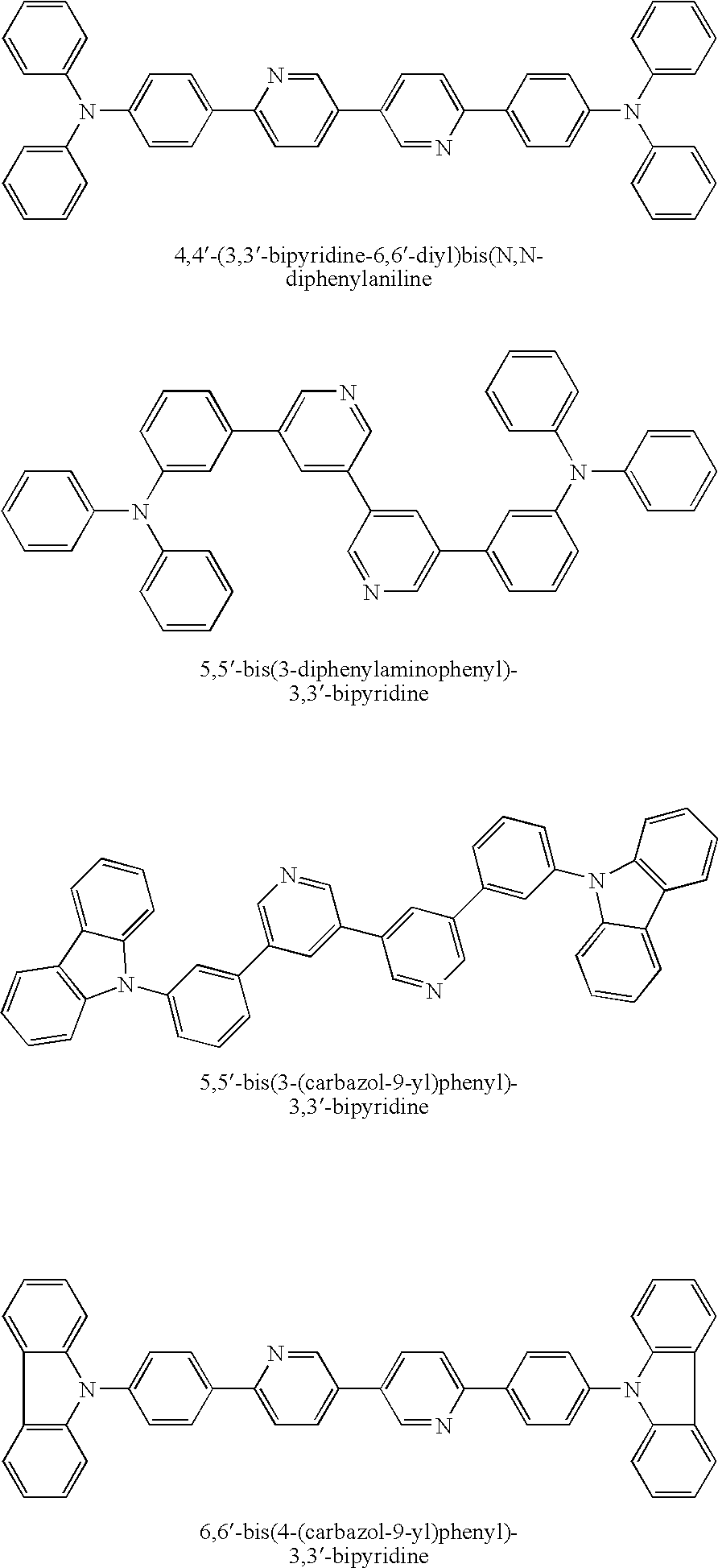
- Some embodiments also provide a compound selected from optionally substituted 5,5′-bis(diphenylamino)-3,3′-bipyridine, optionally substituted 6,6′-(dicarbazole-9-yl)-3,3′-bipyridine, optionally substituted 6,6′-bis(diphenylamino)-3,3′-bipyridine, optionally substituted 5,5′-(dicarbazole-9-yl)-3,3′-bipyridine, optionally substituted 5,5′-bis(4-diphenylaminophenyl)-3,3′-bipyridine, optionally substituted 5,5′-bis(4-(3,6-dimethylcarbazol-9-yl)phenyl)-3,3′-bipyridine, optionally substituted 5,5′-bis(4-(carbazol-9-yl)phenyl)-3,3′-bipyridine, optionally substituted 5,5′-bis(4-(carbazol-9-yl)phenyl)-3
- an organic light-emitting diode device comprising: a cathode; an anode; and an organic component, disposed between the anode and the cathode; wherein the organic component comprises a host compound described herein.
- FIG. 1 displays the spectroscopic properties of one embodiment of the host compound in CHCl 3 solution.
- FIG. 2 is a current density vs. voltage plot of two embodiments of the light-emitting devices.
- FIG. 3 is the electroluminescence spectrum of one embodiment of the light-emitting device.
- FIG. 4 is a current density vs. voltage curve of the light-emitting devices in FIG. 3 .
- FIG. 5 shows the EQE (external quantum efficiency) and the luminance efficiency with respect to the current density of the light-emitting device featured in FIG. 3 .
- alkyl refers to a fully saturated hydrocarbon moiety. Examples include, but are not limited to, linear alkyl, branched alkyl, cycloalkyl, or combinations thereof. Alkyl may be bonded to any other number of moieties (e.g. be bonded to 1 other group, such as —CH 3 , 2 other groups, such as —CH 2 —, or any number of other groups) that the structure may bear, and in some embodiments, may contain from one to thirty-five carbon atoms. Examples of alkyl groups include but are not limited to CH 3 (e.g. methyl), C 2 H 5 (e.g. ethyl), C 3 H 7 (e.g.
- propyl isomers such as propyl, isopropyl, etc.), C 3 H 6 (e.g. cyclopropyl), C 4 H 9 (e.g. butyl isomers) C 4 H 8 (e.g. cyclobutyl isomers such as cyclobutyl, methylcyclopropyl, etc.), C 5 H 11 (e.g. pentyl isomers), C 5 H 10 (e.g. cyclopentyl isomers such as cyclopentyl, methylcyclobutyl, dimethylcyclopropyl, etc.) C 6 H 13 (e.g. hexyl isomers), C 6 H 12 (e.g.
- cyclohexyl isomers C 7 H 15 (e.g. heptyl isomers), C 7 H 14 (e.g. cycloheptyl isomers), C 8 H 17 (e.g. octyl isomers), C 8 H 16 (e.g. cyclooctyl isomers), C 9 H 19 (e.g. nonyl isomers), C 9 H 18 (e.g. cyclononyl isomers), C 10 H 21 (e.g. decyl isomers), C 10 H 20 (e.g. cyclodecyl isomers), C 11 H 23 (e.g. undecyl isomers), C 11 H 22 (e.g.
- cycloundecyl isomers C 12 H 25 (e.g. dodecyl isomers), C 12 H 24 (e.g. cyclododecyl isomers), C 13 H 27 (e.g. tridecyl isomers), C 13 H 26 (e.g. cyclotridecyl isomers), and the like.
- Alkyl may also be defined by the following general formulas: the general formula for linear or branched fully saturated hydrocarbons not containing a cyclic structure is C n H 2n+2 , and the general formula for a fully saturated hydrocarbon containing one ring is C n H 2n .
- a C X-Y alkyl or C X -C Y alkyl is an alkyl having from X to Y carbon atoms.
- C 1-12 alkyl or C 1 -C 12 alkyl includes fully saturated hydrocarbon containing 1, 2, 3, 4, 5, 6, 7, 8, 9, 10, 11, or 12 carbon atoms.
- optionally substituted group refers to a group that may be substituted or unsubstituted.
- a substituted group is derived from the unsubstituted parent structure wherein one or more hydrogen atoms on the parent structure have been independently replaced by one or more substituent groups.
- a substituted group may have one or more substituent groups on the parent group structure.
- the substituent groups are independently selected from optionally substituted phenyl, optionally substituted alkyl, —O-alkyl (e.g. —OCH 3 , —OC 2 H 5 , —OC 3 H 2 , —OC 4 H 9 , etc.), —S-alkyl (e.g.
- Optionally substituted alkyl refers to unsubstituted alkyl and substituted alkyl.
- the substituted alkyl refers to substituted alkyl where one or more H atoms are replaced by one or more substituent groups, such as —O-alkyl (e.g. —OCH 3 , —OC 2 H 5 , —OC 3 H 7 , —OC 4 H 9 , etc.), —S-alkyl (e.g.
- R′ and R′′ are independently H or alkyl, —OH, —SH, —CN, —NO 2 , or a halogen.
- Some examples of optionally substituted alkyl may be alkyl, haloalkyl, perfluoroalkyl, hydroxyalkyl, alkylthiol (i.e. alkyl-SH), -alkyl-CN, etc.
- Optionally substituted C 1-12 alkyl refers to unsubstituted C 1-12 alkyl and substituted C 1-12 alkyl.
- the substituted C 1-12 alkyl refers to C 1-12 alkyl where one or more hydrogen atoms are independently replaced by one or more of the substituent groups indicated above.
- halogen refers to fluoro, chloro, bromo or iodo.
- fluoroalkyl refers to alkyl having one or more fluorine substituents. In other words, it is substituted alkyl where one or more hydrogen atoms are substituted by fluorine, but no other atoms except C, H, and F are present.
- C 1-6 F 1-13 fluoroalkyl refers to fluoroalkyl having 1-6 carbon atoms and 1-13 fluorine atoms.
- perfluoroalkyl refers to fluoroalkyl with a formula C 6 F 2n+1 for a linear or branched structure, e.g., CF 3 , C 2 F 5 , C 3 F 7 , C 4 F 9 , C 5 F 11 , C 6 F 13 , etc., or C n F 2n for a cyclic structure, e.g., cyclic C 3 F 6 , cyclic C 4 F 8 , cyclic C 5 F 10 , cyclic C 6 F 12 , etc.
- every hydrogen atom in alkyl is replaced by fluorine.
- C 1-3 perfluoroalkyl refers to CF 3 , C 2 F 5 , and C 3 F 7 isomers.
- optionally substituted phenyl refers to unsubstituted phenyl or substituted phenyl.
- substituted phenyl one or more hydrogen atoms on the ring system are independently replaced by one or more substituent groups indicated above.
- optionally substituted phenyl may be optionally substituted 1,4-interphenylene or optionally substituted 1,3-interphenylene.
- a “C2 symmetry axis” is an axis wherein rotating a molecule by 180° (i.e. 360°/2) about that axis yields the same structure. For example, in Formula 1, if: 1) R 1 is the same as R 8 , 2) R 2 is the same as R 7 , 3) R 3 is the same as R 6 , and 4) R 4 is the same as R 5 , then the molecule has a C2 symmetry axis.
- ambipolar material refers to a material that is capable of transferring both holes and electrons effectively.
- phosphorescent material refers to a material that can emit light from both singlet and triplet excitons.
- R 1 , R 2 , R 3 , R 6 , R 7 , and R 8 are independently selected from the group consisting of H, optionally substituted C 1-12 alkyl such as optionally substituted methyl, optionally substituted ethyl, optionally substituted propyl isomers, optionally substituted cyclopropyl, optionally substituted butyl isomers, optionally substituted cyclobutyl isomers (such as cyclobutyl, methylcyclopropyl, etc.), optionally substituted pentyl isomers, optionally substituted cyclopentyl isomers, optionally substituted hexyl isomers, optionally substituted cyclohexyl isomers, optionally substituted heptyl isomers, optionally substituted cycloheptyl isomers; optionally substituted octyl isomers, optionally substituted cyclooctyl isomers, optionally substituted nonyl is
- R 1 , R 2 , R 3 , R 6 , R 7 , and R 8 are independently selected from the group consisting of H, unsubstituted C 1-12 alkyl, C 1-12 alkyl having from 1 to 13 halogen substituents (such as CF 3 , C 2 F 5 , C 3 F 7 , C 4 F 9 , C 5 F 11 , C 6 F 13 , cyclic C 3 F 6 , cyclic C 4 F 8 , cyclic C 5 F 10 , cyclic C 6 F 12 , etc.), optionally substituted phenyl, optionally substituted carbazolyl, optionally substituted diphenylamine, optionally substituted carbazolylphenyl, and optionally substituted diphenylaminophenyl.
- halogen substituents such as CF 3 , C 2 F 5 , C 3 F 7 , C 4 F 9 , C 5 F 11 , C 6 F 13 , cyclic C 3 F 6 , cyclic C
- R 1 , R 3 , R 4 , R 5 , R 6 , and R 8 are H, and R 2 and R 7 are independently selected from optionally substituted carbazolyl, optionally substituted diphenylamine, optionally substituted carbazolylphenyl, and optionally substituted diphenylaminophenyl.
- At least one of R 1 , R 2 , and R 3 is selected from optionally substituted carbazolyl, optionally substituted diphenylamine, optionally substituted carbazolylphenyl, and optionally substituted diphenylaminophenyl and at least one of R 6 , R 7 , and R 8 is selected from optionally substituted carbazolyl, optionally substituted diphenylamine, optionally substituted carbazolylphenyl, and optionally substituted diphenylaminophenyl.
- R 4 and R 5 are independently selected from the group consisting of H, optionally substituted C 1-12 alkyl, optionally substituted phenyl, optionally substituted diphenylamine and optionally substituted diphenylaminophenyl.
- each pyridinyl ring of the bipyridine substructure has at least one optionally substituted carbazolyl, optionally substituted diphenylamine, optionally substituted carbazolylphenyl, or optionally substituted diphenylaminophenyl which is located in a position other than the ortho position between the ring nitrogen and the carbon that connects the two rings (i.e. the position of R 4 and R 5 ).
- R 2 and R 7 are independently selected from optionally substituted carbazolyl, optionally substituted diphenylamine, optionally substituted carbazolylphenyl, or optionally substituted diphenylaminophenyl.
- R 3 and R 6 are optionally substituted carbazolyl, optionally substituted diphenylamine, optionally substituted carbazolylphenyl, or optionally substituted diphenylaminophenyl.
- R 2 and R 7 are independently selected from optionally substituted carbazolyl, optionally substituted diphenylamine, optionally substituted carbazolylphenyl, or optionally substituted diphenylaminophenyl, and R 1 , R 3 , R 6 , and R 8 are independently H, C 1-8 alkyl, or C 1-3 perfluoroalkyl.
- R 3 and R 6 are optionally substituted carbazolyl, optionally substituted diphenylamine, optionally substituted carbazolylphenyl, or optionally substituted diphenylaminophenyl
- R 1 , R 2 , R 7 , and R 8 are independently H, C 1-8 alkyl, or C 1-3 perfluoroalkyl
- R 2 and R 7 are selected from optionally substituted carbazolyl, optionally substituted diphenylamine, optionally substituted carbazolylphenyl, and optionally substituted diphenylaminophenyl
- R 1 , R 3 , R 6 , and R 8 are H.
- R 3 and R 6 are optionally substituted carbazole, and R 1 , R 2 , R 7 , and R 8 are H.
- R 4 and R 5 are H.
- R 1 , R 3 , R 4 , R 5 , R 6 , and R 8 are H, and R 2 and R 7 are optionally substituted carbazolyl.
- the optionally substituted C 1-12 alkyl is unsubstituted C 1-12 alkyl, or C 1-12 alkyl substituted by 1 to 13 halogen atoms.
- the compound of Formula 1 has a C2 symmetry axis. In other embodiments, the compound of Formula 1 does not have a C2 symmetry axis.
- Some embodiments provide a compound represented by Formula 2:
- each dotted line is independently an optional bond.
- some embodiments relate to compounds represented by Formula 2A or Formula 2B.
- Ph 1 and Ph 2 are independently optionally substituted 1,4-interphenylene or optionally substituted 1,3-interphenylene.
- Ph 1 and Ph 2 may have 1, 2, or 3 substituents independently selected from C 1-6 alkyl and C 1-6 perfluoroalkyl.
- R 9 and R 10 are independently H, C 1-3 alkyl, or C 1-3 perfluoroalkyl; and R 11 , R 12 , R 13 , R 14 , R 15 , R 16 , R 17 , R 18 , R 19 , R 20 , R 21 , and R 22 are independently selected from the group consisting of H, C 1-12 alkyl, C 1-6 F 1-13 fluoroalkyl, and optionally substituted phenyl.
- R 9 and R 10 are H; R 9 and R 10 are CH 3 ; or, alternatively, R 9 and R 10 are CF 3 .
- R 11 is C 1-8 alkyl, or alternatively, phenyl.
- R 12 is C 1-8 alkyl, or alternatively, phenyl.
- R 11 , R 16 , R 17 , and R 22 are independently H or C 1-8 alkyl.
- R 11 , R 16 , R 17 , and R 22 are independently C 1-8 alkyl or phenyl.
- R 11 , R 16 , R 18 , and R 21 are independently H, C 1-8 alkyl or phenyl. In some embodiments, R 12 , R 15 , R 18 , and R 21 are independently H, C 1-8 alkyl or phenyl.
- inventions provide a compound selected from optionally substituted 5,5′-bis(diphenylamino)-3,3′-bipyridine, optionally substituted 6,6′-(dicarbazole-9-yl)-3,3′-bipyridine, optionally substituted 6,6′-bis(diphenylamino)-3,3′-bipyridine, optionally substituted 5,5′-(dicarbazole-9-yl)-3,3′-bipyridine, optionally substituted 5,5′-bis(4-diphenylaminophenyl)-3,3′-bipyridine, optionally substituted 5,5′-bis(4-(3,6-dimethylcarbazol-9-yl)phenyl)-3,3′-bipyridine, optionally substituted 5,5′-bis(4-(carbazol-9-yl)phenyl)-3,3′-bipyridine, optionally substituted 5,5′-bis(4-(carbazol-9-yl)phenyl)-3,3
- these compounds may be unsubstituted, or have 1, 2, 3, 4, 5, or 6 substituents independently selected from: C 1-12 alkyl; CF 3 ; and phenyl having 0, 1, or 2 substituents, wherein the substituents on phenyl are independently C 1-3 alkyl or CF 3 .
- Some embodiments provide a compound represented by Formula 3:
- R 9 and R 10 are independently H, CH 3 , or CF 3 ; and R 11 , R 12 , R 15 , R 16 , R 17 , R 18 , R 21 , and R 22 are independently H, unsubstituted phenyl, or C 1-8 alkyl.
- R 11 , R 16 , R 17 , and R 22 are independently H, C 1-8 alkyl, or phenyl.
- R 11 , R 16 , R 18 , and R 21 are independently H, C 1-8 alkyl or phenyl.
- R 12 , R 15 , R 18 , and R 21 are independently H, C 1-8 alkyl or phenyl.
- Some embodiments provide one of the compounds below.
- a light-emitting device may have a cathode, an anode, and an organic component comprising a compound described herein. At least one of the compounds described herein may be present in the organic component, and may be useful as a host material with electron-transfer properties, hole-transfer properties, or both electron-transfer and hole-transfer properties.
- the organic component comprises a light-emitting layer
- the device may be configured to allow holes to be transported from the anode to the light-emitting layer and allow electrons to be transported from the cathode to the light-emitting layer.
- the light-emitting layer may optionally comprise the host compound.
- the organic component may further comprise a hole-transport layer disposed between the anode and the light-emitting layer, and which may be configured to allow holes to be transported from the anode to the light-emitting layer.
- the organic component may further comprise an electron-transport layer disposed between the cathode and the light-emitting layer, which may be configured to allow electrons to be transported from the cathode to the light-emitting layer.
- At least one of the light-emitting layer, the hole-transport layer and the electron-transport layer comprise the host compound. In some embodiments, all of the light-emitting layer, the hole-transport layer and the electron-transport layer comprise the host compound. In one embodiment, the host is ambipolar, and its ability to transfer holes is about equal to its ability to transport electrons.
- An anode layer may comprise a conventional material such as a metal, mixed metal, alloy, metal oxide or mixed-metal oxide, or a conductive polymer.
- suitable metals include the Group 1 metals, the metals in Groups 4, 5, 6, and the Group 8-10 transition metals. If the anode layer is to be light-transmitting, mixed-metal oxides of Group 12, 13, and 14 metals or alloys thereof, such as Au, Pt, and indium-tin-oxide (ITO), may be used.
- the anode layer may include an organic material such as polyaniline, e.g., as described in “Flexible light-emitting diodes made from soluble conducting polymer,” Nature, vol. 357, pp. 477-479 (11 Jun.
- the anode layer can have a thickness in the range of about 1 nm to about 1000 nm.
- a cathode layer may include a material having a lower work function than the anode layer.
- suitable materials for the cathode layer include those selected from alkali metals of Group 1, Group 2 metals, Group 12 metals including rare earth elements, lanthanides and actinides, materials such as aluminum, indium, calcium, barium, samarium and magnesium, and combinations thereof.
- Li-containing organometallic compounds, LiF, and Li 2 O may also be deposited between the organic layer and the cathode layer to lower the operating voltage.
- Suitable low work function metals include but are not limited to Al, Ag, Mg, Ca, Cu, Mg/Ag, LiF/Al, CsF, CsF/Al or alloys thereof.
- the cathode layer can have a thickness in the range of about 1 nm to about 1000 nm.
- the light-emitting layer may further comprise a light-emitting component or compound.
- the light-emitting component may be a fluorescent and/or a phosphorescent compound.
- the light-emitting component comprises a phosphorescent material.
- the light-emitting component or compound may be chosen to vary the color of the light emitted by the light-emitting device.
- a blue light-emitting component may emit a combination of visible photons so that the light appears to have a blue quality to an observer.
- a blue light-emitting component may emit visible photons having an average wavelength in the range of about 440 nm or about 460 nm to about 490 nm or about 500 nm.
- iridium coordination compounds such as: bis- ⁇ 2-[3,5-bis(trifluoromethyl)phenyl]pyridinato-N,C2′ ⁇ iridium(III)-picolinate, bis(2-[4,6-difluorophenyl]pyridinato-N,C2′)iridium (III) picolinate, bis(2-[4,6-difluorophenyl]pyridinato-N,C2′)iridium(acetylacetonate), Iridium (III) bis(4,6-difluorophenylpyridinato)-3-(trifluoromethyl)-5-(pyridine-2-yl)-1,2,4-triazolate, Iridium (III) bis(4,6-difluorophenylpyridinato)-5-(pyridine-2-yl)-1H-tetrazolate, bis[2-(2-(3,5-bis(trifluoromethyl)phenyl]pyridinato-
- a red light-emitting component may emit a combination of visible photons so that the light appears to have a red quality to an observer.
- a red light-emitting component may emit visible photons having an average wavelength in the range of about 600 nm or about 620 nm to about 780 nm or about 800 nm.
- iridium coordination compounds such as: Bis[2-(2′-benzothienyl)-pyridinato-N,C3′]iridium (III)(acetylacetonate); Bis[(2-phenylquinolyl)-N,C2′]iridium (III) (acetylacetonate); Bis[(1-phenylisoquinolinato-N,C2′)]iridium (III) (acetylacetonate); Bis[(dibenzo[f,h]quinoxalino-N,C2′)iridium (III)(acetylacetonate); Tris(2,5-bis-2′-(9′,9′-dihexylfluorene)pyridine)iridium (III); Tris[1-phenylisoquinolinato-N,C2′]iridium (III); Tris-[2-(2′-benzothienyl)-pyridinato-N,C3′]iridium
- a green light-emitting component may emit a combination of visible photons so that the light appears to have a green quality to an observer.
- a green light-emitting component may emit visible photons having an average wavelength in the range of about 490 nm or about 500 nm to about 570 nm or about 600 nm.
- iridium coordination compounds such as: Bis(2-phenylpyridinato-N,C2′)iridium(III)(acetylacetonate) [Ir(ppy) 2 (acac)], Bis(2-(4-tolyl)pyridinato-N,C2′)iridium(III)(acetylacetonate) [Ir(mppy) 2 (acac)], Bis(2-(4-tert-butyl)pyridinato-N,C2′)iridium (III)(acetylacetonate) [Ir(t-Buppy) 2 (acac)], Tris(2-phenylpyridinato-N,C2′)iridium (III) [Ir(ppy) 3 ], Bis(2-phenyloxazolinato-N,C2′)iridium (III) (acetylacetonate) [Ir(Ir(ppy) 3 ], Bis(2-phenyloxazolinato-N,C2′
- An orange light-emitting component may emit a combination of visible photons so that the light appears to have a orange quality to an observer.
- an orange light-emitting component may emit visible photons having an average wavelength in the range of about 570 nm or about 585 nm to about 620 nm or about 650 nm.
- iridium coordination compounds such as: Bis[2-phenylbenzothiazolato-N,C2′]iridium (III)(acetylacetonate), Bis[2-(4-tert-butylphenyl)benzothiazolato-N,C2′]iridium(III)(acetylacetonate), Bis[(2-(2′-thienyl)pyridinato-N,C3′)]iridium (III) (acetylacetonate), Tris[2-(9.9-dimethylfluoren-2-yl)pyridinato-(N,C3′)]iridium (III), Tris[2-(9.9-dimethylfluoren-2-yl)pyridinato-(N,C3′)]iridium (III), Bis[5-trifluoromethyl-2-[3-(N-phenylcarbzoly
- a white light-emitting component may emit a combination of visible photons so that the light appears to have a white quality to an observer.
- a single compound may have multiple emissive moieties which independently emit different colored light.
- the emissive moieties may be covalently combined, such as in the examples below:
- Some single compounds comprising multiple emissive moieties may be metal coordination compounds, such as iridium or platinum coordination compounds, which have at least two different ligands. These ligands may have similar lifetimes so that at least two different colors of light may be simultaneously emitted from the same compound.
- metal coordination compounds such as iridium or platinum coordination compounds
- These ligands may have similar lifetimes so that at least two different colors of light may be simultaneously emitted from the same compound.
- the compound below is an example of such a compound
- Another type of single compound which may emit white light is a compound that can form excimers.
- the monomers and excimers may emit at different wavelengths, and may thus provide two different colors of emission which together may appear white light.
- Compounds may also emit white light by other methods, for example, a single compound may form an exciplex with adjacent layer compounds, which may result in white light emission for the device.
- a single compound may form an exciplex with adjacent layer compounds, which may result in white light emission for the device.
- a non-limiting example of such a compound is depicted below.
- White light may also be obtained by combining, either in a single layer or in multiple layers, at least two light-emitting components having different color emission. For example, a combination of a red light-emitting component, a blue light-emitting component, and a green light-emitting component, either in a single layer or in more than one layer, may provide white light. Alternatively a combination of a blue light-emitting component, and an orange light-emitting component, either in a single layer or in more than one layer, may provide white light.
- the amount of the light-emitting component may vary. In some embodiments, the light-emitting component may be about 0.1% (w/w) to about 5% (w/w), or about 1% (w/w) with respect to the host.
- the thickness of the light-emitting layer may vary. In some embodiments, the light-emitting layer has a thickness from about 1 nm to about 200 nm. In some embodiments, the light-emitting layer has a thickness in the range of about 1 nm to about 100 nm.
- the light-emitting layer can further include additional host material.
- host materials are known to those skilled in the art.
- the host material included in the light-emitting layer can be an optionally substituted compound selected from: an aromatic-substituted amine, an aromatic-substituted phosphine, a thiophene, an oxadiazole, 2-(4-biphenyl)-5-(4-tert-butylphenyl)-1,3,4-oxadiazole (PBD), 1,3-bis(N,N-t-butyl-phenyl)-1,3,4-oxadiazole (OXD-7), a triazole, 3-phenyl-4-(1′-naphthyl)-5-phenyl-1,2,4-triazole (TAZ), 3,4,5-Triphenyl-1,2,3-triazole, 3,5-Bis(4-tert-butyl-phenyl)-4-phenyl[1,
- the light-emitting device may further comprise a hole-transport layer between the anode and the light-emitting layer and an electron-transport layer between the cathode and the light-emitting layer. In some embodiments, all of the light-emitting layer, the hole-transport layer and the electron-transport layer comprise the host compound described herein.
- the hole-transport layer may comprise at least one hole-transport materials.
- Suitable hole-transport materials are known to those skilled in the art.
- Exemplary hole-transport materials include: 1,1-Bis(4-bis(4-methylphenyl)aminophenyl)cyclohexane; 2,9-Dimethyl-4,7-diphenyl-1,10-phenanthroline; 3,5-Bis(4-tert-butyl-phenyl)-4-phenyl[1,2,4]triazole; 3,4,5-Triphenyl-1,2,3-triazole; 4,4′,4′′-Tris(N-(naphthylen-2-yl)-N-phenylamino)triphenylamine; 4,4′,4′-tris(3-methylphenylphenylamino)triphenylamine (MTDATA); 4,4′-bis[N-(naphthyl)-N-phenyl-amino]biphenyl ( ⁇ -NPD
- the electron-transport layer may comprise at least one electron-transport materials.
- Suitable electron transport materials are known to those skilled in the art.
- Exemplary electron transport materials that can be included in the electron transport layer are an optionally substituted compound selected from: aluminum tris(8-hydroxyquinolate) (Alq3), 2-(4-biphenyl)-5-(4-tert-butylphenyl)-1,3,4-oxadiazole (PBD), 1,3-bis(N,N-t-butyl-phenyl)-1,3,4-oxadiazole (OXD-7), 1,3-bis[2-(2,2′-bipyridine-6-yl)-1,3,4-oxadiazo-5-yl]benzene (BPY-OXD), 3-phenyl-4-(1′-naphthyl)-5-phenyl-1,2,4-triazole (TAZ), 2,9-dimethyl-4,7-diphenyl-phenanthroline (bathocuproine or
- the electron transport layer is aluminum quinolate (Alq 3 ), 2-(4-biphenyl)-1)-5-(4-tert-butylphenyl)-1,3,4-oxadiazole (PBD), phenanthroline, quinoxaline, 1,3,5-tris[N-phenylbenzimidazol-z-yl]benzene (TPBI), or a derivative or a combination thereof.
- additional materials may be included in the light-emitting device. Additional materials that may be included include an electron injection materials, hole blocking materials, exciton blocking materials, and/or hole injection materials.
- the electron injection materials, hole blocking materials, exciton blocking materials, and/or hole injection materials may be incorporated into any of the layers described above, or may be incorporated into one or more separate layers, such as an electron injection layer, a hole blocking layer, an exciton blocking layer, and/or a hole injection layer.
- the light-emitting device can include an electron injection layer between the cathode layer and the light emitting layer.
- the lowest unoccupied molecular orbital (LUMO) energy level of the electron injection material(s) is high enough to prevent it from receiving an electron from the light emitting layer.
- the energy difference between the LUMO of the electron injection material(s) and the work function of the cathode layer is small enough to allow efficient electron injection from the cathode.
- suitable electron injection materials are known to those skilled in the art.
- suitable electron injection material(s) include but are not limited to, an optionally substituted compound selected from the following: aluminum quinolate (Alq 3 ), 2-(4-biphenyl)-1)-5-(4-tert-butylphenyl)-1,3,4-oxadiazole (PBD), phenanthroline, quinoxaline, 1,3,5-tris[N-phenylbenzimidazol-z-yl]benzene (TPBI) a triazine, a metal chelate of 8-hydroxyquinoline such as tris(8-hydroxyquinoliate) aluminum, and a metal thioxinoid compound such as bis(8-quinolinethiolato) zinc.
- Alq 3 aluminum quinolate
- PBD 2-(4-biphenyl)-1)-5-(4-tert-butylphenyl)-1,3,4-oxadiazole
- TPBI 1,3,5-tris[N-phenylbenzimidazol-z-yl]
- the electron injection layer is aluminum quinolate (Alq 3 ), 2-(4-biphenyl)-1)-5-(4-tert-butylphenyl)-1,3,4-oxadiazole (PBD), phenanthroline, quinoxaline, 1,3,5-tris[N-phenylbenzimidazol-z-yl]benzene (TPBI), or a derivative or a combination thereof.
- the device can include a hole blocking layer, e.g., between the cathode and the light-emitting layer.
- a hole blocking layer e.g., between the cathode and the light-emitting layer.
- suitable hole blocking materials that can be included in the hole blocking layer are known to those skilled in the art.
- Suitable hole blocking material(s) include but are not limited to, an optionally substituted compound selected from the following: bathocuproine (BCP), 3,4,5-triphenyl-1,2,4-triazole, 3,5-bis(4-tert-butyl-phenyl)-4-phenyl-[1,2,4]triazole, 2,9-dimethyl-4,7-diphenyl-1,10-phenanthroline, and 1,1-bis(4-bis(4-methylphenyl)aminophenyl)-cyclohexane.
- BCP bathocuproine
- 3,4,5-triphenyl-1,2,4-triazole 3,5-bis(4
- the light-emitting device can include an exciton blocking layer, e.g., between the light-emitting layer and the anode.
- the band gap of the exciton blocking material(s) is large enough to substantially prevent the diffusion of excitons.
- suitable exciton blocking materials that can be included in the exciton blocking layer are known to those skilled in the art.
- exciton blocking material(s) examples include an optionally substituted compound selected from the following: aluminum quinolate (Alq 3 ), 4,4′-bis[N-(naphthyl)-N-phenyl-amino]biphenyl ( ⁇ -NPD), 4,4′-N,N′-dicarbazole-biphenyl (CBP), and bathocuproine (BCP), and any other material(s) that have a large enough band gap to substantially prevent the diffusion of excitons.
- Alq 3 aluminum quinolate
- ⁇ -NPD 4,4′-bis[N-(naphthyl)-N-phenyl-amino]biphenyl
- CBP 4,4′-N,N′-dicarbazole-biphenyl
- BCP bathocuproine
- the light-emitting device can include a hole injection layer, e.g., between the light-emitting layer and the anode.
- a hole injection layer e.g., between the light-emitting layer and the anode.
- suitable hole injection materials that can be included in the hole injection layer are known to those skilled in the art.
- Exemplary hole injection material(s) include an optionally substituted compound selected from the following: a polythiophene derivative such as poly(3,4-ethylenedioxythiophene (PEDOT)/polystyrene sulphonic acid (PSS), a benzidine derivative such as N,N,N′,N′-tetraphenylbenzidine, poly(N,N′-bis(4-butylphenyl)-N,N′-bis(phenyl)benzidine), a triphenylamine or phenylenediamine derivative such as N,N′-bis(4-methylphenyl)-N,N′-bis(phenyl)-1,4-phenylenediamine, 4,4′,4′′-tris(N-(naphthylen-2-yl)-N-phenylamino)triphenylamine, an oxadiazole derivative such as 1,3-bis(5-(4-diphenylamino)phenyl-1,3,4
- the various materials described above can be incorporated in several different layers depending on the configuration of the device.
- the materials used in each layer are selected to result in the recombination of the holes and electrons in the light-emitting layer.
- Light-emitting devices comprising the compounds disclosed herein can be fabricated using techniques known in the art, as informed by the guidance provided herein.
- a glass substrate can be coated with a high work functioning metal such as ITO which can act as an anode.
- a light-emitting layer that includes at least a compound disclosed herein can be deposited on the anode.
- the cathode layer comprising a low work functioning metal (e.g., Mg:Ag), can then be vapor evaporated onto the light-emitting layer.
- the device can also include an electron transport/injection layer, a hole blocking layer, a hole injection layer, an exciton blocking layer and/or a second light-emitting layer that can be added to the device using techniques known in the art, as informed by the guidance provided herein.
- ITO coated glass substrates were cleaned by ultrasound in acetone and 2-propanol, consecutively, then baked at 110° C. for 3 hours, followed by treatment with oxygen plasma for 5 min.
- a layer of PEDOT: PSS (Baytron P from H. C. Starck) was spin-coated at 3000 rpm onto the pre-cleaned and O 2 -plasma treated (ITO)-substrate and annealed at 180° C. for 10 min, yielding a thickness of around 40 nm.
- TCTA 4,4′4′′-tri(N-carbazolyl)triphenylamine
- Dicbz-Bipy and platinum(II)(2-(4′,6′-difluorophenyl)pyridinato-N,C 2′ )(2,4-pentanedionato) (FPt) were concurrently heated and deposited on top of TCTA under different deposition speed to make FPt at 12 wt %, followed by deposition of 2,9-dimethyl-4,7-diphenyl-1,10-phenanthroline (BCP) at deposition rate around 0.06 nm/s.
- BCP 2,9-dimethyl-4,7-diphenyl-1,10-phenanthroline
- CsF and Al were then deposited successively at deposition rates of 0.005 and 0.2 nm/s, respectively.
- Each individual device has an area of 0.14 cm 2 .
- Device A was fabricated as following: ITO-coated glass substrates were cleaned by ultrasound in acetone and 2-propanol, consecutively, then baked at 110° C. for 3 hours, followed by treatment with oxygen plasma for 5 min.
- a layer of PEDOT: PSS (Baytron P from H. C. Starck) was spin-coated at 3000 rpm onto the pre-cleaned and O 2 -plasma treated (ITO)-substrate and annealed at 180° C. for 10 min, yielding a thickness of around 40 nm.
- Device B was fabricated as following: ITO-coated glass substrates were cleaned by ultrasound in acetone and 2-propanol, consecutively, then baked at 110° C. for 3 hours, followed by treatment with oxygen plasma for 5 min.
- the I-V spectra of Device A and Device B are shown in FIG. 2 , showing balanced hole-current and electron-current, indicating Dicbz-Bipy has ambipolar property. Note that there is no any detectable electroluminescence (EL) during the measurements in each device, ensuring uni-polar injection.
- EL electrolum
- Electroluminescence (EL) spectrum of Device C was collected at two different driving voltages, 5.5 V and 8 A ( FIG. 3 ).
- the CIE and CRI values were also determined at different driving voltages.
- the CIE color coordinates (X, Y) is defined as the achromatic point.
- the X and Y color coordinates are weights applied to the CIE primaries to match a color.
- the color rendering index refers to the ability to render various colors and has values ranging from 0 to 100, with 100 being the best.
- CIE color rendering index
- the CIE of Device C was (0.45, 0.46) and the CRI value was 73.
- the CIE was (0.43, 0.46), and the CRI value was 70.
- FIG. 4 shows the turn-on voltage for Device C and the maximum luminance was about 8000 cd/m 2 .
- FIG. 5 shows the EQE (external quantum efficiency) and luminous efficiency as a function of current density.
- the EQE of Device C was about 11.8%, and the luminous efficiency was about 26.4 cd/A.
- the power efficiency (PE) was 14.5 lm/w at 1000 cd/m 2 .
- the usefulness of the compound disclosed herein is demonstrated by their charge mobility.
- the carrier mobility of an organic thin film can be derived from the space charge limited current in the current-voltage (IV) measurement based on the Mott's steady state SCLC model
- ⁇ 0 is the vacuum permittivity
- ⁇ is the relative permittivity of the organic layer
- ⁇ is the carrier mobility of the organic layer
- V is the voltage bias
- L is the thickness of the organic layer.
- Electron-only devices may have Al/organic layer/LiF/Al structure with Al as the anode and LiF/Al as the cathode.
- the LiF/Al electrode has a low work function ( ⁇ 2.6 eV) which can facilitate the injection of electrons into the lower lying LUMO of the organic layer.
- Al has a relatively lower work function (4.28 eV) than the HOMO (5 ⁇ 6 eV) of the organic layer being investigated, which prevents the hole injection from the anode.
- the electron mobility may be measured as the only charge carrier in the organic layer.
- the hole-only devices may have the ITO/PEDOT/organic layer/Al with ITO as the anode and Al as the cathode.
- the high work function of PEDOT (5.2-5.4 eV) facilitates hole injection from the anode into the organic layer.
- the work function (4.28 eV) of Al is higher than the LUMO of the organic layer (2 ⁇ 4 eV), which preventing the electron injection from the cathode.
- the hole mobility may be measured as the only charge carrier in the organic layer.
- the thickness of the organic layer is kept at 100 nm in both cases.
- Electron- and hole-mobility can be derived from the electron-only and hole-only devices for the same organic layer, respectively.
- the substrates ITO coated glass for hole-only devices and glass for electron only devices
- the substrates were cleaned by detergent, ultrasonic bath in acetone and consecutively in 2-propanol, and baked at 110° C. for 3 hours.
- the precleaned ITO substrates first underwent a UV-ozone treatment for 30 min.
- a layer of PEDOT: PSS (Baytron P purchased from H. C. Starck) was spin-coated at 6000 rpm onto the substrates and annealed at 180° C. in a glove box for 30 min, yielding a thickness of around 20 nm.
- a 100 nm-thick layer of the organic compound to be evaluated was first deposited by thermal evaporation on top of PEDOT/PSS layer at deposition rate of 0.1 nm/s.
- a 50 nm-thick Al layer was then deposited successively by thermal evaporation at deposition rate of 0.3 nm/s, through a shadow mask to define the device area.
- the device areas for hole-only and electron-only devices are 0.08 and 0.04 cm 2 , respectively.
- I-V measurements were carried out using a Keithley 2400 Source Meter to apply 0-10 V voltage scans and measure the current simultaneously. All device operations were done inside a nitrogen-filled glove-box. The high-current end of the IV curves (6-10 V) were fitted by the SCLC model
- the electron- and hole-mobility can then be derived from the fitting parameters for the electron-only and hole-only devices, respectively.
- This method may be adapted to any host compound by replacing the JC-HT3 with the host compound to be tested.
Abstract

wherein R1, R2, R3, R6, R7, and R8 are independently selected from the group consisting of H, optionally substituted C1-12 alkyl, optionally substituted phenyl, optionally substituted carbazolyl, optionally substituted diphenylamine and optionally substituted diphenylaminophenyl; provided that: at least one of R1, R2, and R3 is selected from optionally substituted carbazolyl, optionally substituted diphenylamine and optionally substituted diphenylaminophenyl and at least one of R6, R7, and R8 is selected from optionally substituted carbazolyl, optionally substituted diphenylamine and optionally substituted diphenylaminophenyl; and R4 and R5 are independently selected from the group consisting of H, optionally substituted C1-12 alkyl, optionally substituted phenyl, optionally substituted diphenylamine and optionally substituted diphenylaminophenyl. Other embodiments provide an organic light-emitting diode device comprising a compound of Formula I.
Description

wherein R1, R2, R3, R6, R7, and R8 are independently selected from the group consisting of H, optionally substituted C1-12 alkyl, optionally substituted phenyl, optionally substituted carbazolyl, optionally substituted diphenylamine, optionally substituted carbazolylphenyl, and optionally substituted diphenylaminophenyl; provided that: at least one of R1, R2, and R3 is selected from optionally substituted carbazolyl, optionally substituted diphenylamine, optionally substituted carbazolylphenyl, and optionally substituted diphenylaminophenyl and at least one of R6, R7, and R8 is selected from optionally substituted carbazolyl, optionally substituted diphenylamine, optionally substituted carbazolylphenyl, and optionally substituted diphenylaminophenyl; and R4 and R5 are independently selected from the group consisting of H, optionally substituted C1-12 alkyl, optionally substituted phenyl, optionally substituted diphenylamine and optionally substituted diphenylaminophenyl.

wherein each dotted line is independently an optional bond, Ph1 and Ph2 are independently optionally substituted 1,4-interphenylene or optionally substituted 1,3-interphenylene, y and z are independently 0 or 1; R9 and R10 are independently H, C1-3 alkyl, or C1-3 perfluoroalkyl; and R11, R12, R13, R14, R15, R16, R17, R18, R19, R20, R21, and R22 are independently selected from the group consisting of H, C1-12 alkyl, C1-6F1-13 fluoroalkyl, and optionally substituted phenyl.


wherein R9 and R10 are independently H, CH3, or CF3; and R11, R12, R15, R16, R17, R18, R21, and R22 are independently H, unsubstituted phenyl, or C1-8 alkyl. In some embodiments, R11, R16, R17, and R22 are independently H, C1-8 alkyl, or phenyl. In other embodiments, R11, R16, R18, and R21 are independently H, C1-8 alkyl or phenyl. In other embodiments, R12, R15, R18, and R21 are independently H, C1-8 alkyl or phenyl.


The electron- and hole-mobility can then be derived from the fitting parameters for the electron-only and hole-only devices, respectively. This method may be adapted to any host compound by replacing the JC-HT3 with the host compound to be tested.
Claims (20)


Priority Applications (1)
| Application Number | Priority Date | Filing Date | Title |
|---|---|---|---|
| US12/694,939 US8062771B2 (en) | 2009-02-03 | 2010-01-27 | Ambipolar host in organic light emitting diode |
Applications Claiming Priority (2)
| Application Number | Priority Date | Filing Date | Title |
|---|---|---|---|
| US14956009P | 2009-02-03 | 2009-02-03 | |
| US12/694,939 US8062771B2 (en) | 2009-02-03 | 2010-01-27 | Ambipolar host in organic light emitting diode |
Publications (2)
| Publication Number | Publication Date |
|---|---|
| US20100213452A1 US20100213452A1 (en) | 2010-08-26 |
| US8062771B2 true US8062771B2 (en) | 2011-11-22 |
Family
ID=41800649
Family Applications (7)
| Application Number | Title | Priority Date | Filing Date |
|---|---|---|---|
| US12/694,920 Active US8062770B2 (en) | 2009-02-03 | 2010-01-27 | Ambipolar host in organic light emitting diode |
| US12/694,939 Active 2030-01-31 US8062771B2 (en) | 2009-02-03 | 2010-01-27 | Ambipolar host in organic light emitting diode |
| US12/694,984 Active US8003229B2 (en) | 2009-02-03 | 2010-01-27 | Ambipolar host in organic light emitting diode |
| US12/694,981 Expired - Fee Related US8062772B2 (en) | 2009-02-03 | 2010-01-27 | Ambipolar host in organic light emitting diode |
| US12/694,994 Active US8062773B2 (en) | 2009-02-03 | 2010-01-27 | Ambipolar host in organic light emitting diode |
| US12/695,000 Active US8057921B2 (en) | 2009-02-03 | 2010-01-27 | Ambipolar host in organic light emitting diode |
| US13/280,703 Active US8263238B2 (en) | 2009-02-03 | 2011-10-25 | Ambipolar host in organic light emitting diode |
Family Applications Before (1)
| Application Number | Title | Priority Date | Filing Date |
|---|---|---|---|
| US12/694,920 Active US8062770B2 (en) | 2009-02-03 | 2010-01-27 | Ambipolar host in organic light emitting diode |
Family Applications After (5)
| Application Number | Title | Priority Date | Filing Date |
|---|---|---|---|
| US12/694,984 Active US8003229B2 (en) | 2009-02-03 | 2010-01-27 | Ambipolar host in organic light emitting diode |
| US12/694,981 Expired - Fee Related US8062772B2 (en) | 2009-02-03 | 2010-01-27 | Ambipolar host in organic light emitting diode |
| US12/694,994 Active US8062773B2 (en) | 2009-02-03 | 2010-01-27 | Ambipolar host in organic light emitting diode |
| US12/695,000 Active US8057921B2 (en) | 2009-02-03 | 2010-01-27 | Ambipolar host in organic light emitting diode |
| US13/280,703 Active US8263238B2 (en) | 2009-02-03 | 2011-10-25 | Ambipolar host in organic light emitting diode |
Country Status (7)
| Country | Link |
|---|---|
| US (7) | US8062770B2 (en) |
| EP (1) | EP2393900B1 (en) |
| JP (1) | JP5367095B2 (en) |
| KR (1) | KR101853014B1 (en) |
| CN (1) | CN102341476B (en) |
| TW (1) | TWI429636B (en) |
| WO (1) | WO2010090925A1 (en) |
Cited By (4)
| Publication number | Priority date | Publication date | Assignee | Title |
|---|---|---|---|---|
| US20120037900A1 (en) * | 2009-02-03 | 2012-02-16 | Nitto Denko Corporation | Ambipolar host in organic light emitting diode |
| US9328086B2 (en) | 2010-09-16 | 2016-05-03 | Nitto Denko Corporation | Substituted bipyridines for use in organic light-emitting devices |
| US9328094B2 (en) | 2011-09-19 | 2016-05-03 | Nitto Denko Corporation | Substituted biaryl compounds for light-emitting devices |
| US10573829B2 (en) | 2011-02-16 | 2020-02-25 | Semiconductor Energy Laboratory Co., Ltd. | Light-emitting element |
Families Citing this family (37)
| Publication number | Priority date | Publication date | Assignee | Title |
|---|---|---|---|---|
| KR101763424B1 (en) | 2009-04-21 | 2017-08-02 | 동우 화인켐 주식회사 | White-emitting compounds using excited-state intramolecular proton transfer, organinc electroluminescent element and laser material using the same |
| US20110260141A1 (en) * | 2009-10-29 | 2011-10-27 | E.I. Du Pont De Nemours And Company | Organic light-emitting diode luminaires |
| WO2011149500A1 (en) * | 2010-01-07 | 2011-12-01 | Nitto Denko Corporation | Emissive compounds for organic light-emitting diodes |
| EP3115434B1 (en) * | 2010-01-20 | 2019-07-17 | Hitachi, Ltd. | Organic luminescent materials, coating solution using same for organic emitting layer, organic light emitting device using coating solution and light source device using organic light emitting device |
| JP4945645B2 (en) * | 2010-01-20 | 2012-06-06 | 株式会社日立製作所 | Organic light emitting layer material, organic light emitting layer forming coating liquid using organic light emitting layer material, organic light emitting element using organic light emitting layer forming coating liquid, and light source device using organic light emitting element |
| TWI429650B (en) * | 2010-02-12 | 2014-03-11 | Nippon Steel & Sumikin Chem Co | Organic electroluminescent elements |
| JP5649327B2 (en) * | 2010-04-22 | 2015-01-07 | ユー・ディー・シー アイルランド リミテッド | Organic electroluminescence device |
| WO2011156414A2 (en) * | 2010-06-11 | 2011-12-15 | Nitto Denko Corporation | Light-emitting devices for phototherapy |
| CN101974036B (en) * | 2010-10-21 | 2012-10-03 | 华东师范大学 | Fluorene and spiro-fluorene substituted phenylpyridine iridium complex and preparation method and application thereof |
| EP2638578A1 (en) * | 2010-11-11 | 2013-09-18 | Nitto Denko Corporation | Hybrid composite emissive construct and light-emitting devices using the same |
| JP5771965B2 (en) * | 2010-12-09 | 2015-09-02 | コニカミノルタ株式会社 | Multicolor phosphorescent organic electroluminescence device and lighting device |
| JPWO2012115219A1 (en) * | 2011-02-25 | 2014-07-07 | 保土谷化学工業株式会社 | Compound having bipyridyl group and carbazole ring, and organic electroluminescence device |
| TWI526418B (en) * | 2011-03-01 | 2016-03-21 | 諾瓦發光二極體股份公司 | Organic semiconductive materials and organic component |
| EP2684933A4 (en) * | 2011-03-10 | 2014-09-03 | Univ Kyushu | Phosphorescent material, process for producing phosphorescent material, and phosphorescent element |
| WO2013039914A1 (en) | 2011-09-12 | 2013-03-21 | Nitto Denko Corporation | Efficient organic light-emitting diodes and fabrication of the same |
| US20130103123A1 (en) * | 2011-10-14 | 2013-04-25 | Sazzadur Rahman Khan | Light-Emitting Devices for Wound Healing |
| TWI670098B (en) * | 2011-10-14 | 2019-09-01 | 日商日東電工股份有限公司 | Light-emitting devices for wound healing,phototherapy system,and use of the device or the system |
| JP5205527B2 (en) * | 2012-03-02 | 2013-06-05 | 株式会社日立製作所 | Organic light emitting layer material, organic light emitting layer forming coating liquid using organic light emitting layer material, organic light emitting element using organic light emitting layer forming coating liquid, and light source device using organic light emitting element |
| KR102082111B1 (en) * | 2012-05-24 | 2020-02-27 | 메르크 파텐트 게엠베하 | Metal complexes comprising condensed heteroaromatic rings |
| US9859517B2 (en) | 2012-09-07 | 2018-01-02 | Nitto Denko Corporation | White organic light-emitting diode |
| JP5645984B2 (en) * | 2013-02-18 | 2014-12-24 | 株式会社日立製作所 | Organic light emitting layer material, organic light emitting layer forming coating liquid using organic light emitting layer material, organic light emitting element using organic light emitting layer forming coating liquid, and light source device using organic light emitting element |
| CN104017566A (en) * | 2013-02-28 | 2014-09-03 | 海洋王照明科技股份有限公司 | Bipolar blue-phosphorescence material, preparation method thereof and organic electroluminescent device |
| KR101598661B1 (en) | 2013-04-24 | 2016-02-29 | 주식회사 엘지화학 | Novel compound, preparation method thereof and organic light-emitting diode using the same |
| CN106488965A (en) | 2013-05-09 | 2017-03-08 | 日东电工株式会社 | Luminophor for luminescent device |
| KR102086555B1 (en) * | 2013-08-14 | 2020-03-10 | 삼성디스플레이 주식회사 | Anthracene-based compounds and Organic light emitting device comprising the same |
| CN107302844A (en) | 2013-10-30 | 2017-10-27 | 日东电工株式会社 | Luminophor for luminescent device |
| KR102289329B1 (en) * | 2013-12-02 | 2021-08-12 | 가부시키가이샤 한도오따이 에네루기 켄큐쇼 | Light-emitting element, light-emitting device, electronic appliance, and lighting device |
| WO2015195837A1 (en) | 2014-06-17 | 2015-12-23 | Nitto Denko Corporation | Emissive material for organic emitting diodes |
| WO2016041802A1 (en) * | 2014-09-16 | 2016-03-24 | Cynora Gmbh | Light-emitting layer suitable for bright luminescence |
| US9957280B2 (en) | 2014-12-15 | 2018-05-01 | Samsung Electronics Co., Ltd. | Luminescent compound and electroluminescent device exhibiting thermally activated delayed fluorescence |
| WO2016116517A1 (en) * | 2015-01-20 | 2016-07-28 | Cynora Gmbh | Pyridines and derivatives thereof as components for use in optoelectronic components |
| US10170521B2 (en) | 2015-12-30 | 2019-01-01 | Lg Display Co., Ltd. | Organic light-emitting diode display device |
| US10988447B2 (en) | 2016-06-30 | 2021-04-27 | Samsung Electronics Co., Ltd. | Bipyridine derivatives and their uses for organic light emitting diodes |
| TWI660028B (en) * | 2018-07-13 | 2019-05-21 | 祥德科技股份有限公司 | Light emitting layer host material for organic light emitting element |
| CN110343091A (en) * | 2019-06-17 | 2019-10-18 | 武汉华星光电半导体显示技术有限公司 | Optocoupler exports material and preparation method thereof, electroluminescent device |
| TW202122381A (en) * | 2019-09-30 | 2021-06-16 | 日商日鐵化學材料股份有限公司 | Organic electroluminescent element |
| TW202114987A (en) * | 2019-09-30 | 2021-04-16 | 日商日鐵化學材料股份有限公司 | Organic electroluminescent element |
Citations (20)
| Publication number | Priority date | Publication date | Assignee | Title |
|---|---|---|---|---|
| US20020024293A1 (en) | 2000-07-17 | 2002-02-28 | Fuji Photo Film Co., Ltd. | Light-emitting element and iridium complex |
| US20020034656A1 (en) | 1998-09-14 | 2002-03-21 | Thompson Mark E. | Organometallic complexes as phosphorescent emitters in organic LEDs |
| US20030072964A1 (en) * | 2001-10-17 | 2003-04-17 | Kwong Raymond C. | Phosphorescent compounds and devices comprising the same |
| US20030124381A1 (en) * | 2001-12-28 | 2003-07-03 | Thompson Mark E. | White light emitting OLEDs from combined monomer and aggregate emission |
| WO2003078541A1 (en) | 2002-03-15 | 2003-09-25 | Idemitsu Kosan Co., Ltd. | Material for organic electroluminescent devices and organic electroluminescent devices made by using the same |
| US20040024293A1 (en) | 2001-11-21 | 2004-02-05 | Matthew Lawrence | Methods and systems for analyzing complex biological systems |
| WO2004074399A1 (en) | 2003-02-20 | 2004-09-02 | Idemitsu Kosan Co., Ltd. | Material for organic electroluminescent device and organic electroluminescent device using same |
| JP2004273190A (en) | 2003-03-06 | 2004-09-30 | Konica Minolta Holdings Inc | Organic electroluminescent element, organic electroluminescent element material, display device, and lighting unit |
| US20050282036A1 (en) * | 2001-05-16 | 2005-12-22 | D Andrade Brian | High efficiency multi-color electro-phosphorescent OLEDs |
| WO2006080229A1 (en) | 2005-01-25 | 2006-08-03 | Pioneer Corporation | Organic compound, charge transport material and organic electroluminescent device |
| US20060222886A1 (en) | 2005-04-04 | 2006-10-05 | Raymond Kwong | Arylpyrene compounds |
| US20070015006A1 (en) | 2005-07-15 | 2007-01-18 | Lee Jun Y | White organic light emitting diode |
| US20070075631A1 (en) | 2005-10-04 | 2007-04-05 | Yeh Tung | Electron impeding layer for high efficiency phosphorescent OLEDs |
| JP2007291092A (en) | 2006-03-30 | 2007-11-08 | Chisso Corp | New bipyridine derivative and organic electroluminescence element containing the same |
| EP1857521A1 (en) | 2005-02-21 | 2007-11-21 | Mitsubishi Chemical Corporation | Organic electric field light emitting element and production therefor |
| WO2008027132A1 (en) | 2006-08-31 | 2008-03-06 | Universal Display Corporation | Charge transforting layer for organic electroluminescent device |
| JP2008115131A (en) * | 2006-11-07 | 2008-05-22 | Mitsubishi Chemicals Corp | Organic compound, charge-transporting material, composition for charge-transporting material, and organic electroluminescent element |
| JP2008120696A (en) | 2006-11-08 | 2008-05-29 | Chemiprokasei Kaisha Ltd | Novel tripyridylphenyl derivative, electron-transporting material comprising the same and organoelectroluminescent element comprising the same |
| US20080166591A1 (en) | 2006-12-27 | 2008-07-10 | Canon Kabushiki Kaisha | Carbazole compound and organic light-emitting device using same |
| WO2010090925A1 (en) | 2009-02-03 | 2010-08-12 | Nitto Denko Corporation | Ambipolar host in organic light emitting diode |
Family Cites Families (8)
| Publication number | Priority date | Publication date | Assignee | Title |
|---|---|---|---|---|
| GB9825524D0 (en) * | 1998-11-20 | 1999-01-13 | Oxford Biomedica Ltd | Vector |
| JP4006862B2 (en) * | 1998-12-22 | 2007-11-14 | コニカミノルタホールディングス株式会社 | Novel amino compound, its production method and use |
| AU2003281040A1 (en) | 2002-07-10 | 2004-02-02 | Sumitomo Pharmaceuticals Co., Ltd. | Biaryl derivatives |
| JP2008133225A (en) * | 2006-11-29 | 2008-06-12 | Toyo Ink Mfg Co Ltd | Indole derivative and application thereof |
| JP2008156266A (en) * | 2006-12-22 | 2008-07-10 | Chisso Corp | Electron transporting material and organic electroluminescent device produced by using the same |
| JP5176343B2 (en) * | 2007-03-07 | 2013-04-03 | Jnc株式会社 | Electron transport material and organic electroluminescent device using the same |
| JP2008214306A (en) * | 2007-03-07 | 2008-09-18 | Chisso Corp | Electron transport material and organic electroluminescent element using the same |
| WO2011156414A2 (en) | 2010-06-11 | 2011-12-15 | Nitto Denko Corporation | Light-emitting devices for phototherapy |
-
2010
- 2010-01-27 US US12/694,920 patent/US8062770B2/en active Active
- 2010-01-27 JP JP2011548257A patent/JP5367095B2/en active Active
- 2010-01-27 WO PCT/US2010/022260 patent/WO2010090925A1/en active Application Filing
- 2010-01-27 US US12/694,939 patent/US8062771B2/en active Active
- 2010-01-27 EP EP10702199.0A patent/EP2393900B1/en active Active
- 2010-01-27 KR KR1020117020281A patent/KR101853014B1/en active IP Right Grant
- 2010-01-27 US US12/694,984 patent/US8003229B2/en active Active
- 2010-01-27 US US12/694,981 patent/US8062772B2/en not_active Expired - Fee Related
- 2010-01-27 CN CN201080010223.6A patent/CN102341476B/en active Active
- 2010-01-27 US US12/694,994 patent/US8062773B2/en active Active
- 2010-01-27 US US12/695,000 patent/US8057921B2/en active Active
- 2010-02-02 TW TW099103024A patent/TWI429636B/en active
-
2011
- 2011-10-25 US US13/280,703 patent/US8263238B2/en active Active
Patent Citations (22)
| Publication number | Priority date | Publication date | Assignee | Title |
|---|---|---|---|---|
| US20020034656A1 (en) | 1998-09-14 | 2002-03-21 | Thompson Mark E. | Organometallic complexes as phosphorescent emitters in organic LEDs |
| US20020024293A1 (en) | 2000-07-17 | 2002-02-28 | Fuji Photo Film Co., Ltd. | Light-emitting element and iridium complex |
| US20050282036A1 (en) * | 2001-05-16 | 2005-12-22 | D Andrade Brian | High efficiency multi-color electro-phosphorescent OLEDs |
| US20030072964A1 (en) * | 2001-10-17 | 2003-04-17 | Kwong Raymond C. | Phosphorescent compounds and devices comprising the same |
| US20040024293A1 (en) | 2001-11-21 | 2004-02-05 | Matthew Lawrence | Methods and systems for analyzing complex biological systems |
| US20030124381A1 (en) * | 2001-12-28 | 2003-07-03 | Thompson Mark E. | White light emitting OLEDs from combined monomer and aggregate emission |
| WO2003078541A1 (en) | 2002-03-15 | 2003-09-25 | Idemitsu Kosan Co., Ltd. | Material for organic electroluminescent devices and organic electroluminescent devices made by using the same |
| US20050127823A1 (en) | 2002-03-15 | 2005-06-16 | Idemitsu Kosan Co., Ltd. | Material for organic electroluminescent devices and organic electroluminescent devices made by using the same |
| WO2004074399A1 (en) | 2003-02-20 | 2004-09-02 | Idemitsu Kosan Co., Ltd. | Material for organic electroluminescent device and organic electroluminescent device using same |
| JP2004273190A (en) | 2003-03-06 | 2004-09-30 | Konica Minolta Holdings Inc | Organic electroluminescent element, organic electroluminescent element material, display device, and lighting unit |
| WO2006080229A1 (en) | 2005-01-25 | 2006-08-03 | Pioneer Corporation | Organic compound, charge transport material and organic electroluminescent device |
| EP1858094A1 (en) | 2005-01-25 | 2007-11-21 | Pioneer Corporation | Organic compound, charge transport material and organic electroluminescent device |
| EP1857521A1 (en) | 2005-02-21 | 2007-11-21 | Mitsubishi Chemical Corporation | Organic electric field light emitting element and production therefor |
| US20060222886A1 (en) | 2005-04-04 | 2006-10-05 | Raymond Kwong | Arylpyrene compounds |
| US20070015006A1 (en) | 2005-07-15 | 2007-01-18 | Lee Jun Y | White organic light emitting diode |
| US20070075631A1 (en) | 2005-10-04 | 2007-04-05 | Yeh Tung | Electron impeding layer for high efficiency phosphorescent OLEDs |
| JP2007291092A (en) | 2006-03-30 | 2007-11-08 | Chisso Corp | New bipyridine derivative and organic electroluminescence element containing the same |
| WO2008027132A1 (en) | 2006-08-31 | 2008-03-06 | Universal Display Corporation | Charge transforting layer for organic electroluminescent device |
| JP2008115131A (en) * | 2006-11-07 | 2008-05-22 | Mitsubishi Chemicals Corp | Organic compound, charge-transporting material, composition for charge-transporting material, and organic electroluminescent element |
| JP2008120696A (en) | 2006-11-08 | 2008-05-29 | Chemiprokasei Kaisha Ltd | Novel tripyridylphenyl derivative, electron-transporting material comprising the same and organoelectroluminescent element comprising the same |
| US20080166591A1 (en) | 2006-12-27 | 2008-07-10 | Canon Kabushiki Kaisha | Carbazole compound and organic light-emitting device using same |
| WO2010090925A1 (en) | 2009-02-03 | 2010-08-12 | Nitto Denko Corporation | Ambipolar host in organic light emitting diode |
Non-Patent Citations (21)
| Title |
|---|
| Adachi, et al., Nearly 100% Internal Phosphorescence Efficiency in an Organic Light Emitting Device, J. Appl. Phys. 90, 5048, 2001. |
| Baldo, et al., High-Efficiency Fluorescent Organic Light-Emitting Devices Using a Phosphorescent Sensitizer, Nature, 403, 750, 2000. |
| Cai, et al., Electron and Hole Transport in a Wide Bandgap Organic Phosphine Oxide for Blue Electrophosphorescence, Appl. Phys. Lett. 92, 083308, 2008. |
| Chen, et al., White Organic Light-Emitting Devices with a Bipolar Transport Layer Between Blue Fluorescent and Orange Phosphorescent Emitting Layers, Appl. Phys. Lett. 91, 023505, 2007. |
| Cheng, et al., White Organic Light-Emitting Devices Using a Phosphorescent Sensitizer, Appl. Phys. Lett. 82, 4224, 2003. |
| D'Andrade, et al., Efficient Organic Electrophosphorescent White-Light-Emitting Device with a Triple Doped Emissive Layer, Adv. Mater. 16, 624, 2004. |
| D'Andrade, et al., White Light Emission Using Triplet Excimers in Electrophosphorescent Organic Light-Emitting Devices, Adv. Mater. 14, 1032, 2002. |
| D'Andrade, et al., White Organic Light-Emitting Devices for Solid-State Lighting, Adv. Mater. 16, 1585, 2004. |
| Guan, et al., The Host Materials Containing Carbazole and Oxadiazole Fragment for Red Triplet Emitter in Organic Light-Emitting Diodes, Org. Electronics, 7, 330-336, 2006. |
| Kido, et al., Pyridine-Containing Bipolar Host Materials for Hightly Efficient Blue Phosphorescent OLED's, Chem. Mater. 2008, 20(5), 1691-1693. |
| Machine translation for JP2004-273190, Sep. 2004 in 44 pages. |
| Machine-generated translation for JP 2004-273190, which was published Sep. 2004. * |
| Office Action in U.S. Appl. No. 12/694,920, dated Feb. 18, 2011. |
| Office Action in U.S. Appl. No. 12/694,981, dated Mar. 18, 2011. |
| Office Action in U.S. Appl. No. 12/694,984, dated Mar. 17, 2011. |
| Office Action in U.S. Appl. No. 12/694,994, dated Mar. 17, 2011. |
| Office Action in U.S. Appl. No. 12/695,000, dated Mar. 25, 2011. |
| Seo, et al., Highly Efficient White Organic Light-Emitting Diodes using Two Emitting Materials for Three Primary Colors (red, green, and blue), Appl. Phys. Lett. 90, 203507, 2007. |
| Su Shi-Jian, et al., "Pyridine-Containing Bipolar Host Materials for Highly Efficient Blue Phosphorescent OLEDs" Chemistry of Materials, American Chemical Society, Washington, US, vol. 20, Jan. 1, 2008, pp. 1691-1693, XP002535894, ISSN: 0897-4756. |
| Sun, et al., Management of Singlet and Triplet Excitons for Efficient White Organic Light-Emitting Devices, Nature,440, 908, 2006. |
| Wu, et al., Highly Efficient White-Electrophosphorescent Devices Based on Polyfluorene Copolymers Containing Charge-Transporting Pendent Units, J. Mater. Chem. 17, 167, 2007. |
Cited By (7)
| Publication number | Priority date | Publication date | Assignee | Title |
|---|---|---|---|---|
| US20120037900A1 (en) * | 2009-02-03 | 2012-02-16 | Nitto Denko Corporation | Ambipolar host in organic light emitting diode |
| US8263238B2 (en) * | 2009-02-03 | 2012-09-11 | Nitto Denko Corporation | Ambipolar host in organic light emitting diode |
| US9328086B2 (en) | 2010-09-16 | 2016-05-03 | Nitto Denko Corporation | Substituted bipyridines for use in organic light-emitting devices |
| US10573829B2 (en) | 2011-02-16 | 2020-02-25 | Semiconductor Energy Laboratory Co., Ltd. | Light-emitting element |
| US10586934B2 (en) | 2011-02-16 | 2020-03-10 | Semiconductor Energy Laboratory Co., Ltd. | Light-emitting element |
| US10593895B2 (en) | 2011-02-16 | 2020-03-17 | Semiconductor Energy Laboratory Co., Ltd. | Light-emitting element |
| US9328094B2 (en) | 2011-09-19 | 2016-05-03 | Nitto Denko Corporation | Substituted biaryl compounds for light-emitting devices |
Also Published As
| Publication number | Publication date |
|---|---|
| US8263238B2 (en) | 2012-09-11 |
| US20100213829A1 (en) | 2010-08-26 |
| JP2012516848A (en) | 2012-07-26 |
| US8003229B2 (en) | 2011-08-23 |
| EP2393900A1 (en) | 2011-12-14 |
| US8062770B2 (en) | 2011-11-22 |
| TW201036956A (en) | 2010-10-16 |
| US20100213831A1 (en) | 2010-08-26 |
| US20100213830A1 (en) | 2010-08-26 |
| US8057921B2 (en) | 2011-11-15 |
| EP2393900B1 (en) | 2013-04-17 |
| US20120037900A1 (en) | 2012-02-16 |
| US20100213832A1 (en) | 2010-08-26 |
| CN102341476A (en) | 2012-02-01 |
| JP5367095B2 (en) | 2013-12-11 |
| US8062772B2 (en) | 2011-11-22 |
| US20100213452A1 (en) | 2010-08-26 |
| US8062773B2 (en) | 2011-11-22 |
| KR20110126648A (en) | 2011-11-23 |
| US20100213453A1 (en) | 2010-08-26 |
| CN102341476B (en) | 2014-10-29 |
| KR101853014B1 (en) | 2018-06-07 |
| TWI429636B (en) | 2014-03-11 |
| WO2010090925A1 (en) | 2010-08-12 |
Similar Documents
| Publication | Publication Date | Title |
|---|---|---|
| US8062771B2 (en) | Ambipolar host in organic light emitting diode | |
| US8974922B2 (en) | Phenylcarbazole-based compounds and fluorene-based compounds and organic light emitting device and flat panel display device comprising the same | |
| US9028979B2 (en) | Phenanthroazole compounds as hole transporting materials for electro luminescent devices | |
| US8604689B2 (en) | Hybrid composite emissive construct and light-emitting devices using the same | |
| WO2011048822A1 (en) | Organic electroluminescent element | |
| US20100326526A1 (en) | Emissive aryl-heteroaryl compounds | |
| WO2011048821A1 (en) | Organic electroluminescent element | |
| US9328094B2 (en) | Substituted biaryl compounds for light-emitting devices | |
| US20120214269A1 (en) | Tetraphenylsilane compounds suitable as organic hole-transport materials | |
| US8585926B2 (en) | Substituted bipyridines for use in light-emitting devices | |
| US9425408B2 (en) | Organic light emitting host materials | |
| US8785002B1 (en) | High-energy triplet host materials, luminescent layer comprising the same, and organic electroluminescent device comprising the luminescent layer | |
| US8895157B2 (en) | Host material for lighting devices | |
| US20140284584A1 (en) | Organic light emitting bipolar host materials | |
| US20100231125A1 (en) | Organic light emitting device to emit in near infrared | |
| US20230006161A1 (en) | Organic light-emitting device | |
| US11482679B2 (en) | Compound, light-emitting lifetime lengthening agent, use of n-type compound, film and light-emitting device | |
| US9172051B2 (en) | Organic light emitting host materials | |
| US9343684B2 (en) | Substituted bisaryloxybiphenyl compounds for use in light-emitting devices | |
| US20140367663A1 (en) | Emissive iridium complexes for light-emitting devices |
Legal Events
| Date | Code | Title | Description |
|---|---|---|---|
| AS | Assignment |
Owner name: NITTO DENKO CORPORATION, JAPAN Free format text: ASSIGNMENT OF ASSIGNORS INTEREST;ASSIGNORS:SISK, DAVID T.;LI, SHENG;MOCHIZUKI, AMANE;REEL/FRAME:024353/0819 Effective date: 20100504 |
|
| STCF | Information on status: patent grant |
Free format text: PATENTED CASE |
|
| FPAY | Fee payment |
Year of fee payment: 4 |
|
| AS | Assignment |
Owner name: SAMSUNG ELECTRONICS CO., LTD., KOREA, REPUBLIC OF Free format text: ASSIGNMENT OF ASSIGNORS INTEREST;ASSIGNOR:NITTO DENKO CORPORATION;REEL/FRAME:042756/0388 Effective date: 20170404 |
|
| MAFP | Maintenance fee payment |
Free format text: PAYMENT OF MAINTENANCE FEE, 8TH YEAR, LARGE ENTITY (ORIGINAL EVENT CODE: M1552); ENTITY STATUS OF PATENT OWNER: LARGE ENTITY Year of fee payment: 8 |
|
| MAFP | Maintenance fee payment |
Free format text: PAYMENT OF MAINTENANCE FEE, 12TH YEAR, LARGE ENTITY (ORIGINAL EVENT CODE: M1553); ENTITY STATUS OF PATENT OWNER: LARGE ENTITY Year of fee payment: 12 |