US8071474B2 - Method of manufacturing semiconductor device suitable for forming wiring using damascene method - Google Patents
Method of manufacturing semiconductor device suitable for forming wiring using damascene method Download PDFInfo
- Publication number
- US8071474B2 US8071474B2 US12/853,676 US85367610A US8071474B2 US 8071474 B2 US8071474 B2 US 8071474B2 US 85367610 A US85367610 A US 85367610A US 8071474 B2 US8071474 B2 US 8071474B2
- Authority
- US
- United States
- Prior art keywords
- film
- wiring
- semiconductor device
- cvd
- manufacture method
- Prior art date
- Legal status (The legal status is an assumption and is not a legal conclusion. Google has not performed a legal analysis and makes no representation as to the accuracy of the status listed.)
- Active
Links
Images


Classifications
-
- H—ELECTRICITY
- H01—ELECTRIC ELEMENTS
- H01L—SEMICONDUCTOR DEVICES NOT COVERED BY CLASS H10
- H01L21/00—Processes or apparatus adapted for the manufacture or treatment of semiconductor or solid state devices or of parts thereof
- H01L21/70—Manufacture or treatment of devices consisting of a plurality of solid state components formed in or on a common substrate or of parts thereof; Manufacture of integrated circuit devices or of parts thereof
- H01L21/71—Manufacture of specific parts of devices defined in group H01L21/70
- H01L21/768—Applying interconnections to be used for carrying current between separate components within a device comprising conductors and dielectrics
- H01L21/76838—Applying interconnections to be used for carrying current between separate components within a device comprising conductors and dielectrics characterised by the formation and the after-treatment of the conductors
- H01L21/76841—Barrier, adhesion or liner layers
- H01L21/76843—Barrier, adhesion or liner layers formed in openings in a dielectric
-
- H—ELECTRICITY
- H01—ELECTRIC ELEMENTS
- H01L—SEMICONDUCTOR DEVICES NOT COVERED BY CLASS H10
- H01L21/00—Processes or apparatus adapted for the manufacture or treatment of semiconductor or solid state devices or of parts thereof
- H01L21/02—Manufacture or treatment of semiconductor devices or of parts thereof
- H01L21/04—Manufacture or treatment of semiconductor devices or of parts thereof the devices having at least one potential-jump barrier or surface barrier, e.g. PN junction, depletion layer or carrier concentration layer
- H01L21/18—Manufacture or treatment of semiconductor devices or of parts thereof the devices having at least one potential-jump barrier or surface barrier, e.g. PN junction, depletion layer or carrier concentration layer the devices having semiconductor bodies comprising elements of Group IV of the Periodic System or AIIIBV compounds with or without impurities, e.g. doping materials
- H01L21/28—Manufacture of electrodes on semiconductor bodies using processes or apparatus not provided for in groups H01L21/20 - H01L21/268
- H01L21/283—Deposition of conductive or insulating materials for electrodes conducting electric current
- H01L21/285—Deposition of conductive or insulating materials for electrodes conducting electric current from a gas or vapour, e.g. condensation
- H01L21/28506—Deposition of conductive or insulating materials for electrodes conducting electric current from a gas or vapour, e.g. condensation of conductive layers
- H01L21/28512—Deposition of conductive or insulating materials for electrodes conducting electric current from a gas or vapour, e.g. condensation of conductive layers on semiconductor bodies comprising elements of Group IV of the Periodic System
- H01L21/28556—Deposition of conductive or insulating materials for electrodes conducting electric current from a gas or vapour, e.g. condensation of conductive layers on semiconductor bodies comprising elements of Group IV of the Periodic System by chemical means, e.g. CVD, LPCVD, PECVD, laser CVD
-
- H—ELECTRICITY
- H01—ELECTRIC ELEMENTS
- H01L—SEMICONDUCTOR DEVICES NOT COVERED BY CLASS H10
- H01L21/00—Processes or apparatus adapted for the manufacture or treatment of semiconductor or solid state devices or of parts thereof
- H01L21/70—Manufacture or treatment of devices consisting of a plurality of solid state components formed in or on a common substrate or of parts thereof; Manufacture of integrated circuit devices or of parts thereof
- H01L21/71—Manufacture of specific parts of devices defined in group H01L21/70
- H01L21/768—Applying interconnections to be used for carrying current between separate components within a device comprising conductors and dielectrics
- H01L21/76801—Applying interconnections to be used for carrying current between separate components within a device comprising conductors and dielectrics characterised by the formation and the after-treatment of the dielectrics, e.g. smoothing
- H01L21/76829—Applying interconnections to be used for carrying current between separate components within a device comprising conductors and dielectrics characterised by the formation and the after-treatment of the dielectrics, e.g. smoothing characterised by the formation of thin functional dielectric layers, e.g. dielectric etch-stop, barrier, capping or liner layers
- H01L21/76831—Applying interconnections to be used for carrying current between separate components within a device comprising conductors and dielectrics characterised by the formation and the after-treatment of the dielectrics, e.g. smoothing characterised by the formation of thin functional dielectric layers, e.g. dielectric etch-stop, barrier, capping or liner layers in via holes or trenches, e.g. non-conductive sidewall liners
-
- H—ELECTRICITY
- H01—ELECTRIC ELEMENTS
- H01L—SEMICONDUCTOR DEVICES NOT COVERED BY CLASS H10
- H01L21/00—Processes or apparatus adapted for the manufacture or treatment of semiconductor or solid state devices or of parts thereof
- H01L21/70—Manufacture or treatment of devices consisting of a plurality of solid state components formed in or on a common substrate or of parts thereof; Manufacture of integrated circuit devices or of parts thereof
- H01L21/71—Manufacture of specific parts of devices defined in group H01L21/70
- H01L21/768—Applying interconnections to be used for carrying current between separate components within a device comprising conductors and dielectrics
- H01L21/76838—Applying interconnections to be used for carrying current between separate components within a device comprising conductors and dielectrics characterised by the formation and the after-treatment of the conductors
- H01L21/76841—Barrier, adhesion or liner layers
- H01L21/76843—Barrier, adhesion or liner layers formed in openings in a dielectric
- H01L21/76844—Bottomless liners
-
- H—ELECTRICITY
- H01—ELECTRIC ELEMENTS
- H01L—SEMICONDUCTOR DEVICES NOT COVERED BY CLASS H10
- H01L21/00—Processes or apparatus adapted for the manufacture or treatment of semiconductor or solid state devices or of parts thereof
- H01L21/70—Manufacture or treatment of devices consisting of a plurality of solid state components formed in or on a common substrate or of parts thereof; Manufacture of integrated circuit devices or of parts thereof
- H01L21/71—Manufacture of specific parts of devices defined in group H01L21/70
- H01L21/768—Applying interconnections to be used for carrying current between separate components within a device comprising conductors and dielectrics
- H01L21/76838—Applying interconnections to be used for carrying current between separate components within a device comprising conductors and dielectrics characterised by the formation and the after-treatment of the conductors
- H01L21/76841—Barrier, adhesion or liner layers
- H01L21/76853—Barrier, adhesion or liner layers characterized by particular after-treatment steps
- H01L21/76855—After-treatment introducing at least one additional element into the layer
-
- H—ELECTRICITY
- H01—ELECTRIC ELEMENTS
- H01L—SEMICONDUCTOR DEVICES NOT COVERED BY CLASS H10
- H01L21/00—Processes or apparatus adapted for the manufacture or treatment of semiconductor or solid state devices or of parts thereof
- H01L21/70—Manufacture or treatment of devices consisting of a plurality of solid state components formed in or on a common substrate or of parts thereof; Manufacture of integrated circuit devices or of parts thereof
- H01L21/71—Manufacture of specific parts of devices defined in group H01L21/70
- H01L21/768—Applying interconnections to be used for carrying current between separate components within a device comprising conductors and dielectrics
- H01L21/76838—Applying interconnections to be used for carrying current between separate components within a device comprising conductors and dielectrics characterised by the formation and the after-treatment of the conductors
- H01L21/76841—Barrier, adhesion or liner layers
- H01L21/76853—Barrier, adhesion or liner layers characterized by particular after-treatment steps
- H01L21/76861—Post-treatment or after-treatment not introducing additional chemical elements into the layer
- H01L21/76864—Thermal treatment
-
- H—ELECTRICITY
- H01—ELECTRIC ELEMENTS
- H01L—SEMICONDUCTOR DEVICES NOT COVERED BY CLASS H10
- H01L21/00—Processes or apparatus adapted for the manufacture or treatment of semiconductor or solid state devices or of parts thereof
- H01L21/70—Manufacture or treatment of devices consisting of a plurality of solid state components formed in or on a common substrate or of parts thereof; Manufacture of integrated circuit devices or of parts thereof
- H01L21/71—Manufacture of specific parts of devices defined in group H01L21/70
- H01L21/768—Applying interconnections to be used for carrying current between separate components within a device comprising conductors and dielectrics
- H01L21/76838—Applying interconnections to be used for carrying current between separate components within a device comprising conductors and dielectrics characterised by the formation and the after-treatment of the conductors
- H01L21/76841—Barrier, adhesion or liner layers
- H01L21/76867—Barrier, adhesion or liner layers characterized by methods of formation other than PVD, CVD or deposition from a liquids
-
- H—ELECTRICITY
- H01—ELECTRIC ELEMENTS
- H01L—SEMICONDUCTOR DEVICES NOT COVERED BY CLASS H10
- H01L21/00—Processes or apparatus adapted for the manufacture or treatment of semiconductor or solid state devices or of parts thereof
- H01L21/70—Manufacture or treatment of devices consisting of a plurality of solid state components formed in or on a common substrate or of parts thereof; Manufacture of integrated circuit devices or of parts thereof
- H01L21/71—Manufacture of specific parts of devices defined in group H01L21/70
- H01L21/768—Applying interconnections to be used for carrying current between separate components within a device comprising conductors and dielectrics
- H01L21/76838—Applying interconnections to be used for carrying current between separate components within a device comprising conductors and dielectrics characterised by the formation and the after-treatment of the conductors
- H01L21/76841—Barrier, adhesion or liner layers
- H01L21/76871—Layers specifically deposited to enhance or enable the nucleation of further layers, i.e. seed layers
- H01L21/76873—Layers specifically deposited to enhance or enable the nucleation of further layers, i.e. seed layers for electroplating
-
- H—ELECTRICITY
- H01—ELECTRIC ELEMENTS
- H01L—SEMICONDUCTOR DEVICES NOT COVERED BY CLASS H10
- H01L23/00—Details of semiconductor or other solid state devices
- H01L23/52—Arrangements for conducting electric current within the device in operation from one component to another, i.e. interconnections, e.g. wires, lead frames
- H01L23/522—Arrangements for conducting electric current within the device in operation from one component to another, i.e. interconnections, e.g. wires, lead frames including external interconnections consisting of a multilayer structure of conductive and insulating layers inseparably formed on the semiconductor body
- H01L23/532—Arrangements for conducting electric current within the device in operation from one component to another, i.e. interconnections, e.g. wires, lead frames including external interconnections consisting of a multilayer structure of conductive and insulating layers inseparably formed on the semiconductor body characterised by the materials
- H01L23/53204—Conductive materials
- H01L23/53209—Conductive materials based on metals, e.g. alloys, metal silicides
- H01L23/53228—Conductive materials based on metals, e.g. alloys, metal silicides the principal metal being copper
- H01L23/53233—Copper alloys
-
- H—ELECTRICITY
- H01—ELECTRIC ELEMENTS
- H01L—SEMICONDUCTOR DEVICES NOT COVERED BY CLASS H10
- H01L23/00—Details of semiconductor or other solid state devices
- H01L23/52—Arrangements for conducting electric current within the device in operation from one component to another, i.e. interconnections, e.g. wires, lead frames
- H01L23/522—Arrangements for conducting electric current within the device in operation from one component to another, i.e. interconnections, e.g. wires, lead frames including external interconnections consisting of a multilayer structure of conductive and insulating layers inseparably formed on the semiconductor body
- H01L23/532—Arrangements for conducting electric current within the device in operation from one component to another, i.e. interconnections, e.g. wires, lead frames including external interconnections consisting of a multilayer structure of conductive and insulating layers inseparably formed on the semiconductor body characterised by the materials
- H01L23/53204—Conductive materials
- H01L23/53209—Conductive materials based on metals, e.g. alloys, metal silicides
- H01L23/53228—Conductive materials based on metals, e.g. alloys, metal silicides the principal metal being copper
- H01L23/53238—Additional layers associated with copper layers, e.g. adhesion, barrier, cladding layers
-
- H—ELECTRICITY
- H01—ELECTRIC ELEMENTS
- H01L—SEMICONDUCTOR DEVICES NOT COVERED BY CLASS H10
- H01L2924/00—Indexing scheme for arrangements or methods for connecting or disconnecting semiconductor or solid-state bodies as covered by H01L24/00
- H01L2924/0001—Technical content checked by a classifier
- H01L2924/0002—Not covered by any one of groups H01L24/00, H01L24/00 and H01L2224/00
Definitions
- the present invention relates to a semiconductor device manufacture method, and more particularly to a semiconductor device manufacture method suitable for forming wirings by a damascene method by which a concave portion formed in an interlayer insulating film is filled with a conductive member.
- a delay of a signal transmitting along a wiring is becoming a dominant factor of lowering an operation speed of the logical element.
- the delay of a signal transmitting along a wiring is proportional to a product of a wiring resistance and a parasitic capacitance between wirings.
- a copper wiring is formed by the damascene method
- the inner surface of a wiring trench and a via hole is covered with a barrier layer before the copper film is deposited, the main object of the barrier layer being to prevent diffusion of copper into an insulating film.
- Refractory metal such as tantalum (Ta) and tungsten (W) is used as the material of a barrier film. Refractory metal has a resistivity higher than that of copper.
- the barrier layer has a large factor of raising a wiring resistance.
- a fine multi-layer wiring structure having a diameter and wiring width of a via hole of 0.1 ⁇ m or smaller, it is desired to make the barrier layer as thin as possible.
- a seed layer of CuMn alloy is formed by sputtering on the surface of an interlayer insulating film formed with wiring trenches and via holes. Thereafter, copper is electroplated to fill the wiring groove and via hole with the copper. Heat treatment is performed to react Si and O as the constituent elements in the interlayer insulating film with Mn as the constituent element in the seed layer.
- a barrier layer is therefore formed at the interface between a Cu wiring and the interlayer insulating film, the barrier layer being made of MnSi x O y compound which is very thin about 2 to 3 nm in thickness and has a uniform thickness. This barrier layer prevents diffusion of Cu.
- the seed layer covering the bottom of the via hole does not contact the interlayer insulating film and contacts a lower level wiring. Therefore, the barrier layer is not formed at the interface between the copper wiring in the via hole and the lower level wiring, so that the upper and lower level wirings can be connected without the barrier layer between the upper and lower level wirings. Further, since the barrier layer made of MnSiO compound can be made thinner than a barrier layer made of refractory metal, it is possible to suppress an increase of wiring resistance.
- the barrier layer has also a function of enhancing tight adhesion of the copper wiring.
- the barrier layer made of MnSiO compound is not formed during the period after the seed layer of CuMn alloy is formed and before heat treatment is executed.
- the present inventors have found that sufficient tight adhesion is not obtained between the seed layer and interlayer insulating film in such a state where the barrier layer is not formed. More specifically, a copper wiring may be peeled off after copper is electroplated and before heat treatment is executed.
- Tight adhesion was evaluated by forming 25 samples which have CuMn alloy layers having a thickness of 90 nm formed on a surface of each of silicon oxide films, porous methylsilsesquioxane (porous MSQ) films, SiCN films and SiOC films. Tape tests were conducted and peel-off arose in all samples. Tape tests were conducted after heat treatment for one minute at 300° C. in a nitrogen atmosphere, and peel-off did not arise in any samples. This may be ascribed to improved tight adhesion because heat treatment forms a barrier layer of MnSiO compound. It can be understood from this that the state before heat treatment does not ensure sufficient tight adhesion.
- a semiconductor device manufacture method comprising steps of: (a1) forming a concave portion in an interlayer insulating film formed on a semiconductor substrate; (a2) forming a first film of Mn by CVD, the first film covering an inner surface of the concave portion and an upper surface of the insulating film; (a3) depositing conductive material essentially consisting of Cu on the first film to embed the conductive material in the concave portion; and (a4) annealing the semiconductor substrate.
- a semiconductor device manufacture method comprising steps of: (b1) forming a concave portion in an interlayer insulating film formed on a semiconductor substrate; (b2) forming a first film containing Cu and Mn by CVD, the first film covering an inner surface of the concave portion and an upper surface of the insulating film; (b3) depositing conductive material essentially consisting of Cu on the first film to embed the conductive material in the concave portion; and (b4) annealing the semiconductor substrate.
- a semiconductor device manufacture method comprising steps of: (c1) forming a concave portion in an interlayer insulating film formed on a semiconductor substrate; (c2) forming a first film containing Cu and Mn by sputtering, the first film covering an inner surface of the concave portion and an upper surface of the insulating film; (c3) forming a second film of conductive material essentially consisting of Cu by CVD on the first film; and (c4) embedding conductive material essentially consisting of Cu in the concave portion.
- Sufficient adhesion can be ensured by forming the first film by CVD in the step (a2) or (b2). If the first film is formed by sputtering in the step (c2), tight adhesion can be ensured while the second film is formed by CVD in the step (c2).
- FIG. 1 is a cross sectional view of a semiconductor device manufactured by a semiconductor device manufacture method according to an embodiment.
- FIG. 2 is a table showing materials of an underlying film and a conductive member and film forming methods adopted by semiconductor device manufacture methods according to the first to ninth embodiments.
- FIGS. 3A to 3F are cross sectional views of a device during manufacture, illustrating the semiconductor device manufacture method according to the first embodiment.
- FIG. 4 is a schematic diagram showing a CVD system to be used by the semiconductor device manufacture methods of the embodiments.
- FIGS. 5A to 5C are cross sectional views of a device during manufacture, illustrating the semiconductor device manufacture method according to the fifth embodiment.
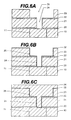
- FIGS. 6A to 6C are cross sectional views of a device during manufacture, illustrating the semiconductor device manufacture method according to the seventh embodiment.
- FIGS. 7A and 7B are cross sectional views of a device during manufacture, illustrating the semiconductor device manufacture method according to the ninth embodiment.
- FIG. 1 is a schematic cross sectional view of a semiconductor device manufactured by an embodiment method.
- An element isolation insulating film 2 is formed in a surface layer of a semiconductor substrate 1 by shallow trench isolation (STI) to define a plurality of active regions.
- a MOS transistor 3 is formed in an active region.
- the MOS transistor 3 is constituted of a source region 3 S, a drain region 3 D, a gate insulating film 31 and a gate electrode 3 G.
- An interlayer insulating film 4 of silicon oxide having a thickness of 300 nm and a protective film 6 of SiOC having a thickness of 50 nm are formed on the semiconductor substrate 1 , covering the MOS transistor 3 .
- a via hole is formed through the protective film 6 and interlayer insulating film 4 , to expose a partial surface of the drain region 3 D on the bottom of the via hole.
- a conductive plug 5 B of tungsten (W) is embedded in the via hole.
- a barrier metal layer 5 A of TiN having a thickness of 25 nm is disposed between the conductive plug 5 B and the inner surface of the via hole.
- the structure described above can be formed by well-known photolithography, etching, chemical vapor deposition (CVD), chemical mechanical polishing (CMP) and the like.
- An interlayer insulating film 10 made of low dielectric constant insulating material is formed on the protective film 6 .
- a wiring trench is formed in the interlayer insulating film 10 , reaching the bottom of the film 10 and crossing over the conductive plug 5 B.
- a first layer copper wiring 11 is embedded in the wiring trench. The copper wiring 11 is connected to the conductive plug 5 B.
- a cap film 20 , a via interlayer insulating film 21 , an etching stopper film 22 and a wiring interlayer insulating film 23 are formed on the interlayer insulating film 10 in this order recited.
- a wiring trench 25 is formed in the wiring interlayer insulating film 23 , and a via hole 24 is formed in the via interlayer insulating film 21 .
- the wiring trench 25 reaches the upper surface of the etching stopper film 22 .
- the via hole 24 opens on the bottom of the wiring trench 25 and reaches the upper surface of the lower level wiring 11 through the cap film 20 .
- a conductive member 30 of copper or copper alloy is embedded in the wiring trench 25 and via hole 24 .
- the conductive member 30 is connected to the first layer wiring 11 to constitute a second layer wiring.
- the detailed structure including the barrier layer will be later described in each of the embodiments.
- a cap film 50 , a via interlayer insulating film 51 , an etching stopper film 52 and a wiring interlayer insulating film 53 are stacked on the wiring interlayer insulating film 23 . Similar to the second level wiring structure, a wiring trench 55 and a via hole 54 are formed and a conductive member 60 is deposited therein. The conductive member 60 constitutes a third layer wiring.
- FIG. 2 shows a list of materials and deposition methods of an underlying film and a conductive member when a wiring or conductive member is formed by the methods of the first to ninth embodiments.
- CVD chemical vapor deposition
- SPUTTER vapor deposition method
- EP electroplating method
- the second layer wiring structure is formed by a dual damascene method.
- the third layer wiring structure is formed by the same method as that used for the second layer wiring structure.
- the first layer wiring 11 is formed by a single damascene method, and a barrier layer forming method, a method of depositing a conductive member in the wiring trench are the same as those adopted in the method of forming the second layer wiring structure.
- a cap film 20 , a via interlayer insulating film 21 , an etching stopper film 22 and a wiring interlayer insulating film 23 are sequentially formed on an interlayer insulating film 10 .
- the cap film 20 has a two-layer structure of a silicon oxide (SiO) film and a silicon carbide (SiC) film, and has a total thickness of 20 to 70 nm.
- the etching stopper film 22 is made of SiC or silicon nitride (SiN) and has a thickness of 20 to 70 nm. These films can be formed by CVD.
- the interlayer insulating films 21 and 23 are made of organic or inorganic low dielectric constant insulating material and have a thickness of 300 to 700 nm.
- the inorganic low dielectric constant insulating material may be porous silica or SiOC.
- the organic low dielectric constant insulating material may be SiLK (registered trademark) manufactured by the Dow Chemical Company. These materials contain Si and O as the constituent elements.
- a wiring trench 25 is formed through the wiring interlayer insulating film 23 , and a via hole 24 is formed through the via interlayer insulating film 21 .
- the size of the via hole 24 in a plan cross section is 0.06 to 0.1 ⁇ m and a minimum width of the wiring trench 25 is 0.06 ⁇ m.
- the wiring trench 25 and via hole 24 can be formed by dry etching using CF-containing etching gas and by using a hard mask constituted of, for example, two layers of an SiO film and an SiC film.
- the wiring trench 25 reaches the upper surface of the etching stopper film 22 , and the via hole 24 reaches the upper surface of the first layer wiring 11 .
- Mn is deposited by CVD on the upper surface of the wiring interlayer insulating film 23 , the inner surface of the wiring trench 25 and the inner surface of the via hole 24 to thereby form a first film 32 having a thickness of about 2 nm.
- Cu is deposited by CVD to form a second film 33 .
- a preferred thickness of the second film 33 is determined by the size of a plan pattern of the via hole 24 .
- the “size of a plan pattern” means a diameter of a circle inscribed to the plan pattern of the via hole 24 .
- the size of the plan pattern is the diameter of the circle, whereas if the plan cross section is a square, the size of the plan pattern is the length of one side of the square.
- the size of the plan pattern of the via hole is called “via diameter”. If the via diameter is 70 nm, a preferred thickness of the second film 23 is about 10 nm.
- FIG. 4 is a schematic diagram of a CVD system.
- a substrate stage 101 is disposed in a chamber 100 .
- a vacuum pump 103 evacuates and exhausts the air in the chamber 100 .
- a heater 102 is mounted in the substrate stage 101 .
- a semiconductor substrate 120 to be processed is held on the upper surface of the substrate stage 101 .
- a shower head 104 is disposed above the substrate stage 101 .
- Carrier gas e.g., H 2 gas and liquid source material of Cu is supplied to a carburetor 105 .
- Trimethylvinylsilyl-hexafluoroacetylacetonate copper (I) (hereinafter expressed as “Cu (hfac) tmvs) is used as Cu source material.
- Cu liquid source material is vaporized in the carburetor 105 and supplied to a gas flow path 110 together with the carrier gas.
- Carrier gas e.g., H 2 gas and Mn source material is supplied to a mass flow controller (MFC) 106 .
- MFC mass flow controller
- Bismethylcyclopentadienyl manganese ((CH 3 C 5 H 4 ) 2 Mn) is used as Mn source material.
- Mn source material is vaporized in MFC 106 and supplied to a gas flow path 111 together with the carrier gas.
- Purge gas e.g., H 2 gas, is supplied to a gas flow path 112 .
- the three gas flow paths 110 , 111 and 112 become confluent at a confluent point 115 and thereafter are connected to the shower head 104 .
- Valves 116 , 117 and 118 are inserted into the three gas flow paths 110 , 111 and 112 , respectively. By controlling open/close of these valves 116 to 118 , desired gasses can be supplied to the shower head 104 . Gas supplied to the shower head 104 is jetted out toward the semiconductor substrate 120 held on the substrate stage 101 .
- the valve 117 is opened to supply Mn source material to the chamber 100 .
- the film forming conditions are a substrate temperature of 100° C. to 300° C., typically 200° C., an inner pressure of the chamber 100 of 0.3 Pa to 3 kPa, typically 500 Pa, an Mn source material flow rate of 0.2 g/min and a carrier gas flow rate of 500 sccm.
- the valve 117 is closed and gas resident in the chamber 100 is exhausted.
- the film forming conditions are a substrate temperature of 200° C., a pressure in the chamber 100 of 500 Pa, a Cu source material flow rate of 1.0 g/min and a carrier gas flow rate of 500 sccm.
- copper (Cu) is electroplated by using the second film 33 as an electrode to form a conductive member 34 .
- the wiring trench 25 and via hole 24 are filled with the conductive member 34 .
- Annealing is performed for about 5 minutes at a temperature of 300° C. to 400° C. in an atmosphere which contains a small amount of oxygen.
- FIG. 3E is a cross sectional view of the substrate after annealing.
- Mn atoms in the first film 32 react with Si and O in the interlayer insulating films 21 and 23 and etching stopper film 22 to form a barrier layer 35 of MnSiO.
- the first film 32 of Mn is merged with the barrier layer 35 and extinguishes, and the second film 33 of Cu is merged with the conductive member 34 .
- an unnecessary conductive member 34 is removed by chemical mechanical polishing (CMP).
- CMP chemical mechanical polishing
- the conductive member 34 left in the wiring trench 25 and via hole 24 constitutes the second layer wiring and functions also as an interlayer connection member between the first and second layer wirings.
- a portion of the hard mask used as an etching mask when the wiring trench 25 shown in FIG. 3B is formed may be left on the interlayer insulating film 23 to use this hard mask as a polishing stopper film of CMP.
- the barrier layer 35 prevents copper diffusion and improves adhesion of the conductive member 34 .
- the first film 32 of Mn formed by CVD ensures sufficient adhesion to the underlying insulating film. Since the second film 33 of Cu is used as the electrode for electroplating, the electrode resistance can be lowered compared to a conventional method using a CuMn alloy film as the electrode. Since the second film 33 is formed by CVD, a thickness of the second film 33 can be made more uniform than the case where the film is formed by sputtering.
- first film 32 and second film 33 are formed by CVD, these films may be formed by ALD which is a specific example of CVD. If the first film 32 is to be formed by ALD, supply of Mn source material and purge in the chamber 100 by using purge gas are alternately repeated. If the second film 33 is to be formed by ALD, supply of Cu source material and purge in the chamber 100 by using purge gas are alternately repeated.
- (CH 3 C 5 H 4 ) 2 Mn is used as Mn source material.
- This source material has a vapor pressure of about 133 Pa (1 Torr) at a temperature of 85° C. to 90° C.
- a cyclopenta group is wholly desorbed from Mn atoms, it is advantageous in that impurities are hard to be mixed in the first film 32 .
- the cyclopenta group and Mn atoms are coupled through ⁇ coupling. This ⁇ coupling is relatively weak coupling so that the cyclopenta group is easy to be desorbed from Mn atoms even at a low temperature.
- Mn source material having such advantages may include bisisopropylcyclopentadienyl manganese ((i-C 3 H 7 C 5 H 4 ) 2 Mn).
- (i-C 3 H 7 C 5 H 4 ) 2 Mn is liquid at an ordinary temperature and has a vapor pressure of 33.25 Pa (0.25 Torr) at a temperature of 87° C. to 88° C.
- the second film 33 shown in FIG. 3C is formed by CVD.
- the second film 33 of Cu is formed by sputtering.
- the other processes are the same as those of the semiconductor device manufacture method of the first embodiment.
- a preferred thickness of the second film 33 is 20 nm to 100 nm at a via diameter of 70 nm of the via hole 24 .
- a film deposited on the inner surface of the via hole 24 is thinner than a film deposited on a flat surface.
- the method Since a method of forming a Cu film by sputtering is already use in a mass production, the method has excellent process stability. Also in the second embodiment, since the first film 32 is formed by CVD, sufficient adhesion can be ensured between the first film 32 and underlying insulating film.
- the first film 32 shown in FIG. 3C is formed by sputtering using alloy containing Cu and Mn as a target.
- the first film 32 is therefore made of alloy containing Cu and Mn.
- the other processes are the same as those of the semiconductor device manufacture method of the first embodiment.
- a thickness of the first film 32 is 2 nm to 5 nm.
- sufficient adhesion can be ensured between the first film 32 and underlying insulating film while the second film 33 is formed by CVD at a substrate temperature condition of 200° C. after the first film 32 shown in FIG. 3C is formed by sputtering.
- the first film 32 shown in FIG. 3C is formed by CVD and made of alloy containing Cu and Mn.
- a thickness of the first film 32 is 2 nm to 5 nm.
- the second film 33 is formed by sputtering. Similar to the first embodiment, the second film 33 may be formed by CVD.
- the film forming conditions are a substrate temperature of 100° C. to 300° C., typically 200° C., an inner pressure of the chamber 100 of 0.3 Pa to 3 kPa, typically 500 Pa, an Mn source material flow rate of 0.2 g/min, a Cu source material flow rate of 1.0 g/min and a carrier gas flow rate of 500 sccm.
- the Cu source material and Mn source material used in the embodiment can respectively deposit a Cu film and an Mn film at the same substrate temperature.
- Byproducts desorbed from Cu atoms and Mn atoms are stable substance. Therefore, side reaction is hard to occur between byproducts.
- Cu and Mn have similar electronegativities (Mn has an electronegativity of 1.5 and Cu has an electronegativity of 1.9). Side reaction is therefore hard to occur between Cu and compound desorbed from Mn and between Mn and compound desorbed from Cu. From these reasons, it is possible to supply Cu source material and Mn source material at the same time and deposit CuMn alloy.
- the first film 32 may be formed by ALD which is a specific example of CVD.
- ALD is a specific example of CVD.
- concurrent supply of Mn source material and Cu source material and purge in the chamber 100 by using purge gas are alternately repeated.
- the barrier layer 35 of MnSiO shown in FIG. 3E can be formed. Since the first film 32 is formed by CVD, sufficient adhesion can be ensured between the first film 32 and underlying insulating film.
- FIG. 5A The structure shown in FIG. 5A is the same as that of FIG. 3B referred to when the manufacture method of the first embodiment was described.
- alloy containing Cu and Mn is deposited by CVD on the upper surface of the wiring interlayer insulating film 23 , the inner surface of the wiring trench 25 and the inner surface of the via hole 24 to form an underlying film 40 having a thickness of about 5 nm to 50 nm.
- a method of forming the underlying film 40 is similar to that of forming the first film 32 of the fourth embodiment. However, a ratio of the supply amount of Mn to the supply amount of Cu is adjusted so that the total number of Mn atoms in the underlying film 40 is substantially equal to that of Mn atoms in the Mn film having a thickness of about 2 nm.
- the underlying film 40 shown in FIG. 5B is formed by CVD, sufficient adhesion can be ensured between the underlying film 40 and underlying insulating film. As compared to forming the underlying film by sputtering, a thickness of the underlying film 40 can be made generally uniform.
- Mn and Cu source materials are supplied at the same time to form the underlying film 40 shown in FIG. 5B in the fifth embodiment, two source materials are supplied alternately in the sixth embodiment.
- the other processes are the same as those of the manufacture method of the fifth embodiment.
- a ratio of the supply amount of Mn to the supply amount of Cu is adjusted so that the total number of Mn atoms in the underlying film 40 is substantially equal to that of Mn atoms in the Mn film having a thickness of about 2 nm.
- ALD may be adopted by which the supply of source material and the supply of purge gas are alternately repeated during the supply period of Mn source material and during the supply period of Cu source material.
- FIG. 6A The structure shown in FIG. 6A is the same as that shown in FIG. 3B referred to when the manufacture method of the first embodiment was described.
- a first film 32 of Mn having a thickness of 2 nm is formed by CVD on the upper surface of the wiring interlayer insulating film 23 , the inner surface of the wiring trench 25 and the inner surface of the via hole 24 .
- the first film 32 is formed by the same method as that used for forming the first film 32 of the first embodiment shown in FIG. 3C .
- the first film 32 shown in FIG. 6B is formed by CVD, sufficient adhesion can be ensured between the first film 32 and underlying insulating film. Further, since the conductive member 34 is also formed by CVD, Cu can be deposited in the fine via hole and wiring trench with better reproductivity, as compared to electroplating Cu.
- Cu may be deposited by CVD in a partial space in the via hole 24 and wiring trench 25 and the remaining space may be embedded by electroplating.
- the first film 32 shown in FIG. 6B is made of Mn in the seventh embodiment
- the first film of the eighth embodiment is made of alloy containing Cu and Mn.
- the first film 32 is formed by CVD similar to that for the first film 32 of the fourth embodiment.
- FIG. 7A The structure shown in FIG. 7A is the same as that shown in FIG. 3B referred to when the first embodiment manufacture method was described.
- alloy containing Cu and Mn is deposited by CVD to embed CuMn alloy in the wiring trench 25 and via hole 24 .
- a conductive member 34 of CuMn alloy is therefore formed.
- the ninth embodiment is the same as a method of continuing to form the first film 32 of the eighth embodiment shown in FIG. 6B until the via hole 24 and wiring trench 25 are fully filled with CuMn alloy. If it is difficult to fully fill the wiring trench 25 with CuMn alloy by using only CVD, CuMn alloy may be deposited by CVD and then Cu may be electroplated supplementarily. The subsequent processes are the same as those executed after the intermediate time shown in FIG. 3D .
- a supply amount of Mn source material is set to 0.004 g/min and a supply amount of Cu source material is set to 1.0 g/min. Under these conditions, CuMn alloy is deposited to a thickness of 500 nm.
- the total number of Mn atoms contained in the conductive member 34 is substantially equal to that of Mn atoms in the Mn film having a thickness of about 2 nm.
- Mn in the conductive member 34 is segregated on the inner surfaces of the via hole 24 and wiring trench 25 to form a barrier layer of MnSiO.
- a cover film 36 of manganese oxide or the like is formed on the upper surface of the conductive member 34 .
- the conductive member 34 itself is formed by CVD, sufficient adhesion of the conductive member 34 can be ensured.
Abstract
Description
Claims (7)
Priority Applications (1)
| Application Number | Priority Date | Filing Date | Title |
|---|---|---|---|
| US12/853,676 US8071474B2 (en) | 2005-08-30 | 2010-08-10 | Method of manufacturing semiconductor device suitable for forming wiring using damascene method |
Applications Claiming Priority (5)
| Application Number | Priority Date | Filing Date | Title |
|---|---|---|---|
| JP2005-250046 | 2005-08-30 | ||
| JP2005250046A JP4236201B2 (en) | 2005-08-30 | 2005-08-30 | Manufacturing method of semiconductor device |
| US11/318,530 US7413977B2 (en) | 2005-08-30 | 2005-12-28 | Method of manufacturing semiconductor device suitable for forming wiring using damascene method |
| US12/216,832 US7795141B2 (en) | 2005-08-30 | 2008-07-11 | Method of manufacturing semiconductor device suitable for forming wiring using damascene method |
| US12/853,676 US8071474B2 (en) | 2005-08-30 | 2010-08-10 | Method of manufacturing semiconductor device suitable for forming wiring using damascene method |
Related Parent Applications (1)
| Application Number | Title | Priority Date | Filing Date |
|---|---|---|---|
| US12/216,832 Division US7795141B2 (en) | 2005-08-30 | 2008-07-11 | Method of manufacturing semiconductor device suitable for forming wiring using damascene method |
Publications (2)
| Publication Number | Publication Date |
|---|---|
| US20100323519A1 US20100323519A1 (en) | 2010-12-23 |
| US8071474B2 true US8071474B2 (en) | 2011-12-06 |
Family
ID=37804778
Family Applications (3)
| Application Number | Title | Priority Date | Filing Date |
|---|---|---|---|
| US11/318,530 Active 2026-07-06 US7413977B2 (en) | 2005-08-30 | 2005-12-28 | Method of manufacturing semiconductor device suitable for forming wiring using damascene method |
| US12/216,832 Active US7795141B2 (en) | 2005-08-30 | 2008-07-11 | Method of manufacturing semiconductor device suitable for forming wiring using damascene method |
| US12/853,676 Active US8071474B2 (en) | 2005-08-30 | 2010-08-10 | Method of manufacturing semiconductor device suitable for forming wiring using damascene method |
Family Applications Before (2)
| Application Number | Title | Priority Date | Filing Date |
|---|---|---|---|
| US11/318,530 Active 2026-07-06 US7413977B2 (en) | 2005-08-30 | 2005-12-28 | Method of manufacturing semiconductor device suitable for forming wiring using damascene method |
| US12/216,832 Active US7795141B2 (en) | 2005-08-30 | 2008-07-11 | Method of manufacturing semiconductor device suitable for forming wiring using damascene method |
Country Status (2)
| Country | Link |
|---|---|
| US (3) | US7413977B2 (en) |
| JP (1) | JP4236201B2 (en) |
Cited By (3)
| Publication number | Priority date | Publication date | Assignee | Title |
|---|---|---|---|---|
| US9064937B2 (en) | 2013-05-30 | 2015-06-23 | International Business Machines Corporation | Substrate bonding with diffusion barrier structures |
| US10760156B2 (en) | 2017-10-13 | 2020-09-01 | Honeywell International Inc. | Copper manganese sputtering target |
| US11035036B2 (en) | 2018-02-01 | 2021-06-15 | Honeywell International Inc. | Method of forming copper alloy sputtering targets with refined shape and microstructure |
Families Citing this family (43)
| Publication number | Priority date | Publication date | Assignee | Title |
|---|---|---|---|---|
| EP1909320A1 (en) * | 2006-10-05 | 2008-04-09 | ST Microelectronics Crolles 2 SAS | Copper diffusion barrier |
| JP2007305739A (en) * | 2006-05-10 | 2007-11-22 | Nec Electronics Corp | Semiconductor device |
| JP2008013848A (en) * | 2006-06-08 | 2008-01-24 | Tokyo Electron Ltd | Film-forming apparatus and film-forming method |
| JP2008028058A (en) * | 2006-07-20 | 2008-02-07 | Tokyo Electron Ltd | Method of manufacturing semiconductor device, apparatus for manufacturing semiconductor device, semiconductor device and storage medium |
| JP5141683B2 (en) | 2007-03-27 | 2013-02-13 | 富士通セミコンダクター株式会社 | Manufacturing method of semiconductor device |
| US7633164B2 (en) | 2007-04-10 | 2009-12-15 | Tohoku University | Liquid crystal display device and manufacturing method therefor |
| JP4453845B2 (en) * | 2007-04-10 | 2010-04-21 | 国立大学法人東北大学 | Liquid crystal display device and manufacturing method thereof |
| JP5196467B2 (en) * | 2007-05-30 | 2013-05-15 | 東京エレクトロン株式会社 | Semiconductor device manufacturing method, semiconductor manufacturing apparatus, and storage medium |
| JP2009016782A (en) * | 2007-06-04 | 2009-01-22 | Tokyo Electron Ltd | Film forming method, and film forming apparatus |
| US8102051B2 (en) * | 2007-06-22 | 2012-01-24 | Rohm Co., Ltd. | Semiconductor device having an electrode and method for manufacturing the same |
| JP5133013B2 (en) * | 2007-09-10 | 2013-01-30 | 東京エレクトロン株式会社 | Exhaust system structure of film forming apparatus, film forming apparatus, and exhaust gas treatment method |
| CN101802255A (en) * | 2007-09-21 | 2010-08-11 | 东京毅力科创株式会社 | Film forming apparatus and film forming method |
| US20090117731A1 (en) * | 2007-11-01 | 2009-05-07 | Taiwan Semiconductor Manufacturing Co., Ltd. | Semiconductor interconnection structure and method for making the same |
| JP2009147137A (en) * | 2007-12-14 | 2009-07-02 | Toshiba Corp | Semiconductor device and method of fabricating the same |
| JP5264187B2 (en) * | 2008-01-08 | 2013-08-14 | パナソニック株式会社 | Semiconductor device and manufacturing method thereof |
| JP5366235B2 (en) | 2008-01-28 | 2013-12-11 | 東京エレクトロン株式会社 | Semiconductor device manufacturing method, semiconductor manufacturing apparatus, and storage medium |
| US8013445B2 (en) * | 2008-02-29 | 2011-09-06 | Taiwan Semiconductor Manufacturing Co., Ltd. | Low resistance high reliability contact via and metal line structure for semiconductor device |
| US8106512B2 (en) * | 2008-02-29 | 2012-01-31 | Taiwan Semiconductor Manufacturing Co., Ltd. | Low resistance high reliability contact via and metal line structure for semiconductor device |
| JP5343369B2 (en) | 2008-03-03 | 2013-11-13 | 東京エレクトロン株式会社 | Semiconductor device manufacturing method, semiconductor manufacturing apparatus, and storage medium |
| US7932176B2 (en) * | 2008-03-21 | 2011-04-26 | President And Fellows Of Harvard College | Self-aligned barrier layers for interconnects |
| JP5417754B2 (en) * | 2008-07-11 | 2014-02-19 | 東京エレクトロン株式会社 | Film forming method and processing system |
| JP2010050359A (en) * | 2008-08-22 | 2010-03-04 | Rohm Co Ltd | Method of manufacturing semiconductor device |
| JP5501586B2 (en) | 2008-08-22 | 2014-05-21 | ルネサスエレクトロニクス株式会社 | Manufacturing method of semiconductor device |
| JP5411535B2 (en) * | 2009-03-11 | 2014-02-12 | 東京エレクトロン株式会社 | Manufacturing method of semiconductor device |
| JP2010245235A (en) * | 2009-04-03 | 2010-10-28 | Panasonic Corp | Semiconductor device, and manufacturing method of the same |
| JP5530118B2 (en) * | 2009-04-08 | 2014-06-25 | 東京エレクトロン株式会社 | Method for forming manganese oxide film, method for manufacturing semiconductor device, and semiconductor device |
| JP5487748B2 (en) | 2009-06-16 | 2014-05-07 | 東京エレクトロン株式会社 | Barrier layer, film forming method and processing system |
| SG10201503679UA (en) | 2009-10-23 | 2015-06-29 | Harvard College | Self-aligned barrier and capping layers for interconnects |
| US8653663B2 (en) | 2009-10-29 | 2014-02-18 | Taiwan Semiconductor Manufacturing Company, Ltd. | Barrier layer for copper interconnect |
| JP5560696B2 (en) * | 2009-12-21 | 2014-07-30 | 富士通セミコンダクター株式会社 | Manufacturing method of semiconductor device |
| JP2011249678A (en) * | 2010-05-28 | 2011-12-08 | Elpida Memory Inc | Semiconductor device and method for manufacturing the same |
| CN102347311B (en) * | 2010-07-29 | 2013-05-01 | 台湾积体电路制造股份有限公司 | Semiconductor device and a manufacturing method thereof |
| US8461683B2 (en) * | 2011-04-01 | 2013-06-11 | Intel Corporation | Self-forming, self-aligned barriers for back-end interconnects and methods of making same |
| US20120273949A1 (en) * | 2011-04-27 | 2012-11-01 | Globalfoundries Singapore Pte. Ltd. | Method of forming oxide encapsulated conductive features |
| CN102427040A (en) * | 2011-07-01 | 2012-04-25 | 上海华力微电子有限公司 | Method for self forming barrier layer containing manganese-silicon oxide in interlayer dielectric layer |
| JP2014062312A (en) * | 2012-09-24 | 2014-04-10 | Tokyo Electron Ltd | Formation method of manganese silicate film, processing system, semiconductor device and production method of semiconductor device |
| JP6030439B2 (en) | 2012-12-27 | 2016-11-24 | 東京エレクトロン株式会社 | Method for forming manganese-containing film, processing system, and method for manufacturing electronic device |
| JP2014141739A (en) | 2012-12-27 | 2014-08-07 | Tokyo Electron Ltd | Film deposition method of manganese metal film, processing system, production method of electronic device and electronic device |
| WO2014147677A1 (en) * | 2013-03-22 | 2014-09-25 | パナソニック株式会社 | Semiconductor device |
| US9224686B1 (en) * | 2014-09-10 | 2015-12-29 | International Business Machines Corporation | Single damascene interconnect structure |
| KR20200004052A (en) * | 2018-07-03 | 2020-01-13 | 삼성전자주식회사 | Semiconductor device and method for fabricating thereof |
| CN109216265B (en) * | 2018-08-31 | 2021-07-27 | 上海华力微电子有限公司 | Method for forming metal diffusion barrier layer |
| US10651084B1 (en) | 2019-07-18 | 2020-05-12 | Micron Technology, Inc. | Microelectronic devices comprising manganese-containing conductive structures, and related electronic systems and methods |
Citations (4)
| Publication number | Priority date | Publication date | Assignee | Title |
|---|---|---|---|---|
| JP2000349149A (en) | 1999-06-03 | 2000-12-15 | Semiconductor Leading Edge Technologies Inc | Wiring forming method and device, wiring and integrated circuit |
| US20030124846A1 (en) | 1999-10-08 | 2003-07-03 | Chiang Tony P. | Multi-step process for depositing copper seed layer in a via |
| US20050218519A1 (en) * | 2004-02-27 | 2005-10-06 | Junichi Koike | Semiconductor device and manufacturing method thereof |
| US7514353B2 (en) | 2005-03-18 | 2009-04-07 | Applied Materials, Inc. | Contact metallization scheme using a barrier layer over a silicide layer |
-
2005
- 2005-08-30 JP JP2005250046A patent/JP4236201B2/en not_active Expired - Fee Related
- 2005-12-28 US US11/318,530 patent/US7413977B2/en active Active
-
2008
- 2008-07-11 US US12/216,832 patent/US7795141B2/en active Active
-
2010
- 2010-08-10 US US12/853,676 patent/US8071474B2/en active Active
Patent Citations (5)
| Publication number | Priority date | Publication date | Assignee | Title |
|---|---|---|---|---|
| JP2000349149A (en) | 1999-06-03 | 2000-12-15 | Semiconductor Leading Edge Technologies Inc | Wiring forming method and device, wiring and integrated circuit |
| US20020022365A1 (en) | 1999-06-03 | 2002-02-21 | Takayuki Ohba | Method and apparatus for wiring, wire, and integrated circuit |
| US20030124846A1 (en) | 1999-10-08 | 2003-07-03 | Chiang Tony P. | Multi-step process for depositing copper seed layer in a via |
| US20050218519A1 (en) * | 2004-02-27 | 2005-10-06 | Junichi Koike | Semiconductor device and manufacturing method thereof |
| US7514353B2 (en) | 2005-03-18 | 2009-04-07 | Applied Materials, Inc. | Contact metallization scheme using a barrier layer over a silicide layer |
Non-Patent Citations (3)
| Title |
|---|
| Japanese Notice of Reasons of Rejection dated Sep. 2, 2008, issued in corresponding Japanese Patent Application No. 2005-250046. |
| T Usui et al., "Low Resistive and Highly Reliable Cu Dual-Damascene Interconnect Technology Using Self-Formed MnSixOy Barrier Layer", IITC Session 9.2, 2005. |
| W.A. Landford et al., "Low-temperature passivation of copper by doping with Al or Mg", Thin Solid Films, 262(1995), pp. 234-241. |
Cited By (4)
| Publication number | Priority date | Publication date | Assignee | Title |
|---|---|---|---|---|
| US9064937B2 (en) | 2013-05-30 | 2015-06-23 | International Business Machines Corporation | Substrate bonding with diffusion barrier structures |
| US9620481B2 (en) | 2013-05-30 | 2017-04-11 | Globalfoundries Inc. | Substrate bonding with diffusion barrier structures |
| US10760156B2 (en) | 2017-10-13 | 2020-09-01 | Honeywell International Inc. | Copper manganese sputtering target |
| US11035036B2 (en) | 2018-02-01 | 2021-06-15 | Honeywell International Inc. | Method of forming copper alloy sputtering targets with refined shape and microstructure |
Also Published As
| Publication number | Publication date |
|---|---|
| JP4236201B2 (en) | 2009-03-11 |
| US20100323519A1 (en) | 2010-12-23 |
| US7413977B2 (en) | 2008-08-19 |
| JP2007067107A (en) | 2007-03-15 |
| US7795141B2 (en) | 2010-09-14 |
| US20070048931A1 (en) | 2007-03-01 |
| US20080286960A1 (en) | 2008-11-20 |
Similar Documents
| Publication | Publication Date | Title |
|---|---|---|
| US8071474B2 (en) | Method of manufacturing semiconductor device suitable for forming wiring using damascene method | |
| US7507666B2 (en) | Manufacture method for semiconductor device having concave portions filled with conductor containing Cu as its main composition | |
| US7713869B2 (en) | Manufacture method for semiconductor device suitable for forming wirings by damascene method and semiconductor device | |
| CN100407401C (en) | Method of fabricating semiconductor device and semiconductor device fabricated thereby | |
| US8178437B2 (en) | Barrier material and process for Cu interconnect | |
| US7176571B2 (en) | Nitride barrier layer to prevent metal (Cu) leakage issue in a dual damascene structure | |
| US20120256324A1 (en) | Method for Improving Performance of Etch Stop Layer | |
| US7612451B2 (en) | Reducing resistivity in interconnect structures by forming an inter-layer | |
| US20110101529A1 (en) | Barrier layer for copper interconnect | |
| US9704740B2 (en) | Semiconductor device having insulating layers containing oxygen and a barrier layer containing manganese | |
| US7052990B2 (en) | Sealed pores in low-k material damascene conductive structures | |
| US6576543B2 (en) | Method for selectively depositing diffusion barriers | |
| US20060154464A1 (en) | Semiconductor device and a method of fabricating a semiconductor device | |
| US6569756B1 (en) | Method for manufacturing a semiconductor device | |
| US20060154465A1 (en) | Method for fabricating interconnection line in semiconductor device | |
| JP5582727B2 (en) | Semiconductor device manufacturing method and semiconductor device | |
| JP2005005383A (en) | Semiconductor device and method of manufacturing the same | |
| US7531902B2 (en) | Multi-layered metal line of semiconductor device having excellent diffusion barrier and method for forming the same | |
| EP1249867A2 (en) | A metal barrier for copper interconnects that incorporates silicon in the metal barrier or at the copper/metal barrier interface | |
| KR100652317B1 (en) | Method for manufacturing metal pad of the semiconductor device | |
| US7981781B2 (en) | Metal line of semiconductor device having a diffusion barrier and method for forming the same |
Legal Events
| Date | Code | Title | Description |
|---|---|---|---|
| FEPP | Fee payment procedure |
Free format text: PAYOR NUMBER ASSIGNED (ORIGINAL EVENT CODE: ASPN); ENTITY STATUS OF PATENT OWNER: LARGE ENTITY |
|
| STCF | Information on status: patent grant |
Free format text: PATENTED CASE |
|
| FPAY | Fee payment |
Year of fee payment: 4 |
|
| AS | Assignment |
Owner name: FUJITSU SEMICONDUCTOR LIMITED, JAPAN Free format text: CHANGE OF ADDRESS;ASSIGNOR:FUJITSU SEMICONDUCTOR LIMITED;REEL/FRAME:041188/0401 Effective date: 20160909 |
|
| MAFP | Maintenance fee payment |
Free format text: PAYMENT OF MAINTENANCE FEE, 8TH YEAR, LARGE ENTITY (ORIGINAL EVENT CODE: M1552); ENTITY STATUS OF PATENT OWNER: LARGE ENTITY Year of fee payment: 8 |
|
| AS | Assignment |
Owner name: AIZU FUJITSU SEMICONDUCTOR LIMITED, JAPAN Free format text: ASSIGNMENT OF ASSIGNORS INTEREST;ASSIGNOR:FUJITSU SEMICONDUCTOR LIMITED;REEL/FRAME:053209/0468 Effective date: 20200331 |
|
| AS | Assignment |
Owner name: FUJITSU SEMICONDUCTOR LIMITED, JAPAN Free format text: CHANGE OF NAME AND CHANGE OF ADDRESS;ASSIGNOR:AIZU FUJITSU SEMICONDUCTOR LIMITED;REEL/FRAME:053481/0962 Effective date: 20200410 |
|
| AS | Assignment |
Owner name: FUJITSU LIMITED, JAPAN Free format text: MERGER;ASSIGNOR:FUJITSU SEMICONDUCTOR LIMITED;REEL/FRAME:064221/0545 Effective date: 20230401 |
|
| MAFP | Maintenance fee payment |
Free format text: PAYMENT OF MAINTENANCE FEE, 12TH YEAR, LARGE ENTITY (ORIGINAL EVENT CODE: M1553); ENTITY STATUS OF PATENT OWNER: LARGE ENTITY Year of fee payment: 12 |