US8072567B2 - Liquid crystal panel and liquid crystal display apparatus using the same - Google Patents
Liquid crystal panel and liquid crystal display apparatus using the same Download PDFInfo
- Publication number
- US8072567B2 US8072567B2 US12/519,036 US51903607A US8072567B2 US 8072567 B2 US8072567 B2 US 8072567B2 US 51903607 A US51903607 A US 51903607A US 8072567 B2 US8072567 B2 US 8072567B2
- Authority
- US
- United States
- Prior art keywords
- liquid crystal
- optical compensation
- crystal panel
- film
- thickness direction
- Prior art date
- Legal status (The legal status is an assumption and is not a legal conclusion. Google has not performed a legal analysis and makes no representation as to the accuracy of the status listed.)
- Expired - Fee Related, expires
Links
Images


Classifications
-
- G—PHYSICS
- G02—OPTICS
- G02F—OPTICAL DEVICES OR ARRANGEMENTS FOR THE CONTROL OF LIGHT BY MODIFICATION OF THE OPTICAL PROPERTIES OF THE MEDIA OF THE ELEMENTS INVOLVED THEREIN; NON-LINEAR OPTICS; FREQUENCY-CHANGING OF LIGHT; OPTICAL LOGIC ELEMENTS; OPTICAL ANALOGUE/DIGITAL CONVERTERS
- G02F1/00—Devices or arrangements for the control of the intensity, colour, phase, polarisation or direction of light arriving from an independent light source, e.g. switching, gating or modulating; Non-linear optics
- G02F1/01—Devices or arrangements for the control of the intensity, colour, phase, polarisation or direction of light arriving from an independent light source, e.g. switching, gating or modulating; Non-linear optics for the control of the intensity, phase, polarisation or colour
- G02F1/13—Devices or arrangements for the control of the intensity, colour, phase, polarisation or direction of light arriving from an independent light source, e.g. switching, gating or modulating; Non-linear optics for the control of the intensity, phase, polarisation or colour based on liquid crystals, e.g. single liquid crystal display cells
- G02F1/133—Constructional arrangements; Operation of liquid crystal cells; Circuit arrangements
- G02F1/1333—Constructional arrangements; Manufacturing methods
- G02F1/1335—Structural association of cells with optical devices, e.g. polarisers or reflectors
- G02F1/13363—Birefringent elements, e.g. for optical compensation
-
- G—PHYSICS
- G02—OPTICS
- G02F—OPTICAL DEVICES OR ARRANGEMENTS FOR THE CONTROL OF LIGHT BY MODIFICATION OF THE OPTICAL PROPERTIES OF THE MEDIA OF THE ELEMENTS INVOLVED THEREIN; NON-LINEAR OPTICS; FREQUENCY-CHANGING OF LIGHT; OPTICAL LOGIC ELEMENTS; OPTICAL ANALOGUE/DIGITAL CONVERTERS
- G02F1/00—Devices or arrangements for the control of the intensity, colour, phase, polarisation or direction of light arriving from an independent light source, e.g. switching, gating or modulating; Non-linear optics
- G02F1/01—Devices or arrangements for the control of the intensity, colour, phase, polarisation or direction of light arriving from an independent light source, e.g. switching, gating or modulating; Non-linear optics for the control of the intensity, phase, polarisation or colour
- G02F1/13—Devices or arrangements for the control of the intensity, colour, phase, polarisation or direction of light arriving from an independent light source, e.g. switching, gating or modulating; Non-linear optics for the control of the intensity, phase, polarisation or colour based on liquid crystals, e.g. single liquid crystal display cells
- G02F1/133—Constructional arrangements; Operation of liquid crystal cells; Circuit arrangements
- G02F1/1333—Constructional arrangements; Manufacturing methods
- G02F1/1335—Structural association of cells with optical devices, e.g. polarisers or reflectors
-
- G—PHYSICS
- G02—OPTICS
- G02F—OPTICAL DEVICES OR ARRANGEMENTS FOR THE CONTROL OF LIGHT BY MODIFICATION OF THE OPTICAL PROPERTIES OF THE MEDIA OF THE ELEMENTS INVOLVED THEREIN; NON-LINEAR OPTICS; FREQUENCY-CHANGING OF LIGHT; OPTICAL LOGIC ELEMENTS; OPTICAL ANALOGUE/DIGITAL CONVERTERS
- G02F2202/00—Materials and properties
- G02F2202/40—Materials having a particular birefringence, retardation
-
- G—PHYSICS
- G02—OPTICS
- G02F—OPTICAL DEVICES OR ARRANGEMENTS FOR THE CONTROL OF LIGHT BY MODIFICATION OF THE OPTICAL PROPERTIES OF THE MEDIA OF THE ELEMENTS INVOLVED THEREIN; NON-LINEAR OPTICS; FREQUENCY-CHANGING OF LIGHT; OPTICAL LOGIC ELEMENTS; OPTICAL ANALOGUE/DIGITAL CONVERTERS
- G02F2413/00—Indexing scheme related to G02F1/13363, i.e. to birefringent elements, e.g. for optical compensation, characterised by the number, position, orientation or value of the compensation plates
- G02F2413/02—Number of plates being 2
-
- G—PHYSICS
- G02—OPTICS
- G02F—OPTICAL DEVICES OR ARRANGEMENTS FOR THE CONTROL OF LIGHT BY MODIFICATION OF THE OPTICAL PROPERTIES OF THE MEDIA OF THE ELEMENTS INVOLVED THEREIN; NON-LINEAR OPTICS; FREQUENCY-CHANGING OF LIGHT; OPTICAL LOGIC ELEMENTS; OPTICAL ANALOGUE/DIGITAL CONVERTERS
- G02F2413/00—Indexing scheme related to G02F1/13363, i.e. to birefringent elements, e.g. for optical compensation, characterised by the number, position, orientation or value of the compensation plates
- G02F2413/12—Biaxial compensators
Definitions
- the present invention relates to a liquid crystal panel and a liquid crystal display apparatus using the same. More specifically, the present invention relates to a liquid crystal panel excellent in the balance between contrast and viewing angle properties, and a liquid crystal display apparatus using the liquid crystal panel.
- a semi-transmission reflection-type liquid crystal display apparatus As a liquid crystal display apparatus of a VA mode, a semi-transmission reflection-type liquid crystal display apparatus has been proposed in addition to a transmission-type liquid crystal display apparatus and a reflection-type liquid crystal display apparatus (for example, see Patent Documents 1 and 2).
- the semi-transmission reflection-type liquid crystal display apparatus enables a display to be recognized visually by using ambient light in a light place in the same way as in the reflection-type liquid crystal display apparatus, and using an internal light source such as a backlight in a dark place.
- the semi-transmission reflection-type liquid crystal display apparatus employs a display system that has both a reflection-type system and a transmission-type system, and switches a display mode between a reflection mode and a transmission mode depending upon the ambient brightness.
- the semi-transmission reflection-type liquid crystal display apparatus can perform a clear display even in a dark place with the reduction of the power consumption. Therefore, the semi-transmission reflection-type liquid crystal display apparatus may be used preferably for a display part of mobile equipment.
- a specific example of such a semi-transmission reflection-type liquid crystal display apparatus includes a liquid crystal display apparatus that includes a reflective film, which is obtained by forming a window portion for transmitting light on a film made of metal such as aluminum, on an inner side of a lower substrate, and allows the reflective film to function as a semi-transmission reflection plate.
- a liquid crystal display apparatus that includes a reflective film, which is obtained by forming a window portion for transmitting light on a film made of metal such as aluminum, on an inner side of a lower substrate, and allows the reflective film to function as a semi-transmission reflection plate.
- the present invention has been made in view of solving the above conventional problem, and an object of the present invention is to provide a liquid crystal panel excellent in the balance between contrast and viewing angle properties, and a liquid crystal display apparatus using the liquid crystal panel.
- a liquid crystal panel includes in the following order toward a viewer side: a first polarizer; a first optical compensation layer having a refractive index ellipsoid of nx>ny>nz and an in-plane retardation Re 1 of 90 to 300 nm; a liquid crystal cell; a second optical compensation layer having a refractive index ellipsoid of nx>ny>nz and an in-plane retardation Re 2 of 90 to 300 nm; and a second polarizer, wherein a total thickness direction retardation ⁇ Rth 1 to n of all the optical compensation layers and a thickness direction retardation Rth c of the liquid crystal cell satisfy the following Expression (1): ⁇ 160 nm ⁇ ( ⁇ Rth 1 to n ⁇ Rth c ) ⁇ 50 nm (1).
- the total thickness direction retardation ⁇ Rth 1 to n of all the optical compensation layers and the thickness direction retardation Rth c of the liquid crystal cell satisfy the following Expression (2): ⁇ 160 nm ⁇ ( ⁇ Rth 1 to n ⁇ Rth c ) ⁇ 20 nm (2).
- the liquid crystal cell is in a VA mode.
- a liquid crystal display apparatus includes the liquid crystal panel.
- the liquid crystal panel remarkably excellent in the balance between the contrast and the viewing angle properties may be obtained.
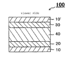
- FIG. 1 Schematic cross-sectional view of a liquid crystal panel according to a preferred embodiment of the present invention.
- FIG. 2 Schematic cross-sectional views illustrating an alignment state of liquid crystal molecules of a liquid crystal layer in a liquid crystal cell of a VA mode.
- FIG. 3 The results of a computer simulation regarding viewing angle dependence of a contrast of a liquid crystal panel produced in Example 1.
- FIG. 4 The results of a computer simulation regarding viewing angle dependence of a contrast of a liquid crystal panel produced in Example 2.
- FIG. 5 The results of a computer simulation regarding viewing angle dependence of a contrast of a liquid crystal panel produced in Example 3.
- FIG. 6 The results of a computer simulation regarding viewing angle dependence of a contrast of a liquid crystal panel produced in Example 4.
- FIG. 7 The results of a computer simulation regarding viewing angle dependence of a contrast of a liquid crystal panel produced in Example 5.
- FIG. 8 The results of a computer simulation regarding viewing angle dependence of a contrast of a liquid crystal panel produced in Comparative Example 1.
- FIG. 9 The results of a computer simulation regarding viewing angle dependence of a contrast of a liquid crystal panel produced in Comparative Example 2.
- FIG. 10 The results of a computer simulation regarding viewing angle dependence of a contrast of a liquid crystal panel produced in Comparative Example 3.
- nx refers to a refractive index in a direction providing a maximum in-plane refractive index (that is, a slow axis direction)
- the symbol “ny” refers to a refractive index in a direction perpendicular to the slow axis in the same plane (that is, a fast axis direction)
- the symbol “nz” refers to a refractive index in a thickness direction.
- in-plane retardation Re refers to an in-plane retardation value of a film (layer) measured at 23° C. by using light having a wavelength of 590 nm as far as not specified, particularly.
- Thickness direction retardation Rth refers to a thickness direction retardation value measured at 23° C. by using light of a wavelength of 590 nm as far as not specified, particularly.
- ⁇ Rth 1 to n in the above Expressions (1) and (2) represents the total thickness direction retardation from the first optical compensation layer to the n-th optical compensation layer.
- ⁇ Rth 1 to n Rth 1 +Rth 2 .
- ⁇ Rth 1 to n Rth 1 +Rth 2 +Rth 3 .
- ⁇ /2 plate refers to a plate having a function of converting linearly polarized light having a specific vibration direction into linearly polarized light having a vibration direction perpendicular thereto, or converting right-handed circularly polarized light into left-handed circularly polarized light (or converting left-handed circularly polarized light into right-handed circularly polarized light).
- the ⁇ /2 plate has an in-plane retardation value of a film (layer) of about 1 ⁇ 2 of a predetermined light wavelength (generally, in a visible light region).
- ⁇ /4 plate refers to a plate having a function of converting linearly polarized light of a specific wavelength into circularly polarized light (or converting circularly polarized light into linearly polarized light).
- the ⁇ /4 plate has an in-plane retardation value of a film (layer) of about 1 ⁇ 4 of a predetermined light wavelength (generally, in a visible light region).
- FIG. 1 is a schematic cross-sectional view of a liquid crystal panel according to a preferred embodiment of the present invention.
- a liquid crystal panel 100 includes a first polarizer 10 , a first optical compensation layer 20 , a liquid crystal cell 40 , a second optical compensation layer 30 , and a second polarizer 10 ′ in this order toward a viewer side.
- the first optical compensation layer 20 has a refractive index ellipsoid of nx>ny>nz and an in-plane retardation Re 1 of 90 to 300 nm.
- the second optical compensation layer 30 has a refractive index ellipsoid of nx>ny>nz and an in-plane retardation Re 2 of 90 to 300 nm.
- the total thickness direction retardation ⁇ Rth 1 to n of all the optical compensation layers and the thickness direction retardation Rth c of the liquid crystal cell satisfy the following Expression (1): ⁇ 160 nm ⁇ ( ⁇ Rth 1 to n ⁇ Rth c ) ⁇ 50 nm (1).
- any suitable pressure-sensitive adhesive layer or adhesive layer (not shown).
- any suitable protective film (not shown) is placed on a side of the first and second polarizers 10 and 10 ′ where the optical compensation layers are not formed. Further, if required, a protective film may be placed between the polarizer and the optical compensation layer.
- the first polarizer 10 and the second polarizer 10 ′ are typically placed so that the absorption axes thereof are perpendicular to each other.
- the absorption axis of the first polarizer is placed at an angle of 20° with respect to the horizontal direction of the liquid crystal panel.
- the absorption axis of the first polarizer is placed in parallel to the horizontal direction of the liquid crystal panel.
- the first optical compensation layer 20 is placed so that the slow axis thereof forms an angle of preferably 37° to 52°, more preferably 40° to 50°, particularly preferably 42° to 48°, and most preferably about 45° with respect to the absorption axis of the first polarizer 10 .
- the second optical compensation layer 30 is placed so that the slow axis thereof forms an angle of preferably ⁇ 37° to ⁇ 52°, more preferably ⁇ 40° to ⁇ 50°, particularly preferably ⁇ 42° to ⁇ 48°, and most preferably about ⁇ 45° with respect to the absorption axis of the first polarizer 10 .
- the second optical compensation layer 30 is placed so that the slow axis thereof is substantially perpendicular to the slow axis of the first optical compensation layer 20 .
- the respective polarizers and the respective optical compensation layers are placed with the above specific positional relationship, whereby a liquid crystal panel excellent in the balance between the contrast and the viewing angle properties is obtained.
- the term “substantially perpendicular” includes the case where an angle formed by two optical axes is 90° ⁇ 2°, and is preferably 90° ⁇ 1°. Further, in the specification of the present invention, for example, “45°” refers to an angle defined in a counterclockwise direction from a predetermined direction, and “ ⁇ 45°” refers to an angle defined in a clockwise direction from a predetermined direction.
- the difference between the total thickness direction retardation ⁇ Rth 1 to n of all the optical compensation layers and the thickness direction retardation Rth c of the liquid crystal cell in the liquid crystal panel of the present invention is larger than ⁇ 160 nm and smaller than 50 nm, and preferably larger than ⁇ 160 nm and smaller than 20 nm.
- Particular optical compensation layers are placed on both sides of the liquid crystal cell, and the relationship between the thickness direction retardation of the liquid crystal cell and the thickness direction retardations of the optical compensation layers is optimized, whereby a liquid crystal panel remarkably excellent in the balance between the contrast and the viewing angle properties is obtained.
- the difference between the total thickness direction retardation of the optical compensation layers and the thickness direction retardation of the liquid crystal cell is set in the above range, whereby a liquid crystal panel is obtained, in which a high contrast is obtained in a wide viewing angle range and the direction in which a high contrast is obtained is not so displaced from a front direction (ultimately, easily viewable for a viewer).
- the difference between the total thickness direction retardation of the optical compensation layers and the thickness direction retardation of the liquid crystal cell is preferably ⁇ 155 nm to ⁇ 70 nm, and more preferably ⁇ 140 nm to ⁇ 80 nm.
- the difference between the total thickness direction retardation of the optical compensation layers and the thickness direction retardation of the liquid crystal cell is preferably ⁇ 70 nm to 45 nm, more preferably ⁇ 70 nm to 20 nm, still more preferably ⁇ 70 nm to 10 nm, and particularly preferably ⁇ 60 nm to 10 nm.
- the difference is in the above range, a high contrast is obtained from a substantially front direction, which makes it very easy for a viewer to see a display screen image.
- the liquid crystal cell 40 includes a pair of glass substrates 41 , 41 ′, and a liquid crystal layer 42 as a display medium placed between the substrates.
- switching elements typically, TFTs
- scanning lines that provide a gate signal to the switching elements and signal lines that give a source signal thereto are provided (both of them are not shown).
- a color filter (not shown) is provided on the other substrate (color filter substrate) 41 ′.
- the color filter may be provided on the active matrix substrate 41 .
- the gap (cell gap) between the substrates 41 and 41 ′ is controlled with spacers (not shown).
- an alignment film (not shown) made of, for example, polyimide is provided.
- any appropriate drive mode may be employed for the drive mode of the liquid crystal cell 40 as long as the effects of the present invention may be obtained.
- the drive mode include a super twisted nematic (STN) mode, a twisted nematic (TN) mode, an in-plane switching (IPS) mode, a vertical alignment (VA) mode, an electrically controlled birefringence (ECB) mode, an optically aligned birefringence (OCB) mode, and a hybrid aligned nematic (HAN) mode.
- the VA mode, the ECB mode, and the OCB mode are preferred, because a liquid crystal panel excellent in the balance between the contract and the viewing angle properties may be obtained by using any liquid crystal cell of those modes in combination with the optical compensation layer to be used in the present invention.
- FIG. 2 is a schematic cross-sectional view illustrating an alignment state of liquid crystal molecules in a VA mode.
- liquid crystal molecules are aligned vertically to the substrates 41 , 41 ′ without application of a voltage.
- Such vertical alignment can be realized by arranging nematic liquid crystal having negative dielectric anisotropy between the substrates each having a vertical alignment film formed thereon (not shown).
- linear polarized light which passed through the polarizer 10 enters from a surface of one substrate 41 in such a state, the light enters the liquid crystal layer 42 , and the incident light advances along a longitudinal direction of the vertically aligned liquid crystal molecules.
- the thickness direction retardation Rth c of the liquid crystal cell is preferably 240 to 400 nm, more preferably 270 to 370 nm, and particularly preferably 300 to 340 nm.
- the first optical compensation layer has a refractive index ellipsoid of nx>ny>nz. That is, the first optical compensation layer is a biaxial retardation layer. Further, the in-plane retardation of the first optical compensation layer is 90 to 300 nm.
- the first optical compensation layer can function as a ⁇ /4 plate.
- the in-plane retardation Re 1 of the first optical compensation layer is preferably 90 to 180 nm, more preferably 100 to 160 nm, and still more preferably 110 to 150 nm.
- the optical compensation for the liquid crystal cell may be performed appropriately by setting the in-plane retardation value in the above range, and hence a liquid crystal panel may be obtained, which is excellent in the balance between the contrast and the viewing angle properties and has a high contrast ratio in an oblique direction.
- the thickness direction retardation Rth 1 of the first optical compensation layer is preferably 80 to 190 nm, more preferably 80 to 165 nm, and still more preferably 80 to 160 nm. In another embodiment, the thickness direction retardation Rth 1 of the first optical compensation layer is preferably 100 to 390 nm, more preferably 120 to 370 nm, and still more preferably 150 to 350 nm.
- the optical compensation for the liquid crystal cell is performed appropriately by setting the thickness direction retardation value in the above range, and hence a liquid crystal panel that is excellent in the balance between the contrast and the viewing angle properties and has a high contrast ratio in an oblique direction may be obtained.
- the Nz coefficient of the first optical compensation layer is preferably more than 1.05, more preferably 1.1 or more, and still more preferably 1.15 or more. Further, the Nz coefficient is preferably 2.15 or less, more preferably less than 1.9, still more preferably 1.8 or less, and particularly preferably 1.75 or less. When the Nz coefficient is in the above range, the viewing angle properties may be enhanced.
- the first optical compensation layer may be formed of any suitable material.
- the first optical compensation layer may be, for example, a polymer film or a coating film.
- the polymer film may be a film obtained by forming a resin such as a polycarbonate-based resin, a norbornene-based resin, a cellulose-based resin, a polyvinyl alcohol-based resin, or a polysulfone-based resin by any suitable forming method. They may be used alone or in combination. Of those, a film obtained by forming a polycarbonate-based resin or a norbornene-based resin by solvent casting method, melt extrusion, or the like may be used preferably. This is because a polymer film excellent in smoothness and optical uniformity may be obtained.
- a resin such as a polycarbonate-based resin, a norbornene-based resin, a cellulose-based resin, a polyvinyl alcohol-based resin, or a polysulfone-based resin by any suitable forming method. They may be used alone or in combination. Of those, a film obtained by forming a polycarbonate-based resin or a norbornene-based resin by solvent casting method
- an aromatic polycarbonate is preferably used.
- the aromatic polycarbonate can be typically obtained by the reaction between a carbonate precursor and an aromatic dihydric phenol compound.
- Specific examples of the carbonate precursor include phosgene, bischloroformate of dihydric phenols, diphenyl carbonate, di-p-tolylcarbonate, phenyl-p-tolylcarbonate, di-p-chlrophenylcarbonate, and dinaphthylcarbonate. Of those, phosgene and diphenylcarbonate are preferred.
- aromatic dihydric phenol compound examples include: 2,2-bis(4-hydroxyphenyl)propane; 2,2-bis(4-hydroxy-3,5-dimethylphenyl)propane; bis(4-hydroxyphenyl)methane; 1,1-bis(4-hydroxyphenyl)ethane; 2,2-bis(4-hydroxyphenyl)butane; 2,2-bis(4-hydroxy-3,5-dimethylphenyl)butane; 2,2-bis(4-hydroxy-3,5-dipropylphenyl)propane; 1,1-bis(4-hydroxyphenyl)cyclohexane; and 1,1-bis(4-hydroxyphenyl)-3,3,5-trimethylcyclohexane.
- 2,2-bis(4-hydroxyphenyl)propane 1,1-bis(4-hydroxyphenyl)cyclohexane
- 1,1-bis(4-hydroxyphenyl)-3,3,5-trimethylcyclohexane 2,2-bis(4-hydroxyphenyl)propane and 1,1-bis(4-hydroxyphenyl)-3,3,5-trimethylcyclohexane are preferably used in combination.
- the above norbornene-based resin is obtained by polymerizing a norbornene-based monomer as a polymerization unit.
- the norbornene-based monomer include: norbornene, and its alkyl and/or alkylidene-substituted monomers such as 5-methyl-2-norbornene, 5-dimethyl-2-norbornene, 5-ethyl-2-norbornene, 5-butyl-2-norbornene, 5-ethylidene-2-norbornene, and substituted monomers of norbornene and its alkyl and/or alkylidene-substituted monomers with a polar group such as halogen; dicyclopentadiene, 2,3-dihydrodicyclopentadiene, or the like; dimethanooctahydronaphthalene, its substituted monomers with alkyl and/or alkylidene, and its substituted monomers with a polar group such as
- the above polymer film may further contain any suitable additive.
- the additive include a plasticizer, a thermal stabilizer, a light stabilizer, a lubricant, an antioxidant, a UV absorber, a flame retardant, a colorant, an antistatic agent, a compatibilizing agent, a cross-linking agent, and a thickener.
- the content of the additive is preferably more than 0 to 10 or less parts by weight with respect to 100 parts by weight of the above resin.
- Any suitable commercially-available product may be used as the above polymer film.
- the above coating film may be formed of a resin such as a polyamide-based resin, a polyimide-based resin, a polyester-based resin, a polyether ketone-based resin, a polyamide imide-based resin, or a polyester imide-based resin.
- a resin such as a polyamide-based resin, a polyimide-based resin, a polyester-based resin, a polyether ketone-based resin, a polyamide imide-based resin, or a polyester imide-based resin.
- Those resins may be used alone, or may be used as a mixture of two or more kinds of resins having different functional groups, for example, as a mixture of polyaryletherketone and polyamide.
- the polyimide-based resin may be preferably used in view of its high transparency, high aligning property, and high stretching property.
- resins that can form the above coating film may include those resins described in JP 2006-317495 A.
- the coating film can further contain any suitable additive.
- the additive and the content thereof are similar to those which may be contained in the polymer film.
- An example of the method of forming a coating film from the resin includes a method of applying a solution of the resin to any suitable base film and removing a solvent from the solution.
- a specific example of the method includes a method described in JP 2006-317495 A.
- a first optical compensation layer having the above-mentioned optical properties may be formed by stretching the polymer film or the coating film.
- the stretching conditions may be selected appropriately depending upon a material for forming the polymer film or the coating film, the thickness of the polymer film or the coating film, the optical properties desired for the first optical compensation layer, and the like.
- the stretching temperature is preferably 130 to 170° C. and more preferably 135 to 165° C.
- the stretching ratio is, for example, 1.1 to 2.8 times, preferably 1.2 to 2.8 times, and more preferably 1.3 to 2.5 times.
- An example of the stretching method includes transverse uniaxial stretching (fixed-end biaxial stretching).
- the thickness of the first optical compensation layer is typically 20 to 80 ⁇ m, preferably 30 to 70 ⁇ m, and more preferably 40 to 60 ⁇ m.
- the coating film contains a polyimide-based resin
- a method of stretching or shrinking the base film and the coating film formed on the base film together may be typically used.
- stretching or shrinking is performed at a predetermined heating temperature.
- the heating temperature is, for example, 130 to 170° C.
- the stretching ratio is, for example, 1.3 to 2.5 times and preferably 1.5 to 2.0 times.
- An example of the stretching method includes transverse uniaxial stretching (fixed-end biaxial stretching).
- the thickness of the first optical compensation layer is typically 0.1 to 10 ⁇ m, preferably 0.5 to 8 ⁇ m, and more preferably 1 to 5 ⁇ m.
- the first optical compensation layer 20 is placed between the first polarizer 10 and the liquid crystal cell 40 .
- any suitable method may be adopted depending upon the purpose.
- a pressure-sensitive adhesive layer (not shown) is provided on the liquid crystal cell 40 side of the first optical compensation layer 20 and the first optical compensation layer 20 is attached to the liquid crystal cell.
- a pressure-sensitive adhesive layer (not shown) is provided on the first polarizer 10 side of the first optical compensation layer 20 , and the first polarizer 10 is attached to the first optical compensation layer 20 .
- the first polarizer 10 and the first optical compensation layer 20 may be attached to each other to form a laminate, and then the laminate may be attached to the liquid crystal cell.
- the second optical compensation layer has a refractive index ellipsoid of nx>ny>nz and an in-plane retardation Re 2 of 90 to 300 nm.
- the details of the second optical compensation layer such as the optical properties thereof, the materials for forming thereof, and the method of forming thereof are as described in the section C regarding the first optical compensation layer, and hence the descriptions thereof is omitted.
- the thickness direction retardation Rth 2 of the second optical compensation layer is 80 to 190 nm, preferably 80 to 165 nm, and more preferably 80 to 160 nm.
- the second optical compensation layer is formed of the same material as that for the first optical compensation layer, and has the same thickness as that of the first optical compensation layer.
- the second optical compensation layer 30 is placed between the second polarizer 10 ′ and the liquid crystal cell 40 .
- the same method as that of placing the first optical compensation layer may be used.
- any suitable polarizers may be employed depending on the purpose.
- the polarizer include: a film prepared by adsorbing a dichromatic substance such as iodine or a dichromatic dye on a hydrophilic polymer film such as a polyvinyl alcohol-based film, a partially formalized polyvinyl alcohol-based film, or an ethylene/vinyl acetate copolymer-based partially saponified film and uniaxially stretching the film; and a polyene-based orientated film such as a dehydrated product of a polyvinyl alcohol-based film or a dechlorinated product of a polyvinyl chloride-based film.
- a polarizer prepared by adsorbing a dichromatic substance such as iodine on a polyvinyl alcohol-based film and uniaxially stretching the film is particularly preferred in view of high polarized dichromaticity.
- a thickness of the polarizer is not particularly limited, but is generally about 1 to 80 ⁇ m.
- the first polarizer 10 and the second polarizer 10 ′ may be identical or different.
- the polarizer prepared by adsorbing iodine on a polyvinyl alcohol-based film and uniaxially stretching the film may be produced by, for example: immersing a polyvinyl alcohol-based film in an aqueous solution of iodine for coloring; and stretching the film to a 3 to 7 times length of the original length.
- the aqueous solution may contain boric acid, zinc sulfate, zinc chloride, or the like as required, or the polyvinyl alcohol-based film may be immersed in an aqueous solution of potassium iodide or the like. Further, the polyvinyl alcohol-based film may be immersed and washed in water before coloring as required.
- washing the polyvinyl alcohol-based film with water not only allows removal of contamination on a film surface or washing away of an antiblocking agent, but also prevents nonuniformity such as uneven coloring or the like by swelling the polyvinyl alcohol-based film.
- the stretching of the film may be carried out after coloring of the film with iodine, carried out during coloring of the film, or carried out followed by coloring of the film with iodine.
- the stretching may be carried out in an aqueous solution of boric acid or potassium iodide, or in a water bath.
- any appropriate film which can be used as a protective film of a polarizing plate may be employed.
- a material used as a main component of the film include transparent resins such as a cellulose-based resin such as triacetylcellulose (TAC), a polyester-based resin, a polyvinyl alcohol-based resin, a polycarbonate-based resin, a polyamide-based resin, a polyimide-based resin, a polyether sulfone-based resin, a polysulfone-based resin, a polystyrene-based resin, a polynorbornene-based resin, a polyolefin-based resin, an acrylic resin, and an acetate-based resin.
- TAC triacetylcellulose
- Another example thereof includes an acrylic, urethane-based, acrylic urethane-based, epoxy-based, or silicone-based thermosetting resin or UV-curing resin. Still another example thereof includes a glassy polymer such as a siloxane-based polymer. Further, a polymer film described in JP 2001-343529 A (WO 01/37007) may also be used. To be specific, the film is formed of a resin composition containing a thermoplastic resin having a substituted or unsubstituted imide group on a side chain, and a thermoplastic resin having a substituted or unsubstituted phenyl group and a nitrile group on a side chain.
- a specific example thereof includes a resin composition containing an alternate copolymer of isobutene and N-methylmaleimide, and an acrylonitrile/styrene copolymer.
- the polymer film may be an extruded product of the above-mentioned resin composition, for example.
- TAC a polyimide-based resin, a polyvinyl alcohol-based resin, and a glassy polymer are preferable, and TAC is more preferable.
- the protective film be transparent and have no color. Further, it is preferable that the protective film provided between a polarizer and an optical compensation layer substantially has optical isotropy. In one embodiment, the protective film provided between a polarizer and an optical compensation layer has an in-plane retardation of 0 to 10 nm and a thickness direction retardation of 0 to 10 nm.
- the thickness of the protective film is preferably 5 mm or less, more preferably 1 mm or less, particularly preferable 1 to 500 ⁇ m, and most preferably 5 to 150 ⁇ m.
- the protective film provided on the outer side of the polarizers 10 and 10 ′ may be subjected to hard coat treatment, antireflection treatment, anti-sticking treatment, anti-glare treatment, or the like as required.
- any appropriate pressure-sensitive adhesive can be adopted.
- a solvent type pressure-sensitive adhesive a non-aqueous emulsion type pressure-sensitive adhesive, an aqueous pressure-sensitive adhesive, and a hotmelt pressure-sensitive adhesive.
- a solvent type pressure-sensitive adhesive containing an acrylic polymer as a base polymer is preferably used.
- the thickness of the above pressure-sensitive adhesive layer can be appropriately set depending upon the use purpose, the adhesion strength, and the like. Specifically, the thickness of the pressure-sensitive adhesive layer is preferably 1 ⁇ m to 100 ⁇ m, more preferably 5 ⁇ m to 50 ⁇ m, and still more preferably 10 ⁇ m to 30 ⁇ m.
- an adhesive forming an adhesive layer typically, there is a curable adhesive.
- the curable adhesive include a photo-curable adhesive such as a UV-curable adhesive, a moisture-curable adhesive, and a thermosetting adhesive.
- the applying amount of an adhesive between respective layers can be set appropriately depending upon the purpose.
- the applying amount is preferably 0.3 to 3 ml, more preferably 0.5 to 2 ml, and still more preferably 1 to 2 ml per area (cm 2 ) with respect to a principal plane of each layer.
- the thickness of the adhesive layer thus obtained is preferably 0.1 to 20 ⁇ m, more preferably 0.5 to 15 ⁇ m, and still more preferably 1 to 10 ⁇ M.
- the above pressure-sensitive adhesive or adhesive can be selected appropriately depending upon the kind of an adherend (optical element).
- the liquid crystal panel of the present invention may further include another optical element.
- another optical element any suitable optical element may be adopted depending upon the purpose and the kind of the liquid crystal panel. Specific examples thereof include a liquid crystal film, a light scattering film, a diffraction film, and another optical compensation layer (retardation film).
- Each of the optical elements in the liquid crystal panel of the present invention may be subjected to treatment with a UV absorbing agent such as a salicylic ester-based compound, a benzophenone-based compound, a benzotriazole-based compound, a cyanoacrylate-based compound, or a nickel complex salt-based compound, to thereby impart UV absorbing property.
- a UV absorbing agent such as a salicylic ester-based compound, a benzophenone-based compound, a benzotriazole-based compound, a cyanoacrylate-based compound, or a nickel complex salt-based compound
- the liquid crystal panel of the present invention may be also applied preferably to any of transmission-type, reflection-type, and semi-transmission-type liquid crystal display apparatuses.
- a transmission-type liquid crystal display apparatus a brightness enhancement film, a prism sheet, a light guide plate, a backlight, and the like are provided on a reverse side (opposite side of the viewer side) of the liquid crystal panel of the present invention.
- the liquid crystal display apparatus including the liquid crystal display panel of the present invention include a personal computer, a liquid crystal television, a mobile telephone, and a personal digital assistant (PDA).
- PDA personal digital assistant
- the thicknesses of polarizing plates each with an optical compensation layer in examples and comparative examples were measured using DIAL GAUGE manufactured by Ozaki Mfg. Co. Ltd.
- a computer simulation was conducted regarding the liquid crystal panels in the respective examples and comparative examples, using the optical properties parameters of the respective optical compensation layers produced and measured actually.
- a simulator for a liquid crystal display unit “LCD MASTER” manufactured by SHINTEC Co., Ltd. was used.
- the values of the in-plane retardation and the thickness direction retardation at a wavelength of 590 nm and 23° C. were measured using a retardation measurement apparatus “KOBRA21-ADH” (trade name) manufactured by Oji Scientific Instruments) employing a parallel Nicols rotation method as a principle.
- a VA-mode liquid crystal cell mounted on Play Station Portable (PSP) (trade name) manufactured by Sony Corporation was used.
- the thickness direction retardation Rth c of the liquid crystal cell was 320 nm.
- a commercially-available polyvinyl alcohol film (manufactured by Kurary Co., Ltd.) was dyed in an aqueous solution containing iodine, and uniaxially stretched by 6 times between rolls having different velocities in an aqueous solution containing boric acid to thereby obtain a polarizer.
- Triacetylcellulose films (thickness: 40 ⁇ m, KC4UYW (tradename) manufactured by Konica Minolta Opto, Inc.), as protective films, were attached on both surfaces of the polarizer with a polyvinyl alcohol-based adhesive (thickness: 0.1 ⁇ m), whereby a polarizing plate was obtained.
- the in-plane retardation Re (550) of the protective film was 0.9 nm.
- Re (550) represents a value measured with light having a wavelength of 550 nm at 23° C.
- a long-shaped norbornene-based resin film (Zeonor (tradename) manufactured by Nippon Zeon Co., Ltd., thickness: 60 ⁇ m, photoelastic coefficient: 3.1 ⁇ 10 ⁇ 12 m 2 /N) was subjected to fixed-end biaxial stretching by 1.85 times at 150° C., whereby a long-shaped film was produced.
- the film thus obtained was punched to a size corresponding to the liquid crystal cell to obtain a first optical compensation layer.
- the obtained film had a refractive index ellipsoid of nx>ny>nz, an in-plane retardation Re 1 of 140 nm, a thickness direction retardation Rth 1 of 84 nm, and an Nz coefficient of 1.1.
- a second optical compensation layer (Re 2 : 140 nm, Rth 2 : 84 nm, Nz coefficient: 1.1) was obtained in the same way as in the first optical compensation layer.
- the polarizing plate and the second optical compensation layer obtained as described above were laminated via an acrylic pressure-sensitive adhesive (thickness: 12 ⁇ m), whereby a laminated film A was produced.
- the polarizing plate and the second optical compensation layer were laminated so that the slow axis of the second optical compensation layer formed an angle of 45° with respect to the absorption axis of the polarizer of the polarizing plate.
- the polarizing plate and the first optical compensation layer obtained as described above were laminated via an acrylic pressure-sensitive adhesive (thickness: 12 ⁇ m), where by a laminated film B was produced.
- the polarizing plate and the first optical compensation layer were laminated so that the slow axis of the first optical compensation layer formed an angle of 45° with respect to the absorption axis of the polarizer of the polarizing plate.
- the laminated film A was attached to the viewer side of the liquid crystal cell removed from the PSP via an acrylic pressure-sensitive adhesive (thickness: 20 ⁇ m). At this time, the laminated film A was attached so that the second optical compensation layer was placed on the liquid crystal cell side.
- the laminated film B was attached to the backlight side of the liquid crystal cell via an acrylic pressure-sensitive adhesive (thickness: 20 ⁇ m). At this time, the laminated film B was attached so that the first optical compensation layer was placed on the liquid crystal cell side. Further, the lamination was performed so that the absorption axis of the polarizer of the laminated film A and the absorption axis of the polarizer of the laminated film B were substantially perpendicular to each other.
- the lamination was performed so that the slow axis of the first optical compensation layer formed an angle of 45°, the slow axis of the second optical compensation layer formed an angle of 135°, and the absorption axis of the polarizer on the viewer side formed an angle of 90° in a counterclockwise direction with respect to the absorption axis of the polarizer on the backlight side as the standard (0°).
- a liquid crystal panel was obtained.
- FIG. 3 shows the results. Note that the difference between the total thickness direction retardation ⁇ Rth 1 to 2 of all the optical compensation layers in the liquid crystal panel and the thickness direction retardation Rth c of the liquid crystal cell was ⁇ 152 nm.
- a liquid crystal panel was produced in the same way as in Example 1 except that the stretching ratio of the film was set to be 1.75 times when producing the first and second optical compensation layers.
- the first and second optical compensation layers each had a refractive index ellipsoid of nx>ny>nz, an in-plane retardation Re of 140 nm, a thickness direction retardation Rth of 91 nm, and an Nz coefficient of 1.15.
- FIG. 4 shows the results. Note that the difference between the total thickness direction retardation ⁇ Rth 1 to 2 of all the optical compensation layers in the liquid crystal panel and the thickness direction retardation Rth c of the liquid crystal cell was ⁇ 138 nm.
- a liquid crystal panel was produced in the same way as in Example 1 except that the stretching ratio of the film was set to be 1.5 times when producing the first and second optical compensation layers.
- the first and second optical compensation layers each had a refractive index ellipsoid of nx>ny>nz, an in-plane retardation Re of 140 nm, a thickness direction retardation Rth of 112 nm, and an Nz coefficient of 1.3.
- FIG. 5 shows the results. Note that the difference between the total thickness direction retardation ⁇ Rth 1 to 2 of all the optical compensation layers in the liquid crystal panel and the thickness direction retardation Rth c of the liquid crystal cell was ⁇ 96 nm.
- a liquid crystal panel was produced in the same way as in Example 1 except that the stretching ratio of the film was set to be 1.3 times when producing the first and second optical compensation layers.
- the first and second optical compensation layers each had a refractive index ellipsoid of nx>ny>nz, an in-plane retardation Re of 140 nm, a thickness direction retardation Rth of 140 nm, and an Nz coefficient of 1.5.
- FIG. 6 shows the results. Note that the difference between the total thickness direction retardation ⁇ Rth 1 to 2 of all the optical compensation layers in the liquid crystal panel and the thickness direction retardation Rth c of the liquid crystal cell was ⁇ 40 nm.
- a liquid crystal panel was produced in the same way as in Example 1 except that the stretching ratio of the film was set to be 1.15 times when producing the first and second optical compensation layers.
- the first and second optical compensation layers each had a refractive index ellipsoid of nx>ny>nz, an in-plane retardation Re of 140 nm, a thickness direction retardation Rth of 182 nm, and an Nz coefficient of 1.8.
- FIG. 7 shows the results. Note that the difference between the total thickness direction retardation ⁇ Rth 1 to 2 of all the optical compensation layers in the liquid crystal panel and the thickness direction retardation Rth c of the liquid crystal cell was 44 nm.
- a liquid crystal panel was produced in the same way as in Example 1 except that the stretching ratio of the film was set to be 2 times when producing the first and second optical compensation layers.
- the first and second optical compensation layers each had a refractive index ellipsoid of nx>ny>nz, an in-plane retardation Re of 140 nm, a thickness direction retardation Rth of 77 nm, and an Nz coefficient of 1.05.
- FIG. 8 shows the results. Note that the difference between the total thickness direction retardation ⁇ Rth 1 to 2 of all the optical compensation layers in the liquid crystal panel and the thickness direction retardation Rth c of the liquid crystal cell was ⁇ 166 nm.
- a liquid crystal panel was produced in the same way as in Example 1 except that the stretching ratio of the film was set to be 1.05 times when producing the first and second optical compensation layers.
- the first and second optical compensation layers each had a refractive index ellipsoid of nx>ny>nz, an in-plane retardation Re of 140 nm, a thickness direction retardation Rth of 196 nm, and an Nz coefficient of 1.9.
- FIG. 9 shows the results. Note that the difference between the total thickness direction retardation ⁇ Rth 1 to 2 of all the optical compensation layers in the liquid crystal panel and the thickness direction retardation Rth c of the liquid crystal cell was 72 nm.
- a liquid crystal panel was produced in the same way as in Example 1 except that the stretching ratio of the film was set to be 1.02 times when producing the first and second optical compensation layers.
- the first and second optical compensation layers each had a refractive index ellipsoid of nx>ny>nz, an in-plane retardation Re of 140 nm, a thickness direction retardation Rth of 210 nm, and an Nz coefficient of 2.0.
- FIG. 10 shows the results. Note that the difference between the total thickness direction retardation ⁇ Rth 1 to 2 of all the optical compensation layers in the liquid crystal panel and the thickness direction retardation Rth c of the liquid crystal cell was 100 nm.
- FIGS. 3 to 10 are contrast contour maps.
- the contours in FIGS. 3 to 6 and 8 to 10 are 100 , 50 , 30 , 20 , and 10 in the stated order from the center, and the contours in FIG. 7 are 50 , 40 , 30 , 20 , and 10 in the stated order from the center.
- the liquid crystal panel to be obtained has a remarkably excellent balance between the contrast and the viewing angle properties.
- the liquid crystal panel and the liquid crystal display apparatus of the present invention may preferably be applied to a personal computer, a liquid crystal television, a mobile telephone, a personal digital assistant (PDA), etc.
- a personal computer a liquid crystal television, a mobile telephone, a personal digital assistant (PDA), etc.
- PDA personal digital assistant
Abstract
Description
- Patent Document 1: JP 11-242226 A
- Patent Document 2: JP 2001-209065 A
−160 nm<(ΣRth 1 to n −Rth c)<50 nm (1).
−160 nm<(ΣRth 1 to n −Rth c)<20 nm (2).
- 100 liquid crystal panel
- 10 first polarizer
- 20 first optical compensation layer
- 30 second optical compensation layer
- 40 liquid crystal cell
- 10′ second polarizer
- 41, 41′ substrate
- 42 liquid crystal layer
ΣRth 1 to n =Rth 1 +Rth 2.
When the liquid crystal panel of the present invention further includes a third optical compensation layer, ΣRth1 to n is expressed as follows:
ΣRth 1 to n =Rth 1 +Rth 2 +Rth 3.
−160 nm<(ΣRth 1 to n −Rth c)<50 nm (1).
Claims (7)
−160 nm<(ΣRth 1 to n −Rth c)<50 nm (1).
−160 nm<(ΣRth 1 to n −Rth c)<20 nm (2).
Applications Claiming Priority (3)
| Application Number | Priority Date | Filing Date | Title |
|---|---|---|---|
| JP2006-347714 | 2006-12-25 | ||
| JP2006347714 | 2006-12-25 | ||
| PCT/JP2007/073378 WO2008078514A1 (en) | 2006-12-25 | 2007-12-04 | Liquid crystal panel and liquid crystal display apparatus utilizing the same |
Publications (2)
| Publication Number | Publication Date |
|---|---|
| US20090268137A1 US20090268137A1 (en) | 2009-10-29 |
| US8072567B2 true US8072567B2 (en) | 2011-12-06 |
Family
ID=39562308
Family Applications (1)
| Application Number | Title | Priority Date | Filing Date |
|---|---|---|---|
| US12/519,036 Expired - Fee Related US8072567B2 (en) | 2006-12-25 | 2007-12-04 | Liquid crystal panel and liquid crystal display apparatus using the same |
Country Status (4)
| Country | Link |
|---|---|
| US (1) | US8072567B2 (en) |
| JP (1) | JP2008181082A (en) |
| KR (1) | KR20090080136A (en) |
| WO (1) | WO2008078514A1 (en) |
Families Citing this family (6)
| Publication number | Priority date | Publication date | Assignee | Title |
|---|---|---|---|---|
| JP5364343B2 (en) * | 2008-11-10 | 2013-12-11 | スタンレー電気株式会社 | Liquid crystal display |
| JP2010128094A (en) * | 2008-11-26 | 2010-06-10 | Stanley Electric Co Ltd | Liquid crystal display element and method of manufacturing the same |
| JP5239967B2 (en) * | 2009-03-17 | 2013-07-17 | 住友化学株式会社 | Liquid crystal display and polarizing plate set |
| JP5511457B2 (en) * | 2010-03-23 | 2014-06-04 | スタンレー電気株式会社 | Liquid crystal display |
| JP2013015815A (en) * | 2011-06-06 | 2013-01-24 | Seiko Epson Corp | Projection type display device and optical unit |
| KR20190008020A (en) * | 2017-07-14 | 2019-01-23 | 삼성전자주식회사 | Liquid crystal display |
Citations (39)
| Publication number | Priority date | Publication date | Assignee | Title |
|---|---|---|---|---|
| JPH09325212A (en) | 1996-05-31 | 1997-12-16 | Sumitomo Chem Co Ltd | Optically anisotropic film and liquid crystal display |
| JPH1068816A (en) | 1996-08-29 | 1998-03-10 | Sharp Corp | Phase difference plate and circularly polarizing plate |
| JPH11242226A (en) | 1997-12-26 | 1999-09-07 | Sharp Corp | Liquid crystal display device |
| JP2000227520A (en) | 1999-02-08 | 2000-08-15 | Nitto Denko Corp | Phase difference plate, laminated polarizing plate and liquid crystal display device |
| JP3174367B2 (en) | 1991-10-07 | 2001-06-11 | 日東電工株式会社 | Laminated wave plate and circularly polarizing plate |
| US20010007487A1 (en) | 1999-11-01 | 2001-07-12 | Yea-Sun Yoon | Liquid crystal display having wide viewing angle |
| JP2001209065A (en) | 1999-12-02 | 2001-08-03 | Samsung Electronics Co Ltd | Liquid crystal display device with wide viewing angle and substrate to be used for the same |
| US20010048497A1 (en) | 2000-05-31 | 2001-12-06 | Koichi Miyachi | Liquid crystal display apparatus |
| US20020047968A1 (en) * | 2000-08-28 | 2002-04-25 | Keisuke Yoshida | Liquid crystal display device |
| JP2003075635A (en) | 2001-09-04 | 2003-03-12 | Nitto Denko Corp | Optical film, polarizing plate and display device |
| US6717637B1 (en) | 1998-10-30 | 2004-04-06 | Samsung Electronics Co., Ltd. | Liquid crystal display having wide viewing angle |
| US20040183973A1 (en) * | 2003-02-12 | 2004-09-23 | 3M Innovative Properties Company | Compensators for liquid crystal displays |
| JP2004326089A (en) | 2003-04-07 | 2004-11-18 | Dainippon Printing Co Ltd | Laminated phase difference layer, its manufacturing method and liquid crystal display device using phase difference layer |
| US20040252264A1 (en) * | 2003-03-28 | 2004-12-16 | Sumitomo Chemical Company, Limited | Polarizer having retarder and liquid crystal display apparatus comprising the same |
| US20050062917A1 (en) | 2003-04-07 | 2005-03-24 | Keiji Kashima | Laminated retardation layer, its fabrication process, and liquid crystal display incorporating the same |
| US20050112299A1 (en) * | 2001-03-01 | 2005-05-26 | Konica Corporation | Cellulose ester film, its manufacturing method, polarizing plate, and liquid crystal display |
| US20050140900A1 (en) | 2003-10-22 | 2005-06-30 | Lg Chem, Ltd. | In-plane switching liquid crystal display comprising compensation film for angular field of view using +A-plate and +C-plate |
| CN1683972A (en) | 2004-04-16 | 2005-10-19 | 夏普株式会社 | Circularly polarizing plate and liquid crystal display device |
| US20050243248A1 (en) | 1998-10-30 | 2005-11-03 | Yea-Sun Yoon | Liquid crystal display having wide viewing angle |
| US20060007375A1 (en) * | 2004-06-24 | 2006-01-12 | Sumitomo Chemical Company, Limited | Phase retarder, a laminate polarizing plate a method for producing thereof, and a liquid crystal display |
| US20060062934A1 (en) * | 2004-08-26 | 2006-03-23 | Nitto Denko Corporation | Retardation film and method of producing the same, and optical film, liquid crystal panel, and liquid crystal display apparatus all using the retardation film |
| WO2006059545A1 (en) | 2004-12-02 | 2006-06-08 | Nitto Denko Corporation | Polarizing plate with optical compensation layer and image display employing same |
| JP2006154436A (en) | 2004-11-30 | 2006-06-15 | Sharp Corp | Liquid crystal display apparatus and circularly polarizing film |
| JP2006195441A (en) | 2004-12-16 | 2006-07-27 | Nitto Denko Corp | Liquid crystal display |
| JP2006215221A (en) | 2005-02-03 | 2006-08-17 | Nitto Denko Corp | Polarizing element, liquid crystal panel, liquid crystal television, liquid crystal display device, and method for manufacturing polarizing element |
| US20060203162A1 (en) * | 2005-03-08 | 2006-09-14 | Hideki Ito | Liquid crystal display device |
| US7126754B2 (en) * | 2002-06-18 | 2006-10-24 | Nitto Denko Corporation | Polarization plate with optical compensation layer and image display device |
| JP2006309130A (en) | 2004-12-02 | 2006-11-09 | Nitto Denko Corp | Polarizing plate with optical compensating layer, and image display using the same |
| JP2007286578A (en) | 2006-03-23 | 2007-11-01 | Fujifilm Corp | Optical-compensation film incorporating polarizing plate and liquid crystal display device |
| JP2008129175A (en) | 2006-11-17 | 2008-06-05 | Nippon Oil Corp | Elliptical polarizing plate and vertically aligned liquid crystal display apparatus using the same |
| US7462381B2 (en) * | 2002-04-26 | 2008-12-09 | Nitto Denko Corporation | Method for producing birefringent film |
| US20090040443A1 (en) * | 2005-11-25 | 2009-02-12 | Nitto Denko Corporation | Method of producing a liquid crystal panel, liquid crystal panel, and image display apparatus |
| US7522238B2 (en) * | 2004-04-26 | 2009-04-21 | Sumitomo Chemical Company, Limited | Laminate polarizing plate, a method of producing the same and a liquid crystal display |
| US7557883B2 (en) * | 2006-07-12 | 2009-07-07 | Nitto Denko Corporation | Polarizing plate with optical compensation layer, method of producing the same, and liquid crystal panel, liquid crystal display, and image display including the same |
| US7630038B2 (en) * | 2005-11-10 | 2009-12-08 | Nitto Denko Cororation | Liquid crystal panel and liquid crystal display apparatus |
| US20100026936A1 (en) | 2006-11-17 | 2010-02-04 | Nippon Oil Corporation | Elliptical Polarizer and Vertical Alignment Type Liquid Crystal Display Device Comprising the Same |
| US7695780B2 (en) * | 2004-02-26 | 2010-04-13 | Fujifilm Corporation | Optical film, optical compensation sheet, polarizing plate, and liquid crystal display device |
| US7738065B2 (en) * | 2005-05-11 | 2010-06-15 | Nitto Denko Corporation | Polarizing plate provided with optical compensation layers and image display apparatus using the same |
| US8018556B2 (en) * | 2007-10-04 | 2011-09-13 | Nec Lcd Technologies, Ltd | Liquid crystal display device having a biaxial first anisotropic film and a second anisotropic film having an optical axis in a thickness direction |
-
2007
- 2007-11-20 JP JP2007300075A patent/JP2008181082A/en active Pending
- 2007-12-04 KR KR1020097012443A patent/KR20090080136A/en not_active Application Discontinuation
- 2007-12-04 US US12/519,036 patent/US8072567B2/en not_active Expired - Fee Related
- 2007-12-04 WO PCT/JP2007/073378 patent/WO2008078514A1/en active Application Filing
Patent Citations (60)
| Publication number | Priority date | Publication date | Assignee | Title |
|---|---|---|---|---|
| JP3174367B2 (en) | 1991-10-07 | 2001-06-11 | 日東電工株式会社 | Laminated wave plate and circularly polarizing plate |
| JPH09325212A (en) | 1996-05-31 | 1997-12-16 | Sumitomo Chem Co Ltd | Optically anisotropic film and liquid crystal display |
| JPH1068816A (en) | 1996-08-29 | 1998-03-10 | Sharp Corp | Phase difference plate and circularly polarizing plate |
| US7394511B2 (en) | 1997-12-26 | 2008-07-01 | Sharp Kabushiki Kaisha | Liquid crystal display |
| US20080170186A1 (en) | 1997-12-26 | 2008-07-17 | Masayuki Okamoto | Liquid crystal display |
| US6900863B2 (en) | 1997-12-26 | 2005-05-31 | Sharp Kabushiki Kaisha | Liquid crystal display |
| US20040160537A1 (en) | 1997-12-26 | 2004-08-19 | Sharp Kabushiki Kaisha | Liquid crystal display |
| US6281952B1 (en) | 1997-12-26 | 2001-08-28 | Sharp Kabushiki Kaisha | Liquid crystal display |
| JPH11242226A (en) | 1997-12-26 | 1999-09-07 | Sharp Corp | Liquid crystal display device |
| US20010052948A1 (en) | 1997-12-26 | 2001-12-20 | Sharp Kabushiki Kaisha | Liquid crystal display |
| US6563554B2 (en) | 1997-12-26 | 2003-05-13 | Sharp Kabushiki Kaisha | Liquid crystal display |
| US20060119752A1 (en) | 1997-12-26 | 2006-06-08 | Masayuki Okamoto | Liquid crystal display |
| US7050132B2 (en) | 1997-12-26 | 2006-05-23 | Sharp Kabushiki Kaisha | Liquid crystal display |
| US20030067570A1 (en) | 1997-12-26 | 2003-04-10 | Sharp Kabushiki Kaisha | Liquid crystal display |
| US6717637B1 (en) | 1998-10-30 | 2004-04-06 | Samsung Electronics Co., Ltd. | Liquid crystal display having wide viewing angle |
| US20050243248A1 (en) | 1998-10-30 | 2005-11-03 | Yea-Sun Yoon | Liquid crystal display having wide viewing angle |
| JP2000227520A (en) | 1999-02-08 | 2000-08-15 | Nitto Denko Corp | Phase difference plate, laminated polarizing plate and liquid crystal display device |
| US20010007487A1 (en) | 1999-11-01 | 2001-07-12 | Yea-Sun Yoon | Liquid crystal display having wide viewing angle |
| US20030210362A1 (en) | 1999-11-01 | 2003-11-13 | Yea-Sun Yoon | Liquid crystal display having wide viewing angle |
| US6593982B2 (en) | 1999-11-01 | 2003-07-15 | Samsung Electronics Co., Ltd. | Liquid crystal display with color filter having depressed portion for wide viewing angle |
| US6930740B2 (en) | 1999-11-01 | 2005-08-16 | Samsung Electronics Co., Ltd. | Liquid crystal display having wide viewing angle |
| JP2001209065A (en) | 1999-12-02 | 2001-08-03 | Samsung Electronics Co Ltd | Liquid crystal display device with wide viewing angle and substrate to be used for the same |
| JP2002055342A (en) | 2000-05-31 | 2002-02-20 | Sharp Corp | Liquid crystal display device |
| US20010048497A1 (en) | 2000-05-31 | 2001-12-06 | Koichi Miyachi | Liquid crystal display apparatus |
| US20020047968A1 (en) * | 2000-08-28 | 2002-04-25 | Keisuke Yoshida | Liquid crystal display device |
| US20050112299A1 (en) * | 2001-03-01 | 2005-05-26 | Konica Corporation | Cellulose ester film, its manufacturing method, polarizing plate, and liquid crystal display |
| JP2003075635A (en) | 2001-09-04 | 2003-03-12 | Nitto Denko Corp | Optical film, polarizing plate and display device |
| US7462381B2 (en) * | 2002-04-26 | 2008-12-09 | Nitto Denko Corporation | Method for producing birefringent film |
| US7126754B2 (en) * | 2002-06-18 | 2006-10-24 | Nitto Denko Corporation | Polarization plate with optical compensation layer and image display device |
| US20040183973A1 (en) * | 2003-02-12 | 2004-09-23 | 3M Innovative Properties Company | Compensators for liquid crystal displays |
| US20040252264A1 (en) * | 2003-03-28 | 2004-12-16 | Sumitomo Chemical Company, Limited | Polarizer having retarder and liquid crystal display apparatus comprising the same |
| JP2004326089A (en) | 2003-04-07 | 2004-11-18 | Dainippon Printing Co Ltd | Laminated phase difference layer, its manufacturing method and liquid crystal display device using phase difference layer |
| US20050062917A1 (en) | 2003-04-07 | 2005-03-24 | Keiji Kashima | Laminated retardation layer, its fabrication process, and liquid crystal display incorporating the same |
| US7227602B2 (en) | 2003-10-22 | 2007-06-05 | Lg Chem, Ltd. | In-plane switching liquid crystal display comprising compensation film for angular field of view using +A-plate and +C-plate |
| KR100677050B1 (en) | 2003-10-22 | 2007-01-31 | 주식회사 엘지화학 | In-plane switching liquid crystal display comprising compensation film for angular field of view using +a-plate and +c-plate |
| US20050140900A1 (en) | 2003-10-22 | 2005-06-30 | Lg Chem, Ltd. | In-plane switching liquid crystal display comprising compensation film for angular field of view using +A-plate and +C-plate |
| US7695780B2 (en) * | 2004-02-26 | 2010-04-13 | Fujifilm Corporation | Optical film, optical compensation sheet, polarizing plate, and liquid crystal display device |
| CN1683972A (en) | 2004-04-16 | 2005-10-19 | 夏普株式会社 | Circularly polarizing plate and liquid crystal display device |
| US7538836B2 (en) | 2004-04-16 | 2009-05-26 | Sharp Kabushiki Kaisha | Circularly polarizing plate and liquid crystal display device |
| US20050231660A1 (en) | 2004-04-16 | 2005-10-20 | Sharp Kabushiki Kaisha | Circularly polarizing plate and liquid crystal display device |
| US7522238B2 (en) * | 2004-04-26 | 2009-04-21 | Sumitomo Chemical Company, Limited | Laminate polarizing plate, a method of producing the same and a liquid crystal display |
| US20060007375A1 (en) * | 2004-06-24 | 2006-01-12 | Sumitomo Chemical Company, Limited | Phase retarder, a laminate polarizing plate a method for producing thereof, and a liquid crystal display |
| US20060062934A1 (en) * | 2004-08-26 | 2006-03-23 | Nitto Denko Corporation | Retardation film and method of producing the same, and optical film, liquid crystal panel, and liquid crystal display apparatus all using the retardation film |
| JP2006154436A (en) | 2004-11-30 | 2006-06-15 | Sharp Corp | Liquid crystal display apparatus and circularly polarizing film |
| US20070222919A1 (en) | 2004-12-02 | 2007-09-27 | Nitto Denko Corporation | Polarizing Plate Provided With Optical Compensation Layers and Image Display Apparatus Using the Same |
| JP2006309130A (en) | 2004-12-02 | 2006-11-09 | Nitto Denko Corp | Polarizing plate with optical compensating layer, and image display using the same |
| WO2006059545A1 (en) | 2004-12-02 | 2006-06-08 | Nitto Denko Corporation | Polarizing plate with optical compensation layer and image display employing same |
| US7423714B2 (en) * | 2004-12-02 | 2008-09-09 | Nitto Denko Corporation | Polarizing plate provided with optical compensation layers and image display apparatus using the same |
| JP2006195441A (en) | 2004-12-16 | 2006-07-27 | Nitto Denko Corp | Liquid crystal display |
| US20080036954A1 (en) | 2004-12-16 | 2008-02-14 | Nitto Denko Corporation | Liquid Crystal Display |
| JP2006215221A (en) | 2005-02-03 | 2006-08-17 | Nitto Denko Corp | Polarizing element, liquid crystal panel, liquid crystal television, liquid crystal display device, and method for manufacturing polarizing element |
| US20060203162A1 (en) * | 2005-03-08 | 2006-09-14 | Hideki Ito | Liquid crystal display device |
| US7738065B2 (en) * | 2005-05-11 | 2010-06-15 | Nitto Denko Corporation | Polarizing plate provided with optical compensation layers and image display apparatus using the same |
| US7630038B2 (en) * | 2005-11-10 | 2009-12-08 | Nitto Denko Cororation | Liquid crystal panel and liquid crystal display apparatus |
| US20090040443A1 (en) * | 2005-11-25 | 2009-02-12 | Nitto Denko Corporation | Method of producing a liquid crystal panel, liquid crystal panel, and image display apparatus |
| JP2007286578A (en) | 2006-03-23 | 2007-11-01 | Fujifilm Corp | Optical-compensation film incorporating polarizing plate and liquid crystal display device |
| US7557883B2 (en) * | 2006-07-12 | 2009-07-07 | Nitto Denko Corporation | Polarizing plate with optical compensation layer, method of producing the same, and liquid crystal panel, liquid crystal display, and image display including the same |
| US20100026936A1 (en) | 2006-11-17 | 2010-02-04 | Nippon Oil Corporation | Elliptical Polarizer and Vertical Alignment Type Liquid Crystal Display Device Comprising the Same |
| JP2008129175A (en) | 2006-11-17 | 2008-06-05 | Nippon Oil Corp | Elliptical polarizing plate and vertically aligned liquid crystal display apparatus using the same |
| US8018556B2 (en) * | 2007-10-04 | 2011-09-13 | Nec Lcd Technologies, Ltd | Liquid crystal display device having a biaxial first anisotropic film and a second anisotropic film having an optical axis in a thickness direction |
Non-Patent Citations (6)
| Title |
|---|
| International Search Report of PCT/JP2007/070585, mailing date of Dec. 11, 2007. |
| International Search Report of PCT/JP2007/073378, Mailing Date of Jan. 15, 2008. |
| International Search Report PCT/JP2007/071006 , Mailing date of Jan. 22, 2008. |
| Japanese Office Action dated Apr. 27, 2011, issued in Japanese Patent Application No. 2007-259012. |
| Japanese Office Action dated Feb. 16, 2011, issued in Japanese Patent Application No. 2007-259012. |
| Korean Office Action dated Feb. 21, 2011, issued in Korean Patent Application No. 2009-0029977. |
Also Published As
| Publication number | Publication date |
|---|---|
| WO2008078514A1 (en) | 2008-07-03 |
| KR20090080136A (en) | 2009-07-23 |
| US20090268137A1 (en) | 2009-10-29 |
| JP2008181082A (en) | 2008-08-07 |
Similar Documents
| Publication | Publication Date | Title |
|---|---|---|
| US8154694B2 (en) | Laminated optical film, and liquid crystal panel and liquid crystal display apparatus using the laminated optical film | |
| US7264852B2 (en) | Liquid crystal panel and liquid crystal display apparatus | |
| US7830480B2 (en) | Liquid crystal panel, and liquid crystal display | |
| US7812901B2 (en) | Liquid crystal panel and liquid crystal display apparatus | |
| JP5127046B2 (en) | Laminated optical film, liquid crystal panel and liquid crystal display device using laminated optical film | |
| US20080151164A1 (en) | Laminate, liquid crystal panel, and liquid crystal display apparatus | |
| US8072567B2 (en) | Liquid crystal panel and liquid crystal display apparatus using the same | |
| US8730434B2 (en) | Optical compensation film | |
| US11402695B2 (en) | Liquid crystal display apparatus | |
| US8743319B2 (en) | Liquid crystal panel having several polarizing plates with related light transmittance and liquid crystal display apparatus | |
| JP4911777B2 (en) | Liquid crystal panel and liquid crystal display device | |
| US11385503B2 (en) | Liquid crystal display apparatus | |
| JP5084029B2 (en) | Laminated optical film, liquid crystal panel and liquid crystal display device using laminated optical film | |
| JP4761399B2 (en) | Laminated optical film, liquid crystal panel and liquid crystal display device using laminated optical film | |
| KR20150118204A (en) | Manufacturing method for optical compensation film | |
| JP5497546B2 (en) | Liquid crystal panel and liquid crystal display device | |
| US20200355964A1 (en) | Image display device | |
| JP2008191376A (en) | Liquid crystal panel and liquid crystal display | |
| JP5503985B2 (en) | Liquid crystal display device with wide viewing angle circularly polarizing plate | |
| JP4911603B2 (en) | Liquid crystal panel and liquid crystal display device | |
| JP4761398B2 (en) | Laminated optical film, liquid crystal panel and liquid crystal display device using laminated optical film | |
| JP2013029562A (en) | Multilayer optical film, liquid crystal panel and liquid crystal display device using multilayer optical film | |
| JP2023054644A (en) | Polarizing plate with phase difference layer and image display device | |
| JP2023054645A (en) | Polarizing plate with phase difference layer and image display device | |
| JP2023054646A (en) | Polarizing plate with phase difference layer and image display device |
Legal Events
| Date | Code | Title | Description |
|---|---|---|---|
| AS | Assignment |
Owner name: NITTO DENKO CORPORATION, JAPAN Free format text: ASSIGNMENT OF ASSIGNORS INTEREST;ASSIGNORS:SHUTOU, SHUNSUKE;BITOU, MASATO;ISHIHARA, YOUJI;REEL/FRAME:022829/0404;SIGNING DATES FROM 20090514 TO 20090518 Owner name: NITTO DENKO CORPORATION, JAPAN Free format text: ASSIGNMENT OF ASSIGNORS INTEREST;ASSIGNORS:SHUTOU, SHUNSUKE;BITOU, MASATO;ISHIHARA, YOUJI;SIGNING DATES FROM 20090514 TO 20090518;REEL/FRAME:022829/0404 |
|
| FEPP | Fee payment procedure |
Free format text: PAYOR NUMBER ASSIGNED (ORIGINAL EVENT CODE: ASPN); ENTITY STATUS OF PATENT OWNER: LARGE ENTITY |
|
| REMI | Maintenance fee reminder mailed | ||
| LAPS | Lapse for failure to pay maintenance fees | ||
| STCH | Information on status: patent discontinuation |
Free format text: PATENT EXPIRED DUE TO NONPAYMENT OF MAINTENANCE FEES UNDER 37 CFR 1.362 |
|
| FP | Lapsed due to failure to pay maintenance fee |
Effective date: 20151206 |