US8077557B1 - Multiple aperture VCSEL EAMR heads - Google Patents
Multiple aperture VCSEL EAMR heads Download PDFInfo
- Publication number
- US8077557B1 US8077557B1 US12/468,813 US46881309A US8077557B1 US 8077557 B1 US8077557 B1 US 8077557B1 US 46881309 A US46881309 A US 46881309A US 8077557 B1 US8077557 B1 US 8077557B1
- Authority
- US
- United States
- Prior art keywords
- magnetic recording
- aperture
- waveguides
- vcsel
- recording device
- Prior art date
- Legal status (The legal status is an assumption and is not a legal conclusion. Google has not performed a legal analysis and makes no representation as to the accuracy of the status listed.)
- Active, expires
Links
- 238000000034 method Methods 0.000 claims description 20
- 230000010287 polarization Effects 0.000 claims description 7
- 230000008859 change Effects 0.000 claims description 6
- 235000012431 wafers Nutrition 0.000 description 9
- 230000008878 coupling Effects 0.000 description 8
- 238000010168 coupling process Methods 0.000 description 8
- 238000005859 coupling reaction Methods 0.000 description 8
- 239000010410 layer Substances 0.000 description 7
- 230000003287 optical effect Effects 0.000 description 4
- 239000002365 multiple layer Substances 0.000 description 3
- 230000002411 adverse Effects 0.000 description 2
- 230000008901 benefit Effects 0.000 description 2
- 239000012141 concentrate Substances 0.000 description 2
- 230000010354 integration Effects 0.000 description 2
- 239000000463 material Substances 0.000 description 2
- 230000004048 modification Effects 0.000 description 2
- 238000012986 modification Methods 0.000 description 2
- 239000002105 nanoparticle Substances 0.000 description 2
- 230000008569 process Effects 0.000 description 2
- 239000004065 semiconductor Substances 0.000 description 2
- 238000004088 simulation Methods 0.000 description 2
- 238000001816 cooling Methods 0.000 description 1
- 230000002950 deficient Effects 0.000 description 1
- 239000000835 fiber Substances 0.000 description 1
- 238000010438 heat treatment Methods 0.000 description 1
- 230000005415 magnetization Effects 0.000 description 1
- 230000007257 malfunction Effects 0.000 description 1
- 238000004519 manufacturing process Methods 0.000 description 1
- 230000009467 reduction Effects 0.000 description 1
Images


Classifications
-
- G—PHYSICS
- G11—INFORMATION STORAGE
- G11B—INFORMATION STORAGE BASED ON RELATIVE MOVEMENT BETWEEN RECORD CARRIER AND TRANSDUCER
- G11B5/00—Recording by magnetisation or demagnetisation of a record carrier; Reproducing by magnetic means; Record carriers therefor
- G11B5/127—Structure or manufacture of heads, e.g. inductive
- G11B5/31—Structure or manufacture of heads, e.g. inductive using thin films
- G11B5/3109—Details
- G11B5/313—Disposition of layers
- G11B5/3133—Disposition of layers including layers not usually being a part of the electromagnetic transducer structure and providing additional features, e.g. for improving heat radiation, reduction of power dissipation, adaptations for measurement or indication of gap depth or other properties of the structure
- G11B5/314—Disposition of layers including layers not usually being a part of the electromagnetic transducer structure and providing additional features, e.g. for improving heat radiation, reduction of power dissipation, adaptations for measurement or indication of gap depth or other properties of the structure where the layers are extra layers normally not provided in the transducing structure, e.g. optical layers
-
- G—PHYSICS
- G11—INFORMATION STORAGE
- G11B—INFORMATION STORAGE BASED ON RELATIVE MOVEMENT BETWEEN RECORD CARRIER AND TRANSDUCER
- G11B5/00—Recording by magnetisation or demagnetisation of a record carrier; Reproducing by magnetic means; Record carriers therefor
- G11B5/48—Disposition or mounting of heads or head supports relative to record carriers ; arrangements of heads, e.g. for scanning the record carrier to increase the relative speed
- G11B5/58—Disposition or mounting of heads or head supports relative to record carriers ; arrangements of heads, e.g. for scanning the record carrier to increase the relative speed with provision for moving the head for the purpose of maintaining alignment of the head relative to the record carrier during transducing operation, e.g. to compensate for surface irregularities of the latter or for track following
- G11B5/60—Fluid-dynamic spacing of heads from record-carriers
- G11B5/6005—Specially adapted for spacing from a rotating disc using a fluid cushion
- G11B5/6088—Optical waveguide in or on flying head
-
- G—PHYSICS
- G11—INFORMATION STORAGE
- G11B—INFORMATION STORAGE BASED ON RELATIVE MOVEMENT BETWEEN RECORD CARRIER AND TRANSDUCER
- G11B5/00—Recording by magnetisation or demagnetisation of a record carrier; Reproducing by magnetic means; Record carriers therefor
- G11B2005/0002—Special dispositions or recording techniques
- G11B2005/0005—Arrangements, methods or circuits
- G11B2005/0021—Thermally assisted recording using an auxiliary energy source for heating the recording layer locally to assist the magnetization reversal
Definitions
- the present invention generally relates to hard disk drives and, in particular, relates to energy assisted magnetic recording heads with multiple aperture vertical cavity surface emitting lasers.
- the recording layer thereof may be provided with smaller and smaller individual magnetic grains. This reduction in grain size soon reaches a “superparamagnetic limit,” at which point the magnetic grains become thermally unstable and incapable of maintaining their magnetization.
- the thermal stability of the magnetic grains can be increased by increasing the magnetic anisotropy thereof (e.g., by utilizing materials with higher anisotropic constants). Increasing the magnetic anisotropy of the magnetic grains, however, increases their coercivity and therefore requires a stronger magnetic field to change the magnetic orientation of the grains (e.g., in a write operation).
- EAMR Energy assisted magnetic recording
- One approach to providing heat in an EAMR involves using edge-emitting lasers to direct laser light through the magnetic recording head to the magnetic media. Integrating edge-emitting lasers into a magnetic recording head, however, presents a number of technological difficulties. Vertical cavity surface emitting lasers (VCSELs) can be more easily integrated into magnetic recording heads, but a single VCSEL may not provide enough optical energy to the magnetic recording media to overcome the increased coercivity thereof, and integrating multiple VCSEL dies into a magnetic recording head would be prohibitively difficult.
- VCSELs Vertical cavity surface emitting lasers
- Various embodiments of the present invention solve the foregoing problems by providing magnetic recording devices with multiple-aperture VCSELs capable of providing more optical power than single aperture VCSELs.
- the multiple-aperture VCSELs illuminate near field transducers in the magnetic recording heads, whereby localized regions of magnetic recording media are heated to reduce the coercivity thereof.
- a magnetic recording device comprises a multi-aperture vertical cavity surface emitting laser (VCSEL) operably coupled to a magnetic recording head and a plurality of waveguides disposed in the magnetic recording head.
- VCSEL vertical cavity surface emitting laser
- Each of the plurality of waveguides has a first end coupled to a different aperture of the multi-aperture VCSEL.
- the magnetic recording device further comprises a near field transducer disposed in the magnetic recording head.
- Each of the plurality of waveguides has a second end coupled to the near field transducer.
- a method of using a magnetic recording device comprises the step of illuminating a plurality of waveguides disposed in a magnetic recording head with a corresponding plurality of apertures of a multi-aperture vertical cavity surface emitting laser (VCSEL).
- VCSEL multi-aperture vertical cavity surface emitting laser
- Each of the plurality of waveguides has a second end coupled to a near field transducer of the magnetic recording head, whereby the near field transducer heats a region of magnetic recording media adjacent thereto.
- the method further comprises the step of generating, with a write pole of the magnetic recording head, a magnetic field in the region of magnetic recording media to change a magnetic orientation thereof.
- FIG. 1 illustrates a multiple aperture vertical cavity surface emitting laser (VCSEL) in accordance with one aspect of the subject disclosure
- FIG. 2 illustrates a multiple aperture VCSEL in accordance with one aspect of the subject disclosure
- FIG. 3 illustrates a multiple aperture VCSEL in accordance with one aspect of the subject disclosure
- FIG. 4 illustrates a magnetic recording device in accordance with one aspect of the subject disclosure
- FIG. 5 illustrates a magnetic recording device in accordance with one aspect of the subject disclosure
- FIG. 6 is a graph illustrating the simulation results of a symmetric waveguide combiner, in accordance with one aspect of the subject disclosure.
- FIG. 7 is a flow chart illustrating a method of using a magnetic recording device in accordance with one aspect of the subject disclosure.
- a vertical cavity surface emitting laser is a type of semiconductor laser diode in which the laser light is emitted out-of-plane (e.g., from either a top or bottom surface thereof), as opposed to conventional in-plane semiconductor lasers which emit laser light from their edge surfaces (after being cleaved out of the wafer in which they are fabricated).
- VCSELs can emit laser light from the top or bottom surface of the chip in which they are embedded, a wafer containing VCSELs can be aligned with and bonded to a wafer containing magnetic recording heads before the wafers are diced into individual devices. After the wafers are aligned and bonded face to face or back to face, they can then be thinned and interconnected prior to additional stacking processes or dicing.
- VCSELs enjoy a number of advantages over edge-emitting lasers, especially when implemented in an energy assisted magnetic recording (EAMR) system.
- EAMR energy assisted magnetic recording
- the wavelength stability and uniformity of a VCSEL together with its relative insensitivity to temperature, ensure that the EAMR head can operate at maximum efficiency without experiencing wavelength drift.
- the temperature inside a hard disk drive is around 60° C., and the temperature on the magnetic head where the laser is attached would be a little higher during writing operations.
- an EAMR hard drive employing the VCSEL will enjoy reliability, and can be simply designed, as no cooling system will be required for the VCSEL.
- FIG. 1 illustrates a multiple aperture VCSEL 100 in accordance with one aspect of the subject disclosure.
- VCSEL 100 includes two apertures (i.e. laser cavities) 101 and 102 disposed on the front distributed Bragg reflector (DBR) layer of VCSEL 100 .
- the apertures 101 and 102 share the same multiple-layer mirror structure and bottom DBR mirror layer, such that the power of VCSEL 100 is twice the power of a similarly-sized VCSEL 100 with a single aperture.
- Apertures 101 and 102 share bonding pads 103 and 104 , such that both apertures are on the same circuit.
- VCSEL 100 further includes alignment marks 105 , which may be used to help align VCSEL 100 with another device to which it may be attached by, e.g., wafer-level bonding.
- VCSEL 100 is symmetric, inasmuch as apertures 101 and 102 are similarly sized, shaped, and oriented. Accordingly, the power provided by each of apertures 101 and 102 is substantially the same, and the polarization of the light emitted thereby may be the same as well.
- This symmetric configuration may be used when VCSEL 100 is to be coupled to a symmetric waveguide or fiber assembly in a magnetic recording head. According to other aspects of the subject disclosure, however, asymmetric VCSELs may be provided, such that the power and/or polarization of the light emitted by different apertures thereof may be different.
- FIG. 2 illustrates a multiple aperture VCSEL 200 in accordance with another aspect of the subject disclosure.
- VCSEL 200 includes two similarly-sized and shaped apertures 201 and 202 , which are oriented at 90° to one another.
- the elliptical shape of apertures 201 and 202 may be chosen to maximize a desired linear or circular polarization of the light produced thereby, to optimize the coupling of the light into a magnetic recording device (as is set forth in greater detail below).
- the direction of the polarization thereof may be different.
- the apertures 201 and 202 share the same multiple-layer mirror structure and bottom DBR mirror layer, such that the power of VCSEL 200 is twice the power of a similarly-sized VCSEL 200 with a single aperture. Apertures 201 and 202 share bonding pads 203 and 204 , such that both apertures are on the same circuit.
- VCSEL 200 further includes alignment marks 205 , which may be used to help align VCSEL 200 with another device to which it may be attached by, e.g., wafer-level bonding.
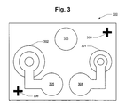
- FIG. 3 illustrates an exemplary multi-aperture VCSEL in accordance with one aspect of the subject disclosure, in which apertures of differing sizes are used to provide different levels of power from the same VCSEL.
- VCSEL 300 includes two similarly-shaped (e.g., circular) apertures 301 and 302 .
- the apertures 301 and 302 share the same multiple-layer mirror structure and bottom DBR mirror layer.
- Aperture 301 is smaller than aperture 302 , such that the power produced by aperture 301 is less than the power produced by aperture 302 .
- Apertures 301 and 302 share an n-bonding pad 303 but are connected to separate p-bonding pads 304 and 305 , respectively, such that each aperture is on a different circuit.
- This configuration may be used to separately switch apertures 301 and 302 to provide multiple levels of power (e.g., powering only aperture 301 for a lowest power level, powering only aperture 302 for a higher power level, and powering both aperture 301 and 302 for a highest power level). Different levels of power may be desirable based upon the operating temperature of the magnetic recording media to be written (e.g., when the temperature of the media is lower, more power may be used to locally heat a spot for writing than when the temperature of the media is higher).
- VCSEL 300 further includes alignment marks 306 , which may be used to help align VCSEL 300 with another device to which it may be attached by, e.g., wafer-level bonding.
- different apertures on a multiple aperture VCSEL may be located on different circuits (e.g., by connecting them to separate anodes, separate cathodes, or separate anodes and cathodes), in accordance with various aspects of the subject disclosure.
- Separately switching laser apertures on the same VCSEL allows for providing differing levels of power and for redundancy and/or yield (in the event one laser aperture is defective or malfunctions, additional laser apertures may be available).
- Configuring different apertures to share at least one bonding pad may simplify the fabrication of a VCSEL and its integration to passive light delivery waveguides.
- VCSELs with exactly two apertures each have been illustrated, the scope of the present invention is not limited to such an arrangement. Rather, VCSELs with any number of apertures greater than one may be utilized to provide varying levels of power to EAMR heads.
- FIG. 4 illustrates a magnetic recording device comprising a multiple-aperture VCSEL in accordance with one aspect of the subject disclosure.
- Magnetic recording device 400 includes a multiple-aperture VCSEL 401 attached to a magnetic recording head 402 .
- VCSEL 401 and magnetic recording head 402 include alignment marks 410 , which are used to help align VCSEL 401 with magnetic recording head 402 during the attachment of VCSEL 401 to magnetic recording head 402 .
- Apertures 403 and 404 of VCSEL 401 are coupled to waveguides 405 and 406 , such that the laser light produced thereby is coupled into the magnetic recording head 402 .
- the coupling of apertures 403 and 404 to waveguides 405 and 406 may be realized through any one of a number of methods known to those of skill in the art (e.g., grating assisted coupling or the like).
- Waveguides 405 and 406 direct the laser light to a near field transducer (NFT) 407 , which concentrates the energy thereof to a nano-sized spot on recording medium 408 .
- NFT 407 may be disposed in a layer of magnetic recording head 402 between write pole 409 and a return pole. By configuring NFT 407 to be in resonance with and shared by both waveguides 405 and 406 , the heating capability thereof may be doubled (when compared to an NFT illuminated by a single waveguide).
- aperture 403 and 404 may be configured to provide laser light of a preferred polarization (e.g., both apertures may be configured to provide a linearly polarized mode such that the light in the respective waveguide is in a TE or a TM mode).
- NFT 407 may be configured to couple with either a TM or a TE mode of light from the VCSEL.
- waveguides 405 and 406 are on opposite sides of write pole 409 , such that write pole 409 does not interfere with the propagation of light in waveguides 405 and 406 , and waveguides 405 and 406 do not adversely impact the write performance of write pole 409 .
- waveguides 405 and 406 may have the same path length, and may moreover taper towards NFT 407 .
- Waveguides 405 and 406 are curvilinear, such that the ends of waveguides 405 and 406 that couple with the edges of NFT 407 are on opposite sides of NFT. This configuration allows NFT 407 to be designed such that the edges which couple with the ends of waveguides 405 and 406 are perpendicular to a direction of propagation of light in the waveguides, improving the coupling efficiency of the connection.
- FIG. 5 illustrates a magnetic recording device comprising a multiple-aperture VCSEL in accordance with another aspect of the subject disclosure.
- Magnetic recording device 500 includes a multiple-aperture VCSEL 501 attached to a magnetic recording head 502 .
- VCSEL 501 and magnetic recording head 502 include alignment marks 511 , which are used to help align VCSEL 501 with magnetic recording head 502 during the attachment of VCSEL 501 to magnetic recording head 502 .
- Apertures 503 and 504 of VCSEL 501 are coupled to waveguides 505 and 506 , such that the laser light produced thereby is coupled into the magnetic recording head 502 .
- the coupling of apertures 503 and 504 to waveguides 505 and 506 may be realized through any one of a number of methods known to those of skill in the art (e.g., grating assisted coupling or the like).
- Waveguides 505 and 506 direct the laser light to another waveguide 507 , where the light is combined before being delivered to a near field transducer (NFT) 508 .
- NFT 508 concentrates the energy from waveguide 507 to a nano-sized spot on recording medium 509 . This heated region experiences a lower magnetic coercivity, such that magnetic write pole 510 is able to change the magnetic orientation thereof in a write operation.
- NFT 508 may be disposed in a layer of magnetic recording head 502 between write pole 510 and a return pole.
- waveguide 507 is located to one side of write pole 510 , such that write pole 510 does not interfere with the propagation of light in waveguide 507 , and waveguide 507 does not adversely impact the write performance of write pole 510 .
- the end of waveguide 507 couples with an edge of NFT 508 which is approximately perpendicular to the air bearing surface of magnetic recording head 502 .
- This configuration allows NFT 508 to be designed such that the edge which couples with the end of waveguide 507 is perpendicular to a direction of propagation of light in waveguide 507 , improving the coupling efficiency of the connection.
- FIG. 6 is a graph illustrating the simulation results of a symmetric waveguide combiner, such as is illustrated in FIG. 5 , in accordance with one aspect of the subject disclosure.
- properly designed waveguide combiners can couple in-phase light with nearly no loss (e.g., 50% power in each individual waveguide leg is coupled to provide nearly 100% power).
- the efficiency of the combiner will detract very little from the efficiency of the overall light delivery system.
- Various embodiments of the subject disclosure enjoy a number of benefits when compared with other EAMR systems and methods.
- the optical power of a single VCSEL die can be increased without a corresponding increase in the wafer or process cost.
- a common electrical pad layout can be maintained for easy integration with an EAMR controller.
- multiple waveguides are used to deliver light from the multiple aperture VCSEL to a NFT, interference with the performance of the magnetic write pole can be avoided. Biasing the shape and orientation of the apertures on the VCSEL allows for optimized optical coupling into the waveguides.
- FIG. 7 is a flow chart illustrating a method of using a magnetic recording device in accordance with one aspect of the subject disclosure.
- the method begins with step 701 , in which a plurality of waveguides disposed in a magnetic recording head are illuminated with a corresponding plurality of apertures of a multi-aperture VCSEL. Each of the plurality of waveguides has a second end coupled to a near field transducer of the magnetic recording head, whereby the near field transducer heats a region of magnetic recording media adjacent thereto.
- step 702 in which a write pole of the magnetic recording head generates a magnetic field in the region of magnetic recording media to change a magnetic orientation thereof.
Abstract
Description
Claims (21)
Priority Applications (1)
| Application Number | Priority Date | Filing Date | Title |
|---|---|---|---|
| US12/468,813 US8077557B1 (en) | 2009-05-19 | 2009-05-19 | Multiple aperture VCSEL EAMR heads |
Applications Claiming Priority (1)
| Application Number | Priority Date | Filing Date | Title |
|---|---|---|---|
| US12/468,813 US8077557B1 (en) | 2009-05-19 | 2009-05-19 | Multiple aperture VCSEL EAMR heads |
Publications (1)
| Publication Number | Publication Date |
|---|---|
| US8077557B1 true US8077557B1 (en) | 2011-12-13 |
Family
ID=45092714
Family Applications (1)
| Application Number | Title | Priority Date | Filing Date |
|---|---|---|---|
| US12/468,813 Active 2030-03-03 US8077557B1 (en) | 2009-05-19 | 2009-05-19 | Multiple aperture VCSEL EAMR heads |
Country Status (1)
| Country | Link |
|---|---|
| US (1) | US8077557B1 (en) |
Cited By (135)
| Publication number | Priority date | Publication date | Assignee | Title |
|---|---|---|---|---|
| US8670294B1 (en) * | 2012-02-17 | 2014-03-11 | Western Digital (Fremont), Llc | Systems and methods for increasing media absorption efficiency using interferometric waveguides |
| US8675455B1 (en) * | 2012-02-17 | 2014-03-18 | Western Digital (Fremont), Llc | Systems and methods for controlling light phase difference in interferometric waveguides at near field transducers |
| US8830628B1 (en) | 2009-02-23 | 2014-09-09 | Western Digital (Fremont), Llc | Method and system for providing a perpendicular magnetic recording head |
| US8879207B1 (en) | 2011-12-20 | 2014-11-04 | Western Digital (Fremont), Llc | Method for providing a side shield for a magnetic recording transducer using an air bridge |
| US8883017B1 (en) | 2013-03-12 | 2014-11-11 | Western Digital (Fremont), Llc | Method and system for providing a read transducer having seamless interfaces |
| US8917581B1 (en) | 2013-12-18 | 2014-12-23 | Western Digital Technologies, Inc. | Self-anneal process for a near field transducer and chimney in a hard disk drive assembly |
| US8923102B1 (en) | 2013-07-16 | 2014-12-30 | Western Digital (Fremont), Llc | Optical grating coupling for interferometric waveguides in heat assisted magnetic recording heads |
| US8947985B1 (en) | 2013-07-16 | 2015-02-03 | Western Digital (Fremont), Llc | Heat assisted magnetic recording transducers having a recessed pole |
| US8953422B1 (en) * | 2014-06-10 | 2015-02-10 | Western Digital (Fremont), Llc | Near field transducer using dielectric waveguide core with fine ridge feature |
| US8958272B1 (en) * | 2014-06-10 | 2015-02-17 | Western Digital (Fremont), Llc | Interfering near field transducer for energy assisted magnetic recording |
| US8970988B1 (en) | 2013-12-31 | 2015-03-03 | Western Digital (Fremont), Llc | Electric gaps and method for making electric gaps for multiple sensor arrays |
| US8971160B1 (en) | 2013-12-19 | 2015-03-03 | Western Digital (Fremont), Llc | Near field transducer with high refractive index pin for heat assisted magnetic recording |
| US8976635B1 (en) | 2014-06-10 | 2015-03-10 | Western Digital (Fremont), Llc | Near field transducer driven by a transverse electric waveguide for energy assisted magnetic recording |
| US8980109B1 (en) | 2012-12-11 | 2015-03-17 | Western Digital (Fremont), Llc | Method for providing a magnetic recording transducer using a combined main pole and side shield CMP for a wraparound shield scheme |
| US8982508B1 (en) | 2011-10-31 | 2015-03-17 | Western Digital (Fremont), Llc | Method for providing a side shield for a magnetic recording transducer |
| US8988812B1 (en) | 2013-11-27 | 2015-03-24 | Western Digital (Fremont), Llc | Multi-sensor array configuration for a two-dimensional magnetic recording (TDMR) operation |
| US8984740B1 (en) | 2012-11-30 | 2015-03-24 | Western Digital (Fremont), Llc | Process for providing a magnetic recording transducer having a smooth magnetic seed layer |
| US8988825B1 (en) | 2014-02-28 | 2015-03-24 | Western Digital (Fremont, LLC | Method for fabricating a magnetic writer having half-side shields |
| US8995087B1 (en) | 2006-11-29 | 2015-03-31 | Western Digital (Fremont), Llc | Perpendicular magnetic recording write head having a wrap around shield |
| US8993217B1 (en) | 2013-04-04 | 2015-03-31 | Western Digital (Fremont), Llc | Double exposure technique for high resolution disk imaging |
| US9001628B1 (en) | 2013-12-16 | 2015-04-07 | Western Digital (Fremont), Llc | Assistant waveguides for evaluating main waveguide coupling efficiency and diode laser alignment tolerances for hard disk |
| US8997832B1 (en) | 2010-11-23 | 2015-04-07 | Western Digital (Fremont), Llc | Method of fabricating micrometer scale components |
| US9001467B1 (en) | 2014-03-05 | 2015-04-07 | Western Digital (Fremont), Llc | Method for fabricating side shields in a magnetic writer |
| US9007879B1 (en) | 2014-06-10 | 2015-04-14 | Western Digital (Fremont), Llc | Interfering near field transducer having a wide metal bar feature for energy assisted magnetic recording |
| US9007719B1 (en) | 2013-10-23 | 2015-04-14 | Western Digital (Fremont), Llc | Systems and methods for using double mask techniques to achieve very small features |
| US9007725B1 (en) | 2014-10-07 | 2015-04-14 | Western Digital (Fremont), Llc | Sensor with positive coupling between dual ferromagnetic free layer laminates |
| US9013836B1 (en) | 2013-04-02 | 2015-04-21 | Western Digital (Fremont), Llc | Method and system for providing an antiferromagnetically coupled return pole |
| US9042052B1 (en) | 2014-06-23 | 2015-05-26 | Western Digital (Fremont), Llc | Magnetic writer having a partially shunted coil |
| US9042058B1 (en) | 2013-10-17 | 2015-05-26 | Western Digital Technologies, Inc. | Shield designed for middle shields in a multiple sensor array |
| US9042057B1 (en) | 2013-01-09 | 2015-05-26 | Western Digital (Fremont), Llc | Methods for providing magnetic storage elements with high magneto-resistance using Heusler alloys |
| US9042051B2 (en) | 2013-08-15 | 2015-05-26 | Western Digital (Fremont), Llc | Gradient write gap for perpendicular magnetic recording writer |
| US9042208B1 (en) | 2013-03-11 | 2015-05-26 | Western Digital Technologies, Inc. | Disk drive measuring fly height by applying a bias voltage to an electrically insulated write component of a head |
| US9053735B1 (en) | 2014-06-20 | 2015-06-09 | Western Digital (Fremont), Llc | Method for fabricating a magnetic writer using a full-film metal planarization |
| US9064527B1 (en) | 2013-04-12 | 2015-06-23 | Western Digital (Fremont), Llc | High order tapered waveguide for use in a heat assisted magnetic recording head |
| US9065043B1 (en) | 2012-06-29 | 2015-06-23 | Western Digital (Fremont), Llc | Tunnel magnetoresistance read head with narrow shield-to-shield spacing |
| US9064528B1 (en) | 2013-05-17 | 2015-06-23 | Western Digital Technologies, Inc. | Interferometric waveguide usable in shingled heat assisted magnetic recording in the absence of a near-field transducer |
| US9064507B1 (en) | 2009-07-31 | 2015-06-23 | Western Digital (Fremont), Llc | Magnetic etch-stop layer for magnetoresistive read heads |
| US9070381B1 (en) | 2013-04-12 | 2015-06-30 | Western Digital (Fremont), Llc | Magnetic recording read transducer having a laminated free layer |
| US9082423B1 (en) | 2013-12-18 | 2015-07-14 | Western Digital (Fremont), Llc | Magnetic recording write transducer having an improved trailing surface profile |
| US9087527B1 (en) | 2014-10-28 | 2015-07-21 | Western Digital (Fremont), Llc | Apparatus and method for middle shield connection in magnetic recording transducers |
| US9087534B1 (en) | 2011-12-20 | 2015-07-21 | Western Digital (Fremont), Llc | Method and system for providing a read transducer having soft and hard magnetic bias structures |
| US9093639B2 (en) | 2012-02-21 | 2015-07-28 | Western Digital (Fremont), Llc | Methods for manufacturing a magnetoresistive structure utilizing heating and cooling |
| US9104107B1 (en) | 2013-04-03 | 2015-08-11 | Western Digital (Fremont), Llc | DUV photoresist process |
| US9111550B1 (en) | 2014-12-04 | 2015-08-18 | Western Digital (Fremont), Llc | Write transducer having a magnetic buffer layer spaced between a side shield and a write pole by non-magnetic layers |
| US9111558B1 (en) | 2014-03-14 | 2015-08-18 | Western Digital (Fremont), Llc | System and method of diffractive focusing of light in a waveguide |
| US9111564B1 (en) | 2013-04-02 | 2015-08-18 | Western Digital (Fremont), Llc | Magnetic recording writer having a main pole with multiple flare angles |
| US9123359B1 (en) | 2010-12-22 | 2015-09-01 | Western Digital (Fremont), Llc | Magnetic recording transducer with sputtered antiferromagnetic coupling trilayer between plated ferromagnetic shields and method of fabrication |
| US9123358B1 (en) | 2012-06-11 | 2015-09-01 | Western Digital (Fremont), Llc | Conformal high moment side shield seed layer for perpendicular magnetic recording writer |
| US9123374B1 (en) | 2015-02-12 | 2015-09-01 | Western Digital (Fremont), Llc | Heat assisted magnetic recording writer having an integrated polarization rotation plate |
| US9123362B1 (en) | 2011-03-22 | 2015-09-01 | Western Digital (Fremont), Llc | Methods for assembling an electrically assisted magnetic recording (EAMR) head |
| US9135937B1 (en) | 2014-05-09 | 2015-09-15 | Western Digital (Fremont), Llc | Current modulation on laser diode for energy assisted magnetic recording transducer |
| US9135930B1 (en) | 2014-03-06 | 2015-09-15 | Western Digital (Fremont), Llc | Method for fabricating a magnetic write pole using vacuum deposition |
| US9142233B1 (en) | 2014-02-28 | 2015-09-22 | Western Digital (Fremont), Llc | Heat assisted magnetic recording writer having a recessed pole |
| US9147404B1 (en) | 2015-03-31 | 2015-09-29 | Western Digital (Fremont), Llc | Method and system for providing a read transducer having a dual free layer |
| US9147408B1 (en) | 2013-12-19 | 2015-09-29 | Western Digital (Fremont), Llc | Heated AFM layer deposition and cooling process for TMR magnetic recording sensor with high pinning field |
| US9153255B1 (en) | 2014-03-05 | 2015-10-06 | Western Digital (Fremont), Llc | Method for fabricating a magnetic writer having an asymmetric gap and shields |
| US9183854B2 (en) | 2014-02-24 | 2015-11-10 | Western Digital (Fremont), Llc | Method to make interferometric taper waveguide for HAMR light delivery |
| US9190085B1 (en) | 2014-03-12 | 2015-11-17 | Western Digital (Fremont), Llc | Waveguide with reflective grating for localized energy intensity |
| US9190079B1 (en) | 2014-09-22 | 2015-11-17 | Western Digital (Fremont), Llc | Magnetic write pole having engineered radius of curvature and chisel angle profiles |
| US9194692B1 (en) | 2013-12-06 | 2015-11-24 | Western Digital (Fremont), Llc | Systems and methods for using white light interferometry to measure undercut of a bi-layer structure |
| US9202493B1 (en) | 2014-02-28 | 2015-12-01 | Western Digital (Fremont), Llc | Method of making an ultra-sharp tip mode converter for a HAMR head |
| US9202480B2 (en) | 2009-10-14 | 2015-12-01 | Western Digital (Fremont), LLC. | Double patterning hard mask for damascene perpendicular magnetic recording (PMR) writer |
| US9214169B1 (en) | 2014-06-20 | 2015-12-15 | Western Digital (Fremont), Llc | Magnetic recording read transducer having a laminated free layer |
| US9214165B1 (en) | 2014-12-18 | 2015-12-15 | Western Digital (Fremont), Llc | Magnetic writer having a gradient in saturation magnetization of the shields |
| US9213322B1 (en) | 2012-08-16 | 2015-12-15 | Western Digital (Fremont), Llc | Methods for providing run to run process control using a dynamic tuner |
| US9214172B2 (en) | 2013-10-23 | 2015-12-15 | Western Digital (Fremont), Llc | Method of manufacturing a magnetic read head |
| US9230565B1 (en) | 2014-06-24 | 2016-01-05 | Western Digital (Fremont), Llc | Magnetic shield for magnetic recording head |
| US9236560B1 (en) | 2014-12-08 | 2016-01-12 | Western Digital (Fremont), Llc | Spin transfer torque tunneling magnetoresistive device having a laminated free layer with perpendicular magnetic anisotropy |
| US9245562B1 (en) | 2015-03-30 | 2016-01-26 | Western Digital (Fremont), Llc | Magnetic recording writer with a composite main pole |
| US9245545B1 (en) | 2013-04-12 | 2016-01-26 | Wester Digital (Fremont), Llc | Short yoke length coils for magnetic heads in disk drives |
| US9245543B1 (en) | 2010-06-25 | 2016-01-26 | Western Digital (Fremont), Llc | Method for providing an energy assisted magnetic recording head having a laser integrally mounted to the slider |
| US9251813B1 (en) | 2009-04-19 | 2016-02-02 | Western Digital (Fremont), Llc | Method of making a magnetic recording head |
| US9263067B1 (en) | 2013-05-29 | 2016-02-16 | Western Digital (Fremont), Llc | Process for making PMR writer with constant side wall angle |
| US9263071B1 (en) | 2015-03-31 | 2016-02-16 | Western Digital (Fremont), Llc | Flat NFT for heat assisted magnetic recording |
| US9269382B1 (en) | 2012-06-29 | 2016-02-23 | Western Digital (Fremont), Llc | Method and system for providing a read transducer having improved pinning of the pinned layer at higher recording densities |
| US9275657B1 (en) | 2013-08-14 | 2016-03-01 | Western Digital (Fremont), Llc | Process for making PMR writer with non-conformal side gaps |
| US9280990B1 (en) | 2013-12-11 | 2016-03-08 | Western Digital (Fremont), Llc | Method for fabricating a magnetic writer using multiple etches |
| US9287494B1 (en) | 2013-06-28 | 2016-03-15 | Western Digital (Fremont), Llc | Magnetic tunnel junction (MTJ) with a magnesium oxide tunnel barrier |
| US9286919B1 (en) | 2014-12-17 | 2016-03-15 | Western Digital (Fremont), Llc | Magnetic writer having a dual side gap |
| US9286920B1 (en) | 2013-01-31 | 2016-03-15 | Western Digital (Fremont), Llc | Method for compensating for phase variations in an interferometric tapered waveguide in a heat assisted magnetic recording head |
| US9305583B1 (en) | 2014-02-18 | 2016-04-05 | Western Digital (Fremont), Llc | Method for fabricating a magnetic writer using multiple etches of damascene materials |
| US9312064B1 (en) | 2015-03-02 | 2016-04-12 | Western Digital (Fremont), Llc | Method to fabricate a magnetic head including ion milling of read gap using dual layer hard mask |
| US9318130B1 (en) | 2013-07-02 | 2016-04-19 | Western Digital (Fremont), Llc | Method to fabricate tunneling magnetic recording heads with extended pinned layer |
| US9336814B1 (en) | 2013-03-12 | 2016-05-10 | Western Digital (Fremont), Llc | Inverse tapered waveguide for use in a heat assisted magnetic recording head |
| US9343086B1 (en) | 2013-09-11 | 2016-05-17 | Western Digital (Fremont), Llc | Magnetic recording write transducer having an improved sidewall angle profile |
| US9343098B1 (en) | 2013-08-23 | 2016-05-17 | Western Digital (Fremont), Llc | Method for providing a heat assisted magnetic recording transducer having protective pads |
| US9343087B1 (en) | 2014-12-21 | 2016-05-17 | Western Digital (Fremont), Llc | Method for fabricating a magnetic writer having half shields |
| US9349392B1 (en) | 2012-05-24 | 2016-05-24 | Western Digital (Fremont), Llc | Methods for improving adhesion on dielectric substrates |
| US9349394B1 (en) | 2013-10-18 | 2016-05-24 | Western Digital (Fremont), Llc | Method for fabricating a magnetic writer having a gradient side gap |
| US9361914B1 (en) | 2014-06-18 | 2016-06-07 | Western Digital (Fremont), Llc | Magnetic sensor with thin capping layer |
| US9361913B1 (en) | 2013-06-03 | 2016-06-07 | Western Digital (Fremont), Llc | Recording read heads with a multi-layer AFM layer methods and apparatuses |
| US9368134B1 (en) | 2010-12-16 | 2016-06-14 | Western Digital (Fremont), Llc | Method and system for providing an antiferromagnetically coupled writer |
| US9384763B1 (en) | 2015-03-26 | 2016-07-05 | Western Digital (Fremont), Llc | Dual free layer magnetic reader having a rear bias structure including a soft bias layer |
| US9384765B1 (en) | 2015-09-24 | 2016-07-05 | Western Digital (Fremont), Llc | Method and system for providing a HAMR writer having improved optical efficiency |
| US9396743B1 (en) | 2014-02-28 | 2016-07-19 | Western Digital (Fremont), Llc | Systems and methods for controlling soft bias thickness for tunnel magnetoresistance readers |
| US9396742B1 (en) | 2012-11-30 | 2016-07-19 | Western Digital (Fremont), Llc | Magnetoresistive sensor for a magnetic storage system read head, and fabrication method thereof |
| US9406331B1 (en) | 2013-06-17 | 2016-08-02 | Western Digital (Fremont), Llc | Method for making ultra-narrow read sensor and read transducer device resulting therefrom |
| US9424866B1 (en) | 2015-09-24 | 2016-08-23 | Western Digital (Fremont), Llc | Heat assisted magnetic recording write apparatus having a dielectric gap |
| US9431047B1 (en) | 2013-05-01 | 2016-08-30 | Western Digital (Fremont), Llc | Method for providing an improved AFM reader shield |
| US9431039B1 (en) | 2013-05-21 | 2016-08-30 | Western Digital (Fremont), Llc | Multiple sensor array usable in two-dimensional magnetic recording |
| US9431038B1 (en) | 2015-06-29 | 2016-08-30 | Western Digital (Fremont), Llc | Method for fabricating a magnetic write pole having an improved sidewall angle profile |
| US9431032B1 (en) | 2013-08-14 | 2016-08-30 | Western Digital (Fremont), Llc | Electrical connection arrangement for a multiple sensor array usable in two-dimensional magnetic recording |
| US9431031B1 (en) | 2015-03-24 | 2016-08-30 | Western Digital (Fremont), Llc | System and method for magnetic transducers having multiple sensors and AFC shields |
| US9437251B1 (en) | 2014-12-22 | 2016-09-06 | Western Digital (Fremont), Llc | Apparatus and method having TDMR reader to reader shunts |
| US9441938B1 (en) | 2013-10-08 | 2016-09-13 | Western Digital (Fremont), Llc | Test structures for measuring near field transducer disc length |
| US9443541B1 (en) | 2015-03-24 | 2016-09-13 | Western Digital (Fremont), Llc | Magnetic writer having a gradient in saturation magnetization of the shields and return pole |
| US9449621B1 (en) | 2015-03-26 | 2016-09-20 | Western Digital (Fremont), Llc | Dual free layer magnetic reader having a rear bias structure having a high aspect ratio |
| US9449625B1 (en) | 2014-12-24 | 2016-09-20 | Western Digital (Fremont), Llc | Heat assisted magnetic recording head having a plurality of diffusion barrier layers |
| US9472216B1 (en) | 2015-09-23 | 2016-10-18 | Western Digital (Fremont), Llc | Differential dual free layer magnetic reader |
| US9484051B1 (en) | 2015-11-09 | 2016-11-01 | The Provost, Fellows, Foundation Scholars and the other members of Board, of the College of the Holy and Undivided Trinity of Queen Elizabeth near Dublin | Method and system for reducing undesirable reflections in a HAMR write apparatus |
| US9508372B1 (en) | 2015-06-03 | 2016-11-29 | Western Digital (Fremont), Llc | Shingle magnetic writer having a low sidewall angle pole |
| US9508365B1 (en) | 2015-06-24 | 2016-11-29 | Western Digital (Fremont), LLC. | Magnetic reader having a crystal decoupling structure |
| US9508363B1 (en) | 2014-06-17 | 2016-11-29 | Western Digital (Fremont), Llc | Method for fabricating a magnetic write pole having a leading edge bevel |
| US9530443B1 (en) | 2015-06-25 | 2016-12-27 | Western Digital (Fremont), Llc | Method for fabricating a magnetic recording device having a high aspect ratio structure |
| US9564150B1 (en) | 2015-11-24 | 2017-02-07 | Western Digital (Fremont), Llc | Magnetic read apparatus having an improved read sensor isolation circuit |
| US9595273B1 (en) | 2015-09-30 | 2017-03-14 | Western Digital (Fremont), Llc | Shingle magnetic writer having nonconformal shields |
| US9646639B2 (en) | 2015-06-26 | 2017-05-09 | Western Digital (Fremont), Llc | Heat assisted magnetic recording writer having integrated polarization rotation waveguides |
| US9666214B1 (en) | 2015-09-23 | 2017-05-30 | Western Digital (Fremont), Llc | Free layer magnetic reader that may have a reduced shield-to-shield spacing |
| US9721595B1 (en) | 2014-12-04 | 2017-08-01 | Western Digital (Fremont), Llc | Method for providing a storage device |
| US9740805B1 (en) | 2015-12-01 | 2017-08-22 | Western Digital (Fremont), Llc | Method and system for detecting hotspots for photolithographically-defined devices |
| US9741366B1 (en) | 2014-12-18 | 2017-08-22 | Western Digital (Fremont), Llc | Method for fabricating a magnetic writer having a gradient in saturation magnetization of the shields |
| US9754611B1 (en) | 2015-11-30 | 2017-09-05 | Western Digital (Fremont), Llc | Magnetic recording write apparatus having a stepped conformal trailing shield |
| US9767831B1 (en) | 2015-12-01 | 2017-09-19 | Western Digital (Fremont), Llc | Magnetic writer having convex trailing surface pole and conformal write gap |
| US9786301B1 (en) | 2014-12-02 | 2017-10-10 | Western Digital (Fremont), Llc | Apparatuses and methods for providing thin shields in a multiple sensor array |
| US9799351B1 (en) | 2015-11-30 | 2017-10-24 | Western Digital (Fremont), Llc | Short yoke length writer having assist coils |
| US9812155B1 (en) | 2015-11-23 | 2017-11-07 | Western Digital (Fremont), Llc | Method and system for fabricating high junction angle read sensors |
| US9842615B1 (en) | 2015-06-26 | 2017-12-12 | Western Digital (Fremont), Llc | Magnetic reader having a nonmagnetic insertion layer for the pinning layer |
| US9858951B1 (en) | 2015-12-01 | 2018-01-02 | Western Digital (Fremont), Llc | Method for providing a multilayer AFM layer in a read sensor |
| US9881638B1 (en) | 2014-12-17 | 2018-01-30 | Western Digital (Fremont), Llc | Method for providing a near-field transducer (NFT) for a heat assisted magnetic recording (HAMR) device |
| US9934811B1 (en) | 2014-03-07 | 2018-04-03 | Western Digital (Fremont), Llc | Methods for controlling stray fields of magnetic features using magneto-elastic anisotropy |
| US9953670B1 (en) | 2015-11-10 | 2018-04-24 | Western Digital (Fremont), Llc | Method and system for providing a HAMR writer including a multi-mode interference device |
| US10037770B1 (en) | 2015-11-12 | 2018-07-31 | Western Digital (Fremont), Llc | Method for providing a magnetic recording write apparatus having a seamless pole |
| US10074387B1 (en) | 2014-12-21 | 2018-09-11 | Western Digital (Fremont), Llc | Method and system for providing a read transducer having symmetric antiferromagnetically coupled shields |
| US11302352B2 (en) | 2020-06-22 | 2022-04-12 | Western Digital Technologies, Inc. | VCSEL array for HAMR |
| US11657845B1 (en) | 2022-03-30 | 2023-05-23 | Western Digital Technologies, Inc. | Beam combiner for VCSEL array in HAMR head |
Citations (11)
| Publication number | Priority date | Publication date | Assignee | Title |
|---|---|---|---|---|
| US5831960A (en) | 1997-07-17 | 1998-11-03 | Motorola, Inc. | Integrated vertical cavity surface emitting laser pair for high density data storage and method of fabrication |
| US6023450A (en) | 1996-10-29 | 2000-02-08 | Samsung Electronics Co., Ltd. | Multiple beam optical pickup using a vertical cavity surface emitting laser array |
| US6795630B2 (en) * | 2002-06-28 | 2004-09-21 | Seagate Technology Llc | Apparatus and method for producing a small spot of optical energy |
| US6807131B1 (en) | 2000-12-27 | 2004-10-19 | Research Investment Network, Inc. | Near-field hybrid magnetic-optical head system |
| US6834027B1 (en) | 2000-02-28 | 2004-12-21 | Nec Laboratories America, Inc. | Surface plasmon-enhanced read/write heads for optical data storage media |
| US7069569B2 (en) | 2000-02-01 | 2006-06-27 | Research Investment Network, Inc. | Near-field optical head system with integrated slider and laser |
| US7158470B2 (en) | 2000-02-01 | 2007-01-02 | Research Investment Network, Inc. | Near-field optical head system with integrated slider and laser |
| WO2007133036A1 (en) | 2006-05-17 | 2007-11-22 | Samsung Electronics Co., Ltd. | Heat-assisted magnetic recording head gimbal assembly |
| US7310206B2 (en) | 2004-12-28 | 2007-12-18 | Sae Magnetics (H.K.) Ltd. | Magnetic thin film head with heat-assisted write section and hard disk drive incorporating same |
| US20080056073A1 (en) * | 2006-08-30 | 2008-03-06 | Junichiro Shimizu | Recording head |
| US20080316872A1 (en) * | 2007-06-21 | 2008-12-25 | Junichiro Shimizu | Optical device integrated head |
-
2009
- 2009-05-19 US US12/468,813 patent/US8077557B1/en active Active
Patent Citations (11)
| Publication number | Priority date | Publication date | Assignee | Title |
|---|---|---|---|---|
| US6023450A (en) | 1996-10-29 | 2000-02-08 | Samsung Electronics Co., Ltd. | Multiple beam optical pickup using a vertical cavity surface emitting laser array |
| US5831960A (en) | 1997-07-17 | 1998-11-03 | Motorola, Inc. | Integrated vertical cavity surface emitting laser pair for high density data storage and method of fabrication |
| US7069569B2 (en) | 2000-02-01 | 2006-06-27 | Research Investment Network, Inc. | Near-field optical head system with integrated slider and laser |
| US7158470B2 (en) | 2000-02-01 | 2007-01-02 | Research Investment Network, Inc. | Near-field optical head system with integrated slider and laser |
| US6834027B1 (en) | 2000-02-28 | 2004-12-21 | Nec Laboratories America, Inc. | Surface plasmon-enhanced read/write heads for optical data storage media |
| US6807131B1 (en) | 2000-12-27 | 2004-10-19 | Research Investment Network, Inc. | Near-field hybrid magnetic-optical head system |
| US6795630B2 (en) * | 2002-06-28 | 2004-09-21 | Seagate Technology Llc | Apparatus and method for producing a small spot of optical energy |
| US7310206B2 (en) | 2004-12-28 | 2007-12-18 | Sae Magnetics (H.K.) Ltd. | Magnetic thin film head with heat-assisted write section and hard disk drive incorporating same |
| WO2007133036A1 (en) | 2006-05-17 | 2007-11-22 | Samsung Electronics Co., Ltd. | Heat-assisted magnetic recording head gimbal assembly |
| US20080056073A1 (en) * | 2006-08-30 | 2008-03-06 | Junichiro Shimizu | Recording head |
| US20080316872A1 (en) * | 2007-06-21 | 2008-12-25 | Junichiro Shimizu | Optical device integrated head |
Cited By (157)
| Publication number | Priority date | Publication date | Assignee | Title |
|---|---|---|---|---|
| US8995087B1 (en) | 2006-11-29 | 2015-03-31 | Western Digital (Fremont), Llc | Perpendicular magnetic recording write head having a wrap around shield |
| US8830628B1 (en) | 2009-02-23 | 2014-09-09 | Western Digital (Fremont), Llc | Method and system for providing a perpendicular magnetic recording head |
| US9251813B1 (en) | 2009-04-19 | 2016-02-02 | Western Digital (Fremont), Llc | Method of making a magnetic recording head |
| US9064507B1 (en) | 2009-07-31 | 2015-06-23 | Western Digital (Fremont), Llc | Magnetic etch-stop layer for magnetoresistive read heads |
| US9202480B2 (en) | 2009-10-14 | 2015-12-01 | Western Digital (Fremont), LLC. | Double patterning hard mask for damascene perpendicular magnetic recording (PMR) writer |
| US9245543B1 (en) | 2010-06-25 | 2016-01-26 | Western Digital (Fremont), Llc | Method for providing an energy assisted magnetic recording head having a laser integrally mounted to the slider |
| US9672847B2 (en) | 2010-11-23 | 2017-06-06 | Western Digital (Fremont), Llc | Micrometer scale components |
| US9159345B1 (en) | 2010-11-23 | 2015-10-13 | Western Digital (Fremont), Llc | Micrometer scale components |
| US8997832B1 (en) | 2010-11-23 | 2015-04-07 | Western Digital (Fremont), Llc | Method of fabricating micrometer scale components |
| US9368134B1 (en) | 2010-12-16 | 2016-06-14 | Western Digital (Fremont), Llc | Method and system for providing an antiferromagnetically coupled writer |
| US9123359B1 (en) | 2010-12-22 | 2015-09-01 | Western Digital (Fremont), Llc | Magnetic recording transducer with sputtered antiferromagnetic coupling trilayer between plated ferromagnetic shields and method of fabrication |
| US9123362B1 (en) | 2011-03-22 | 2015-09-01 | Western Digital (Fremont), Llc | Methods for assembling an electrically assisted magnetic recording (EAMR) head |
| US8982508B1 (en) | 2011-10-31 | 2015-03-17 | Western Digital (Fremont), Llc | Method for providing a side shield for a magnetic recording transducer |
| US8879207B1 (en) | 2011-12-20 | 2014-11-04 | Western Digital (Fremont), Llc | Method for providing a side shield for a magnetic recording transducer using an air bridge |
| US9087534B1 (en) | 2011-12-20 | 2015-07-21 | Western Digital (Fremont), Llc | Method and system for providing a read transducer having soft and hard magnetic bias structures |
| US8675455B1 (en) * | 2012-02-17 | 2014-03-18 | Western Digital (Fremont), Llc | Systems and methods for controlling light phase difference in interferometric waveguides at near field transducers |
| US8670294B1 (en) * | 2012-02-17 | 2014-03-11 | Western Digital (Fremont), Llc | Systems and methods for increasing media absorption efficiency using interferometric waveguides |
| US9093639B2 (en) | 2012-02-21 | 2015-07-28 | Western Digital (Fremont), Llc | Methods for manufacturing a magnetoresistive structure utilizing heating and cooling |
| US9940950B2 (en) | 2012-05-24 | 2018-04-10 | Western Digital (Fremont), Llc | Methods for improving adhesion on dielectric substrates |
| US9349392B1 (en) | 2012-05-24 | 2016-05-24 | Western Digital (Fremont), Llc | Methods for improving adhesion on dielectric substrates |
| US9123358B1 (en) | 2012-06-11 | 2015-09-01 | Western Digital (Fremont), Llc | Conformal high moment side shield seed layer for perpendicular magnetic recording writer |
| US9269382B1 (en) | 2012-06-29 | 2016-02-23 | Western Digital (Fremont), Llc | Method and system for providing a read transducer having improved pinning of the pinned layer at higher recording densities |
| US9412400B2 (en) | 2012-06-29 | 2016-08-09 | Western Digital (Fremont), Llc | Tunnel magnetoresistance read head with narrow shield-to-shield spacing |
| US9065043B1 (en) | 2012-06-29 | 2015-06-23 | Western Digital (Fremont), Llc | Tunnel magnetoresistance read head with narrow shield-to-shield spacing |
| US9213322B1 (en) | 2012-08-16 | 2015-12-15 | Western Digital (Fremont), Llc | Methods for providing run to run process control using a dynamic tuner |
| US9396742B1 (en) | 2012-11-30 | 2016-07-19 | Western Digital (Fremont), Llc | Magnetoresistive sensor for a magnetic storage system read head, and fabrication method thereof |
| US8984740B1 (en) | 2012-11-30 | 2015-03-24 | Western Digital (Fremont), Llc | Process for providing a magnetic recording transducer having a smooth magnetic seed layer |
| US8980109B1 (en) | 2012-12-11 | 2015-03-17 | Western Digital (Fremont), Llc | Method for providing a magnetic recording transducer using a combined main pole and side shield CMP for a wraparound shield scheme |
| US9042057B1 (en) | 2013-01-09 | 2015-05-26 | Western Digital (Fremont), Llc | Methods for providing magnetic storage elements with high magneto-resistance using Heusler alloys |
| US9286920B1 (en) | 2013-01-31 | 2016-03-15 | Western Digital (Fremont), Llc | Method for compensating for phase variations in an interferometric tapered waveguide in a heat assisted magnetic recording head |
| US9042208B1 (en) | 2013-03-11 | 2015-05-26 | Western Digital Technologies, Inc. | Disk drive measuring fly height by applying a bias voltage to an electrically insulated write component of a head |
| US8883017B1 (en) | 2013-03-12 | 2014-11-11 | Western Digital (Fremont), Llc | Method and system for providing a read transducer having seamless interfaces |
| US9336814B1 (en) | 2013-03-12 | 2016-05-10 | Western Digital (Fremont), Llc | Inverse tapered waveguide for use in a heat assisted magnetic recording head |
| US9013836B1 (en) | 2013-04-02 | 2015-04-21 | Western Digital (Fremont), Llc | Method and system for providing an antiferromagnetically coupled return pole |
| US9111564B1 (en) | 2013-04-02 | 2015-08-18 | Western Digital (Fremont), Llc | Magnetic recording writer having a main pole with multiple flare angles |
| US9104107B1 (en) | 2013-04-03 | 2015-08-11 | Western Digital (Fremont), Llc | DUV photoresist process |
| US8993217B1 (en) | 2013-04-04 | 2015-03-31 | Western Digital (Fremont), Llc | Double exposure technique for high resolution disk imaging |
| US9064527B1 (en) | 2013-04-12 | 2015-06-23 | Western Digital (Fremont), Llc | High order tapered waveguide for use in a heat assisted magnetic recording head |
| US9245545B1 (en) | 2013-04-12 | 2016-01-26 | Wester Digital (Fremont), Llc | Short yoke length coils for magnetic heads in disk drives |
| US9070381B1 (en) | 2013-04-12 | 2015-06-30 | Western Digital (Fremont), Llc | Magnetic recording read transducer having a laminated free layer |
| US9431047B1 (en) | 2013-05-01 | 2016-08-30 | Western Digital (Fremont), Llc | Method for providing an improved AFM reader shield |
| US9064528B1 (en) | 2013-05-17 | 2015-06-23 | Western Digital Technologies, Inc. | Interferometric waveguide usable in shingled heat assisted magnetic recording in the absence of a near-field transducer |
| US9431039B1 (en) | 2013-05-21 | 2016-08-30 | Western Digital (Fremont), Llc | Multiple sensor array usable in two-dimensional magnetic recording |
| US9263067B1 (en) | 2013-05-29 | 2016-02-16 | Western Digital (Fremont), Llc | Process for making PMR writer with constant side wall angle |
| US9361913B1 (en) | 2013-06-03 | 2016-06-07 | Western Digital (Fremont), Llc | Recording read heads with a multi-layer AFM layer methods and apparatuses |
| US9406331B1 (en) | 2013-06-17 | 2016-08-02 | Western Digital (Fremont), Llc | Method for making ultra-narrow read sensor and read transducer device resulting therefrom |
| US9287494B1 (en) | 2013-06-28 | 2016-03-15 | Western Digital (Fremont), Llc | Magnetic tunnel junction (MTJ) with a magnesium oxide tunnel barrier |
| US9318130B1 (en) | 2013-07-02 | 2016-04-19 | Western Digital (Fremont), Llc | Method to fabricate tunneling magnetic recording heads with extended pinned layer |
| US8947985B1 (en) | 2013-07-16 | 2015-02-03 | Western Digital (Fremont), Llc | Heat assisted magnetic recording transducers having a recessed pole |
| US8923102B1 (en) | 2013-07-16 | 2014-12-30 | Western Digital (Fremont), Llc | Optical grating coupling for interferometric waveguides in heat assisted magnetic recording heads |
| US9431032B1 (en) | 2013-08-14 | 2016-08-30 | Western Digital (Fremont), Llc | Electrical connection arrangement for a multiple sensor array usable in two-dimensional magnetic recording |
| US9275657B1 (en) | 2013-08-14 | 2016-03-01 | Western Digital (Fremont), Llc | Process for making PMR writer with non-conformal side gaps |
| US9042051B2 (en) | 2013-08-15 | 2015-05-26 | Western Digital (Fremont), Llc | Gradient write gap for perpendicular magnetic recording writer |
| US9343098B1 (en) | 2013-08-23 | 2016-05-17 | Western Digital (Fremont), Llc | Method for providing a heat assisted magnetic recording transducer having protective pads |
| US9343086B1 (en) | 2013-09-11 | 2016-05-17 | Western Digital (Fremont), Llc | Magnetic recording write transducer having an improved sidewall angle profile |
| US9441938B1 (en) | 2013-10-08 | 2016-09-13 | Western Digital (Fremont), Llc | Test structures for measuring near field transducer disc length |
| US9042058B1 (en) | 2013-10-17 | 2015-05-26 | Western Digital Technologies, Inc. | Shield designed for middle shields in a multiple sensor array |
| US9349394B1 (en) | 2013-10-18 | 2016-05-24 | Western Digital (Fremont), Llc | Method for fabricating a magnetic writer having a gradient side gap |
| US9830936B2 (en) | 2013-10-23 | 2017-11-28 | Western Digital (Fremont), Llc | Magnetic read head with antiferromagentic layer |
| US9007719B1 (en) | 2013-10-23 | 2015-04-14 | Western Digital (Fremont), Llc | Systems and methods for using double mask techniques to achieve very small features |
| US9214172B2 (en) | 2013-10-23 | 2015-12-15 | Western Digital (Fremont), Llc | Method of manufacturing a magnetic read head |
| US8988812B1 (en) | 2013-11-27 | 2015-03-24 | Western Digital (Fremont), Llc | Multi-sensor array configuration for a two-dimensional magnetic recording (TDMR) operation |
| US9194692B1 (en) | 2013-12-06 | 2015-11-24 | Western Digital (Fremont), Llc | Systems and methods for using white light interferometry to measure undercut of a bi-layer structure |
| US9280990B1 (en) | 2013-12-11 | 2016-03-08 | Western Digital (Fremont), Llc | Method for fabricating a magnetic writer using multiple etches |
| US9001628B1 (en) | 2013-12-16 | 2015-04-07 | Western Digital (Fremont), Llc | Assistant waveguides for evaluating main waveguide coupling efficiency and diode laser alignment tolerances for hard disk |
| US9082423B1 (en) | 2013-12-18 | 2015-07-14 | Western Digital (Fremont), Llc | Magnetic recording write transducer having an improved trailing surface profile |
| US8917581B1 (en) | 2013-12-18 | 2014-12-23 | Western Digital Technologies, Inc. | Self-anneal process for a near field transducer and chimney in a hard disk drive assembly |
| US9147408B1 (en) | 2013-12-19 | 2015-09-29 | Western Digital (Fremont), Llc | Heated AFM layer deposition and cooling process for TMR magnetic recording sensor with high pinning field |
| US8971160B1 (en) | 2013-12-19 | 2015-03-03 | Western Digital (Fremont), Llc | Near field transducer with high refractive index pin for heat assisted magnetic recording |
| US8970988B1 (en) | 2013-12-31 | 2015-03-03 | Western Digital (Fremont), Llc | Electric gaps and method for making electric gaps for multiple sensor arrays |
| US9305583B1 (en) | 2014-02-18 | 2016-04-05 | Western Digital (Fremont), Llc | Method for fabricating a magnetic writer using multiple etches of damascene materials |
| US9183854B2 (en) | 2014-02-24 | 2015-11-10 | Western Digital (Fremont), Llc | Method to make interferometric taper waveguide for HAMR light delivery |
| US8988825B1 (en) | 2014-02-28 | 2015-03-24 | Western Digital (Fremont, LLC | Method for fabricating a magnetic writer having half-side shields |
| US9396743B1 (en) | 2014-02-28 | 2016-07-19 | Western Digital (Fremont), Llc | Systems and methods for controlling soft bias thickness for tunnel magnetoresistance readers |
| US9202493B1 (en) | 2014-02-28 | 2015-12-01 | Western Digital (Fremont), Llc | Method of making an ultra-sharp tip mode converter for a HAMR head |
| US9142233B1 (en) | 2014-02-28 | 2015-09-22 | Western Digital (Fremont), Llc | Heat assisted magnetic recording writer having a recessed pole |
| US9001467B1 (en) | 2014-03-05 | 2015-04-07 | Western Digital (Fremont), Llc | Method for fabricating side shields in a magnetic writer |
| US9153255B1 (en) | 2014-03-05 | 2015-10-06 | Western Digital (Fremont), Llc | Method for fabricating a magnetic writer having an asymmetric gap and shields |
| US9349393B2 (en) | 2014-03-05 | 2016-05-24 | Western Digital (Fremont), Llc | Magnetic writer having an asymmetric gap and shields |
| US9135930B1 (en) | 2014-03-06 | 2015-09-15 | Western Digital (Fremont), Llc | Method for fabricating a magnetic write pole using vacuum deposition |
| US9934811B1 (en) | 2014-03-07 | 2018-04-03 | Western Digital (Fremont), Llc | Methods for controlling stray fields of magnetic features using magneto-elastic anisotropy |
| US9495984B2 (en) | 2014-03-12 | 2016-11-15 | Western Digital (Fremont), Llc | Waveguide with reflective grating for localized energy intensity |
| US9190085B1 (en) | 2014-03-12 | 2015-11-17 | Western Digital (Fremont), Llc | Waveguide with reflective grating for localized energy intensity |
| US9111558B1 (en) | 2014-03-14 | 2015-08-18 | Western Digital (Fremont), Llc | System and method of diffractive focusing of light in a waveguide |
| US9135937B1 (en) | 2014-05-09 | 2015-09-15 | Western Digital (Fremont), Llc | Current modulation on laser diode for energy assisted magnetic recording transducer |
| US8976635B1 (en) | 2014-06-10 | 2015-03-10 | Western Digital (Fremont), Llc | Near field transducer driven by a transverse electric waveguide for energy assisted magnetic recording |
| US9311952B2 (en) | 2014-06-10 | 2016-04-12 | Western Digital (Fremont), Llc | Interfering near field transducer for energy assisted magnetic recording |
| US9159346B1 (en) | 2014-06-10 | 2015-10-13 | Western Digital (Fremont), Llc | Near field transducer using dielectric waveguide core with fine ridge feature |
| US8958272B1 (en) * | 2014-06-10 | 2015-02-17 | Western Digital (Fremont), Llc | Interfering near field transducer for energy assisted magnetic recording |
| US8953422B1 (en) * | 2014-06-10 | 2015-02-10 | Western Digital (Fremont), Llc | Near field transducer using dielectric waveguide core with fine ridge feature |
| US9007879B1 (en) | 2014-06-10 | 2015-04-14 | Western Digital (Fremont), Llc | Interfering near field transducer having a wide metal bar feature for energy assisted magnetic recording |
| US9508363B1 (en) | 2014-06-17 | 2016-11-29 | Western Digital (Fremont), Llc | Method for fabricating a magnetic write pole having a leading edge bevel |
| US9361914B1 (en) | 2014-06-18 | 2016-06-07 | Western Digital (Fremont), Llc | Magnetic sensor with thin capping layer |
| US9053735B1 (en) | 2014-06-20 | 2015-06-09 | Western Digital (Fremont), Llc | Method for fabricating a magnetic writer using a full-film metal planarization |
| US9214169B1 (en) | 2014-06-20 | 2015-12-15 | Western Digital (Fremont), Llc | Magnetic recording read transducer having a laminated free layer |
| US9042052B1 (en) | 2014-06-23 | 2015-05-26 | Western Digital (Fremont), Llc | Magnetic writer having a partially shunted coil |
| US9230565B1 (en) | 2014-06-24 | 2016-01-05 | Western Digital (Fremont), Llc | Magnetic shield for magnetic recording head |
| US9190079B1 (en) | 2014-09-22 | 2015-11-17 | Western Digital (Fremont), Llc | Magnetic write pole having engineered radius of curvature and chisel angle profiles |
| US9007725B1 (en) | 2014-10-07 | 2015-04-14 | Western Digital (Fremont), Llc | Sensor with positive coupling between dual ferromagnetic free layer laminates |
| US9087527B1 (en) | 2014-10-28 | 2015-07-21 | Western Digital (Fremont), Llc | Apparatus and method for middle shield connection in magnetic recording transducers |
| US9786301B1 (en) | 2014-12-02 | 2017-10-10 | Western Digital (Fremont), Llc | Apparatuses and methods for providing thin shields in a multiple sensor array |
| US9721595B1 (en) | 2014-12-04 | 2017-08-01 | Western Digital (Fremont), Llc | Method for providing a storage device |
| US9111550B1 (en) | 2014-12-04 | 2015-08-18 | Western Digital (Fremont), Llc | Write transducer having a magnetic buffer layer spaced between a side shield and a write pole by non-magnetic layers |
| US9705072B2 (en) | 2014-12-08 | 2017-07-11 | Western Digital (Fremont), Llc | Spin transfer torque tunneling magnetoresistive device having a laminated free layer with perpendicular magnetic anisotropy |
| US9236560B1 (en) | 2014-12-08 | 2016-01-12 | Western Digital (Fremont), Llc | Spin transfer torque tunneling magnetoresistive device having a laminated free layer with perpendicular magnetic anisotropy |
| US10553241B2 (en) | 2014-12-17 | 2020-02-04 | Western Digital Technologies, Inc. | Near-field transducer (NFT) for a heat assisted magnetic recording (HAMR) device |
| US9881638B1 (en) | 2014-12-17 | 2018-01-30 | Western Digital (Fremont), Llc | Method for providing a near-field transducer (NFT) for a heat assisted magnetic recording (HAMR) device |
| US9286919B1 (en) | 2014-12-17 | 2016-03-15 | Western Digital (Fremont), Llc | Magnetic writer having a dual side gap |
| US9741366B1 (en) | 2014-12-18 | 2017-08-22 | Western Digital (Fremont), Llc | Method for fabricating a magnetic writer having a gradient in saturation magnetization of the shields |
| US9214165B1 (en) | 2014-12-18 | 2015-12-15 | Western Digital (Fremont), Llc | Magnetic writer having a gradient in saturation magnetization of the shields |
| US10074387B1 (en) | 2014-12-21 | 2018-09-11 | Western Digital (Fremont), Llc | Method and system for providing a read transducer having symmetric antiferromagnetically coupled shields |
| US9343087B1 (en) | 2014-12-21 | 2016-05-17 | Western Digital (Fremont), Llc | Method for fabricating a magnetic writer having half shields |
| US9437251B1 (en) | 2014-12-22 | 2016-09-06 | Western Digital (Fremont), Llc | Apparatus and method having TDMR reader to reader shunts |
| US9449625B1 (en) | 2014-12-24 | 2016-09-20 | Western Digital (Fremont), Llc | Heat assisted magnetic recording head having a plurality of diffusion barrier layers |
| US9123374B1 (en) | 2015-02-12 | 2015-09-01 | Western Digital (Fremont), Llc | Heat assisted magnetic recording writer having an integrated polarization rotation plate |
| US9312064B1 (en) | 2015-03-02 | 2016-04-12 | Western Digital (Fremont), Llc | Method to fabricate a magnetic head including ion milling of read gap using dual layer hard mask |
| US9443541B1 (en) | 2015-03-24 | 2016-09-13 | Western Digital (Fremont), Llc | Magnetic writer having a gradient in saturation magnetization of the shields and return pole |
| US10115419B2 (en) | 2015-03-24 | 2018-10-30 | Western Digital (Fremont), Llc | Method for AFC shields for multiple sensor magnetic transducers and magnetic transducers having multiple sensors and AFC shields |
| US9754613B2 (en) | 2015-03-24 | 2017-09-05 | Western Digital (Fremont), Llc | Method for AFC shields for multiple sensor magnetic transducers and magnetic transducers having multiple sensors and AFC shields |
| US9431031B1 (en) | 2015-03-24 | 2016-08-30 | Western Digital (Fremont), Llc | System and method for magnetic transducers having multiple sensors and AFC shields |
| US9449621B1 (en) | 2015-03-26 | 2016-09-20 | Western Digital (Fremont), Llc | Dual free layer magnetic reader having a rear bias structure having a high aspect ratio |
| US9922672B1 (en) | 2015-03-26 | 2018-03-20 | Western Digital (Fremont), Llc | Dual free layer magnetic reader having a rear bias structure having a high aspect ratio |
| US9384763B1 (en) | 2015-03-26 | 2016-07-05 | Western Digital (Fremont), Llc | Dual free layer magnetic reader having a rear bias structure including a soft bias layer |
| US9245562B1 (en) | 2015-03-30 | 2016-01-26 | Western Digital (Fremont), Llc | Magnetic recording writer with a composite main pole |
| US9147404B1 (en) | 2015-03-31 | 2015-09-29 | Western Digital (Fremont), Llc | Method and system for providing a read transducer having a dual free layer |
| US9263071B1 (en) | 2015-03-31 | 2016-02-16 | Western Digital (Fremont), Llc | Flat NFT for heat assisted magnetic recording |
| US9508372B1 (en) | 2015-06-03 | 2016-11-29 | Western Digital (Fremont), Llc | Shingle magnetic writer having a low sidewall angle pole |
| US9508365B1 (en) | 2015-06-24 | 2016-11-29 | Western Digital (Fremont), LLC. | Magnetic reader having a crystal decoupling structure |
| US9530443B1 (en) | 2015-06-25 | 2016-12-27 | Western Digital (Fremont), Llc | Method for fabricating a magnetic recording device having a high aspect ratio structure |
| US10242700B2 (en) | 2015-06-26 | 2019-03-26 | Western Digital (Fremont), Llc | Magnetic reader having a nonmagnetic insertion layer for the pinning layer |
| US9842615B1 (en) | 2015-06-26 | 2017-12-12 | Western Digital (Fremont), Llc | Magnetic reader having a nonmagnetic insertion layer for the pinning layer |
| US9646639B2 (en) | 2015-06-26 | 2017-05-09 | Western Digital (Fremont), Llc | Heat assisted magnetic recording writer having integrated polarization rotation waveguides |
| US9431038B1 (en) | 2015-06-29 | 2016-08-30 | Western Digital (Fremont), Llc | Method for fabricating a magnetic write pole having an improved sidewall angle profile |
| US9472216B1 (en) | 2015-09-23 | 2016-10-18 | Western Digital (Fremont), Llc | Differential dual free layer magnetic reader |
| US9666214B1 (en) | 2015-09-23 | 2017-05-30 | Western Digital (Fremont), Llc | Free layer magnetic reader that may have a reduced shield-to-shield spacing |
| US9384765B1 (en) | 2015-09-24 | 2016-07-05 | Western Digital (Fremont), Llc | Method and system for providing a HAMR writer having improved optical efficiency |
| US9424866B1 (en) | 2015-09-24 | 2016-08-23 | Western Digital (Fremont), Llc | Heat assisted magnetic recording write apparatus having a dielectric gap |
| US9595273B1 (en) | 2015-09-30 | 2017-03-14 | Western Digital (Fremont), Llc | Shingle magnetic writer having nonconformal shields |
| US9484051B1 (en) | 2015-11-09 | 2016-11-01 | The Provost, Fellows, Foundation Scholars and the other members of Board, of the College of the Holy and Undivided Trinity of Queen Elizabeth near Dublin | Method and system for reducing undesirable reflections in a HAMR write apparatus |
| US10381029B2 (en) | 2015-11-10 | 2019-08-13 | Western Digital (Fremont), Llc | Method and system for providing a HAMR writer including a multi-mode interference device |
| US9953670B1 (en) | 2015-11-10 | 2018-04-24 | Western Digital (Fremont), Llc | Method and system for providing a HAMR writer including a multi-mode interference device |
| US10037770B1 (en) | 2015-11-12 | 2018-07-31 | Western Digital (Fremont), Llc | Method for providing a magnetic recording write apparatus having a seamless pole |
| US9812155B1 (en) | 2015-11-23 | 2017-11-07 | Western Digital (Fremont), Llc | Method and system for fabricating high junction angle read sensors |
| US9564150B1 (en) | 2015-11-24 | 2017-02-07 | Western Digital (Fremont), Llc | Magnetic read apparatus having an improved read sensor isolation circuit |
| US10121495B2 (en) | 2015-11-30 | 2018-11-06 | Western Digital (Fremont), Llc | Magnetic recording write apparatus having a stepped conformal trailing shield |
| US9799351B1 (en) | 2015-11-30 | 2017-10-24 | Western Digital (Fremont), Llc | Short yoke length writer having assist coils |
| US9754611B1 (en) | 2015-11-30 | 2017-09-05 | Western Digital (Fremont), Llc | Magnetic recording write apparatus having a stepped conformal trailing shield |
| US9740805B1 (en) | 2015-12-01 | 2017-08-22 | Western Digital (Fremont), Llc | Method and system for detecting hotspots for photolithographically-defined devices |
| US9997177B2 (en) | 2015-12-01 | 2018-06-12 | Western Digital (Fremont), Llc | Magnetic writer having convex trailing surface pole and conformal write gap |
| US9858951B1 (en) | 2015-12-01 | 2018-01-02 | Western Digital (Fremont), Llc | Method for providing a multilayer AFM layer in a read sensor |
| US9767831B1 (en) | 2015-12-01 | 2017-09-19 | Western Digital (Fremont), Llc | Magnetic writer having convex trailing surface pole and conformal write gap |
| US11302352B2 (en) | 2020-06-22 | 2022-04-12 | Western Digital Technologies, Inc. | VCSEL array for HAMR |
| US11398246B2 (en) | 2020-06-22 | 2022-07-26 | Western Digital Technologies, Inc. | VCSEL array for HAMR |
| US11651787B2 (en) | 2020-06-22 | 2023-05-16 | Western Digital Technologies, Inc. | VCSEL array for HAMR |
| US11651786B2 (en) | 2020-06-22 | 2023-05-16 | Western Digital Technologies, Inc. | VCSEL array for HAMR |
| US11657845B1 (en) | 2022-03-30 | 2023-05-23 | Western Digital Technologies, Inc. | Beam combiner for VCSEL array in HAMR head |
| WO2023192733A1 (en) * | 2022-03-30 | 2023-10-05 | Western Digital Technologies, Inc. | Beam combiner for vcsel array in hamr head |
Similar Documents
| Publication | Publication Date | Title |
|---|---|---|
| US8077557B1 (en) | Multiple aperture VCSEL EAMR heads | |
| US8259539B1 (en) | Integration of a vertical cavity surface emitting laser (VCSEL) on an energy-assisted magnetic recording (EAMR) head | |
| US8681594B1 (en) | Method and system for improving laser alignment and optical transmission efficiency of an energy assisted magnetic recording head | |
| JP5085988B2 (en) | Manufacturing method of optical element integrated head | |
| US8116171B1 (en) | Method and system for providing energy assisted magnetic recording disk drive using a vertical surface emitting laser | |
| US9489967B2 (en) | Method and apparatus for aligning a laser diode on a slider | |
| JP5668965B2 (en) | Thermally assisted magnetic recording device and method for making an integrated thermally assisted magnetic recording device | |
| US8012804B1 (en) | Method and system for mounting lasers on energy assisted magnetic recording heads | |
| US8559127B2 (en) | Integrated heat assisted magnetic recording head with extended cavity vertical cavity surface emitting laser diode | |
| US8345517B2 (en) | Method and apparatus for aligning a laser diode on a slider | |
| US9613647B2 (en) | Method using epitaxial transfer to integrate HAMR photonic integrated circuit (PIC) into recording head wafer | |
| WO2009150981A1 (en) | Thermally-assisted magnetic recording head | |
| JP2008059645A (en) | Recording head | |
| US8107326B1 (en) | Slider with integrated thermally-assisted recording (TAR) head and integrated long laser diode | |
| US20120099407A1 (en) | Method and apparatus for coupling a laser diode to a magnetic writer | |
| US20060093000A1 (en) | Multiple-wavelength laser diode and method of fabricating the same | |
| US20150170675A1 (en) | Thermally-assisted magnetic recording method | |
| US9202489B2 (en) | Laser mounted on edge of a slider | |
| US9053731B2 (en) | Extended cavity VCSEL mounted to substrate with electrical and thermal contact to substrate and optical power directed toward substrate | |
| JP5632066B2 (en) | Thermally assisted magnetic recording head support mechanism and magnetic disk apparatus using the same | |
| US8861317B1 (en) | Heat assisted magnetic recording transducer having protective pads | |
| JP4901909B2 (en) | Optical component and manufacturing method thereof | |
| US9489972B2 (en) | Light source unit, heat-assisted magnetic recording head using the same, and light source for light source unit | |
| US20100128576A1 (en) | Integrated magnetic recording head and near field laser | |
| US20060093001A1 (en) | Multiple-wavelength laser diode and method of fabricating the same |
Legal Events
| Date | Code | Title | Description |
|---|---|---|---|
| AS | Assignment |
Owner name: WESTERN DIGITAL (FREMONT), LLC, CALIFORNIA Free format text: ASSIGNMENT OF ASSIGNORS INTEREST;ASSIGNORS:HU, YUFENG;LI, RUOLIN;TRAN, UT;AND OTHERS;SIGNING DATES FROM 20090522 TO 20090602;REEL/FRAME:022968/0108 |
|
| STCF | Information on status: patent grant |
Free format text: PATENTED CASE |
|
| FPAY | Fee payment |
Year of fee payment: 4 |
|
| SULP | Surcharge for late payment | ||
| AS | Assignment |
Owner name: JPMORGAN CHASE BANK, N.A., AS COLLATERAL AGENT, IL Free format text: SECURITY AGREEMENT;ASSIGNOR:WESTERN DIGITAL (FREMONT), LLC;REEL/FRAME:038710/0845 Effective date: 20160512 Owner name: U.S. BANK NATIONAL ASSOCIATION, AS COLLATERAL AGEN Free format text: SECURITY AGREEMENT;ASSIGNOR:WESTERN DIGITAL (FREMONT), LLC;REEL/FRAME:038744/0675 Effective date: 20160512 Owner name: JPMORGAN CHASE BANK, N.A., AS COLLATERAL AGENT, IL Free format text: SECURITY AGREEMENT;ASSIGNOR:WESTERN DIGITAL (FREMONT), LLC;REEL/FRAME:038744/0755 Effective date: 20160512 |
|
| AS | Assignment |
Owner name: WESTERN DIGITAL (FREMONT), LLC, CALIFORNIA Free format text: RELEASE BY SECURED PARTY;ASSIGNOR:U.S. BANK NATIONAL ASSOCIATION, AS COLLATERAL AGENT;REEL/FRAME:045501/0158 Effective date: 20180227 |
|
| MAFP | Maintenance fee payment |
Free format text: PAYMENT OF MAINTENANCE FEE, 8TH YEAR, LARGE ENTITY (ORIGINAL EVENT CODE: M1552); ENTITY STATUS OF PATENT OWNER: LARGE ENTITY Year of fee payment: 8 |
|
| AS | Assignment |
Owner name: WESTERN DIGITAL TECHNOLOGIES, INC., CALIFORNIA Free format text: ASSIGNMENT OF ASSIGNORS INTEREST;ASSIGNOR:WESTERN DIGITAL (FREMONT), LLC;REEL/FRAME:050450/0582 Effective date: 20190508 |
|
| AS | Assignment |
Owner name: WESTERN DIGITAL TECHNOLOGIES, INC., CALIFORNIA Free format text: RELEASE OF SECURITY INTEREST AT REEL 038710 FRAME 0845;ASSIGNOR:JPMORGAN CHASE BANK, N.A.;REEL/FRAME:058965/0445 Effective date: 20220203 Owner name: WESTERN DIGITAL (FREMONT), LLC, CALIFORNIA Free format text: RELEASE OF SECURITY INTEREST AT REEL 038710 FRAME 0845;ASSIGNOR:JPMORGAN CHASE BANK, N.A.;REEL/FRAME:058965/0445 Effective date: 20220203 |
|
| MAFP | Maintenance fee payment |
Free format text: PAYMENT OF MAINTENANCE FEE, 12TH YEAR, LARGE ENTITY (ORIGINAL EVENT CODE: M1553); ENTITY STATUS OF PATENT OWNER: LARGE ENTITY Year of fee payment: 12 |
|
| AS | Assignment |
Owner name: JPMORGAN CHASE BANK, N.A., ILLINOIS Free format text: PATENT COLLATERAL AGREEMENT - A&R LOAN AGREEMENT;ASSIGNOR:WESTERN DIGITAL TECHNOLOGIES, INC.;REEL/FRAME:064715/0001 Effective date: 20230818 Owner name: JPMORGAN CHASE BANK, N.A., ILLINOIS Free format text: PATENT COLLATERAL AGREEMENT - DDTL LOAN AGREEMENT;ASSIGNOR:WESTERN DIGITAL TECHNOLOGIES, INC.;REEL/FRAME:067045/0156 Effective date: 20230818 |