US8085048B2 - Arrangement to detune a reception antenna in a local coil - Google Patents
Arrangement to detune a reception antenna in a local coil Download PDFInfo
- Publication number
- US8085048B2 US8085048B2 US12/404,793 US40479309A US8085048B2 US 8085048 B2 US8085048 B2 US 8085048B2 US 40479309 A US40479309 A US 40479309A US 8085048 B2 US8085048 B2 US 8085048B2
- Authority
- US
- United States
- Prior art keywords
- inductance
- oscillating circuit
- diode
- capacitance
- circuit
- Prior art date
- Legal status (The legal status is an assumption and is not a legal conclusion. Google has not performed a legal analysis and makes no representation as to the accuracy of the status listed.)
- Active, expires
Links
- 230000005540 biological transmission Effects 0.000 claims description 33
- 239000003990 capacitor Substances 0.000 claims description 21
- 230000008901 benefit Effects 0.000 description 2
- 230000008878 coupling Effects 0.000 description 2
- 238000010168 coupling process Methods 0.000 description 2
- 238000005859 coupling reaction Methods 0.000 description 2
- 230000004048 modification Effects 0.000 description 2
- 238000012986 modification Methods 0.000 description 2
- 238000004904 shortening Methods 0.000 description 2
- 230000004913 activation Effects 0.000 description 1
- 230000009849 deactivation Effects 0.000 description 1
- 230000007547 defect Effects 0.000 description 1
- 230000001939 inductive effect Effects 0.000 description 1
- 238000002347 injection Methods 0.000 description 1
- 239000007924 injection Substances 0.000 description 1
- 230000008054 signal transmission Effects 0.000 description 1
Images


Classifications
-
- G—PHYSICS
- G01—MEASURING; TESTING
- G01R—MEASURING ELECTRIC VARIABLES; MEASURING MAGNETIC VARIABLES
- G01R33/00—Arrangements or instruments for measuring magnetic variables
- G01R33/20—Arrangements or instruments for measuring magnetic variables involving magnetic resonance
- G01R33/28—Details of apparatus provided for in groups G01R33/44 - G01R33/64
- G01R33/32—Excitation or detection systems, e.g. using radio frequency signals
- G01R33/36—Electrical details, e.g. matching or coupling of the coil to the receiver
- G01R33/3628—Tuning/matching of the transmit/receive coil
-
- G—PHYSICS
- G01—MEASURING; TESTING
- G01R—MEASURING ELECTRIC VARIABLES; MEASURING MAGNETIC VARIABLES
- G01R33/00—Arrangements or instruments for measuring magnetic variables
- G01R33/20—Arrangements or instruments for measuring magnetic variables involving magnetic resonance
- G01R33/28—Details of apparatus provided for in groups G01R33/44 - G01R33/64
- G01R33/32—Excitation or detection systems, e.g. using radio frequency signals
- G01R33/36—Electrical details, e.g. matching or coupling of the coil to the receiver
- G01R33/3692—Electrical details, e.g. matching or coupling of the coil to the receiver involving signal transmission without using electrically conductive connections, e.g. wireless communication or optical communication of the MR signal or an auxiliary signal other than the MR signal
-
- G—PHYSICS
- G01—MEASURING; TESTING
- G01R—MEASURING ELECTRIC VARIABLES; MEASURING MAGNETIC VARIABLES
- G01R33/00—Arrangements or instruments for measuring magnetic variables
- G01R33/20—Arrangements or instruments for measuring magnetic variables involving magnetic resonance
- G01R33/28—Details of apparatus provided for in groups G01R33/44 - G01R33/64
- G01R33/32—Excitation or detection systems, e.g. using radio frequency signals
- G01R33/34—Constructional details, e.g. resonators, specially adapted to MR
- G01R33/341—Constructional details, e.g. resonators, specially adapted to MR comprising surface coils
Definitions
- the present invention concerns an arrangement to detune a reception antenna in a local coil of the type employing a switchable tuning circuit.
- magnetic resonance examination signals are acquired with the use of local coils placed close to the patient.
- the local coil contains additional low-noise preamplifiers in order to be able to amplify the acquired magnetic resonance signals.
- the local coil additionally contains for each loop antenna, an associated active detuning circuit with which that reception antenna can be detuned during a transmission phase.
- the detuning is necessary in order to prevent an unwanted inductive injection of strong currents (which could be generated in the reception antenna by a received transmission signal) into the patient body.
- the unwanted reception of the transmission signal in the reception antenna is thus prevented with the use of the detuning circuit.
- FIG. 5 shows an arrangement to detune a reception antenna LA of a local coil that is designed as a loop antenna.
- the reception antenna LA shows four capacitances C 1 through C 4 that are fashioned to shorten the reception antenna LA.
- a first capacitor C 1 together with a first inductance L 51 forms a block circuit that, together with a first diode D 51 , a second diode D 52 and a second inductance L 52 forms a detuning circuit VSS.
- the first diode D 51 , the second diode D 52 and the second inductor L 52 are thereby connected in parallel with one another, and the two diodes D 51 , D 52 are connected with opposite polarity relative to one another.
- This parallel circuit is connected at the input side with a first end of the first capacitor C 1 while the parallel circuit is connected at the output side via the first inductance L 51 with a second end of the first capacitor C 1 .
- a controllable switch DCD is provided that is connected parallel to the two diodes D 51 , D 52 .
- the switch DCD is preferably designed as a DC diode and is switched with the aid of a direct current signal DCSS as a control signal.
- the direct current signal DCSS as a control signal is directed via cables to the switch DCD.
- the first inductance L 51 together with the first capacitance C 1 forms a high-resistance block circuit, such that the detuning circuit VSS “detunes” and the loop-shaped reception antenna LA is therefore quasi-interrupted. In this case no reception of magnetic resonance signals is possible via the reception antenna LA.
- the first capacitance C 1 has a residual charge, or that the reception antenna LA nevertheless receives during the transmission phase (for example because the control signal DCSS is not present due to a line disconnection), either the first diode D 51 or the second diode D 52 (depending on polarity of the capacitance C 1 ) is switched through, such that the first inductance L 51 together with the first capacitance C 1 forms a high-resistance block circuit.
- the detuning circuit VSS is therefore also “detuned” for these cases.
- the second inductance L 52 serves to discharge residual voltages of the two diodes D 51 and D 52 .
- This type of detuning is designated as “active detuning”.
- the respective preamplifier and the respective detuning circuits are supplied via cables with operating voltage and operating power.
- the received magnetic resonance signals are also forwarded on via cables for additional processing.
- the received magnetic resonance signals are thereby amplified only after a successful wireless transmission, such that the preamplifiers are no longer an integrated part of the local coil.
- An object of the present invention to provide, for a local coil whose received magnetic resonance signals are transmitted wirelessly for additional processing, an arrangement for detuning that is less error-prone with less expenditure.
- an arrangement according to the invention for detuning a reception antenna in a local coil having at least one reception antenna that is fashioned as a loop antenna and that ahs at least one first capacitance.
- Radio-frequency signals of a magnetic resonance examination are received by the reception antenna.
- a switchable detuning circuit contains the first capacitance a first inductance connected to an oscillating circuit.
- a reception device to receive a control signal is coupled with the oscillating circuit, and the reception device switches the oscillating circuit into a high-resistance state when a control signal is received. A receipt of a radio-frequency signal via the reception antenna is therefore prevented.
- the reception device is fashioned to receive a wirelessly transmitted radio-frequency control signal.
- the radio-frequency control signal has a frequency that lies outside of the bandwidth of the radio-frequency signal used for magnetic resonance examination.
- An active detuning that is activated or deactivated with the use of an additional wirelessly transmitted control signal as an auxiliary signal is achieved by the arrangement according to the invention.
- the active detuning foregoes a wired feed of control signals so that the previously necessary connection cables for control signal transmission are spared.
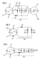
- FIG. 1 shows a first embodiment of the arrangement according to the invention.
- FIG. 2 shows a second embodiment of the arrangement according to the invention.
- FIG. 3 shows a third embodiment of the arrangement according to the invention.
- FIG. 4 shows a fourth embodiment of the arrangement according to the invention.
- FIG. 5 shows the arrangement described above for detuning a reception antenna of a local coil according to the prior art.
- FIG. 1 shows a first embodiment of the arrangement according to the invention with what is known as a loop antenna LA as a reception antenna.
- the reception antenna LA shows four capacitances C 1 through C 4 that are fashioned to shorten the reception antenna LA.
- a first capacitor C 1 together with a first inductance L 11 forms a block circuit that, together with a first diode D 11 , a second diode D 12 and a second inductance L 12 , forms a detuning circuit VSS.
- the first diode D 11 , the second diode D 12 as well as the second inductance L 12 are connected in parallel to one another, wherein the two diodes D 11 , D 12 are additionally connected or, respectively, arranged inverse to one another.
- This parallel circuit is connected on the input side with a first end of the first capacitor C 1 while the parallel circuit is connected at the output side via the first inductance L 11 with a second end of the first capacitor C 1 .
- magnetic resonance signals with a bandwidth BMR are received via the reception antenna LA.
- These received magnetic resonance signals are induced by a transmission signal that is radiated towards the patient during a transmission phase via a transmission antenna (not shown here).
- auxiliary signal HFS has a frequency f HFS that is located just outside the bandwidth B MR of the transmission signal used for examination.
- the auxiliary signal HFS is received via the reception antenna LA. Either the first diode D 11 or the second diode D 12 is switched through by the auxiliary signal HFS, such that the first inductance L 11 together with the first capacitance C 1 forms a high-resistance block circuit.
- the detuning circuit VSS is therefore detuned.
- the second inductance L 12 serves to discharge residual voltages of the two diodes D 11 and D 12 .
- FIG. 2 shows a second embodiment of the arrangement according to the invention, with a loop antenna LA as a reception antenna.
- the reception antenna LA shows four capacitances C 1 through C 4 that are fashioned to shorten the reception antenna LA.
- a first capacitor C 1 together with a first inductance L 21 forms a block circuit that, together with a first diode D 21 , a second diode D 22 and a second inductance L 22 , forms a detuning circuit VSS.
- the first diode D 21 , the second diode D 22 as well as the second inductance L 22 are thereby connected in parallel to one another, wherein the two diodes D 21 , D 22 are additionally connected or, respectively, arranged inverse to one another.
- This parallel circuit is connected on the input side with a first end of the first capacitor C 1 while the parallel circuit is connected at the output side via the first inductance L 21 with a second end of the first capacitor C 1 .
- magnetic resonance signals with a bandwidth BMR are received via the reception antenna LA.
- These received magnetic resonance signals are induced by a transmission signal that is radiated towards the patient during a transmission phase by a transmission antenna (not shown).
- auxiliary signal HFS has a frequency f HFS that is located just outside the bandwidth BMR of the transmission signal used for examination.
- the auxiliary signal HFS is received via an auxiliary antenna HA.
- the auxiliary antenna HA here is exemplarily designed as a loop antenna and contains a first capacitance CS 21 and a second capacitance CS 22 for antenna shortening.
- the auxiliary antenna HA is wired for coupling or connection with the detuning circuit VSS such that the first terminal of the first capacitance C 1 is connected with a second terminal of the capacitance CS 21 while the second terminal of the first capacitance C 1 is connected via the inductance L 21 with a first terminal of the capacitance CS 21 .
- Either the first diode D 21 or the second diode D 22 is switched through by the auxiliary signal HFS, such that the first inductance L 21 together with the first capacitance C 1 forms a high-resistance block circuit.
- the detuning circuit VSS is therefore detuned.
- the second inductance L 22 serves to discharge residual voltages of the two diodes D 21 and D 22 .
- the advantage of this auxiliary antenna embodiment lies in that the actual reception antenna LA does not have to be modified with regard to its radio reception properties because the auxiliary signal reception is carried out independently via the auxiliary antenna HA.
- FIG. 3 shows a variant (relative to FIG. 2 ) of the arrangement according to the invention as a third embodiment of the invention.
- a first capacitor C 1 of the reception antenna LA forms a detuning circuit VSS together with a first inductance L 31 , a first diode D 31 , a second diode D 32 and a second inductance L 32 .
- the first diode D 31 , the second diode D 32 as well as the second inductance L 32 are thereby connected in parallel to one another, wherein the two diodes D 31 , D 32 are additionally connected or, respectively, arranged inverse to one another.
- This parallel circuit is connected on the input side via a ⁇ /4 phase shifter with a first end of the first capacitor C 1 , while the parallel circuit is connected at the output side via the ⁇ /4 phase shifter and via the first inductance L 31 with a second end of the first capacitor C 1 .
- the ⁇ /4 phase shifter contains two capacitances C 36 and C 37 in a shunt arm in the form of a T-circuit as well as an inductance L 33 in a series arm.
- the first end of the capacitance C 1 is connected via the two capacitances C 36 and C 37 with the input of the parallel circuit.
- the first end of the capacitance C 1 is connected via the capacitance C 36 , the inductance L 33 and the first inductance L 31 with the second end of the capacitance C 1 .
- the second end of the capacitance C 1 is connected via the first inductance L 31 with the output of the parallel circuit.
- the auxiliary signal HFS used as a control signal is received via an auxiliary antenna HA.
- the auxiliary antenna HA here is exemplarily designed as a loop antenna and contains a first capacitance CS 31 and a second capacitance CS 32 for antenna shortening.
- the auxiliary antenna HA is wired for coupling or, respectively, connection with the detuning circuit VSS such that the first terminal of the first capacitance C 1 is connected via the two capacitances C 36 and C 37 with a second terminal of the capacitance CS 31 while the second terminal of the first capacitance C 1 is connected via the inductance L 31 with a first terminal of the capacitance CS 31 .
- the second inductance L 32 serves to discharge residual voltages of the two diodes D 31 and D 32 .
- the two diodes D 31 and D 32 are not switched through and thus form a radio-frequency open circuit at the ⁇ /4 transformer.
- This open circuit is transformed via the ⁇ /4 transformer into a radio-frequency short in the direction of the reception antenna LA so that the detuning circuit VSS is detuned via the capacitance C 1 and via the inductance L 31 .
- the capacitance C 1 and the inductance L 31 form a high-resistance block circuit.
- the auxiliary signal HFS is transferred and received via the auxiliary antenna HA, either the diode D 31 or the diode D 32 is switched through so that a radio-frequency short is formed at the ⁇ /4 transformer.
- This short is transformed via the lamdat/4 transformer into a radio-frequency open circuit in the direction of the reception antenna LA so that the detuning circuit VSS is tuned.
- the capacitance C 1 is decoupled from the inductance L 31 ; the block circuit cannot act via the open circuit.
- the detuning circuit VSS here is basically detuned.
- the detuning circuit VSS is essentially deactivated only given the transmission of the auxiliary signal HFS, such that the reception antenna LA is ready for operation.
- the auxiliary signal HFS is correspondingly not transmitted during the transmission phase but rather during the duration of a desired acquisition phase.
- FIG. 4 shows a fourth embodiment of the arrangement according to the invention, with a loop antenna LA as a reception antenna.
- the reception antenna LA shows four capacitances C 1 through C 4 that are fashioned to shorten the reception antenna LA.
- a first capacitor C 1 together with a first inductance L 41 , a first diode D 42 , a second diode D 43 , a second inductance L 42 and a third inductance L 43 , forms a detuning circuit VSS.
- the first diode D 42 is a PIN diode while the second diode D 43 is designed as a rectifier diode.
- the first diode D 42 and the second inductance L 42 are connected in series.
- the second diode D 43 and the third inductance L 43 are connected in series.
- Both series circuits are in turn connected in parallel with one another, wherein the two diodes D 42 , D 43 are additionally connected or, respectively, arranged inverse to one another.
- the parallel circuit is connected on the input side via the first inductance L 41 with a first end of the first capacitor C 1 , while the parallel circuit is connected at the output side with a second end of the first capacitor C 1 .
- magnetic resonance signals with a bandwidth BMR are received via the reception antenna LA.
- These received magnetic resonance signals are induced by a transmission signal that is radiated towards the patient via a transmission antenna (not shown here) during a transmission phase.
- auxiliary signal HFS has a frequency f HFS that is located just outside the bandwidth BMR of the transmission signal used for examination.
- the auxiliary signal HFS is received via the reception antenna LA. Either the first diode D 42 or the second diode D 43 is switched through by the auxiliary signal HFS, such that the first inductance L 41 together with the first capacitance C 1 forms a high-resistance block circuit.
- the detuning circuit VSS is therefore detuned.
- the parallel connection described above of the first series circuit with the elements L 42 and D 42 and the second series circuit with the elements L 43 and D 43 can seamlessly replace the parallel connection of the elements D 11 , D 12 and L 12 described in FIG. 1 .
- the described embodiments in particular have the advantage that a control signal HFS received with a low amplitude causes a switching of the oscillating circuit.
Abstract
Description
Claims (9)
Applications Claiming Priority (3)
| Application Number | Priority Date | Filing Date | Title |
|---|---|---|---|
| DE102008014751 | 2008-03-18 | ||
| DE102008014751.6A DE102008014751B4 (en) | 2008-03-18 | 2008-03-18 | Method for operating an arrangement for detuning a receiving antenna in a local coil |
| DE102008014751.6 | 2008-03-18 |
Publications (2)
| Publication Number | Publication Date |
|---|---|
| US20090237081A1 US20090237081A1 (en) | 2009-09-24 |
| US8085048B2 true US8085048B2 (en) | 2011-12-27 |
Family
ID=41051255
Family Applications (1)
| Application Number | Title | Priority Date | Filing Date |
|---|---|---|---|
| US12/404,793 Active 2030-01-23 US8085048B2 (en) | 2008-03-18 | 2009-03-16 | Arrangement to detune a reception antenna in a local coil |
Country Status (3)
| Country | Link |
|---|---|
| US (1) | US8085048B2 (en) |
| CN (1) | CN101539614B (en) |
| DE (1) | DE102008014751B4 (en) |
Cited By (5)
| Publication number | Priority date | Publication date | Assignee | Title |
|---|---|---|---|---|
| US9903926B2 (en) | 2012-06-26 | 2018-02-27 | Siemens Aktiengesellschaft | Determination of communication latency in magnetic resonance tomography systems |
| US20190049533A1 (en) * | 2017-08-09 | 2019-02-14 | Siemens Healthcare Gmbh | Sheath wave barrier-free connecting lead and magnetic resonance tomograph with connecting lead |
| US10274560B2 (en) | 2013-07-22 | 2019-04-30 | Siemens Aktiengesellschaft | Use of a plurality of TX coils |
| US10416252B2 (en) | 2014-07-01 | 2019-09-17 | Koninklijke Philips N.V. | MR receive coil with detune circuit and energy harvesting circuit |
| EP4253980A1 (en) * | 2022-03-29 | 2023-10-04 | Koninklijke Philips N.V. | Tunable radio frequency coil assembly and magnetic resonance system comprising the rf coil assembly |
Families Citing this family (12)
| Publication number | Priority date | Publication date | Assignee | Title |
|---|---|---|---|---|
| DE102008014751B4 (en) * | 2008-03-18 | 2015-01-15 | Siemens Aktiengesellschaft | Method for operating an arrangement for detuning a receiving antenna in a local coil |
| WO2011122084A1 (en) * | 2010-03-31 | 2011-10-06 | 株式会社 日立製作所 | Rf coil and magnetic resonance imaging device |
| CN103547937B (en) * | 2011-05-23 | 2016-09-21 | 皇家飞利浦有限公司 | FET as the detuned circuit for MRI RF coil switchs |
| DE102011083599B3 (en) * | 2011-09-28 | 2013-03-28 | Siemens Aktiengesellschaft | Acquisition of calibration data for a magnetic resonance system |
| CN103630858B (en) * | 2012-08-23 | 2018-09-14 | 西门子(深圳)磁共振有限公司 | A kind of shoulder coil and transmitting coil of magnetic resonance system |
| CN103969609B (en) * | 2013-01-30 | 2016-12-28 | 西门子(深圳)磁共振有限公司 | A kind of local coil and magnetic resonance imaging system |
| DE102013213377B3 (en) * | 2013-07-09 | 2014-07-03 | Siemens Aktiengesellschaft | Local coil for MRI system, has diode that is connected to antenna between two connection points in the space formed between two portions of antenna |
| CN106646298B (en) * | 2015-10-28 | 2019-05-24 | 西门子(深圳)磁共振有限公司 | A kind of body coil and magnetic resonance imaging system |
| WO2019013857A1 (en) * | 2017-04-28 | 2019-01-17 | Raytheon Company | Diode-based transmitter and receiver detuning circuits |
| CN107632278A (en) * | 2017-08-31 | 2018-01-26 | 上海联影医疗科技有限公司 | Magnetic resonance system and MR imaging method |
| DE102019220054A1 (en) * | 2019-12-18 | 2021-06-24 | Siemens Healthcare Gmbh | Device and method for real-time monitoring and control of local coils |
| CN114114113A (en) * | 2020-08-31 | 2022-03-01 | 西门子(深圳)磁共振有限公司 | Receiving coil and magnetic resonance imaging apparatus |
Citations (20)
| Publication number | Priority date | Publication date | Assignee | Title |
|---|---|---|---|---|
| US5666055A (en) * | 1995-10-02 | 1997-09-09 | Jones; Randall W. | Surface coil system for a single channel NMR receiver |
| US5903151A (en) * | 1996-08-29 | 1999-05-11 | Siemens Aktiengesellschaft | Local antenna arrangement for a magnetic resonance apparatus |
| US6710597B2 (en) | 2001-04-11 | 2004-03-23 | Siemens Aktiengesellschaft | Magnetic resonance tomography apparatus and method for operating same employing an electrostatic relay |
| US20040124838A1 (en) * | 2001-03-30 | 2004-07-01 | Duerk Jeffrey L | Wireless detuning of a resonant circuit in an mr imaging system |
| US20070167726A1 (en) * | 2005-12-30 | 2007-07-19 | Orhan Unal | Multi-mode medical device system and methods of manufacturing and using same |
| US20070182409A1 (en) * | 2004-07-15 | 2007-08-09 | Koninklijke Philips Electronics N.V. | Wireless mr receiving coil system |
| US20070268018A1 (en) | 2003-12-08 | 2007-11-22 | Koninklijke Philips Electronics Nv | Circuit Arrangement for Detuning a Resonant Circuit of an Mr Apparatus |
| US20080114235A1 (en) * | 2006-11-15 | 2008-05-15 | Wisconsin Alumni Research Foundation | System and method for simultaneous 3DPR device tracking and imaging under MR-guidance for therapeutic endovascular interventions |
| US20080183070A1 (en) * | 2007-01-29 | 2008-07-31 | Wisconsin Alumni Research Foundation | Multi-mode medical device system with thermal ablation capability and methods of using same |
| US7417433B2 (en) | 2005-05-17 | 2008-08-26 | Siemens Aktiengesellschaft | Method, examination apparatus and antenna array for magnetic resonance data acquisition |
| US20080208031A1 (en) * | 2007-02-28 | 2008-08-28 | Wisconsin Alumni Research Foundation | Voltage standing wave suppression for MR-guided therapeutic interventions |
| US20080272786A1 (en) * | 2004-06-25 | 2008-11-06 | Koninklijke Philips Electronics N.V. | Integrated Power Supply for Surface Coils |
| US20090237081A1 (en) * | 2008-03-18 | 2009-09-24 | Stephan Biber | Arrangement to detune a reception antenna in a local coil |
| US20090278537A1 (en) * | 2006-06-30 | 2009-11-12 | Koninklijke Philips Electronics N. V. | Radio-frequency surface coils comprising on-board digital receiver circuit |
| US20100188208A1 (en) * | 2006-05-12 | 2010-07-29 | Koninklijke Philips Electronics N. V. | Wireless patient parameter sensors for use in mri |
| US20100256481A1 (en) * | 2007-09-27 | 2010-10-07 | Mareci Thomas H | Method and Apparatus for Providing a Wireless Multiple-Frequency MR Coil |
| US20100277175A1 (en) * | 2006-08-15 | 2010-11-04 | Koninklijke Philips Electronics N.V. | Tunable and/or detunable mr receive coil arrangements |
| US20100294829A1 (en) * | 2007-01-10 | 2010-11-25 | Ethicon Endo-Surgery, Inc. | Surgical instrument with wireless communication between control unit and sensor transponders |
| US20100301862A1 (en) * | 2009-05-29 | 2010-12-02 | Tropp James S | Dual-frequency coil array for a magnetic resonance imaging (mri) system |
| US20110218402A1 (en) * | 2008-11-18 | 2011-09-08 | Olympus Corporation | Capsule-type medical device, power supply apparatus, and power supply system |
-
2008
- 2008-03-18 DE DE102008014751.6A patent/DE102008014751B4/en not_active Expired - Fee Related
-
2009
- 2009-03-10 CN CN2009101266622A patent/CN101539614B/en not_active Expired - Fee Related
- 2009-03-16 US US12/404,793 patent/US8085048B2/en active Active
Patent Citations (22)
| Publication number | Priority date | Publication date | Assignee | Title |
|---|---|---|---|---|
| US5666055A (en) * | 1995-10-02 | 1997-09-09 | Jones; Randall W. | Surface coil system for a single channel NMR receiver |
| US5903151A (en) * | 1996-08-29 | 1999-05-11 | Siemens Aktiengesellschaft | Local antenna arrangement for a magnetic resonance apparatus |
| US20040124838A1 (en) * | 2001-03-30 | 2004-07-01 | Duerk Jeffrey L | Wireless detuning of a resonant circuit in an mr imaging system |
| US6710597B2 (en) | 2001-04-11 | 2004-03-23 | Siemens Aktiengesellschaft | Magnetic resonance tomography apparatus and method for operating same employing an electrostatic relay |
| US20070268018A1 (en) | 2003-12-08 | 2007-11-22 | Koninklijke Philips Electronics Nv | Circuit Arrangement for Detuning a Resonant Circuit of an Mr Apparatus |
| US20080272786A1 (en) * | 2004-06-25 | 2008-11-06 | Koninklijke Philips Electronics N.V. | Integrated Power Supply for Surface Coils |
| US7602187B2 (en) * | 2004-06-25 | 2009-10-13 | Koninklijke Philips Electronics N.V. | Integrated power supply for surface coils |
| US20070182409A1 (en) * | 2004-07-15 | 2007-08-09 | Koninklijke Philips Electronics N.V. | Wireless mr receiving coil system |
| US7443165B2 (en) * | 2004-07-15 | 2008-10-28 | Koninklijke Philips Electronics N.V. | Wireless MR receiving coil system |
| US7417433B2 (en) | 2005-05-17 | 2008-08-26 | Siemens Aktiengesellschaft | Method, examination apparatus and antenna array for magnetic resonance data acquisition |
| US20070167726A1 (en) * | 2005-12-30 | 2007-07-19 | Orhan Unal | Multi-mode medical device system and methods of manufacturing and using same |
| US20100188208A1 (en) * | 2006-05-12 | 2010-07-29 | Koninklijke Philips Electronics N. V. | Wireless patient parameter sensors for use in mri |
| US20090278537A1 (en) * | 2006-06-30 | 2009-11-12 | Koninklijke Philips Electronics N. V. | Radio-frequency surface coils comprising on-board digital receiver circuit |
| US20100277175A1 (en) * | 2006-08-15 | 2010-11-04 | Koninklijke Philips Electronics N.V. | Tunable and/or detunable mr receive coil arrangements |
| US20080114235A1 (en) * | 2006-11-15 | 2008-05-15 | Wisconsin Alumni Research Foundation | System and method for simultaneous 3DPR device tracking and imaging under MR-guidance for therapeutic endovascular interventions |
| US20100294829A1 (en) * | 2007-01-10 | 2010-11-25 | Ethicon Endo-Surgery, Inc. | Surgical instrument with wireless communication between control unit and sensor transponders |
| US20080183070A1 (en) * | 2007-01-29 | 2008-07-31 | Wisconsin Alumni Research Foundation | Multi-mode medical device system with thermal ablation capability and methods of using same |
| US20080208031A1 (en) * | 2007-02-28 | 2008-08-28 | Wisconsin Alumni Research Foundation | Voltage standing wave suppression for MR-guided therapeutic interventions |
| US20100256481A1 (en) * | 2007-09-27 | 2010-10-07 | Mareci Thomas H | Method and Apparatus for Providing a Wireless Multiple-Frequency MR Coil |
| US20090237081A1 (en) * | 2008-03-18 | 2009-09-24 | Stephan Biber | Arrangement to detune a reception antenna in a local coil |
| US20110218402A1 (en) * | 2008-11-18 | 2011-09-08 | Olympus Corporation | Capsule-type medical device, power supply apparatus, and power supply system |
| US20100301862A1 (en) * | 2009-05-29 | 2010-12-02 | Tropp James S | Dual-frequency coil array for a magnetic resonance imaging (mri) system |
Cited By (6)
| Publication number | Priority date | Publication date | Assignee | Title |
|---|---|---|---|---|
| US9903926B2 (en) | 2012-06-26 | 2018-02-27 | Siemens Aktiengesellschaft | Determination of communication latency in magnetic resonance tomography systems |
| US10274560B2 (en) | 2013-07-22 | 2019-04-30 | Siemens Aktiengesellschaft | Use of a plurality of TX coils |
| US10416252B2 (en) | 2014-07-01 | 2019-09-17 | Koninklijke Philips N.V. | MR receive coil with detune circuit and energy harvesting circuit |
| US20190049533A1 (en) * | 2017-08-09 | 2019-02-14 | Siemens Healthcare Gmbh | Sheath wave barrier-free connecting lead and magnetic resonance tomograph with connecting lead |
| US10809327B2 (en) * | 2017-08-09 | 2020-10-20 | Siemens Healthcare Gmbh | Sheath wave barrier-free connecting lead and magnetic resonance tomograph with connecting lead |
| EP4253980A1 (en) * | 2022-03-29 | 2023-10-04 | Koninklijke Philips N.V. | Tunable radio frequency coil assembly and magnetic resonance system comprising the rf coil assembly |
Also Published As
| Publication number | Publication date |
|---|---|
| DE102008014751A1 (en) | 2009-10-08 |
| CN101539614B (en) | 2013-10-02 |
| DE102008014751B4 (en) | 2015-01-15 |
| US20090237081A1 (en) | 2009-09-24 |
| CN101539614A (en) | 2009-09-23 |
Similar Documents
| Publication | Publication Date | Title |
|---|---|---|
| US8085048B2 (en) | Arrangement to detune a reception antenna in a local coil | |
| US5903150A (en) | Antenna system for NMR and MRI apparatus | |
| US7501823B2 (en) | Cylindrical magnetic resonance antenna | |
| JP6210976B2 (en) | FET switch as detuning circuit for MRIRF coil | |
| US7385399B2 (en) | Radio-frequency antenna arrangement for acquisition of a magnetic resonance signal | |
| US6160400A (en) | Radio-frequency receiver unit for a magnetic resonance apparatus | |
| US6747452B1 (en) | Decoupling circuit for magnetic resonance imaging local coils | |
| US8237442B2 (en) | Magnetic resonance antenna | |
| US6850067B1 (en) | Transmit mode coil detuning for MRI systems | |
| US10557900B2 (en) | Body coil having a pre-amplification unit configured to provide a detuning effect | |
| US20130207660A1 (en) | Rf antenna arrangement for mri comprising a trap circuit | |
| US7746073B2 (en) | Magnetic resonance imaging system | |
| US20230078150A1 (en) | Double-resonant coil, array of double-resonant coils, and use thereof | |
| US20230261375A1 (en) | Transmission line coupled antenna and detuning circuit | |
| US7663370B2 (en) | Arrangement to control antenna elements | |
| US9625554B2 (en) | Electronic interface for NMR receiver resonators | |
| US7053615B2 (en) | Magnetic resonance system | |
| US11668775B2 (en) | Integrated active detuning for magnetic resonance imaging | |
| US7068035B2 (en) | Magnetic resonance apparatus with a detunable RF resonator | |
| US10094894B2 (en) | Transmitting and/or receiving MRI signals for a MRI examination | |
| US20020060568A1 (en) | Inductively coupled reception coil arrangement for magnetic resonance tomography | |
| US20160320465A1 (en) | Detuning a mrt receive antenna | |
| JP3836416B2 (en) | RF receiving coil and magnetic resonance imaging apparatus | |
| WO2023186586A1 (en) | Tunable radio frequency coil assembly and magnetic resonance system comprising the rf coil assembly |
Legal Events
| Date | Code | Title | Description |
|---|---|---|---|
| AS | Assignment |
Owner name: SIEMENS AKTIENGESELLSCHAFT, GERMANY Free format text: ASSIGNMENT OF ASSIGNORS INTEREST;ASSIGNORS:BIBER, STEPHAN;GREIM, HELMUT;STAPF, JOERG CHRISTOPHER;REEL/FRAME:022401/0858;SIGNING DATES FROM 20090306 TO 20090311 Owner name: SIEMENS AKTIENGESELLSCHAFT, GERMANY Free format text: ASSIGNMENT OF ASSIGNORS INTEREST;ASSIGNORS:BIBER, STEPHAN;GREIM, HELMUT;STAPF, JOERG CHRISTOPHER;SIGNING DATES FROM 20090306 TO 20090311;REEL/FRAME:022401/0858 |
|
| STCF | Information on status: patent grant |
Free format text: PATENTED CASE |
|
| FPAY | Fee payment |
Year of fee payment: 4 |
|
| AS | Assignment |
Owner name: SIEMENS HEALTHCARE GMBH, GERMANY Free format text: ASSIGNMENT OF ASSIGNORS INTEREST;ASSIGNOR:SIEMENS AKTIENGESELLSCHAFT;REEL/FRAME:039271/0561 Effective date: 20160610 |
|
| MAFP | Maintenance fee payment |
Free format text: PAYMENT OF MAINTENANCE FEE, 8TH YEAR, LARGE ENTITY (ORIGINAL EVENT CODE: M1552); ENTITY STATUS OF PATENT OWNER: LARGE ENTITY Year of fee payment: 8 |
|
| MAFP | Maintenance fee payment |
Free format text: PAYMENT OF MAINTENANCE FEE, 12TH YEAR, LARGE ENTITY (ORIGINAL EVENT CODE: M1553); ENTITY STATUS OF PATENT OWNER: LARGE ENTITY Year of fee payment: 12 |
|
| AS | Assignment |
Owner name: SIEMENS HEALTHINEERS AG, GERMANY Free format text: ASSIGNMENT OF ASSIGNORS INTEREST;ASSIGNOR:SIEMENS HEALTHCARE GMBH;REEL/FRAME:066088/0256 Effective date: 20231219 |