US8085857B1 - Digital-compatible multi-state-sense input - Google Patents
Digital-compatible multi-state-sense input Download PDFInfo
- Publication number
- US8085857B1 US8085857B1 US10/947,890 US94789004A US8085857B1 US 8085857 B1 US8085857 B1 US 8085857B1 US 94789004 A US94789004 A US 94789004A US 8085857 B1 US8085857 B1 US 8085857B1
- Authority
- US
- United States
- Prior art keywords
- signal
- state
- input line
- driven
- driver
- Prior art date
- Legal status (The legal status is an assumption and is not a legal conclusion. Google has not performed a legal analysis and makes no representation as to the accuracy of the status listed.)
- Expired - Fee Related, expires
Links
Images


Classifications
-
- H—ELECTRICITY
- H04—ELECTRIC COMMUNICATION TECHNIQUE
- H04B—TRANSMISSION
- H04B3/00—Line transmission systems
-
- H—ELECTRICITY
- H04—ELECTRIC COMMUNICATION TECHNIQUE
- H04L—TRANSMISSION OF DIGITAL INFORMATION, e.g. TELEGRAPHIC COMMUNICATION
- H04L25/00—Baseband systems
- H04L25/02—Details ; arrangements for supplying electrical power along data transmission lines
- H04L25/0264—Arrangements for coupling to transmission lines
- H04L25/0292—Arrangements specific to the receiver end
-
- H—ELECTRICITY
- H04—ELECTRIC COMMUNICATION TECHNIQUE
- H04L—TRANSMISSION OF DIGITAL INFORMATION, e.g. TELEGRAPHIC COMMUNICATION
- H04L25/00—Baseband systems
- H04L25/38—Synchronous or start-stop systems, e.g. for Baudot code
- H04L25/40—Transmitting circuits; Receiving circuits
-
- H—ELECTRICITY
- H04—ELECTRIC COMMUNICATION TECHNIQUE
- H04L—TRANSMISSION OF DIGITAL INFORMATION, e.g. TELEGRAPHIC COMMUNICATION
- H04L25/00—Baseband systems
- H04L25/02—Details ; arrangements for supplying electrical power along data transmission lines
- H04L25/0264—Arrangements for coupling to transmission lines
- H04L25/028—Arrangements specific to the transmitter end
- H04L25/029—Provision of high-impedance states
Definitions
- the invention relates generally to electronic circuits. More particularly, the invention relates to sensing of multiple states for a digital signal.
- a signal may have multiple states that need to be detected in order to understand the signal.
- a signal is binary, having only two possible states. The detection of two states, which are generally high (which may be represented as “1”) or low (which may be represented as “0”), is relatively easy. In a simple example, a signal that is above a certain threshold voltage is high, while a signal that is below a certain threshold voltage is low.
- a signal having a greater number of states such as a three-state, or ternary, signal.
- the states for such a signal may be high, low, and high impedance, although three voltage levels may be used in some cases.
- a simple binary detection circuit will not be able to sense a third state, such as a high impedance state.
- a line may be precharged and then tested. Such a process assumes that the device under test is stimulated, and then the input is sensed. This assumption greatly limits the applicability of the technique to situations in which the user has control of the device driving the input since it does not allow for the continuous sense of the input to determine the high-impedance state.
- FIG. 1 is an illustration of ternary signal detection
- FIG. 2 is a flow chart illustrating an embodiment of signal detection
- FIG. 3 is a diagram of an embodiment of a circuit to provide signal detection
- FIGS. 4A and 4B are timing diagrams to illustrate an embodiment of a signal detection process
- FIGS. 5 and 6 contain sample code to simulate signal detection
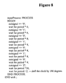
- FIGS. 7 and 8 contain sample code to define stimulus for the simulation of signal detection.
- detection of a multi-state signal is provided.
- a system detects three signal values on a signal line, which may be referred to as a ternary signal system.
- the signal may have a value of “high” or “low”, or may be undriven, a “high impedance” or “high Z” value.
- a single-ended digital I/O (input/output) system is utilized to sense when an input is not driven, and thus is in the third state.
- the signal line is alternately driven with a weak digital “1” (or “high”) and a weak digital “0” (or “low”).
- a signal history is used to determine if the input is being actively driven or is undriven.
- three separate states are sensed on a signal line using a single digital input, rather than the signal line being limited to a normal binary (“1” or “0”) input.
- An embodiment of the invention may thus be compatible with single-ended binary electrical systems such as TTL (transistor-transistor logic), LVTTL (low voltage transistor-transistor logic), CMOS (complementary metal oxide semiconductor), LVCMOS (low voltage complementary metal oxide semiconductor), and others.
- TTL transistor-transistor logic
- LVTTL low voltage transistor-transistor logic
- CMOS complementary metal oxide semiconductor
- LVCMOS low voltage complementary metal oxide semiconductor
- Ternary sensing is generally not compatible with digital I/Os because the input characteristics do not match the characteristics of digital drivers.
- sensing of three states may be accomplished using a digital input, a synchronous finite state machine (FSM), and a toggling weak driver.
- An input device under test (DUT) will provide a signal by driving the input with a logic ‘0’ (low), driving the input with a logic ‘1’ (high), or leaving the output undriven (high-impedance).
- a detection system will continually drive the input line with a weak driver that provides a signal that is easily overcome by an external driver of normal strength. The value driven by the weak driver alternates between a weak high and a weak low signal.
- the weak driver value may utilize the output of a T-type flip-flop that is driven by a clock.
- any circuit that generates a binary alternating pattern may be used in an embodiment of the invention.
- a history of the values sensed by a detector is used to determine the state of the signal on the input line.
- An input signal value can be determined using a finite state machine that operates according to the criteria provided in Table 1.
- a weak internal driver When the input is actively driven by an external driver, a weak internal driver is not able to overcome the external driver. As a result, a transition from a weak “low” to a “high” state can be determined to be a “high” signal. This is the result of the external driver overriding the signal of the weak internal driver. Similarly, a transition from a weak “high” to a “low” state can be determined to be a “low” signal.
- the action of the toggling weak driver will switch the logic level sensed by the input.
- a counter can be used to count a number of times that the weak driver has switched the logic level of the input.
- the finite state machine can determine that the input is in the undriven or “high impedance” state.
- the number of times that the input is switched will depend on, among other elements, the degree of certainty required for signal detection. The first time a signal is driven, it may coincidentally be the same as an external signal.
- the weak signal needs to be switched and the detected output needs to follow the weak driven signal for at least two consecutive clock cycles to detect a high impedance signal, but additional clock cycles may be utilized to provide a greater certainty and ensure that a glitch has not occurred in the signaling.
- FIG. 1 is an illustration of ternary signal detection.
- a detector 105 is to detect a signal 115 on a line 110 .
- the signal can be a “high” signal 120 , a “low” signal 125 , or an undriven/high impedance signal 130 .
- a weak driver 135 alternatively drives a weak “high” and a weak “low” on the line 110 .
- the detector 105 then detects the resulting signal 115 on the line 110 .
- the detector may wait a certain delay period before detecting the signal to allow transitory “ringing” in a signal to dissipate. If the detected signal is the opposite of the weakly driven signal, with a “high” detected when driving a weak “low” or a “low” detected when driving a weak “high”, then the detected signal is determined to be the state of the signal.
- the weak driver 135 toggles to the opposite state and the signal is again detected. If the detected signal now is the opposite of the weakly driven signal, then the detected signal is determined to be the state of the signal. If the detected signal follows the weakly driven signal for a certain number of repetitions, the number of repetitions being two or more, then the signal is determined to be an undriven or “high impedance” signal.
- FIG. 2 is a flow chart illustrating an embodiment of signal detection.
- a counter i is set to zero 205 .
- the operation of the counter may represent an operation of a finite state machine.
- an I/O system drives a weak “high” or “low” signal on a line 210 .
- the weak internal driver signaling may begin with either a “high” or “low” signal.
- the I/O system detects the state of the signal 215 , the I/O being required to only discern between a “high” signal value and a “low” signal value on a single line. If the detected signal does not match the weakly driven signal 220 , thus indicating that an external driver has overridden the weakly driven signal, then the signal may be deemed to be the detected logical signal 225 .
- the counter is incremented 230 . If the counter equals a value n 235 , with n being at least 2, then the signal may be deemed to be an undriven/high impedance signal 240 . If n does not equal the value n, then the weak driver is toggled 245 to produce the opposite signal and a weak signal is again driven on the line 210 . In the next iteration, the detected signal may now no longer match the weakly driven signal 220 , indicating that the signal is driven and the detected and weakly driven signals had matched coincidentally in the first iteration. If the detected and weakly driven signals again match, then the iterations continue until the counter reaches the required value.
- FIG. 3 is a diagram of an embodiment of a circuit to provide signal detection.
- the illustrated circuit is one example of a circuit for ternary signal, but other circuits can also be utilized.
- an I/O system 305 is utilized to detect the output of a device under test 310 on a line 315 .
- the signal on line 315 may be a “high” signal, a “low” signal, or a “non-driven” (or high impedance) signal.
- the device under test 310 may be any digital device, with the device here showing a driver 325 driving an output signal, with another driver 320 possibly driving the signal as in input.
- the I/O system 305 includes a component to sense a signal, such as an input buffer 330 to drive the signal from the line 315 to a logic circuit 335 .
- the logic circuit may act as a finite state machine.
- the logic circuit also receives the output of a T-type flip-flop 340 , the output of the flip-flop 340 representing an internal signal for use in signal detection.
- the output of the flip-flop 340 is input to a weak driver 345 to drive a weak signal value on the line 315 .
- the initial state of the flip-flop can arbitrarily be either “high” or “low”, and is toggled back and forth between states according to a clock clk 350 .
- the logic circuit 335 then outputs a determined signal Z_out 355 , as well as a signal logic_out 360 .
- a “high” value on Z_out 355 indicates that the sensed signal on line 315 is an undriven signal.
- a “low” value on Z-out 355 indicates that the sensed signal is a driven signal having the logical value found on logic_out 360 .
- the device under test 310 provides a signal by driving a logical signal on the line 315 or by leaving the line undriven.
- the T-type flip-flop 340 weakly drives a state on the line 315 using weak driver 345 .
- the resulting signal is received by input buffer 330 , with the resulting detected signal and the state of the flip-flop 340 being input to the logic circuit 335 . If the detected signal and the state of the flip-flop 340 are opposite signals, then the detected signal is the value of the signal on line 315 . In this case, Z-out will be “low” and the logical signal value is provided by logic_out 360 . If the detected signal and the state of the flip-flop 340 are the same, then the value of the signal is initially uncertain.
- the clock 350 then toggles the flip-flop 340 and the output of the flip-flop 340 and the detected signal amplified by amplifier 330 are again input to the logic circuit 335 . If the detected signal and the state of the flip-flop 340 are now opposite signals, the detected signal is the signal value, and the logical signal value is provided on logic_out 360 . If the detected signal and the state of the flip-flop 340 are again the same, then the value of the signal may be deemed to be undriven. In another embodiment, the flip-flop 340 is again toggled and the process continues for one or more additional iterations to provide more certainty in the value of the signal. If the signal is deemed to be undriven, then Z-out will be “high” to indicate that a high-impedance signal has been sensed.
- FIGS. 4A and 4B are timing diagrams to illustrate an embodiment of a signal detection process.
- the timing diagrams illustrate the operation of a simulated circuit and thus the signals provided by an operating system may vary in appearance.
- FIG. 4A there is illustrated a clock signal “clk” 405 , a signal “outsignal” 410 representing a signal on a common net, a signal “logicsignal” 415 to indicate a high or low logical signal value, and a signal “highzsignal” 420 to indicate the presence of a high impedance signal.
- the signal “clk” 405 represents an internal clock signal.
- the signal “highzsignal” 420 is used to indicate whether the signal value that is sensed is a high-impedance signal or is a valid logical level. When “highzsignal” 420 is high (“1”) this indicates that a sensed signal value is high-impedance. When “highzsignal” 420 is low (“0”) this indicates that the logic level of the signal value sensed is found on the signal “logicsignal” 415 .
- the signal “logicsignal” 415 tracks the signal “outsignal” 410 on the common net between the devices, indicating that an external device driving is driving the signal.
- a finite state machine can determine the value of the driven signal to be the value of the detected signal.
- the weak driver is able to successfully drive the input to alternate high and low states, as can be seen in the second portion of the timing diagram 430 .
- the finite state machine determines the input is in the high-impedance state, which is indicated by “highzsignal” transitioning to a “high” (“1”) value.
- FIG. 4B illustrates a transition from a high-impedance state to a driven state.
- FIG. 4B again illustrates a clock signal “clk” 430 , a signal “outsignal” 435 representing a signal on a common net, a logic signal “logicsignal” 440 to indicate a high or low signal value, and a high impedance signal “highzsignal” 445 to indicate the presence of a high impedance signal.
- the system is in a high-impedance state at the leftmost time shown in the waveform, as seen in a first portion 455 . This status is indicated by the value of ‘1’ for “highzsignal”.
- the common net “outsignal” is driven by the external device, and the invention's FSM leaves the high-impedance state. This is shown in a second portion 460 .
- the change is indicated by the high-to-low transition of “highzsignal” followed by the matching of “logicsignal” to the common (and now externally driven) net “outsignal”.
- FIGS. 5 and 6 contain sample code in VHDL (VHSIC [Very-High-Speed Integrated Circuit] Hardware Description Language) to simulate signal detection.
- the sample code can be used to illustrate system operation, such as in generating the timing diagrams provided in FIGS. 4A and 4B .
- FIG. 5 the cases in which the line is driven are initially handled. When the input signal “insig” is detected as “0” and the “weakdriver” signal is high, then “highZ_out” is “0” (indicating that a driven signal is present) and the sensed signal provided on logic_out is “0”, indicating that the received signal is a “0” value.
- FIG. 5 provides for handling cases in which the detected signal is aligned with the weak driver, thus either a “0” signal and a low weak driver or a “1” signal and a high weak driver.
- FIG. 6 then continues with cases in which the detected signal matches the weak driver signal.
- a counter highZ_count is incremented each time the detected signal “insig” matches the “weakdriver” value.
- the weak driver has toggled the signal value three times, and thus “highZ_count” has reached a binary value of “11”, then the signal highZ_out becomes a value of “1”, indicating that the detected signal is a high impedance signal.
- FIGS. 7 and 8 contain sample code to define the stimulus for signal detection in the VHDL circuit simulation.
- the present invention includes various processes. Certain processes of the present invention may be performed by hardware components or may be embodied in machine-executable instructions, which may be used to cause a general-purpose or special-purpose processor or logic circuits programmed with the instructions to perform the processes. Alternatively, the processes may be performed by a combination of hardware and software.
- Certain portions of the present invention may be provided as a computer program product, which may include a machine-readable medium having stored thereon instructions, which may be used to program a computer (or other electronic devices) to perform a process according to the present invention.
- the machine-readable medium may include, but is not limited to, floppy diskettes, optical disks, CD-ROMs, and magneto-optical disks, ROMs, RAMS, EPROMs, EEPROMs, magnet or optical cards, flash memory, or other type of media/machine-readable medium suitable for storing electronic instructions.
- certain portions of the present invention may also be downloaded as a computer program product, wherein the program may be transferred from a remote computer to a requesting computer by way of data signals embodied in a carrier wave or other propagation medium via a communication link (e.g., a modem or network connection).
- a communication link e.g., a modem or network connection
Abstract
Description
| TABLE 1 | ||
| Value driven | Value sensed | |
| on line | on line | Action |
| Weak low | High | FSM determines “high” state |
| Weak high | Low | FSM determines “low” state |
| Weak low | Low | Increment impedance counter in FSM |
| Weak high | High | Increment impedance counter in FSM |
Claims (13)
Priority Applications (1)
| Application Number | Priority Date | Filing Date | Title |
|---|---|---|---|
| US10/947,890 US8085857B1 (en) | 2003-09-25 | 2004-09-22 | Digital-compatible multi-state-sense input |
Applications Claiming Priority (2)
| Application Number | Priority Date | Filing Date | Title |
|---|---|---|---|
| US50667703P | 2003-09-25 | 2003-09-25 | |
| US10/947,890 US8085857B1 (en) | 2003-09-25 | 2004-09-22 | Digital-compatible multi-state-sense input |
Publications (1)
| Publication Number | Publication Date |
|---|---|
| US8085857B1 true US8085857B1 (en) | 2011-12-27 |
Family
ID=45349874
Family Applications (1)
| Application Number | Title | Priority Date | Filing Date |
|---|---|---|---|
| US10/947,890 Expired - Fee Related US8085857B1 (en) | 2003-09-25 | 2004-09-22 | Digital-compatible multi-state-sense input |
Country Status (1)
| Country | Link |
|---|---|
| US (1) | US8085857B1 (en) |
Citations (48)
| Publication number | Priority date | Publication date | Assignee | Title |
|---|---|---|---|---|
| US3610954A (en) | 1970-11-12 | 1971-10-05 | Motorola Inc | Phase comparator using logic gates |
| US3925614A (en) | 1973-09-28 | 1975-12-09 | Philips Corp | Receiver for the reception of pulse signals transmitted by means of frequency shift modulation |
| US3938184A (en) | 1975-03-21 | 1976-02-10 | The United States Of America As Represented By The Secretary Of The Navy | Digital flutter reduction system |
| US4128812A (en) | 1977-08-09 | 1978-12-05 | The United States Of America As Represented By The Secretary Of The Army | Phase discriminator |
| US4218771A (en) | 1978-12-04 | 1980-08-19 | Rockwell International Corporation | Automatic clock positioning circuit for a digital data transmission system |
| US4330863A (en) | 1978-07-07 | 1982-05-18 | Wright Simon C M | Demodulator arrangement |
| US4339731A (en) | 1980-06-05 | 1982-07-13 | Rockwell International Corporation | Stable, fast slew, phase locked loop |
| US4520489A (en) | 1983-08-15 | 1985-05-28 | Rockwell International Corporation | Decision feedback equalizing apparatus |
| US4535459A (en) | 1983-05-26 | 1985-08-13 | Rockwell International Corporation | Signal detection apparatus |
| US4538283A (en) | 1983-07-26 | 1985-08-27 | Rockwell International Corporation | Adaptive equalizer suitable for use with fiber optics |
| US4555789A (en) | 1983-07-26 | 1985-11-26 | Rockwell International Corporation | Equalizer circuit suitable for adaptive use with fiber optics |
| US4561098A (en) | 1981-09-29 | 1985-12-24 | U.S. Philips Corporation | Receiver for FFSK modulated data signals |
| US4565976A (en) | 1983-08-05 | 1986-01-21 | Advanced Micro Devices, Inc. | Interruptable voltage-controlled oscillator and phase-locked loop using same |
| US4584695A (en) | 1983-11-09 | 1986-04-22 | National Semiconductor Corporation | Digital PLL decoder |
| US4587653A (en) | 1983-09-30 | 1986-05-06 | Rockwell International Corporation | Circuit for controllable generation of pseudoerrors in bit processing |
| FR2573592A1 (en) | 1984-11-20 | 1986-05-23 | Bull Sa | Oscillator circuit phase-locked to a signal of predetermined frequency |
| FR2588433A1 (en) | 1985-10-09 | 1987-04-10 | Bull Sa | Filter with switchable transfer function and phase-locking loop containing the said filter |
| US4686481A (en) | 1985-02-01 | 1987-08-11 | Advanced Micro Devices, Inc. | Phase detector apparatus including charge pump means |
| US4724401A (en) | 1987-04-23 | 1988-02-09 | Rockwell International Corporation | Adaptive oscillator apparatus for use in a phase-lock loop |
| US4744084A (en) * | 1986-02-27 | 1988-05-10 | Mentor Graphics Corporation | Hardware modeling system and method for simulating portions of electrical circuits |
| US4788512A (en) | 1987-06-05 | 1988-11-29 | Rockwell International Corporation | Gain maintenance apparatus for use with a high gain amplifier incorporated in a closed loop feedback system |
| US4811361A (en) | 1986-10-30 | 1989-03-07 | Bull, S.A. | Method and apparatus for transmission of digital data |
| US4821293A (en) | 1987-05-20 | 1989-04-11 | Sony Corporation | Digital phase locked loop circuit |
| US4884041A (en) | 1987-06-05 | 1989-11-28 | Hewlett-Packard Company | Fully integrated high-speed voltage controlled ring oscillator |
| US4926447A (en) | 1988-11-18 | 1990-05-15 | Hewlett-Packard Company | Phase locked loop for clock extraction in gigabit rate data communication links |
| US4940904A (en) * | 1988-05-23 | 1990-07-10 | Industrial Technology Research Institute | Output circuit for producing positive and negative pulses at a single output terminal |
| US5015970A (en) | 1990-02-15 | 1991-05-14 | Advanced Micro Devices, Inc. | Clock recovery phase lock loop having digitally range limited operating window |
| US5036298A (en) | 1990-04-26 | 1991-07-30 | Analog Devices, Inc. | Clock recovery circuit without jitter peaking |
| US5111486A (en) | 1989-03-15 | 1992-05-05 | Motorola, Inc. | Bit synchronizer |
| US5164966A (en) | 1991-03-07 | 1992-11-17 | The Grass Valley Group, Inc. | Nrz clock and data recovery system employing phase lock loop |
| US5237219A (en) | 1992-05-08 | 1993-08-17 | Altera Corporation | Methods and apparatus for programming cellular programmable logic integrated circuits |
| US5243233A (en) | 1992-09-24 | 1993-09-07 | Altera Corporation | Power on reset circuit having operational voltage trip point |
| US5256963A (en) | 1990-11-02 | 1993-10-26 | Micron Technology Inc. | Digital testing for high-impedance states in digital electronic circuits |
| US5260608A (en) | 1990-02-06 | 1993-11-09 | Bull, S.A. | Phase-locked loop and resulting frequency multiplier |
| US5268937A (en) | 1990-07-11 | 1993-12-07 | Bull S.A. | Method and system for digital transmission of serial data |
| US5305453A (en) | 1990-08-30 | 1994-04-19 | Bull S.A. | Process and device for adjusting clock signals in a synchronous system |
| US5315271A (en) | 1990-12-10 | 1994-05-24 | Aerospatiale Societe Nationale Industrielle | Process and device for synchronizing two digital pulse sequences S and RF of the same high frequency |
| US5446768A (en) * | 1989-03-21 | 1995-08-29 | Minnesota Mining And Manufacturing Company | Configuration detection apparatus for data link |
| US5455540A (en) | 1994-10-26 | 1995-10-03 | Cypress Semiconductor Corp. | Modified bang-bang phase detector with ternary output |
| US5477176A (en) | 1994-06-02 | 1995-12-19 | Motorola Inc. | Power-on reset circuit for preventing multiple word line selections during power-up of an integrated circuit memory |
| US5486824A (en) * | 1994-10-05 | 1996-01-23 | Motorola, Inc. | Data processor with a hardware keyscan circuit, hardware keyscan circuit, and method therefor |
| US5737612A (en) | 1994-09-30 | 1998-04-07 | Cypress Semiconductor Corp. | Power-on reset control circuit |
| US5969648A (en) * | 1997-06-25 | 1999-10-19 | Sun Microsystems, Inc. | Quaternary signal encoding |
| US5969543A (en) * | 1995-09-15 | 1999-10-19 | Xilinx, Inc. | Input signal interface with independently controllable pull-up and pull-down circuitry |
| US5990704A (en) * | 1997-10-02 | 1999-11-23 | Xilinx, Inc. | Internal drive circuit providing third input pin state |
| US6282231B1 (en) * | 1999-12-14 | 2001-08-28 | Sirf Technology, Inc. | Strong signal cancellation to enhance processing of weak spread spectrum signal |
| US6421757B1 (en) * | 1998-09-30 | 2002-07-16 | Conexant Systems, Inc | Method and apparatus for controlling the programming and erasing of flash memory |
| US6535831B1 (en) * | 2000-07-14 | 2003-03-18 | 3Com Corporation | Method for sourcing three level data from a two level tester pin faster than the maximum rate of a tester |
-
2004
- 2004-09-22 US US10/947,890 patent/US8085857B1/en not_active Expired - Fee Related
Patent Citations (50)
| Publication number | Priority date | Publication date | Assignee | Title |
|---|---|---|---|---|
| US3610954A (en) | 1970-11-12 | 1971-10-05 | Motorola Inc | Phase comparator using logic gates |
| US3925614A (en) | 1973-09-28 | 1975-12-09 | Philips Corp | Receiver for the reception of pulse signals transmitted by means of frequency shift modulation |
| US3938184A (en) | 1975-03-21 | 1976-02-10 | The United States Of America As Represented By The Secretary Of The Navy | Digital flutter reduction system |
| US4128812A (en) | 1977-08-09 | 1978-12-05 | The United States Of America As Represented By The Secretary Of The Army | Phase discriminator |
| US4330863A (en) | 1978-07-07 | 1982-05-18 | Wright Simon C M | Demodulator arrangement |
| US4218771A (en) | 1978-12-04 | 1980-08-19 | Rockwell International Corporation | Automatic clock positioning circuit for a digital data transmission system |
| US4339731A (en) | 1980-06-05 | 1982-07-13 | Rockwell International Corporation | Stable, fast slew, phase locked loop |
| US4561098A (en) | 1981-09-29 | 1985-12-24 | U.S. Philips Corporation | Receiver for FFSK modulated data signals |
| US4535459A (en) | 1983-05-26 | 1985-08-13 | Rockwell International Corporation | Signal detection apparatus |
| US4538283A (en) | 1983-07-26 | 1985-08-27 | Rockwell International Corporation | Adaptive equalizer suitable for use with fiber optics |
| US4555789A (en) | 1983-07-26 | 1985-11-26 | Rockwell International Corporation | Equalizer circuit suitable for adaptive use with fiber optics |
| US4565976A (en) | 1983-08-05 | 1986-01-21 | Advanced Micro Devices, Inc. | Interruptable voltage-controlled oscillator and phase-locked loop using same |
| US4520489A (en) | 1983-08-15 | 1985-05-28 | Rockwell International Corporation | Decision feedback equalizing apparatus |
| US4587653A (en) | 1983-09-30 | 1986-05-06 | Rockwell International Corporation | Circuit for controllable generation of pseudoerrors in bit processing |
| US4584695A (en) | 1983-11-09 | 1986-04-22 | National Semiconductor Corporation | Digital PLL decoder |
| FR2573592A1 (en) | 1984-11-20 | 1986-05-23 | Bull Sa | Oscillator circuit phase-locked to a signal of predetermined frequency |
| US4686481A (en) | 1985-02-01 | 1987-08-11 | Advanced Micro Devices, Inc. | Phase detector apparatus including charge pump means |
| FR2588433A1 (en) | 1985-10-09 | 1987-04-10 | Bull Sa | Filter with switchable transfer function and phase-locking loop containing the said filter |
| US4744084A (en) * | 1986-02-27 | 1988-05-10 | Mentor Graphics Corporation | Hardware modeling system and method for simulating portions of electrical circuits |
| US4811361A (en) | 1986-10-30 | 1989-03-07 | Bull, S.A. | Method and apparatus for transmission of digital data |
| US4724401A (en) | 1987-04-23 | 1988-02-09 | Rockwell International Corporation | Adaptive oscillator apparatus for use in a phase-lock loop |
| US4821293A (en) | 1987-05-20 | 1989-04-11 | Sony Corporation | Digital phase locked loop circuit |
| US4788512A (en) | 1987-06-05 | 1988-11-29 | Rockwell International Corporation | Gain maintenance apparatus for use with a high gain amplifier incorporated in a closed loop feedback system |
| US4884041A (en) | 1987-06-05 | 1989-11-28 | Hewlett-Packard Company | Fully integrated high-speed voltage controlled ring oscillator |
| US4940904A (en) * | 1988-05-23 | 1990-07-10 | Industrial Technology Research Institute | Output circuit for producing positive and negative pulses at a single output terminal |
| US4926447A (en) | 1988-11-18 | 1990-05-15 | Hewlett-Packard Company | Phase locked loop for clock extraction in gigabit rate data communication links |
| US5111486A (en) | 1989-03-15 | 1992-05-05 | Motorola, Inc. | Bit synchronizer |
| US5446768A (en) * | 1989-03-21 | 1995-08-29 | Minnesota Mining And Manufacturing Company | Configuration detection apparatus for data link |
| US5260608A (en) | 1990-02-06 | 1993-11-09 | Bull, S.A. | Phase-locked loop and resulting frequency multiplier |
| US5015970A (en) | 1990-02-15 | 1991-05-14 | Advanced Micro Devices, Inc. | Clock recovery phase lock loop having digitally range limited operating window |
| US5036298A (en) | 1990-04-26 | 1991-07-30 | Analog Devices, Inc. | Clock recovery circuit without jitter peaking |
| US5268937A (en) | 1990-07-11 | 1993-12-07 | Bull S.A. | Method and system for digital transmission of serial data |
| US5305453A (en) | 1990-08-30 | 1994-04-19 | Bull S.A. | Process and device for adjusting clock signals in a synchronous system |
| US5256963A (en) | 1990-11-02 | 1993-10-26 | Micron Technology Inc. | Digital testing for high-impedance states in digital electronic circuits |
| US5315271A (en) | 1990-12-10 | 1994-05-24 | Aerospatiale Societe Nationale Industrielle | Process and device for synchronizing two digital pulse sequences S and RF of the same high frequency |
| US5164966A (en) | 1991-03-07 | 1992-11-17 | The Grass Valley Group, Inc. | Nrz clock and data recovery system employing phase lock loop |
| US5237219A (en) | 1992-05-08 | 1993-08-17 | Altera Corporation | Methods and apparatus for programming cellular programmable logic integrated circuits |
| US5243233A (en) | 1992-09-24 | 1993-09-07 | Altera Corporation | Power on reset circuit having operational voltage trip point |
| US5477176A (en) | 1994-06-02 | 1995-12-19 | Motorola Inc. | Power-on reset circuit for preventing multiple word line selections during power-up of an integrated circuit memory |
| US5737612A (en) | 1994-09-30 | 1998-04-07 | Cypress Semiconductor Corp. | Power-on reset control circuit |
| US5809312A (en) | 1994-09-30 | 1998-09-15 | Cypress Semiconductor Corp. | Power-on reset control circuit |
| US5486824A (en) * | 1994-10-05 | 1996-01-23 | Motorola, Inc. | Data processor with a hardware keyscan circuit, hardware keyscan circuit, and method therefor |
| US5455540A (en) | 1994-10-26 | 1995-10-03 | Cypress Semiconductor Corp. | Modified bang-bang phase detector with ternary output |
| US5592125A (en) * | 1994-10-26 | 1997-01-07 | Cypress Semiconductor Corporation | Modified bang-bang phase detector with ternary output |
| US5969543A (en) * | 1995-09-15 | 1999-10-19 | Xilinx, Inc. | Input signal interface with independently controllable pull-up and pull-down circuitry |
| US5969648A (en) * | 1997-06-25 | 1999-10-19 | Sun Microsystems, Inc. | Quaternary signal encoding |
| US5990704A (en) * | 1997-10-02 | 1999-11-23 | Xilinx, Inc. | Internal drive circuit providing third input pin state |
| US6421757B1 (en) * | 1998-09-30 | 2002-07-16 | Conexant Systems, Inc | Method and apparatus for controlling the programming and erasing of flash memory |
| US6282231B1 (en) * | 1999-12-14 | 2001-08-28 | Sirf Technology, Inc. | Strong signal cancellation to enhance processing of weak spread spectrum signal |
| US6535831B1 (en) * | 2000-07-14 | 2003-03-18 | 3Com Corporation | Method for sourcing three level data from a two level tester pin faster than the maximum rate of a tester |
Non-Patent Citations (13)
| Title |
|---|
| Charles R. Hogge, Jr., "A Self Correcting Clock Recovery Circuit," Journal of Lightwave Technology, vol. LT-3, No. 6, Dec. 1985, pp. 1312-1314; 5 pages. |
| David G. Messerschmitt, "Frequency Detectors for PLL Acquisition in Timing and Carrier Recovery," IEEE Transactions on Communications, vol. COM-27, No. 9, Sep. 1979, pp. 1288-1295; 8 pages. |
| Lai et al., "A Monolithic 622Mb/s Clock Extraction Data Retiming Circuit," ISSCC, 1991, Hewlett-Packard, pp. 144-145; 2 pages. |
| Lee et al., "A 155-MHz Clock Recovery Delay- and Phase-Locked Loop," IEEE Journal of Solid-State Circuits, vol. 27, No. 12, Dec. 1992, pp. 1736-1746; 12 pages. |
| Llewellyn et al., "Session I: High-Speed Data Recovery WAM 1.1: A 33Mb/s Data Synchronizing Phase-Locked-Loop Circuit," Digest of Technical Papers, IEEE International Solid-State Circuits Conference, Feb. 17, 1988; pp. 12-13, 276-277; 4 pages. |
| USPTO Advisory Action for U.S. Appl. No. 08/316,121 dated Aug. 14, 1997; 1 page. |
| USPTO Final Rejection for U.S. Appl. No. 08/316,121 dated Apr. 25, 1997; 6 pages. |
| USPTO Non-Final Rejection for U.S. Appl. No. 08/316,121 dated Aug. 29, 1996; 9 pages. |
| USPTO Non-Final Rejection for U.S. Appl. No. 08/316,121 dated Jan. 26, 1996; 6 pages. |
| USPTO Notice of Allowance for U.S. Appl. No. 08/316,121 dated Sep. 16, 1997; 1 page. |
| USPTO Notice of Allowance for U.S. Appl. No. 08/920,124 dated Apr. 14, 1998; 3 pages. |
| Walker et al., "A 1.5 Gb/s Link Interface Chipset for Computer Data Transmission," IEEE Journal on Selected Areas in Communications, vol. 9, No. 5, Jun. 1991, pp. 698-703; 6 pages. |
| Walker et al., "A Two-Chip 1.5-GBd Serial Link Interface," IEEE Journal of Solid-State Circuits, vol. 27, No. 12, Dec. 1992, pp. 1805-1810; 6 pages. |
Similar Documents
| Publication | Publication Date | Title |
|---|---|---|
| US20070046332A1 (en) | Output buffer circuit | |
| JP3182588B2 (en) | Method and apparatus for improving system logic fault coverage of integrated circuits having embedded memory arrays | |
| US4724340A (en) | Output circuit in which induced switching noise is reduced by presetting pairs of output lines to opposite logic states | |
| US20080162998A1 (en) | Automatic reconfiguration of an i/o bus to correct for an error bit | |
| KR100391150B1 (en) | impedance Controlled output circuit having multi-stage high code selectors in semiconductor device and method for operating same | |
| US10627445B2 (en) | Method for testing an electronic device and an interface circuit therefore | |
| EP1597605B1 (en) | Testing of electronic circuits | |
| US6487688B1 (en) | Method for testing circuits with tri-state drivers and circuit for use therewith | |
| US8085857B1 (en) | Digital-compatible multi-state-sense input | |
| US7831405B2 (en) | Semiconductor package capable of performing various tests and method of testing the same | |
| EP1425594B1 (en) | Multilevel signal interface testing with binary test apparatus by emulation of multilevel signals | |
| JP3363691B2 (en) | Semiconductor logic integrated circuit | |
| US5953521A (en) | Data-pattern induced skew reducer | |
| US20040150421A1 (en) | Terminating resistor device and a method for testing a terminating resistor circuit | |
| US7130340B1 (en) | Noise margin self-diagnostic receiver logic | |
| US8806066B2 (en) | Method for input output expansion in an embedded system utilizing controlled transitions of first and second signals | |
| US8330588B2 (en) | Fast repeater latch | |
| US8935309B1 (en) | Generation of constrained pseudo-random binary sequences (PRBS) | |
| US20100040122A1 (en) | Simultaneous bi-directional data transfer | |
| JPH06161620A (en) | Output simultaneous change control system | |
| US6219812B1 (en) | Apparatus and method for interfacing boundary-scan circuitry with DTL output drivers | |
| US5990704A (en) | Internal drive circuit providing third input pin state | |
| US10135686B2 (en) | Communication interface | |
| JP3256551B2 (en) | Drive circuit | |
| EP0497504A2 (en) | Attachment identifier for information processing system |
Legal Events
| Date | Code | Title | Description |
|---|---|---|---|
| AS | Assignment |
Owner name: CYPRESS SEMICONDUCTOR CORPORATION, CALIFORNIA Free format text: ASSIGNMENT OF ASSIGNORS INTEREST;ASSIGNOR:BAUMBACH, JASON;REEL/FRAME:015834/0426 Effective date: 20040920 |
|
| STCF | Information on status: patent grant |
Free format text: PATENTED CASE |
|
| AS | Assignment |
Owner name: RPX CORPORATION, CALIFORNIA Free format text: ASSIGNMENT OF ASSIGNORS INTEREST;ASSIGNOR:CYPRESS SEMICONDUCTOR CORPORATION;REEL/FRAME:031950/0752 Effective date: 20131218 |
|
| FPAY | Fee payment |
Year of fee payment: 4 |
|
| AS | Assignment |
Owner name: JEFFERIES FINANCE LLC, NEW YORK Free format text: SECURITY INTEREST;ASSIGNOR:RPX CORPORATION;REEL/FRAME:046486/0433 Effective date: 20180619 |
|
| FEPP | Fee payment procedure |
Free format text: MAINTENANCE FEE REMINDER MAILED (ORIGINAL EVENT CODE: REM.); ENTITY STATUS OF PATENT OWNER: LARGE ENTITY |
|
| LAPS | Lapse for failure to pay maintenance fees |
Free format text: PATENT EXPIRED FOR FAILURE TO PAY MAINTENANCE FEES (ORIGINAL EVENT CODE: EXP.); ENTITY STATUS OF PATENT OWNER: LARGE ENTITY |
|
| STCH | Information on status: patent discontinuation |
Free format text: PATENT EXPIRED DUE TO NONPAYMENT OF MAINTENANCE FEES UNDER 37 CFR 1.362 |
|
| FP | Lapsed due to failure to pay maintenance fee |
Effective date: 20191227 |
|
| AS | Assignment |
Owner name: RPX CORPORATION, CALIFORNIA Free format text: RELEASE BY SECURED PARTY;ASSIGNOR:JEFFERIES FINANCE LLC;REEL/FRAME:054486/0422 Effective date: 20201023 |