US8089323B2 - Green technology: green circuit and device designs of green chip - Google Patents
Green technology: green circuit and device designs of green chip Download PDFInfo
- Publication number
- US8089323B2 US8089323B2 US12/229,412 US22941208A US8089323B2 US 8089323 B2 US8089323 B2 US 8089323B2 US 22941208 A US22941208 A US 22941208A US 8089323 B2 US8089323 B2 US 8089323B2
- Authority
- US
- United States
- Prior art keywords
- power
- switch
- inductor
- amplifier
- differential
- Prior art date
- Legal status (The legal status is an assumption and is not a legal conclusion. Google has not performed a legal analysis and makes no representation as to the accuracy of the status listed.)
- Expired - Fee Related, expires
Links
- 238000013461 design Methods 0.000 title abstract description 86
- 238000005516 engineering process Methods 0.000 title description 29
- 230000003044 adaptive effect Effects 0.000 claims description 56
- 239000003990 capacitor Substances 0.000 claims description 56
- 238000006880 cross-coupling reaction Methods 0.000 claims description 39
- 238000000034 method Methods 0.000 claims description 24
- 238000007599 discharging Methods 0.000 claims description 20
- 230000008569 process Effects 0.000 claims description 16
- 230000010355 oscillation Effects 0.000 claims description 13
- 238000012545 processing Methods 0.000 claims description 13
- 238000010168 coupling process Methods 0.000 claims description 8
- 238000005859 coupling reaction Methods 0.000 claims description 8
- 230000008878 coupling Effects 0.000 claims description 7
- 238000004891 communication Methods 0.000 claims description 4
- 230000007423 decrease Effects 0.000 claims description 4
- 230000003287 optical effect Effects 0.000 claims description 3
- 230000009471 action Effects 0.000 claims description 2
- 230000001276 controlling effect Effects 0.000 claims 4
- 230000001105 regulatory effect Effects 0.000 claims 3
- 239000002131 composite material Substances 0.000 claims 1
- 238000004064 recycling Methods 0.000 abstract description 69
- BUHVIAUBTBOHAG-FOYDDCNASA-N (2r,3r,4s,5r)-2-[6-[[2-(3,5-dimethoxyphenyl)-2-(2-methylphenyl)ethyl]amino]purin-9-yl]-5-(hydroxymethyl)oxolane-3,4-diol Chemical compound COC1=CC(OC)=CC(C(CNC=2C=3N=CN(C=3N=CN=2)[C@H]2[C@@H]([C@H](O)[C@@H](CO)O2)O)C=2C(=CC=CC=2)C)=C1 BUHVIAUBTBOHAG-FOYDDCNASA-N 0.000 abstract description 18
- 238000007726 management method Methods 0.000 description 45
- 230000007704 transition Effects 0.000 description 27
- 238000010586 diagram Methods 0.000 description 23
- 230000007246 mechanism Effects 0.000 description 20
- 230000001413 cellular effect Effects 0.000 description 19
- 230000001052 transient effect Effects 0.000 description 16
- 239000002699 waste material Substances 0.000 description 16
- 238000004458 analytical method Methods 0.000 description 15
- 238000013459 approach Methods 0.000 description 11
- 230000000694 effects Effects 0.000 description 11
- 238000006243 chemical reaction Methods 0.000 description 10
- 230000004044 response Effects 0.000 description 8
- 230000003534 oscillatory effect Effects 0.000 description 7
- 230000001960 triggered effect Effects 0.000 description 7
- 230000001351 cycling effect Effects 0.000 description 6
- 230000008859 change Effects 0.000 description 5
- 230000009977 dual effect Effects 0.000 description 5
- 230000005611 electricity Effects 0.000 description 5
- 230000002441 reversible effect Effects 0.000 description 4
- 101000860173 Myxococcus xanthus C-factor Proteins 0.000 description 3
- -1 halide salts Chemical class 0.000 description 3
- 238000002955 isolation Methods 0.000 description 3
- 239000000463 material Substances 0.000 description 3
- 238000005259 measurement Methods 0.000 description 3
- QSHDDOUJBYECFT-UHFFFAOYSA-N mercury Chemical compound [Hg] QSHDDOUJBYECFT-UHFFFAOYSA-N 0.000 description 3
- 229910052753 mercury Inorganic materials 0.000 description 3
- 230000021715 photosynthesis, light harvesting Effects 0.000 description 3
- 238000011160 research Methods 0.000 description 3
- 239000000243 solution Substances 0.000 description 3
- 238000001228 spectrum Methods 0.000 description 3
- 230000008901 benefit Effects 0.000 description 2
- 230000005540 biological transmission Effects 0.000 description 2
- 230000000739 chaotic effect Effects 0.000 description 2
- 238000001816 cooling Methods 0.000 description 2
- 238000001514 detection method Methods 0.000 description 2
- 239000003989 dielectric material Substances 0.000 description 2
- 238000004880 explosion Methods 0.000 description 2
- 238000000605 extraction Methods 0.000 description 2
- 239000000446 fuel Substances 0.000 description 2
- 230000003760 hair shine Effects 0.000 description 2
- 230000009191 jumping Effects 0.000 description 2
- 238000011068 loading method Methods 0.000 description 2
- 230000003252 repetitive effect Effects 0.000 description 2
- 230000001360 synchronised effect Effects 0.000 description 2
- 238000012549 training Methods 0.000 description 2
- 238000012546 transfer Methods 0.000 description 2
- XLYOFNOQVPJJNP-UHFFFAOYSA-N water Substances O XLYOFNOQVPJJNP-UHFFFAOYSA-N 0.000 description 2
- 239000010754 BS 2869 Class F Substances 0.000 description 1
- 241000052343 Dares Species 0.000 description 1
- 206010029412 Nightmare Diseases 0.000 description 1
- 230000004913 activation Effects 0.000 description 1
- 238000001994 activation Methods 0.000 description 1
- 239000008186 active pharmaceutical agent Substances 0.000 description 1
- 230000033228 biological regulation Effects 0.000 description 1
- 230000004397 blinking Effects 0.000 description 1
- 239000011248 coating agent Substances 0.000 description 1
- 238000000576 coating method Methods 0.000 description 1
- 238000012937 correction Methods 0.000 description 1
- 239000013078 crystal Substances 0.000 description 1
- 238000005265 energy consumption Methods 0.000 description 1
- 238000011156 evaluation Methods 0.000 description 1
- 238000002347 injection Methods 0.000 description 1
- 239000007924 injection Substances 0.000 description 1
- 230000002427 irreversible effect Effects 0.000 description 1
- 239000007788 liquid Substances 0.000 description 1
- 239000011159 matrix material Substances 0.000 description 1
- 230000005693 optoelectronics Effects 0.000 description 1
- 238000007493 shaping process Methods 0.000 description 1
- 238000004088 simulation Methods 0.000 description 1
- 230000009897 systematic effect Effects 0.000 description 1
Images


Classifications
-
- H—ELECTRICITY
- H03—ELECTRONIC CIRCUITRY
- H03B—GENERATION OF OSCILLATIONS, DIRECTLY OR BY FREQUENCY-CHANGING, BY CIRCUITS EMPLOYING ACTIVE ELEMENTS WHICH OPERATE IN A NON-SWITCHING MANNER; GENERATION OF NOISE BY SUCH CIRCUITS
- H03B5/00—Generation of oscillations using amplifier with regenerative feedback from output to input
- H03B5/02—Details
- H03B5/04—Modifications of generator to compensate for variations in physical values, e.g. power supply, load, temperature
-
- H—ELECTRICITY
- H03—ELECTRONIC CIRCUITRY
- H03B—GENERATION OF OSCILLATIONS, DIRECTLY OR BY FREQUENCY-CHANGING, BY CIRCUITS EMPLOYING ACTIVE ELEMENTS WHICH OPERATE IN A NON-SWITCHING MANNER; GENERATION OF NOISE BY SUCH CIRCUITS
- H03B5/00—Generation of oscillations using amplifier with regenerative feedback from output to input
- H03B5/08—Generation of oscillations using amplifier with regenerative feedback from output to input with frequency-determining element comprising lumped inductance and capacitance
- H03B5/12—Generation of oscillations using amplifier with regenerative feedback from output to input with frequency-determining element comprising lumped inductance and capacitance active element in amplifier being semiconductor device
- H03B5/1206—Generation of oscillations using amplifier with regenerative feedback from output to input with frequency-determining element comprising lumped inductance and capacitance active element in amplifier being semiconductor device using multiple transistors for amplification
- H03B5/1212—Generation of oscillations using amplifier with regenerative feedback from output to input with frequency-determining element comprising lumped inductance and capacitance active element in amplifier being semiconductor device using multiple transistors for amplification the amplifier comprising a pair of transistors, wherein an output terminal of each being connected to an input terminal of the other, e.g. a cross coupled pair
-
- H—ELECTRICITY
- H03—ELECTRONIC CIRCUITRY
- H03B—GENERATION OF OSCILLATIONS, DIRECTLY OR BY FREQUENCY-CHANGING, BY CIRCUITS EMPLOYING ACTIVE ELEMENTS WHICH OPERATE IN A NON-SWITCHING MANNER; GENERATION OF NOISE BY SUCH CIRCUITS
- H03B5/00—Generation of oscillations using amplifier with regenerative feedback from output to input
- H03B5/08—Generation of oscillations using amplifier with regenerative feedback from output to input with frequency-determining element comprising lumped inductance and capacitance
- H03B5/12—Generation of oscillations using amplifier with regenerative feedback from output to input with frequency-determining element comprising lumped inductance and capacitance active element in amplifier being semiconductor device
- H03B5/1206—Generation of oscillations using amplifier with regenerative feedback from output to input with frequency-determining element comprising lumped inductance and capacitance active element in amplifier being semiconductor device using multiple transistors for amplification
- H03B5/1221—Generation of oscillations using amplifier with regenerative feedback from output to input with frequency-determining element comprising lumped inductance and capacitance active element in amplifier being semiconductor device using multiple transistors for amplification the amplifier comprising multiple amplification stages connected in cascade
-
- H—ELECTRICITY
- H03—ELECTRONIC CIRCUITRY
- H03B—GENERATION OF OSCILLATIONS, DIRECTLY OR BY FREQUENCY-CHANGING, BY CIRCUITS EMPLOYING ACTIVE ELEMENTS WHICH OPERATE IN A NON-SWITCHING MANNER; GENERATION OF NOISE BY SUCH CIRCUITS
- H03B5/00—Generation of oscillations using amplifier with regenerative feedback from output to input
- H03B5/08—Generation of oscillations using amplifier with regenerative feedback from output to input with frequency-determining element comprising lumped inductance and capacitance
- H03B5/12—Generation of oscillations using amplifier with regenerative feedback from output to input with frequency-determining element comprising lumped inductance and capacitance active element in amplifier being semiconductor device
- H03B5/1228—Generation of oscillations using amplifier with regenerative feedback from output to input with frequency-determining element comprising lumped inductance and capacitance active element in amplifier being semiconductor device the amplifier comprising one or more field effect transistors
-
- H—ELECTRICITY
- H03—ELECTRONIC CIRCUITRY
- H03B—GENERATION OF OSCILLATIONS, DIRECTLY OR BY FREQUENCY-CHANGING, BY CIRCUITS EMPLOYING ACTIVE ELEMENTS WHICH OPERATE IN A NON-SWITCHING MANNER; GENERATION OF NOISE BY SUCH CIRCUITS
- H03B5/00—Generation of oscillations using amplifier with regenerative feedback from output to input
- H03B5/08—Generation of oscillations using amplifier with regenerative feedback from output to input with frequency-determining element comprising lumped inductance and capacitance
- H03B5/12—Generation of oscillations using amplifier with regenerative feedback from output to input with frequency-determining element comprising lumped inductance and capacitance active element in amplifier being semiconductor device
- H03B5/1237—Generation of oscillations using amplifier with regenerative feedback from output to input with frequency-determining element comprising lumped inductance and capacitance active element in amplifier being semiconductor device comprising means for varying the frequency of the generator
- H03B5/124—Generation of oscillations using amplifier with regenerative feedback from output to input with frequency-determining element comprising lumped inductance and capacitance active element in amplifier being semiconductor device comprising means for varying the frequency of the generator the means comprising a voltage dependent capacitance
-
- H—ELECTRICITY
- H03—ELECTRONIC CIRCUITRY
- H03B—GENERATION OF OSCILLATIONS, DIRECTLY OR BY FREQUENCY-CHANGING, BY CIRCUITS EMPLOYING ACTIVE ELEMENTS WHICH OPERATE IN A NON-SWITCHING MANNER; GENERATION OF NOISE BY SUCH CIRCUITS
- H03B5/00—Generation of oscillations using amplifier with regenerative feedback from output to input
- H03B5/30—Generation of oscillations using amplifier with regenerative feedback from output to input with frequency-determining element being electromechanical resonator
- H03B5/32—Generation of oscillations using amplifier with regenerative feedback from output to input with frequency-determining element being electromechanical resonator being a piezoelectric resonator
- H03B5/36—Generation of oscillations using amplifier with regenerative feedback from output to input with frequency-determining element being electromechanical resonator being a piezoelectric resonator active element in amplifier being semiconductor device
- H03B5/366—Generation of oscillations using amplifier with regenerative feedback from output to input with frequency-determining element being electromechanical resonator being a piezoelectric resonator active element in amplifier being semiconductor device and comprising means for varying the frequency by a variable voltage or current
-
- H—ELECTRICITY
- H03—ELECTRONIC CIRCUITRY
- H03L—AUTOMATIC CONTROL, STARTING, SYNCHRONISATION, OR STABILISATION OF GENERATORS OF ELECTRONIC OSCILLATIONS OR PULSES
- H03L1/00—Stabilisation of generator output against variations of physical values, e.g. power supply
- H03L1/02—Stabilisation of generator output against variations of physical values, e.g. power supply against variations of temperature only
- H03L1/022—Stabilisation of generator output against variations of physical values, e.g. power supply against variations of temperature only by indirect stabilisation, i.e. by generating an electrical correction signal which is a function of the temperature
- H03L1/023—Stabilisation of generator output against variations of physical values, e.g. power supply against variations of temperature only by indirect stabilisation, i.e. by generating an electrical correction signal which is a function of the temperature by using voltage variable capacitance diodes
- H03L1/025—Stabilisation of generator output against variations of physical values, e.g. power supply against variations of temperature only by indirect stabilisation, i.e. by generating an electrical correction signal which is a function of the temperature by using voltage variable capacitance diodes and a memory for digitally storing correction values
-
- H—ELECTRICITY
- H03—ELECTRONIC CIRCUITRY
- H03L—AUTOMATIC CONTROL, STARTING, SYNCHRONISATION, OR STABILISATION OF GENERATORS OF ELECTRONIC OSCILLATIONS OR PULSES
- H03L5/00—Automatic control of voltage, current, or power
-
- H—ELECTRICITY
- H03—ELECTRONIC CIRCUITRY
- H03L—AUTOMATIC CONTROL, STARTING, SYNCHRONISATION, OR STABILISATION OF GENERATORS OF ELECTRONIC OSCILLATIONS OR PULSES
- H03L7/00—Automatic control of frequency or phase; Synchronisation
- H03L7/06—Automatic control of frequency or phase; Synchronisation using a reference signal applied to a frequency- or phase-locked loop
- H03L7/16—Indirect frequency synthesis, i.e. generating a desired one of a number of predetermined frequencies using a frequency- or phase-locked loop
- H03L7/18—Indirect frequency synthesis, i.e. generating a desired one of a number of predetermined frequencies using a frequency- or phase-locked loop using a frequency divider or counter in the loop
- H03L7/197—Indirect frequency synthesis, i.e. generating a desired one of a number of predetermined frequencies using a frequency- or phase-locked loop using a frequency divider or counter in the loop a time difference being used for locking the loop, the counter counting between numbers which are variable in time or the frequency divider dividing by a factor variable in time, e.g. for obtaining fractional frequency division
- H03L7/1974—Indirect frequency synthesis, i.e. generating a desired one of a number of predetermined frequencies using a frequency- or phase-locked loop using a frequency divider or counter in the loop a time difference being used for locking the loop, the counter counting between numbers which are variable in time or the frequency divider dividing by a factor variable in time, e.g. for obtaining fractional frequency division for fractional frequency division
- H03L7/1976—Indirect frequency synthesis, i.e. generating a desired one of a number of predetermined frequencies using a frequency- or phase-locked loop using a frequency divider or counter in the loop a time difference being used for locking the loop, the counter counting between numbers which are variable in time or the frequency divider dividing by a factor variable in time, e.g. for obtaining fractional frequency division for fractional frequency division using a phase accumulator for controlling the counter or frequency divider
Definitions
- the switching loss is the biggest problem. In the switching of the huge output driver, the charging and discharging of the huge output driver waste a lot of energy. All the energy is discharged to the ground as the heat. Due to switch loss, the switching frequency cannot be high. However, the higher the switching frequency, the smaller the inductor and capacitor are. With the high switching frequency, the inductor and capacitor can be integrated on chip to save the energy further. Now, due to no green recycling mechanism, the switching loss is high. The switching loss high, then the switching frequency is low. For the low switching frequency, the inductor and capacitor are big. The big inductor and capacitor cannot be integrated on-chip. For the on-board inductor and capacitor, it needs energy to drive the large on-board inductor and capacitor. Therefore, the on-board large inductor and capacitor are not only waste material but also waste energy. The switch loss has a lot catastrophic disastrous effects.
- the switching loss is minimized that the switching frequency can be increased.
- the size of the inductor and capacitor can be reduced to be integrated on-chip. With the on-chip inductor and capacitor, the energy is saved further.
- the PA For the power amplifier PA, all the cellular phones need the power amplifier.
- the PA uses 75% power of the cellular phone. However, the power efficiency is only 10%. Charging the battery take half hour and the cellular phone can use 2 days.
- the 4G 4th Generation cellular phone it uses the OFDM Orthogonal Frequency Division Multiplex modulation.
- the OFDM the PAR Peak Average Ratio is very large that the power dissipation is very large. There is no DC signal can be transmitted that the DC biasing is just waste.
- the small signal in OFDM the large DC biasing current is dissipated as heat.
- the power efficiency is only about 1% and 99% of the energy is dissipated as heat.
- the battery size of 4G is about 8 times larger than the battery of 3G cellular phone. Charge for 2 hours and uses for 3 hours. It needs two batteries to swap between the battery charging and battery use.
- Green Circuit Design for Green Chip includes many versatile fields, from the battery of electrical vehicle (EV), etc to RF Power Amplifier of cellular phone and plasma light, etc. We will apply the re-cycling energy concept in all the power-hungry design.
- the battery can use for three days. However, for the 4 th generation cellular phone, the battery is charged for two hours and used for three hours only. Comparing with the 3 rd generation cellular phone, the size of the 4 th generation cellular phone is about four times bigger and the battery is slide on the cellular phone. There are two batteries in one package. One battery is in use and the other battery is in charge. Therefore, we have to reduce the power of the portable cellular phone and personal computer for the coming age. The 75% of the power of wireless media is power amplifier. We need to increase the efficiency of the power amplifier.
- the green circuit design is the switch inductor with the recycle of energy.
- the switch inductor is the conjugate concept of the switch capacitor.
- the switch capacitor has the sample & hold concept.
- the switch inductor has the switch & hold concept.
- the switch & hold of the switch inductor is the conjugate concept of the sample & hold concept of the switch capacitor.
- the recycling circuit is much different from the resonant circuit.
- the resonant circuit doesn't have the switch.
- the energy is cycling in the resonant circuit with the natural frequency.
- the recycling circuit has the switch to control the flowing direction and the recycle of the energy.
- f the switching frequency.
- f the switching frequency.
- the switching loss of the buck converter forbids the operating frequency to operate at high frequency.
- the device size L and C in the output driver of the buck regulator can be reduced that the L and C can be reduced and become the inductor-less and capacitor-free design.
- VZ Adaptive Non-overlapping Crossing Zero Voltage Detector
- IZ Adaptive Zero Current Detector
- the new standard for the power management has set.
- the ripple of the power has set to be less than the 10 mV. It forces the power chip to use the multi-phase PWM.
- the multiphase power supplies still increase the switch loss. Now, with the re-cycling of the energy, the switch loss can be neglected and the output driver size is kept the same. Furthermore, increase the frequency, the driver size can be reduced. Therefore, the multi-frequency power supply is much better than the multi-phase power supply.
- the PC power management has the sudden requirement of current.
- the wireless power management has the sudden large variance of the voltage.
- the LDVR has to work with the switch mode power supply. At the normal operation, the switch mode power works to have the high efficiency.
- the LDVR buffer will step in to boost up the voltage for the large crest factor of the large PAR (Peak to Average Ratio). Therefore, we need to have the unified approach to merge the Low Drop Voltage Regulator (LDVR) with the Switch Mode (SM) power supply.
- LDVR Low Drop Voltage Regulator
- SM Switch Mode
- the Scaling Power Management for Power Amplifier can increase both the efficiency of the power amplifier and the linearity of the power amplifier.
- the signal will see the same scaling power over input factor of (Vdd/Vi) that the gain of the power amplifier is linear over all the input Vi. It will increase the linearity of the power amplifier.
- the Scaling Power Management is different from the envelope extraction of the power amplifier.
- the envelope extraction has the power level to be the exact shape of the waveform of the envelope.
- the Scaling Power Management doesn't need to have the exact shape of the input information. Furthermore, it keeps the safety margin that the output signal will not be truncated.
- the adaptive-bias A type power amplifier is to have the bias of the operating point to vary according to the amplitude of the input voltage.
- the Conjugate-B-High-Linear-High Efficiency Power differential B type power amplifier is developed. The DC level of the input voltage is eliminated that the power efficiency can increase a lot.
- the power amplifier Before the power amplifier has the extremely low power efficiency being 10%. For the base station, the total energy efficiency is even lower to be 3%. Therefore, we need to increase the power efficiency for the power amplifier with the green circuit design of the green chip.
- the modulation of the wireless standard has the low peak to average ratio (PAR) before. Now, for the 4 th generation of the cellular phone and wireless standard, the peak to average ratio (PAR) is much higher. It pushes the operating point back off to the lower power efficiency operating range.
- the power amplifier has very low efficiency. To increase the efficiency, we need to work on the power management of the power amplifier. However, there is seldom considering both the power management and power amplifier at the same time. The power management cannot meet the transient behavior requirement of the power amplifier. However, there is no work address on the issue of the power management for the power amplifier. Today, the architecture of the power management has the fundamental problems. It never meets the tough requirement of the power amplifier. Therefore, the problem of the power management for the power amplifier is just left there. The power amplifier has the power efficiency to be 10% only.
- the modern PMU design is load adaptive. It is not only designed for the voltage of power supply but also for the fast transient of the power supply. However, until recently the industry start to consider minimizing the ripple of the power supply. The power industry still doesn't consider the fast transient of the power supply. For the ripple of the power supply, the power manufacturer and venders just use the huge capacitor to walk around the fast transient of the power supply. However, for the wireless power amplifier, to increase the power efficiency, the supply power voltage needs to track the variance of the amplitude envelope of the input signal. The power supply needs to trace the amplitude envelope of the input signal in mega frequency range. It is far beyond the traditional PMU approach. Therefore, the traditional PMU just does not work in the green circuit technology. We need to make the innovation in the green PMU technology.
- the fundamental green circuit includes the switch inductor, energy/charge recycling circuit, feed forward with local feedback, the merge of the SM with LDVR for the dynamic loading adaptive power management, Zero Voltage Crossing detect, Zero Current Crossing detect, differential B power amplifier, bias adaptive A power amplifier, input scaling power amplifier power management and the high-efficiency and high linearity power managing amplifier, etc.
- the home plasma light has high power and light efficiency of 95% will achieved.
- the electrical vehicle (EV), the wireless of PC and cellular phone, and plasma light, etc will reduce the total energy consumption of the earth more than 80%.
- FIG. 1 is the energy flow for the green power system which includes the power flow for the electronic system, the power flow for the optoelectronic system and electrical vehicle system, etc.
- FIG. 2(A) is the transient behavior of the green power management of clock driven system-on-chip (SOC);
- B) is the green power management for the modulated signal behavior of 4 th generation wireless signal;
- C) is the wireless input for the class A power amplifier which has the adaptive bias;
- D) is the wireless input for the class B power amplifier;
- E) is the green power management for the Electrical Vehicle (EV) battery;
- F is the green power safety management for the Electrical Vehicle (EV) battery;
- G) is the green power management for the plasma light bulb with power amplifier of PA or power managing amplifier PMA;
- H is the dimmer of plasma light bulb of PA type power amplifier and PMA type power amplifier.
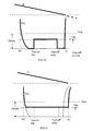
- FIG. 3(A) is the load current-supply voltage characteristics curve
- (B) is the generic structure of the buck regulator.
- FIG. 4(A) is the generic waveform of the voltage regulator in PWM (Pulse Width Mode);
- (B) is the multi-phase voltage regulator to minimize the ripple of power supply;
- (C) is the multi-frequency voltage regulator to minimize the ripple of power supply.
- FIG. 5(A) is generic characteristic curve of the buck regulator as shown in FIG. 3B ;
- (B) is the buck regulator without the proper switch timing;
- (C) is the buck regulator with the proper switch timing.
- FIG. 6(A) is the resisterless Zero Current (IZ) timing control circuit
- (B) is the alternative design of resisterless Zero Current (IZ) timing control circuit
- (C) is the alternative design of resisterless Zero Current (IZ) timing control circuit
- (D) is the alternative design of resisterless Zero Current (IZ) timing control circuit.
- FIG. 7(A) is the Zero Voltage (VZ) crossing timing control circuit
- (B) is the alternative design for the triggering voltage of the Zero Voltage (VZ) crossing timing control circuit.
- FIG. 8(A) is the power management (PMU) system of the prior art
- PMU power management
- (B) is the analogy of the digital level shift to the Low Drop Voltage Regulator (LDVR) architecture as shown in FIG. 8C
- (C) is the analogy of the Low Drop Voltage Regulator (LDVR) to the digital level shift circuit as shown in FIG. 8B
- (D) is the unified approach of the green design of PMUx.
- FIG. 9 is the high-level block diagram of schematics for the unified approach of the green design of PMUx in FIG. 8D .
- FIG. 10 is the recycling energy with switching inductor to switch from gate holding 1 state to gate holding 0 state;
- A is the gate holding state H 1 ;
- B is the switch gate state (SG) of the switching inductor;
- C is the switch capacitor state (SC) of the switching inductor;
- D is the gate holding state H 0 ;
- E is the switching waveform of the switching inductor to switch from gate holding 1 state to gate holding 0 state.
- FIG. 11 is the recycling energy with switching inductor to switch from gate holding 0 state to gate holding 1 state;
- A is the gate holding state H 0 ;
- B is the switch capacitor state (SC) of the switching inductor;
- C is the switch gate state (SG) of the switching inductor;
- D is the gate holding state H 1 ;
- E is the switching waveform of the switching inductor to switch from gate holding 0 state to gate holding 1 state.
- FIG. 12 is the hierarchical waveform of the recycling energy green circuit design for Green Power Management Unit (GPMU).
- GPMU Green Power Management Unit
- FIG. 13(A) is the state transition diagram from H 1 to H 0 ;
- (B) is the state transition diagram from H 0 to H 1 ;
- (C) is the combinatory state transition diagram recycling energy between H 0 and H 1 ;
- (D) is the LDVR and SM synchronous PMU having the combinatory state transition diagram recycling energy between H 0 and H 1 .
- FIGS. 14(A) and (B) are the event driven state diagram for the transition from H 1 to H 0 ;
- (A) is the transition from SG to SC being triggered with the zero voltage VZ event;
- (B) is the transition from SC to H 0 being triggered with the zero current IZ event;
- (C) and (D) are the event driven state diagram for the transition from H 0 to H 1 ;
- (C) is the transition from SC to SG being triggered with the zero voltage VZ event;
- D is the transition from SG to H 1 being triggered with the zero current IZ event.
- FIG. 15 is the recycling mechanism corresponding to the state diagram as shown in FIG. 13C ;
- (A) is the zero voltage-crossing event (VZ);
- (B) is the zero current crossing event (IZ).
- FIG. 16 is table for the Energy Recycling Drive corresponding to FIG. 15 .
- FIG. 17 is the fast transient response power management unit (PMUx) with the low drop voltage regulator (LDVR) triggering switch mode (SM) buck regulator.
- PMUx fast transient response power management unit
- LDVR low drop voltage regulator
- SM switch mode
- FIG. 18 is the hierarchical state diagram for the green PMUx of FIG. 9 .
- FIG. 19(A) is the generic circuit of the power amplifier; (B) is the biasing voltage effects on the power dissipation; (C) is the power supply V DD effects on the power dissipation.
- FIG. 20 is the A type power amplifier PA-A; (A) is the operation of the conventional PA-A; (B) is the operation of the green PA-A; (C) is the circuit of the green PA-A.
- FIG. 21(A) is the operation of the differential B type power amplifier PA-B;
- (B) is the operation of the differential C type power amplifier PA-C;
- (C) is the Doherty amplifier with the differential B type power amplifier PA-B and the differential C type power amplifier PA-C.
- FIG. 22(A) is the operation of the differential B type power amplifier PA-B having the scaling power supply;
- (B) is the operation of the differential C type power amplifier PA-C having the scaling power supply;
- (C) is the Doherty amplifier with the differential B type power amplifier PA-B and the differential C type power amplifier PA-C having the scaling power supply.
- FIG. 23 is the MOS version differential power amplifier;
- A is the complete differential PA having the recycling energy resonator and the feedback latch type switch;
- B is the PA with the recycling LC resonator;
- C is the PA having the N-side feedback switch and the recycling energy resonator;
- D is the differential PA with the recycling energy LC resonator;
- E is the differential PA with the recycle inductor and the cross feedback latch.
- FIG. 24 is the bipolar version differential power amplifier;
- A is the complete differential PA having the recycling energy resonator and the feedback latch type switch;
- B is the PA with the recycling LC resonator;
- C is the PA having the N-side feedback switch and the recycling energy resonator;
- D is the differential PA with the recycling energy LC resonator;
- E is the differential PA with the recycle inductor and the cross feedback latch.
- FIG. 25(A) is the single to differential conversion balun;
- (B) is the MOS version of single to differential conversion and differential PA; it is for both B type power amplifier PA_B and C type power amplifier PA_C;
- (C) is the bipolar version of single to differential conversion and differential PA; it is for both B type power amplifier PA_B and C type power amplifier PA_C.
- FIG. 26(A) is the power scaling voltage generator, the adaptive A type power amplifier PA_A biasing generator and the adaptive C type power amplifier PA_C biasing generator;
- (B) is the adaptive C type power amplifier PA_C biasing;
- (C) is the adaptive C type power amplifier PA_C biasing with power scaling voltage.
- FIG. 27(A) is the on-chip Xtaless clock generator for green chip design; it has the LC tank resonator and frequency-phase lock loop FPLL with ⁇ Average and frequency compensation over temperature with the adjustment of resistance; (B) is the VCO having the frequency compensation over temperature with the adjustment of resistance as shown in FIG. 27A .
- FIG. 28(A) is the LC resonator for the Xtaless clock generator and the FPLL of green chip design as shown in FIG. 27 :
- (B) is the green circuit of the high speed low power latch for the LC resonator for divider of the Xtaless clock generator as shown in FIG. 27 ;
- (C) is the green circuit of the high speed low power FIFO for divider of the LC resonator for the Xtaless clock generator as shown in FIG. 27 ;
- (D) is the low power high speed logic/digital circuit clock waveform of preset and evaluation as shown in FIG.
- (E) is the OR/NOR gate of low power high speed green logic circuit
- (F) is the AND/NAND gate of low power high speed green logic circuit
- (G) is the characteristics curves of the submicron MOS device
- (H) is the low power bandgap voltage reference generator for the green circuit design.
- FIG. 29(A) is the conventional fractional PLL
- (B) is the state transition diagram of the PRNG (Pseudo Random Number Generator)
- (C) is the spur generated by the conventional fractional PLL due to the pseudo-random chaotic pattern of PRNG
- (D) is the disruptive jumping in infinite continuous domains state transition diagram of the TRNG (True Random Number Generator)
- (E) is the spur free spectrum generated by the spurfree fractional PLL
- FIG. 30(A) is the cutting edge PLL having the TRNG (True Random Number Generator) and the ⁇ AVG average analog signal processing to convert the phase impulses noise to the average clock frequency;
- B) is the block diagram of Integer PLL;
- C) is the block diagram to show the ⁇ ADC encoder and decode of ⁇ AVG analog signal process;
- D) is the schematics for the continuous LPF type ⁇ AVG analog average signal processing to convert the phase impulses noise to the average clock frequency instead of injecting into the VCO directly.
- FIG. 31(A) is the green design for the plasma light system; (B) is the pulse width modulation for the green design for the plasma light.
- FIG. 32 is the versatile resonant cavity design for the plasma light;
- A is the dipole type elliptical resonant cavity design for the plasma light;
- B is the single pole type resonant cavity design for the plasma light;
- C is the twin-pad type resonant cavity design;
- D is the twin-pad type concentrically resonant cavity design;
- E the high light efficiency low RF leakage plasma light bulb for the plasma bulb;
- F the white light energy band structure of the plasma bulb.
- FIG. 33(A) is the thermal safety system for the battery of electrical vehicle (EV);
- (B) is the alternative design for the battery of electrical vehicle (EV); the LED has both the light indication and the thermal safety detection function.
- FIG. 34(A) is the light mirror element having a pair of dipole electrodes;
- B) is the light mirror element having a pair of single pole electrodes;
- C) is the operation of the light mirror element having a pair of dipole electrodes;
- D) is the operation of the light mirror element having a pair of single pole electrodes;
- E) is the first step to dope the first pole on the light mirror element;
- F) is the second step to dope the second pole on the light mirror element.
- FIG. 35(A) is the light mirror element; (B) is the matrix of the light mirror elements for digital light processor of the projective TV.
- FIG. 36(A) is the laser light projective system; (B) is the vertical scanning projective light element; (C) is the horizontal scanning projective light element.
- FIG. 37(A) is the constructive process of the digital concave mirror for the lasercom;
- (B) is the Analog Light Processor (ALP) concave mirror implemented with the light mirror element;
- (C) is the alignment of the light mirror elements for the concave mirror;
- (D) is the lasercom system with the ALP concave mirror being made of the light mirror elements
- FIG. 38(A) is the whole schematics of the power management device with the power amplifier device as shown in FIG. 20C ; (B) is the merge of the power management with the power amplifier to be the green circuit design of the power-managing amplifier (PMA).
- PMA power-managing amplifier
- FIG. 39 is the high voltage version of the green circuit design of the power-managing amplifier (PMA).
- FIG. 40(A) is the output waveform of N type switching device power amplifier PA;
- B) is the fundamental mode plus the 1 st and 3 rd harmonics N type class-F power amplifier;
- C is the output waveform of P type switching device power managing amplifier PMA;
- D is the comparison of the plasma light power efficiency of the N-type PA-E and PA-F with the P-type PMA-B, PMA-C, PMA-D, PMA-E, PMA-F.
- FIG. 41(A) is the A, B and C type power managing amplifier PMA; (B) is the different input waveforms; (C) is the delivery output power of PMA power always being 100%; (D) is the comparison of the output power efficiency between the PA and PMA.
- FIG. 42 is adopting the energy flow concept to show the difference between the switch-capacitor-DC-loss N type PA and the switch-capacitor-DC-recycling P type PMA;
- a 1 is the N-switch off and the DC energy stored in LC tank;
- a 2 is the N-switch on and the DC energy dissipation;
- a 3 is the N-switch on and inductor current is built up;
- a 4 is the N-switch off and the inductor current converting to charge;
- B 1 ) is the P-switch off that no DC energy stored in LC tank;
- (B 2 ) is the P-switch on and charging up capacitor to store the DC energy in LC tank;
- B 3 is the building up of inductor current;
- B 4 is the capacitor-stored DC energy converting to the inductor current that the stored DC energy is recycled to be the LC tank oscillatory energy.
- FIG. 43(A) is the N type self-adaptive oscillatory PA;
- B) is the P type self-adaptive oscillatory PA;
- C) is the push-pull N type self-adaptive oscillatory PA;
- D is the push-pull P type self-adaptive oscillatory PA.
- FIG. 44(A) is the waveform of the A type power managing amplifier (PMA) with the option of the adaptive V DD ;
- (B) is the waveform of the A type power managing amplifier (PMA) with the option of the adaptive bias;
- C) is the schematics of the A type power managing amplifier (PMA).
- FIG. 45(A) is the waveform of the B type differential power-managing amplifier (PMA);
- B) is the waveform of the C type differential power-managing amplifier (PMA);
- C is the Doherty power-managing amplifier having both the B type differential power-managing amplifier (PMA) and C type differential power-managing amplifier (PMA).
- FIG. 46 is the Doherty power managing amplifier with the scaling power and adaptive bias; (A) is the waveform of the B type power managing amplifier PMA with the scaling power and adaptive bias; (B) is the waveform of the C type power managing amplifier PMA with the scaling power and adaptive bias; (C) is the Doherty power managing amplifier having both the B type power managing amplifier PMA and C type power managing amplifier PMA with the scaling power and adaptive bias.
- FIG. 47(A) is the differential power managing amplifier having the cross coupling and energy recycling mechanism
- (B) is the simplified differential power managing amplifier having the cross coupling and energy recycling mechanism
- (C) is the simplified differential power managing amplifier having the p-side cross coupling and energy recycling mechanism
- (D) is the simplified differential power managing amplifier having the energy recycling mechanism
- (E) is the simplified differential power managing amplifier having the cross coupling mechanism.
- FIG. 48 is the bipolar version of the differential power managing amplifier PMA;
- A is the differential power managing amplifier having the cross coupling and energy recycling mechanism;
- B is the simplified differential power managing amplifier having the cross coupling and energy recycling mechanism;
- C is the simplified differential power managing amplifier having the p-side cross coupling and energy recycling mechanism;
- D is the simplified differential power managing amplifier having the energy recycling mechanism;
- E is the simplified differential power managing amplifier having the cross coupling mechanism.
- FIG. 49(A) is the MOS version of the single to differential conversion and differential power managing amplifier PMA; (B) is the bipolar version of the single to differential conversion and the differential power-managing amplifier PMA.
- FIG. 50(A) is the biasing voltage generator and the virtual ground power supply, etc for the P-type PMA;
- (B) is the input voltage plan for the constant ground power supply;
- (C) is the input voltage plan with the scaling ground power supply.
- FIG. 51(A) is the N type distributed type microwave power amplifier
- (B) is the home network using the power line and provides the charging for battery
- (C) is P type distributed type microwave power amplifier.
- FIG. 52(A) is the A type, B-type, C type PMA-A, PMA-B and PMA-C;
- (B) is the push-pull A type, B-type, C type PMA-A, PMA-B and PMA-C;
- (C) is the push-pull A type PMA with balun.
- FIG. 53(A) is the D type PMA-D;
- (B) is the push-pull D type PMA;
- (C) is the push-pull A,B,C and D type PMA.
- FIG. 54(A) is the E type PMA; (B) is the F type PMA; (C) is the 3 rd order two stage F type PMA.
- the green technology is to save the earth.
- the green technology includes both the recycling of the resource and saving energy. To save the energy, we need to save the electricity of the power consumption.
- FIG. 1 it is the power flow in the modern society. The power flows from the AC adaptor to Power Management Unit (PMU) then to different electrical devices. The power conversion process is not efficient. The electrical devices power efficiency is not efficient, either. It wastes a lot of power.
- PMU Power Management Unit
- the electrical devices power efficiency is not efficient, either. It wastes a lot of power.
- To have the green technology we develop the unified green circuit technology platform which can apply across the different fields. First, we have to recognize the power efficiency problems in the versatile electrical facilities.
- FIG. 2A shows the clock driven microprocessor, graphics chip, etc having the instantaneous voltage drop of the power supply at the clock edge.
- FIG. 2B shows the modern communication OFDM has the instantaneous amplitude varies causing the power efficiency problem.
- FIG. 2C shows the instantaneous amplitude is transformed to be the adaptive biasing problem of A-type power amplifier (PA-A) problem.
- the dotted line 36 is the adaptive bias voltage for the PA_A.
- FIG. 2D shows the instantaneous amplitude is transformed to be the differential end problem of B-type power amplifier PA-B problem.
- the B+ portion is the waveform for the positive input Vin+ and the B ⁇ portion is the waveform for the positive input Vin ⁇ .
- FIG. 2E shows the power management unit (PMU) charging the electric battery which has both the power efficiency and thermal run-away explosion security problems.
- FIG. 2F shows the temperature monitor for many batteries in the electrical vehicle (EV).
- FIG. 2G shows the plasma light system which the electrical power is converted to the RF (radio frequency) to light the plasma light bulb 34 . The frequency is determined by the resonant cavity. To dimmer the plasma light, as shown in FIG. 2H , the supply power voltage must be able to change for PA type power amplifier.
- the green circuit design includes problems of power efficiency, power linearity, fidelity, dynamic transient response, safety, etc.
- FIG. 3A is the industrial power management unit specification for the microprocessor to address on the power loading I load and power voltage V sup requirements. It relies the on-board capacitor to damp out the ripples in the power line. However, for the power management unit having large capacitor, it doesn't have the fast response for the cellular phone power management unit requirement. For the cellular phone, the power management unit voltage has to vary at least in mega-hertz bandwidth range for crest factor correction for the high Peak to Average Ratio (PAR) signal in the baseband signal modulation. As shown in FIG. 3B , it is the output driver of the power management unit.
- PAR Peak to Average Ratio
- the voltage drop across the PMOS or NMOS is less than 30 mv, i.e., Vds ⁇ 30 mV. Therefore, the output device is large. To switch the large output devices, it takes a lot of energy and it causes the switch loss of the power management unit. Therefore, for the PMU design, we have two losses to consider, the resistive loss and the switch loss.
- FIG. 4A shows the conventional pulse width modulation (PWM) for the power management.
- PWM pulse width modulation
- the switching frequency of PWM is fixed.
- the multi-phase power management unit is adopted by the most power chip manufactures today. It uses multiple drivers in parallel. However, this is not good solution.
- FIG. 4C we can increase the switching frequency to be multi-frequency having the same effect to reduce the voltage ripple of power supply. Comparing the number of the switch period of the multi-phase PMU with the number of the switch period of the multi-phase PMU, the switching times are the same. In other words, the switching loss of the multi-frequency PMU is the same as the multi-phase PMU.
- the multi-phase PMU uses more components, the switching loss is still the same. Therefore, the multi-frequency PMU is much better solution than the multi-phase PMU solution. Furthermore, even the switching loss is proportional to the switching times, with the green technology of switch inductor, the switching loss is not proportional to the switching times. With the switch inductor green technology, the switching energy recycles in the switching circuit. Therefore, the multi-frequency PMU does not have the switching loss problem. As the switching frequency increases, the component sizes of PMU can be reduced a lot. However, the multi-phase PMU doesn't have this benefit at all. The frequency is still kept the same, the sizes of the components are still kept the same. Since the multi-phase PMU has multiple drivers, it is very difficult for each driver to have the individual switch inductor driving circuit. Therefore, all the power chip industry has run in the wrong direction of the multi-phase switch mode voltage regulator.
- the fast transient of PMU voltage shift problems has two phases.
- One phase is for the wireless application.
- the PMU voltage is needed to shift from one voltage level to another voltage level.
- the other phase is for the microprocessor application which has the power surges. Therefore, the PMU needs to have much complex dynamic design.
- the event-driven state transition diagram is needed to develop for the green technology.
- the charging device PMOS
- the inductor current I L and the power supply voltage V sup increase.
- the PMU charging device is switched off and the output voltage Vo and inductor current I L decrease.
- the output voltage Vo is equal to the ground voltage, it is the zero-voltage crossing (ZV) and the discharging device (NMOS) can be turned on without the worry of the crowbar current of shorting V battery to Ground.
- the discharging device (NMOS) is turned on, the inductor current I L flows through the discharging device (NMOS) to pump the charges from the ground.
- FIG. 5B shows the discharging device (NMOS) turns on late and turn-off early cases.
- FIG. 5C shows the perfect timing at the VZ and IZ events. There are no voltage dips from the ( ⁇ V ds ) voltage to ( ⁇ V diode ) voltage.
- FIG. 6 is the schematic of the resistorless IZ detector. There are versatile forms of IZ detector. As shown in FIG. 6A , the measured voltage V I is
- V I is
- the measured voltage V I is
- the measured voltage V I is
- the comparator triggers the IZ signal to notify the zero crossing.
- FIG. 7 is the cross-zero voltage VZ detector.
- the most difficult problem for the VZ detector is the driver circuit switch circuit delay.
- the discharging device NMOS
- To determine the voltage V switch is an adaptive process.
- the discharging device (NMOS) switch-on time is compared with the Vo zero-crossing time. If the time is earlier, decreases the switching voltage V switch to trigger the switch later. If the time is late, increase the voltage V switch to trigger the switch earlier.
- This mechanism can be performed with the Phase detector (PD), Charge Pump (CHP) and Low Pass Filter (LPF).
- PD Phase detector
- CHP Charge Pump
- LPF Low Pass Filter
- FIG. 7B the same function can be implemented with the alternative design of Phase detector (PD), Increment/Decrement Counter and digital to analog converter (DAC).
- VZ detector had better to implemented with the low power high-speed circuit as shown in FIG. 28E and FIG. 28F .
- the Low Drop Voltage Regulator (LDVR) and the Switch Mode Buck Regulator (SM) are two independent circuits.
- the Low Drop Voltage Regulator (LDVR) is equivalent to the analog level shift circuit.
- the LDVR is only working in the pull up voltage supplying mode. It is no use to have the pull down mode. It is the single side operation. Therefore, today's LDVR has the 3 rd stage analog buffer is omitted.
- the 2 nd stage level shift serves as the analog buffer, too.
- This omission of the 3 rd stage of amplifier causes the stability-induced problems such as rushing-in current, over-voltage, etc. Therefore, today LDVR has the serious analog architecture and circuit configuration problems.
- the industry just follows the same mistake. Until now, there is nobody want to correct this fundamental mistake.
- the fundamental problem is that there is no correct analog buffer design except the unit gain buffer.
- the digital level shift circuit has three stages.
- the analog level shift circuit of LDVR should have the analog buffer to be three stages analog architecture and circuit configuration.
- the analog level shift circuit of LDVR in FIG. 8C and the switch Mode Buck Regulator (SM) in FIG. 8A we can have the unified PMUx architecture as shown in FIG. 8D which is corresponding to FIG. 3A .
- the unified PMUx architecture can have the fast transient, minimum error and power efficiency. As shown in FIG. 9 , it shows the detailed architecture of the unified PMUx.
- FIG. 9 there are the Switch Inductor Recycling Driver ( FIG. 15 ), LDVR Controller ( FIG. 17 ), VZ Adaptive Zero-Crossing Detector ( FIG. 7 ), IZ Zero-Current Detector ( FIG. 6 ), Switch Mode Power Control and Unified PMU Control ( FIG. 18 ) including SM & LDVR Re-synchronizer.
- the Switch Inductor Recycling Driver is the key technology of the green circuit design to minimize the switch loss of PMU. For high frequency operation of the PMUx, the switching energy of the output driver is recycling that the PMUx switch loss will not increase as switching frequency increases.
- a green means to deliver energy comprises an energy cycling mechanism.
- the energy cycling mechanism recycles the residual energy in the green energy means. Instead of discharging the residual energy, the energy cycling mechanism moves the residual energy to other portion of the green energy means.
- the switch inductor is the combination of two switches SC, SG and one inductor. As shown in FIG. 10 , there are four states, H 1 , H 0 , SG and SC.
- H 1 means the gate voltage is in the hold state 1 .
- the pull up P device is on to hold the gate at 1 state.
- H 0 means the gate voltage is in the hold state 0 .
- the pull down N device is on to hold the gate at 0 state.
- the SG state means the gate SG is turned on.
- the SC state means the gate SC is turned on.
- the gate In the H 1 state, the gate is held in 1 state. The positive charge is stored in the parametric gate capacitor. C gate . The pull up P device is on.
- the pull up P device is off.
- the switch SG is connected to the ground to build up the inductor current to store the energy in the inductor current.
- the double threaded arrow represents the flow direction of the current.
- the switch SC switches on to transfer the charge to the capacitor C stor .
- the switch SC turns off to finish the transfer of energy from capacitor C gate to capacitor C stor completely.
- the pull down N device turns on to hold the state at 0 state.
- FIG. 10E shows the waveform of the switches SC, SG, P — and N in the four states of H 1 , SG, SC and H 0 .
- FIG. 11 shows the recycling switch driver switches from the 0 state to 1 state.
- H 0 state the pull down device is on to hold the gate voltage at 0 state.
- SC state the pull down device N is turned off and the switch SC is turned on.
- the inductor current flows from the capacitor C stor to the gate C gate .
- the state is transferred from SC state to be the SG state.
- the switch SC is turned off and the gate SG is turned on.
- the current flows from the ground to the C gate .
- As the inductor current I L is zero, the state is transferred from the SG state to the H 1 state.
- the switch SC is off and the pull up device P is on to hold the gate C gate at 1 state.
- FIG. 12 it shows the global view of the timing relation between the switch mode buck regulator and the switch inductor.
- the P drive MP is the P device of the buck regulator; the MP — is the waveform of the inverse signal of the gate signal MP.
- the N drive MN is the N device of the buck regulator; the MN is the waveform of the gate signal MN.
- the duty cycle is DT.
- the switch delay can be compensated with the preset time to trigger the switch action earlier. Just as the case of VZ to have the delay loop compensation for the switch delay, all the other events can be compensated the switch delay with the same way.
- the P drive switch repeats with the pattern of H 0 ,SC,SG,H 1 ,SF,SC,H 0 ; the N drive switch also repeats with the pattern of H 0 ,SC,SG,H 1 ,SF,SC,H 0 .
- FIG. 13A it is the transition from H 1 to H 0 state diagram.
- FIG. 13B it is the transition from H 0 to H 1 state diagram.
- FIG. 13C we combine the FIG. 13A with FIG. 13B , the transitions is recycling in the state diagram.
- FIG. 9 and FIG. 17 we can add the extra LDVR driven switching activations in the state diagram, too.
- the transition among the switch inductor switch state diagram is event-driven.
- the transition from SG to SC is the Zero-Voltage Crossing VZ event.
- C gate voltage is zero, turn off the SG and turn on SC.
- the transition from SC to H 0 is the Zero-Current Crossing IZ event.
- the inductor current is zero, turn off the switch SC then turn on N device to hold Cgate at H 0 state.
- the transition from SC to SG is the Zero-Voltage Crossing VZ event.
- C stor voltage is zero, turn off the SC and turn on SG.
- the transition from SG to H 1 is the Zero-Current Crossing IZ event.
- the inductor current is zero, turn off the switch SG then turn on P device to hold Cgate at H 1 state.
- the state transition between SC and SG can share with one VZ detector circuit.
- the transition from SC to H 0 and the transition from SG to H 1 can share one IZ detect circuit.
- the multiplex we can configure the IZ detector and VZ for different event driven state diagram transition.
- the logic table for the event driven switch inductor drive is summarized in the Table of Energy Recycling Drive.
- the SM is power efficient but slow transient response.
- the analog buffer of the LDVRx as shown in FIG. 17 is low power and has fast transient response. Therefore, the PMUx of the hybrid LDVRx-SMx has both the power efficient and fast transient response. Furthermore, the fast LDVR transient current will convert to be the SM switching current that the energy is recycling and the LDVRx still has the SMx power efficiency.
- FIG. 18 is the global view of the hierarchical state transition diagram of the green PMU circuit design. Even the state diagram looks so complex, it is noted that a lot of state transition is embedded in the architecture and system itself. So, the implementation has been simplified a lot. As shown in FIG. 3A , FIG. 9 , FIG. 12 and FIG.
- the LDVR upper triggering voltage VUCN (upper N device clamping voltage) is larger than VU.
- the LDVR lower triggering voltage VLCP (lower P device clamping voltage) is less than VL.
- the SM & LDVR Re-synchronizer in FIG. 9 is only to keep the relation of VUCN>VU>VL>VLCP. So the synchronization of LDVR and SM is embedded in the architecture and system design.
- FIG. 19A is the generic power amplifier of all the power amplifier design today.
- the input Vin is AC coupled with the input N device.
- the load for the power amplifier is the inductor L. Adjusting the bias of input Vin, the power amplifier works as A, B and C different modes.
- FIG. 19B shows the Vin with different bias conditions.
- V TN is the threshold voltage of the N device. It is the V GS for the NMOS device and V BE for the bipolar device.
- V in V bias +A sin( ⁇ t )
- the V DC induces the I DC .
- the conventional PA-B power amplifier only has half period of modulation. For the unsymmetrical OFDM modulation signal, etc, it will lose the signal information and lose the fidelity of the signal. Therefore, we need to have the differential B type power amplifier DPA-B for the OFDM signal.
- the differential has two-fold effects of (1) fidelity to have the high linearity effect; (2) power recycling to have high power efficiency effect
- the V KN is the kink voltage which is the minimum of the output voltage for N type device.
- the kink voltage V KN is the V DS for the NMOS device and V CE of the bipolar device.
- the DC area below the line V DD is the waste energy. To reduce the waste of the power, we can adaptive adjust the power according to the Vin input waveform to reduce the voltage of the power supply V DD .
- FIG. 20 it is the adaptive power and bias A type power amplifier APB-A-PA.
- the input Vin has the unnecessary waste of energy due to the DC bias V bias .
- FIG. 20B we can reduce the voltage level of the bias V bias to reduce the DC waste.
- the Vout waveform must be higher than the kink voltage V KN .
- the amplitude of V out is small, as shown in FIG. 20B , we can reduce the voltage level of the power supply V DD to reduce the DC power waste.
- Both the V DD and V bias can be scaled and adjusted according to the amplitude of the input signal Vin. As shown in FIG.
- the amplitude detector detects the amplitude of the input signal V in .
- the amplitude detect sends the amplitude information to the Power Supply Generator to generate the adaptive scaling power V DD .
- the adaptive scaling power V DD is send to the Bias Generator to generate the adaptive bias for the power amplifier.
- the Bias Generator can be as simple as a Voltage Divider.
- a delay circuit can be inserted in the signal path of Vin.
- PD Peak Synchronizer Phase Detector
- Delay Controller to adjust the delay to match the V in with the adaptive bias and adaptive power.
- FIG. 21 shows the differential B type and C-type power amplifier DPA-B, DPA-C to work as the high linearity Doherty Amplifier.
- the differential power amplifier DPA-B input V in — B+ and V in — B ⁇ are biased at the threshold voltage level VTN.
- the differential power amplifier DPA-C input V in — B+ and V in — B ⁇ are biased below the threshold voltage level V TN .
- FIG. 21C is the schematics for the differential Doherty Power amplifier.
- the single end signal V in is converted to be the differential signal V in — B+ and V in — B ⁇ with the B Signal Generator.
- the single end signal V in is converted to be the differential signal V in — C+ and V in — C ⁇ with the C Signal Generator.
- the differential power amplifiers DPA-B and DPA-C generate the differential RF outputs and merge them together.
- the scaling power supply and adaptive bias techniques are adopted.
- the differential B type and C-type power amplifier DPA-B, DPA-C to work as the high linearity Doherty Amplifier with the scaling power supply and adaptive bias techniques.
- the differential power amplifier DPA-B input V in — B+ and V in — B ⁇ are biased at the threshold voltage level V TN .
- the output voltage V o — B+ and V o — B ⁇ oscillate with the scaling power supply level V DD being the centerline.
- FIG. 22 the differential power amplifier DPA-B input V in — B+ and V in — B ⁇ are biased at the threshold voltage level V TN .
- the output voltage V o — B+ and V o — B ⁇ oscillate with the scaling power supply level V DD being the centerline.
- FIG. 22B is the schematics for the differential Doherty Power amplifier with the scaling power supply and adaptive bias.
- the amplitude detector detects the amplitude of the input signal Vin and generates the amplitude of Vin.
- the Vin amplitude information is sent to the Power Supply Generator to generate the scaling power supply V DD for the power amplifier.
- the Vin amplitude information is also sent to the Adaptive Bias_C Generator to generate the adaptive bias voltage for the power amplifier DPA-C.
- the single end signal Vin is converted to be the differential signal V in — B+ and V in — B ⁇ with the B Signal Generator.
- the single end signal V in is converted to be the differential signal V in — C+ and V in — C ⁇ with the C Signal Generator.
- the differential power amplifiers DPA-B and DPA-C generates the differential RF outputs and merge them together.
- the differential power amplifier DPA is as shown in FIG. 23 . With the different bias conditions, the differential power amplifier DPA can operates as A type DPA-A, B type DPA-B and C type DPA-C.
- the input is a pair of NMOS device.
- V in+ and V in ⁇ are the inputs; V o+ and V o ⁇ are the outputs.
- FIG. 23A is the complete set of the DPA which has the inductor load, cross-coupling PMOS, cross-coupling NMOS, the energy recycling LC tank.
- FIG. 23B is the DPA which has the cross-coupling PMOS, cross-coupling NMOS, the energy recycling LC tank.
- the LC tank has the dual function of energy recycling and inductor load.
- FIG. 23C is the DPA which has the inductor load, cross-coupling NMOS, the energy recycling LC tank.
- FIG. 23D is the DPA which has the inductor load, and the energy recycling LC tank.
- FIG. 23E is the DPA which has the inductor load, cross-coupling NMOS and the energy coupling inductor.
- the Bipolar differential power amplifier DPA is as shown in FIG. 24 .
- the differential power amplifier DPA can operates as A type DPA-A, B type DPA-B and C type DPA-C.
- the input is a pair of NPN device.
- V in+ and V in ⁇ are the inputs;
- V o+ and V o ⁇ are the outputs.
- FIG. 24A is the complete set of the DPA which has the inductor load, cross-coupling PNP, cross-coupling NPN, the energy recycling LC tank.
- FIG. 24B is the DPA which has the cross-coupling PNP, cross-coupling NPN, the energy recycling LC tank.
- the LC tank has the dual function of energy recycling and inductor load.
- FIG. 24C is the DPA which has the inductor load, cross-coupling NPN, the energy recycling LC tank.
- FIG. 24D is the DPA which has the inductor load, and the energy recycling LC tank.
- FIG. 24E is the DPA which has the inductor load, cross-coupling NPN and the energy coupling inductor.
- FIG. 25A it is the balun to convert the single end to differential ends.
- the single end signal is convert to the differential end signals with the differential amplifier which is biased at the A-type biasing voltage V Bias — A .
- the 2 nd stage is the differential power amplifier DPA.
- FIG. 25C is Bipolar version of the S2D and DPA.
- the Doherty power amplifier uses a lot of scaling power generator and bias generator.
- FIG. 26A there are the Amplitude Detector, Bias_A Generator, Bias_B Generator, Bias_B Generator, Adaptive Bias_C and Generator Power Supply Generator.
- FIG. 26B it is the plan for the input Vi of the Differential Doherty power amplifier as shown in FIG. 21 .
- FIG. 26C it is the plan for the input Vi of the scaling power and adaptive bias voltage Differential Doherty power amplifier as shown in FIG. 21 .
- the Xtaless Clock Generator and Spurfree FPLL are the important green circuit designs. Crystal clock consumes a lot of energy that it has to be replaced with the Xtaless Clock Generator. As shown in FIG. 27 . the green circuit design of Xtaless Clock Generator and Spurfree FPLL can be implemented on-chip to save both resource and energy.
- the on-chip low Q inductor to build the high Q LC resonator.
- the capacitors C lam and C onj are to clamp the v com and g com to be constant voltage to reduce the oscillation self-induced switching noise.
- adjust the capacitor C 8 series resistance R C 8R to be equal to the parametric resistance R L of the inductor L, the oscillation frequency of the LC tank 1 will be independent of the temperature. So, the clock frequency reference LC tank is compensated with the capacitor resistance 8R and the frequency variation is adjusted with FPLL, the Xtaless Clock Generator has both temperature and frequency high performance.
- FIG. 28B is the high-speed latch (HSL) of green flip-flop GFF.
- a green means comprises a fast latch.
- the fast latch comprises a pair of cross-coupling p type device and a pair of n type device being activated by one clock.
- a pair of cross-coupling n type device being activated with the reverse phase of the clock.
- GFF green flip-flop
- HSL high-speed latch
- a green means comprising a fast flip-flop
- the flip-flop comprises a pair of latches.
- a pair of output terminals of the first latch are connected to a pair of inputs of the second latch.
- the clock of the first latch and the clock of the second latch are in reverse phase.
- FIG. 28D show the green logic circuit design.
- the clock generator generates the non-overlapping clock. At the falling of the non-overlapping clock, the preset signals are generated to preset the NOR/OR gates in FIG. 28E and the NAND/AND gates in FIG. 28F .
- a green means has high-speed low power logic
- a clock generator means generating non-overlapping clocks and pre-setting signal.
- the pre-setting signal is in an interval between said non-overlapping clocks.
- the pre-setting signal presets the logic gates in pre-setting states and evaluates in an interval of the non-overlapping clocks.
- FIG. 28G shows the characteristics curve of the submicron logic circuit speed with the frequency of VCO of ring oscillator. As the temperature increases, both the threshold voltage V th and the mobility ⁇ decrease. As the VDD is small, Vth dominates the speed of logic circuit. As VDD is high, mobility ⁇ dominates the speed of logic circuit. As shown in FIG. 28G , there is a cross point on the f —vco vs V DD curve.
- the conventional Phase Lock Loop PLL has many fundamental conceptual mistakes.
- the PLL has a lot of jitter and spur which cannot eliminate due the wrong design concepts.
- FIG. 30A it is the correct green circuit design of the FPLL. Comparing the FPLL with conventional PLL, it shows the fundamental mistakes in the conventional Phase Lock Loop PLL design.
- the LC VCO LCO
- the LC VCO is the resonator has the 2 nd order filter effect. It is a noise filter. In the phase based small phase signal model never consider the LCO filter effect.
- the PFD generates UP and DOWN is the ⁇ converter type noise signal.
- the conventional factorial Phase Lock Loop PLL has the ⁇ ADC.
- the conventional factorial Phase Lock Loop PLL still uses the phase detector PD, charge pump CHP and Low Pass Filter LPF.
- the conventional factorial Phase Lock Loop PLL has the ⁇ ADC, but it doesn't have the analog average signal process ⁇ AVG.
- the fundamental principles of communication theory there should be the symmetry in the encoder and decoder path as shown in FIG. 30C .
- the conventional factorial Phase Lock Loop PLL has only ⁇ ADC. It does not have the analog average signal process ⁇ AVG. In other words, the conventional factorial Phase Lock Loop PLL completely violates the fundamental principle of the communication theory.
- the conventional factorial Phase Lock Loop PLL uses the Pseudo-Random Number Generator (PRNG).
- PRNG Pseudo-Random Number Generator
- PRNG Pseudo Random Number Generator
- FIG. 29B the PRNG generates the chaos cannot use as the Random Number Generator (RNG).
- RNG Random Number Generator
- the state in PRNG is step one by one.
- the randomness distance between two successive states is only one. Therefore, the chaos has very similar repetitive pattern.
- the repetitive pattern will generate the spur in the spectrum as shown in FIG. 29C .
- the green circuit FPLL uses the on-chip CMOS compatible True Random Number Generator (TRNG).
- the TRNG is generated with randomized chaos, not chaos only. In other words, the chaos has been further processed with the randomized process to be randomized chaos.
- the state of TRNG is infinite in analog voltage and continuous time domains. Furthermore, the state is jumping in the state domain. The randomness distance between two states is far away. The pattern never repeats itself that it is spurfree as shown in FIG. 29E .
- the green design of frequency and phase lock loop FPLL adopts the analog average signal process ⁇ AVG and TRNG that it is jitterless in time domain and spurfree in frequency domain.
- the analog average signal process ⁇ AVG is shown in FIG. 30D .
- the analog average signal process ⁇ AVG is implemented with the continuous in time analog circuit.
- the Xtaless clock generator is very important in the green circuit design for the electronic power plasma lighting industry, too.
- the resonator cavity has specified wavelength. It is corresponding to the switch signal has the specified frequency which is derived from the Xtaless clock generator.
- the power management unit PMUx
- the power amplifier delivers the resonate power to the antenna in the RF resonator.
- the power amplifier is the resonator in time domain; RF resonator is the resonator in space domain.
- the wavelength in space domain determines the frequency in time domain. To generate the frequency correctly for the electronic plasma light, it needs the Xtaless clock generator.
- the oscillation amplitude is operated at the full range of the power supply.
- To have the oscillation amplitude is full range of the power supply, it is to adjust the pulse width of power amplifier.
- the lighting material energy band gap structure will determine the frequency of the oscillation in the RF resonator.
- the dielectric material in the RF resonator and the frequency of the oscillation determines the size the RF resonator.
- the frequency of the oscillation determines the switch frequency of the input-switching signal of the power amplifier.
- To control the light intensity use the voltage level of the power supply. To get the most efficiency, use the pulse width of the switching signal.
- the maximum peak detector and the minimum detector to detect the output RF power of the power amplifier. If the amplitude is less than the full range, increase the pulse of modulation. To detect the RF power is full range or not, it is to compare the upper half of the amplitude and the lower half of the amplitude. If the upper half of the amplitude is larger than the lower half of the amplitude, the lower half of the amplitude is truncated with the kink voltage V KN . It is to reduce the pulse width. If the upper half of the amplitude is less than the lower half of the amplitude, the amplitude is less than the full span. It is to increase the pulse width. If the minimum peak voltage is larger than the kink voltage, it is not full span and increases the pulse width directly.
- FIG. 32 shows the different design of the RF resonator.
- the resonator uses the high dielectric material to fill in the cavity. There is coating of RF reflective material on the surface or using the cassette cavity to reflect the RF wave to confine the RF wave in the cavity to save the RF energy.
- the cavity is in the elliptic shape that wave emitting from the antenna at the source focus point to the plasma light bulb at the sink focus point of the elliptical resonant cavity. This is two-way resonant.
- the RF energy is sent from the power amplifier to cavity.
- the RF energy in the resonant cavity also reflects from the cavity to the power amplifier. Therefore, the Q of the two-way resonance is much higher and the efficiency to convert the RF energy to be the molecular/atom energy band is much higher. Therefore, the light efficiency is much higher.
- the antenna can be dipole antenna as shown in FIG. 32A . In FIG. 32B , it shows the single pole antenna. In FIG. 32C , it shows the di-pad antenna. In FIG. 32D , it shows the di-pad antenna in the concentric resonant cavity. FIG. 32E shows the bulb of the plasma light. It has the enlarged end to have the radiated plasma to stay outside the oscillation tube. The thin rod is inside the oscillatory cavity. The wave inside the oscillatory cavity is plane wave.
- FIG. 32F shows the energy band structure of the plasma light bulb.
- the RF energy ionizes the gas molecules create gas plasma.
- the gas plasma vaporizes the mercury and halide salts.
- the mercury generates the distinguished energy bands.
- the halide salts smashes the distinguished energy bands to be the continuous spectrum of the white light.
- FIG. 33A shows one design for the battery safety.
- the clock generator continues increasing the counter to be the address to be scan.
- the decoder decodes the address 41 to select the switch in the 1:n multiplex 43 to turn on.
- the current I injects into the bipolar device 38 to measure the temperature in the individual battery. If the temperature is too high and trigger the detect and alarm signal, the detect signal stop the clock and the alarm signal 42 changes the switch to light LED 39 with the 1:2 multiplex 45 to indicate the fault battery.
- a green energy means comprises a temperature sensitive LED 47 , As the current flowing said temperature sensitive LED 47 , the voltage crossing the temperature sensitive LED 47 is varied. As shown in FIG. 33B , it is the simplified design.
- the thermal detect and LED shared the same device. There is the one-hot cycling ring type FIFO 46 . Only one signal is in 1 state in the ring type FIFO chain and the rest is 0 state. The current I an inject the bipolar thermal LED.
- the bipolar thermal LED 47 has the dual function of light and temperature detection. If the temperature is larger than the specified safety margin, the detect signal is triggered and stop the clock of the one-hot cycling FIFO chain 46 and stop the charging operation of PMU.
- the bipolar thermal LED 47 has the steady light to indicate the fault battery.
- the projective TV and lasercom is the lighting processing technology consuming a lot of power.
- the lighting processing technology needs the green design.
- First, to toggle the light micro-mirror is the high voltage operation. The charging and discharging of the light micro-mirror consumes a lot of power.
- a green energy means comprises a light micro-mirror 55 and electric pole.
- the light micro-mirror is doped with electric charge in isolated region 52 to keep storage of the electric charges.
- the electric pole 53 is driven with electricity, the light micro-mirror is rotated to change angle.
- the charges are doped in the isolation layers 52 .
- FIG. 34A the charges are doped in the isolation layers 52 .
- FIG. 34C shows the alternative design of the light micro-mirror. Both the isolation layers are doped with the same electricity. As shown in FIG. 34D , injecting these two poles 53 with different polarity of charges to rotate the light micro-mirror. As shown in FIG. 34E and FIG. 34F , for the bonding wafer technology, the light micro-mirrors can be doped with the electricity in the isolation layer first. The mask 51 will protect the other portion which is not needed to be doped.
- the mask is not needed at all.
- the light micro-mirror wafer 55 is bonded with the circuit wafer 54 .
- FIG. 35A it is the top view of one light micro-mirror element 55 t of the projective TV.
- FIG. 35B it is the light micro-mirror 55 t array for the digital light processing of projective TV.
- the switch inductor technology as shown in FIG. 10 and FIG. 11 can be applied to the digital light processing of projective TV to save the power a lot. There are two ways to implement the switch inductor. The first type is to use the extra capacitor as the store capacitor. The second type is to use the light micro-mirror capacitors as the two capacitors to be the recycling energy capacitors.
- FIG. 1 and FIG. 36 it is the green design for the LaserTV with the light micro-mirror.
- the modulated laser light shines on the vertical scanning mirror 55 v first.
- the horizontal scanning light micro-mirror 55 h array sweeps in the horizontal direction.
- the light is projected on the screen, it is the projective TV.
- FIG. 1 and FIG. 37 it is the LaserCom with the adaptive light micro-mirrors technology.
- the air turbulence causes the defocus dynamically. It induces the blinking in the light transmission.
- the electrical programmable concave micro-mirror 56 and auto light gain control are developed.
- the concave light focus the parallel laser light on the photo sensor locating at the focus point.
- the inclined tiny light micro-mirror 55 c at the plan also can reflect the parallel light to the focus point.
- This is the principle of the light micro-mirror can serve as the programmable concave mirror 56 .
- FIG. 37C it is the top view of the circular programmable concave mirror 56 .
- the micro-mirror can tilt to reflect the light on the focus point.
- FIG. 37D shows the block diagram of the LaserCom. The laser light passes through the telescope lens and the optical attenuator to shine on the Analog Light Processor of Programmable Concave Mirror Light micro-Mirrors.
- the analog light processor 56 adjusts the light micro-mirror angle according to the wave front detector information to reflect the laser light on the focus. Using the splitter, portion of the light shines on the photo-sensor at the focus point. The photo sensor converts the light intensity to the voltage waveform. The peak detector detects the peak value of the light intensity then send it to the automatic gain control AGC circuit. The automatic gain control AGC set the taps of the Optical Attenuator to change the attenuating factor to keep the light intensity to be constant.
- the power management unit PMU output driver and the power amplifier PA are drawn together. There are two inductors. There is the power loss in the power management unit PMU and there is power loss in the power amplifier PA, too. To save the energy, instead of two stages of power loss, we merge these to stages to be one stage of the power management amplifier PMA. As shown in FIG. 38B , the PMU output buffer is merged with PA to be the power-managing amplifier PMA. Now, a breakthrough new power amplifier PMA is invented. Even the PMA is derived from the PMU and PA, it has the completely different characteristics from the PMU and PA. The superior power amplifier PMA has power efficiency more than 95% as the PMU does. However, it behaves like the amplifier, not PMU.
- the high voltage circuit of PMU technologies can be applied to PMA directly.
- the circuit can be divided to be two portions, the high voltage HV and the low voltage LV.
- the modulation signal circuit can be raised up to operate in the high voltage zone.
- the A type power amplifier PA-A has the power efficiency can be 50%; the B type power amplifier PA-B has the power efficiency can be 78%.
- the highest power efficiency is never more than 39%.
- Nobody skeptical the theory and analytical methodology are completely wrong. All the RF design research follows the same wrong track and is trapped in the same trap. We have the multi-disciplinary of both PMU and PA. To our intuition, there is no reason for the PMU can have the 96% efficiency and the PA has the 30% efficiency. It must have something wrong.
- FIG. 40 The analytical methodology is shown as FIG. 40 .
- V out of the conventional PA As shown in FIG. 19A , it is the output voltage V out of the conventional PA. It is the essential characteristic and generic curve of conventional PA to have the inductor connecting the V DD . The power delivery is the sinusoidal curve. There are DC energy at V DD level. Therefore, the maximum efficiency for the V out curve is
- FIG. 40B is the output waveform of the F type PA.
- the output efficiency is the 1 st and 3 rd order waveform shaping to make the output waveform more close to the rectangle waveform.
- FIG. 40C is the essential characteristic and generic curve of conventional PMA to have the inductor connecting the ground as shown in FIG. 38B .
- the power amplifier problem is the circuit configuration problem. All the power amplifier design has used the wrong circuit configuration that they have to struggle with the power efficiency problem.
- the problem originally came from the RF circuit design doesn't know how to design the circuit in the high voltage zone. If they use the N device connected to the ground, they can walk around the circuit problem in the high voltage zone. The new comer in the RF field just follows the old design way. Nobody dares to challenge the old PA design. However, the power efficiency is the nightmare problem for the PA.
- FIG. 41 is the generic circuit and characteristic curves of the PMA.
- the maximum efficiency is less than 33%. It doesn't matter the PA is A,B,C, etc type. It comes from the generic architecture of the inductor being connected to VDD.
- V DC biasing voltage
- the V DC loss is a lot.
- the net power efficiency is only 10%.
- the 10% PA efficiency is coming from the field data of the base station. It causes the base station cannot put the PA on the antenna and it needs a lot of cooling facility and power facility. Considering all the added on overhead factors, the total PA power efficiency becomes only 3%.
- the PMA has the net efficiency more than 90%.
- the PMA can be installed on the antenna directly. It gets rid of the transmission line loss, the power consumption of cooling facility and power facility. It will save one nuclear power plant for the Germany and several nuclear power plants for US. Therefore, it can see how important the power-managing amplifier PMA is.
- the PA and PMA have the conjugated V DD -Gnd symmetrical waveform.
- the PMA has output efficiency to be 100% and PA has output efficiency to be less than 33% and 50%.
- FIG. 42 the detailed analysis shows the PA is switch-cap DC energy dissipation and PMA is switch-cap DC energy recycling. It is proved that the analysis of the output power efficiency is valid and the output power efficiency is a good index for the power efficiency of the architecture design of the power amplifier. Here we use the approximation to show the key issues.
- the capacitors are charged to store the DC energy in the still LC tank.
- the N switch is turned on, the large N device has small resistance that it drains the charges and stored energy in the still LC tank immediately.
- the inductor current starts to drain to store the energy in the inductor.
- the N switch is turned off and the inductor current is converted to the charge stored in the LC tank. The dissipated energy lost is in FIG. 42 A 2 is never recovered.
- the energy stored in the LC tank is zero.
- the P switch is turned.
- the inductor current starts to build up to store the energy in the LC tank.
- the switch is turned off and the stored charge in the capacitor is discharged to be the inductor current.
- the stored energy is recycled to be the LC tank energy.
- the stored DC energy in capacitor is not wasted at all.
- the PA is switch-cap DC-energy dissipation and the PMA is switch-cap DC-energy recycled. That is the reason why PMA has output 100% and PA has output efficiency only 33% or 50%.
- the output efficiency is a good index for the power efficiency of the power amplifier architecture.
- the PMA power amplifier has the very important applications in cellular phone and plasma light.
- the conventional light bulb has only 10% power efficiency to convert the electricity to light. So far, the plasma has power efficiency to be 70%.
- the plasma can be dimmed to be 1% light intensity.
- due to the power efficiency is low at low light intensity, the plasma cannot be used as the home light as shown in FIG. 40D .
- the low efficiency of plasma light at low light intensity is due to the power amplifier. Therefore, to use the high power efficiency to enhance the plasma light efficiency is the most important green design.
- the valley detector detects the valley voltage of the Vo or the plasma resonator amplitude. The valley value is compared with the adjusted reference voltage V adj for dimmer. If the valley voltage is larger than the V adj , the power amplifier starts to pump the RF energy to the plasma light resonator.
- FIG. 43B it is the PMA type optimum adaptive power amplifier system.
- the peak detector detects the peak voltage of the Vo or the plasma resonator amplitude. The peak value is compared with the adjusted reference voltage V adj for dimmer. If the peak voltage is smaller than the V adj , the power amplifier starts to pump the RF energy to the plasma light resonator.
- the IZ current detector is to detect the current flow in the inductor to determine the timing to charge the energy into the LC tank synchronously. As the inductor current is in the same flowing direction as switching current, it is time to open the switch.
- the light resonator has the specific dimension to have the specific wavelength that the power amplifier has the specific switch frequency.
- the specific switch frequency is set as the clock generator ClkGen.
- the driver can be the switch inductor drive or the power amplifier pre-drive. As shown in FIG. 43C , it is the differential push-pull PA type optimum adaptive power amplifier system. As shown in FIG. 43D , it is the differential push-pull PMA type optimum adaptive power amplifier system.
- the differential push-pull PMA type optimum adaptive power amplifier system has the best power efficiency and light efficiency.
- the differential push-pull PMA type optimum adaptive power amplifier will have the global efficiency of 95%. We can use the plasma light to be the home plasma light to replace the light bulb. Comparing with the convention light bulb has only 10%, the PMA is the most important revolution in the green industry.
- FIG. 44 is the A-type power-managing amplifier PMA.
- the biasing voltage is constant, there is more DC power loss.
- the adaptive biasing voltage is shifted according to the amplitude of the envelope. It can reduce the DC power dissipation to increase the efficiency.
- the amplitude detector detects the amplitude of the input signal and makes the adaptive adjustment of the biasing voltage.
- the power efficiency there is no need for the scaling power for the power-managing amplifier PMA anymore unless for the crest factor for the high PAR.
- FIG. 45 shows the B-type differential PMA, C-type differential PMA and the differential Doherty PMA made of the B-type differential PMA and C-type differential PMA. As shown in FIG. 45A , it is the waveform of the B-type differential PMA. As shown in FIG. 45B , it is the waveform of the C-type differential PMA. FIG. 45C is the Doherty PMA made of the B-type differential PMA and C-type differential PMA.
- FIG. 46 shows the superiority of the differential Doherty PMA over the differential Doherty PA.
- FIG. 46A and FIG. 46B have the conjugate curves as FIG. 22A and FIG. 22B but have even better performance than FIG. 22A and FIG. 22B have.
- FIG. 46C the differential Doherty PMA has much simpler circuit than the differential Doherty PA. The components in the dotted lines can be eliminated.
- FIG. 26A , FIG. 50A , FIG. 50C , FIG. 46A , FIG. 46B and FIG. 46C there are multiple different power scaling technologies for the crest factor of the large PAR (Peak to Average Ratio).
- the V DD and V TP can be dynamically scaled together.
- the differential PMA has the superior performance that the Doherty Power amplifier does not need the scaling power supply and adaptive bias techniques.
- the differential B type and C-type power amplifier DPMA-B, DPMA-C to work as the high linearity Doherty Amplifier with adaptive bias technique for DPMA-C.
- the PMA is the conjugate of PA. So there is the conjugate PMU to be the ground supply generator GPMU to generate the V gnd . It is NMOS N type discharging driver. However, as shown in FIG. 50C , the gain for the V gnd is marginal that it is not necessary to implement it.
- the differential power-managing amplifier DPMA-B input V in — B+ and V in — B ⁇ are biased at the threshold voltage level V TP .
- the output voltage V o — B+ and V o — B ⁇ oscillate with the ground Gnd or scaling ground supply level V gnd being the center line.
- the differential power amplifier DPMA-C input V in — B+ and V in — B ⁇ are adaptively biased above the threshold voltage level V TP .
- the output voltage V o — B+ and V o — B ⁇ oscillate with the ground Gnd or the scaling ground supply level V gnd being the centerline.
- the 46C is the schematics for the differential Doherty Power amplifier with the scaling power supply and adaptive bias for the crest factor of high PAR OFDM.
- the amplitude detector detects the amplitude of the input signal Vin and generates the amplitude of the Vin.
- the amplitude information is sent to the Power supply or the Ground Supply Generator GPMU to generate the scaling power of the ground supply V gnd for the power amplifier.
- the amplitude information is also sent to the Adaptive Bias_C Generator to generate the adaptive bias voltage V Bias C for the power amplifier DPMA-C.
- the single end signal Vin is converted to be the differential signal V in — B+ and V in — B ⁇ with the B Signal Generator.
- the single end signal Vin is converted to be the differential signal V in — C+ and V in — C ⁇ with the C Signal Generator.
- the differential power amplifiers DPMA-B and DPMA-C generates the differential RF outputs and merge them together.
- the differential power amplifier DPMA is as shown in FIG. 47 .
- the differential power amplifier DPMA can operates as A type DPMA-A, B type DPMA-B and C type DPMA-C.
- the input is a pair of P devices.
- V in+ and V in ⁇ are the inputs; V o+ and V o ⁇ are the outputs.
- FIG. 47A is the complete set of the DPA which has the inductor load, cross-coupling PMOS, cross-coupling NMOS and the energy recycling LC tank.
- FIG. 47B is the DPMA which has the cross-coupling PMOS, cross-coupling NMOS and the energy recycling LC tank.
- the LC tank has the dual function of energy recycling and inductor load.
- FIG. 47C is the DPMA which has the inductor load, cross-coupling PMOS and the energy recycling LC tank.
- FIG. 47D is the DPMA which has the inductor load and the energy recycling LC tank.
- FIG. 47E is the DPMA which has the inductor load, cross-coupling PMOS and the energy coupling inductor.
- the Bipolar differential power amplifier DPMA is shown in FIG. 48 .
- the differential power amplifier DPMA can operates as A type DPMA-A, B type DPMA-B and C type DPMA-C.
- the input is a pair of PNP device. Vin+ and Vin ⁇ are the inputs; Vo+ and Vo ⁇ are the outputs.
- FIG. 48A is the complete set of the DPMA which has the inductor load, cross-coupling PNP, cross-coupling NPN, the energy recycling LC tank.
- FIG. 48B is the DPMA which has the cross-coupling PNP, cross-coupling NPN and the energy recycling LC tank.
- the LC tank has the dual function of energy recycling and inductor load.
- FIG. 48C is the DPMA which has the inductor load, cross-coupling PNP and the energy recycling LC tank.
- FIG. 48D is the DPMA which has the inductor load, and the energy recycling LC tank.
- FIG. 48E is the DPMA which has the inductor load, cross-coupling PNP and the energy coupling inductor.
- the signal is sent to the RF power amplifier.
- the output of the mixer is differential end.
- today most power amplifiers still are the single end that there is a need to convert the single end RF signal to the differential ends.
- the single end signal is convert to the differential end signals with the differential amplifier which is biased at the A-type biasing voltage Bias_A.
- the 2 nd stage is the differential power amplifier DPMA.
- FIG. 49B is the Bipolar version of the S2D and DPMA.
- the Doherty power amplifier uses a lot of scaling ground generator and bias generator.
- FIG. 50A the Amplitude Detector, Bias_A Generator, Bias_B Generator, Bias_B Generator, Adaptive Bias_C and ground Supply Generator.
- FIG. 50B it is the plan for the input Vi of the Differential Doherty power amplifier as shown in FIG. 45 .
- FIG. 50C it is the plan for the input Vi of the scaling power and adaptive bias voltage Differential Doherty power amplifier as shown in FIG. 46 .
- the DPMA has almost 100% power efficiency and high linearity.
- the scaling ground generator and bias generator only have the marginal effect.
- the PMA has the much superior power efficiency to the PA that the PMA is not simple as just change PA with PMOS device.
- FIG. 51A it is the generic distributed amplifier of microwave power amplifier. It has the power efficiency has only 25%.
- FIG. 51B we invent the home network system including the emergency battery system. As the signal is transmitted on the VDD power line, the dissipated energy is send to the emergency battery system to charge the battery to recycle the energy.
- FIG. 51C it is the PMA type distributed amplifier for the microwave power amplifier. It has the global efficiency more than 95%.
- FIG. 52A is the A type, B type and C type PMA.
- FIG. 52B is the push-pull A type, B type and C type PMA. However, due to the resistance loss of the N device in FIG. 52B , the efficiency will be lower than the PMA in FIG. 52A .
- FIG. 52C is the push-pull A type PMA.
- FIG. 53A is D type PMA.
- the pull-up device is P type device.
- the conventional D type amplifier has the pull-up output device to be N device.
- FIG. 53B is the differential push-pull D type amplifier.
- FIG. 53C is the differential push-pull A-type, B-type, C-type and D-type power amplifier. Due to the NMOS resistance in FIG. 53B , the differential push-pull in FIG.
- FIG. 53C has the better power efficiency than the differential push-pull D type amplifier as shown in FIG. 53B .
- FIG. 54A is the E-type PMA has 100% output efficiency.
- the conventional E-type PA has the 33% output power efficiency.
- FIG. 54B is the 1 st order harmonics F-type PMA has 100% output efficiency.
- the conventional F-type PA has the efficiency less than 50%.
- FIG. 54B is the 1 st order and the 3 rd harmonics F-type PMA has 100% output efficiency.
- the power amplifier design needs to use the energy flow and recycling concepts to design.
- the energy band structure as the electron flows and drop from the conduction band to valance band, it means to lose the energy. This is the unsymmetrical principle of the energy flowing from the high energy level to the low energy. As the electron flows, it means the loss of energy.
- the N type PA is conjugate symmetrical to the P type PA. In other words, the N type is oscillating with V DD being the centerline; the P type is oscillating with Gnd being the centerline.
- the positive charge of P type PA is replaced the negative charge of N type PA, the operation of P type PA is the same as N type PA. Why the P type PA has the much better power efficiency (100%) than the N type PA efficiency (33%)?
- the electrical property is completely symmetry.
- the PMA is positive holes flow and PA is negative electron flow.
- the PMA doesn't lose energy.
- the energy is stored in the LC tank and is recycled to be LC tank oscillation energy.
- the N switch is on, the PA is negative electron flows.
- the energy stored in the capacitor of the resonator tank is lost at the spot and the energy is dissipated to ground instantly. This is the fundamental unsymmetrical physical principle of the universe. Even though the operation is electrical symmetrically.
- the P switch energy operation is reversible and the N switch energy operation is irreversible. That is the reason why we use the energy flow concept in the power circuit design.
- the power circuit includes the power amplifier.
- the principle is the energy always flowing from the high energy level to the low energy.
- Many PA engineers doesn't have the enough disciplines to recognize the fundamental unsymmetrical principle of the universe that their design violate the fundamental physical principles to have such kind low efficiency PA to be 30% and waste a lot of energy.
- the SM buck regulator has the power efficiency to be 95%. If the power amplifier uses the similar circuit configuration, it is easy for the P type power amplifier to have more than 95% efficiency.
- the principle is the symmetry is in the electrical circuit system level.
- the unsymmetrical property is in the molecular and atom energy band structure level. Therefore, we cannot use the pure electrical circuit analysis.
- the most important for the P type switch is the 100% output efficiency.
- the most important for the B type power amplifier is the zero DC bias of the input signal.
- the most important for the differential structure of the power amplifier is to double the power swing range.
- the most important issue of the differential B type power amplifier is the 100% modulation information. With the 50% modulation of the differential B type power amplifier, we can have the same delivery power as the 100% modulation single-end power amplifier. We don't need to struggle as the single end for the high-efficiency and high linearity. We have the plenty headroom for the high peak to average ratio (PA) OFDM .
- PA peak to average ratio
Abstract
Description
- (1) we use the differential structure to have the voltage bias of zero DC current to get rid of the energy wasted by the DC current;
- (2) We use the dynamic storage LC tank to store the reflected energy and the DC energy;
- (3) Recycling the stored energy to be the transmitting energy again.
With the green energy means, even for the 4G cellular phone, the power efficiency can be 75%. It can save many nuclear power plants in the U.S.
Power=I battery *V battery =I L *V sup
I L =I battery *V battery /V sup >I battery
As the inductor current IL is zero, crossing the zero-current (IZ) point, it needs to turn off the discharging device (NMOS). If the discharging device (NMOS) turns off late, the IL will reverse the flow direction and withdraw the charge and energy from the capacitor. This is the self-timing event-driven timing control. The control has to be timing accurate.
As shown in
As shown in
As shown in
As the VI is larger then the reference voltage Vsup, the comparator triggers the IZ signal to notify the zero crossing.
V in =V bias +A sin(ωt)
V in
Output Power Efficiency η =(Sinusoidal Energy)/(Sinusoidal Energy)=100%
Vin=V DC +A sin(ωt)
VDC is biasing voltage counted from VTP, where VTP is the threshold voltage of the P type device. As Vin is below VTP, the device is cut-off. As Vin is above VTP, the device is turned on. As shown in
Claims (19)
Priority Applications (3)
| Application Number | Priority Date | Filing Date | Title |
|---|---|---|---|
| US12/229,412 US8089323B2 (en) | 2006-08-05 | 2008-08-23 | Green technology: green circuit and device designs of green chip |
| US12/317,973 US8089324B2 (en) | 2006-08-05 | 2008-12-31 | Varactor-free amplitude controlled oscillator(ACO) for system on chip and system on card Xtaless clock SOC |
| US17/193,263 US11608677B2 (en) | 1993-06-22 | 2021-03-05 | Smart window for green energy smart home and smart grid with field programmable system on chip FPSOC of Anlinx, Milinx and Zilinx |
Applications Claiming Priority (5)
| Application Number | Priority Date | Filing Date | Title |
|---|---|---|---|
| US11/500,125 US7525392B2 (en) | 2006-08-05 | 2006-08-05 | XtalClkChip: trimming-free crystal-free precision reference clock oscillator IC chip |
| US11/593,271 US7511589B2 (en) | 2006-08-05 | 2006-11-06 | DFY of XtalClkChip: design for yield of trimming-free crystal-free precision reference clock osillator IC chip |
| US12/079,179 US8089353B2 (en) | 2006-08-05 | 2008-03-25 | 4Less—Xtaless, capless, indless, dioless TSOC design of SOC or 4Free—Xtalfree, capfree, indfree, diofree TSOC design of SOC |
| US12/082,601 US20080297265A1 (en) | 2006-08-05 | 2008-04-12 | 4Less-TSOC of XLC, QBXOCK, QBTCXO, QBVCXO, SMLDVR and ANLVCO or 4Free-TSOC of XLC, QBXOCK, QBTCXO, QBVCXO, SMLDVR and ANLKVCO |
| US12/229,412 US8089323B2 (en) | 2006-08-05 | 2008-08-23 | Green technology: green circuit and device designs of green chip |
Related Parent Applications (4)
| Application Number | Title | Priority Date | Filing Date |
|---|---|---|---|
| US11/500,125 Continuation-In-Part US7525392B2 (en) | 1993-06-22 | 2006-08-05 | XtalClkChip: trimming-free crystal-free precision reference clock oscillator IC chip |
| US11/593,271 Continuation-In-Part US7511589B2 (en) | 1993-06-22 | 2006-11-06 | DFY of XtalClkChip: design for yield of trimming-free crystal-free precision reference clock osillator IC chip |
| US12/082,601 Continuation-In-Part US20080297265A1 (en) | 1993-06-22 | 2008-04-12 | 4Less-TSOC of XLC, QBXOCK, QBTCXO, QBVCXO, SMLDVR and ANLVCO or 4Free-TSOC of XLC, QBXOCK, QBTCXO, QBVCXO, SMLDVR and ANLKVCO |
| US12/288,770 Continuation-In-Part US7663349B2 (en) | 2006-08-05 | 2008-10-23 | Green technologies: 7less microsystems |
Related Child Applications (3)
| Application Number | Title | Priority Date | Filing Date |
|---|---|---|---|
| US12/082,601 Continuation-In-Part US20080297265A1 (en) | 1993-06-22 | 2008-04-12 | 4Less-TSOC of XLC, QBXOCK, QBTCXO, QBVCXO, SMLDVR and ANLVCO or 4Free-TSOC of XLC, QBXOCK, QBTCXO, QBVCXO, SMLDVR and ANLKVCO |
| US12/288,770 Continuation-In-Part US7663349B2 (en) | 2006-08-05 | 2008-10-23 | Green technologies: 7less microsystems |
| US12/291,618 Continuation-In-Part US7876188B2 (en) | 1993-06-22 | 2008-11-12 | Green technologies: the killer application of EMI-free on-chip inductor |
Publications (2)
| Publication Number | Publication Date |
|---|---|
| US20090066157A1 US20090066157A1 (en) | 2009-03-12 |
| US8089323B2 true US8089323B2 (en) | 2012-01-03 |
Family
ID=40431092
Family Applications (1)
| Application Number | Title | Priority Date | Filing Date |
|---|---|---|---|
| US12/229,412 Expired - Fee Related US8089323B2 (en) | 1993-06-22 | 2008-08-23 | Green technology: green circuit and device designs of green chip |
Country Status (1)
| Country | Link |
|---|---|
| US (1) | US8089323B2 (en) |
Cited By (52)
| Publication number | Priority date | Publication date | Assignee | Title |
|---|---|---|---|---|
| US20110084736A1 (en) * | 2009-10-12 | 2011-04-14 | Cyclos Semiconductor, Inc. | Architecture for controlling clock characteristics |
| US20120235736A1 (en) * | 2010-04-20 | 2012-09-20 | Rf Micro Devices, Inc. | Charge pump based power amplifier envelope power supply and bias power supply |
| US20120235738A1 (en) * | 2011-03-18 | 2012-09-20 | Fujitsu Limited | Amplification device |
| US20130204556A1 (en) * | 2012-02-06 | 2013-08-08 | Hongbo Sun | Hybrid Three-Phase Power Flow Analysis Method for Ungrounded Distribution Systems |
| US8515361B2 (en) | 2010-04-20 | 2013-08-20 | Rf Micro Devices, Inc. | Frequency correction of a programmable frequency oscillator by propagation delay compensation |
| US8538355B2 (en) | 2010-04-19 | 2013-09-17 | Rf Micro Devices, Inc. | Quadrature power amplifier architecture |
| US8559898B2 (en) | 2010-04-20 | 2013-10-15 | Rf Micro Devices, Inc. | Embedded RF PA temperature compensating bias transistor |
| US8565694B2 (en) | 2010-04-20 | 2013-10-22 | Rf Micro Devices, Inc. | Split current current digital-to-analog converter (IDAC) for dynamic device switching (DDS) of an RF PA stage |
| US8571492B2 (en) | 2010-04-20 | 2013-10-29 | Rf Micro Devices, Inc. | DC-DC converter current sensing |
| US8699973B2 (en) | 2010-04-20 | 2014-04-15 | Rf Micro Devices, Inc. | PA bias power supply efficiency optimization |
| US8706063B2 (en) | 2010-04-20 | 2014-04-22 | Rf Micro Devices, Inc. | PA envelope power supply undershoot compensation |
| US8712349B2 (en) | 2010-04-20 | 2014-04-29 | Rf Micro Devices, Inc. | Selecting a converter operating mode of a PA envelope power supply |
| US8731498B2 (en) | 2010-04-20 | 2014-05-20 | Rf Micro Devices, Inc. | Temperature correcting an envelope power supply signal for RF PA circuitry |
| US8811920B2 (en) | 2010-04-20 | 2014-08-19 | Rf Micro Devices, Inc. | DC-DC converter semiconductor die structure |
| US8811921B2 (en) | 2010-04-20 | 2014-08-19 | Rf Micro Devices, Inc. | Independent PA biasing of a driver stage and a final stage |
| US8831544B2 (en) | 2010-04-20 | 2014-09-09 | Rf Micro Devices, Inc. | Dynamic device switching (DDS) of an in-phase RF PA stage and a quadrature-phase RF PA stage |
| US20140266454A1 (en) * | 2013-03-15 | 2014-09-18 | Innophase, Inc. | LNA with Linearized Gain Over Extended Dynamic Range |
| US8842399B2 (en) | 2010-04-20 | 2014-09-23 | Rf Micro Devices, Inc. | ESD protection of an RF PA semiconductor die using a PA controller semiconductor die |
| US8854019B1 (en) | 2008-09-25 | 2014-10-07 | Rf Micro Devices, Inc. | Hybrid DC/DC power converter with charge-pump and buck converter |
| US8874050B1 (en) | 2009-05-05 | 2014-10-28 | Rf Micro Devices, Inc. | Saturation correction without using saturation detection and saturation prevention for a power amplifier |
| US8892063B2 (en) | 2010-04-20 | 2014-11-18 | Rf Micro Devices, Inc. | Linear mode and non-linear mode quadrature PA circuitry |
| US8913971B2 (en) | 2010-04-20 | 2014-12-16 | Rf Micro Devices, Inc. | Selecting PA bias levels of RF PA circuitry during a multislot burst |
| US8913967B2 (en) | 2010-04-20 | 2014-12-16 | Rf Micro Devices, Inc. | Feedback based buck timing of a direct current (DC)-DC converter |
| RU2536424C1 (en) * | 2013-06-19 | 2014-12-20 | Вадим Георгиевич Прокопенко | Chaotic vibration generator |
| US8942651B2 (en) | 2010-04-20 | 2015-01-27 | Rf Micro Devices, Inc. | Cascaded converged power amplifier |
| US8942650B2 (en) | 2010-04-20 | 2015-01-27 | Rf Micro Devices, Inc. | RF PA linearity requirements based converter operating mode selection |
| US8947157B2 (en) | 2010-04-20 | 2015-02-03 | Rf Micro Devices, Inc. | Voltage multiplier charge pump buck |
| US8958763B2 (en) | 2010-04-20 | 2015-02-17 | Rf Micro Devices, Inc. | PA bias power supply undershoot compensation |
| US8964417B1 (en) * | 2013-12-02 | 2015-02-24 | Grenergy Opto Inc. | Power controllers and control methods suitable for operating a switched mode power supply in quasi-resonant mode |
| US8983410B2 (en) | 2010-04-20 | 2015-03-17 | Rf Micro Devices, Inc. | Configurable 2-wire/3-wire serial communications interface |
| US8983407B2 (en) | 2010-04-20 | 2015-03-17 | Rf Micro Devices, Inc. | Selectable PA bias temperature compensation circuitry |
| US8989685B2 (en) | 2010-04-20 | 2015-03-24 | Rf Micro Devices, Inc. | Look-up table based configuration of multi-mode multi-band radio frequency power amplifier circuitry |
| US9008597B2 (en) | 2010-04-20 | 2015-04-14 | Rf Micro Devices, Inc. | Direct current (DC)-DC converter having a multi-stage output filter |
| RU2549152C1 (en) * | 2014-06-16 | 2015-04-20 | Федеральное государственное бюджетное образовательное учреждение высшего профессионального образования "Белгородский государственный технологический университет им. В.Г. Шухова" | Chaotic oscillation generator |
| US9020452B2 (en) | 2010-02-01 | 2015-04-28 | Rf Micro Devices, Inc. | Envelope power supply calibration of a multi-mode radio frequency power amplifier |
| US9030256B2 (en) | 2010-04-20 | 2015-05-12 | Rf Micro Devices, Inc. | Overlay class F choke |
| US9048787B2 (en) | 2010-04-20 | 2015-06-02 | Rf Micro Devices, Inc. | Combined RF detector and RF attenuator with concurrent outputs |
| US9065505B2 (en) | 2012-01-31 | 2015-06-23 | Rf Micro Devices, Inc. | Optimal switching frequency for envelope tracking power supply |
| US9077405B2 (en) | 2010-04-20 | 2015-07-07 | Rf Micro Devices, Inc. | High efficiency path based power amplifier circuitry |
| US9166471B1 (en) | 2009-03-13 | 2015-10-20 | Rf Micro Devices, Inc. | 3D frequency dithering for DC-to-DC converters used in multi-mode cellular transmitters |
| US9184701B2 (en) | 2010-04-20 | 2015-11-10 | Rf Micro Devices, Inc. | Snubber for a direct current (DC)-DC converter |
| US9214900B2 (en) | 2010-04-20 | 2015-12-15 | Rf Micro Devices, Inc. | Interference reduction between RF communications bands |
| US9214865B2 (en) | 2010-04-20 | 2015-12-15 | Rf Micro Devices, Inc. | Voltage compatible charge pump buck and buck power supplies |
| US9319052B2 (en) | 2013-03-15 | 2016-04-19 | Innophase Inc. | Polar receiver with reduced amplitude-phase distortion |
| US9362825B2 (en) | 2010-04-20 | 2016-06-07 | Rf Micro Devices, Inc. | Look-up table based configuration of a DC-DC converter |
| US9531323B1 (en) * | 2015-06-24 | 2016-12-27 | Qualcomm Incorporated | Low-power balanced crystal oscillator |
| US9553550B2 (en) | 2010-04-20 | 2017-01-24 | Qorvo Us, Inc. | Multiband RF switch ground isolation |
| US9577590B2 (en) | 2010-04-20 | 2017-02-21 | Qorvo Us, Inc. | Dual inductive element charge pump buck and buck power supplies |
| US9900204B2 (en) | 2010-04-20 | 2018-02-20 | Qorvo Us, Inc. | Multiple functional equivalence digital communications interface |
| CN108549074A (en) * | 2018-04-08 | 2018-09-18 | 太原理工大学 | A kind of broadband chaotic radar device based on optical analog correlation receiver |
| US10103620B1 (en) * | 2017-10-19 | 2018-10-16 | BravoTek Electronics Co., Ltd. | SIBO boost converter and operation method thereof |
| US10922056B1 (en) * | 2020-04-24 | 2021-02-16 | DESC (Dubai Electronic Security Center) | Atmospheric pressure air microplasma system for true random bit generation |
Families Citing this family (61)
| Publication number | Priority date | Publication date | Assignee | Title |
|---|---|---|---|---|
| US8615205B2 (en) * | 2007-12-18 | 2013-12-24 | Qualcomm Incorporated | I-Q mismatch calibration and method |
| US8970272B2 (en) * | 2008-05-15 | 2015-03-03 | Qualcomm Incorporated | High-speed low-power latches |
| CN102057732B (en) * | 2008-06-05 | 2014-06-04 | 爱立信电话股份有限公司 | Method and arrangement in a cellular communications system |
| US8712357B2 (en) * | 2008-11-13 | 2014-04-29 | Qualcomm Incorporated | LO generation with deskewed input oscillator signal |
| US8718574B2 (en) | 2008-11-25 | 2014-05-06 | Qualcomm Incorporated | Duty cycle adjustment for a local oscillator signal |
| US8847638B2 (en) * | 2009-07-02 | 2014-09-30 | Qualcomm Incorporated | High speed divide-by-two circuit |
| US8791740B2 (en) * | 2009-07-16 | 2014-07-29 | Qualcomm Incorporated | Systems and methods for reducing average current consumption in a local oscillator path |
| US10303035B2 (en) | 2009-12-22 | 2019-05-28 | View, Inc. | Self-contained EC IGU |
| US11314139B2 (en) | 2009-12-22 | 2022-04-26 | View, Inc. | Self-contained EC IGU |
| US10690540B2 (en) | 2015-10-06 | 2020-06-23 | View, Inc. | Multi-sensor having a light diffusing element around a periphery of a ring of photosensors |
| US11592723B2 (en) | 2009-12-22 | 2023-02-28 | View, Inc. | Automated commissioning of controllers in a window network |
| US8213074B1 (en) | 2011-03-16 | 2012-07-03 | Soladigm, Inc. | Onboard controller for multistate windows |
| US20130271813A1 (en) | 2012-04-17 | 2013-10-17 | View, Inc. | Controller for optically-switchable windows |
| TWI392236B (en) | 2010-12-22 | 2013-04-01 | Ind Tech Res Inst | Clock generation circuit, chip and method for generating clock |
| US8854098B2 (en) | 2011-01-21 | 2014-10-07 | Qualcomm Incorporated | System for I-Q phase mismatch detection and correction |
| US9030725B2 (en) | 2012-04-17 | 2015-05-12 | View, Inc. | Driving thin film switchable optical devices |
| US9778532B2 (en) | 2011-03-16 | 2017-10-03 | View, Inc. | Controlling transitions in optically switchable devices |
| US9454055B2 (en) | 2011-03-16 | 2016-09-27 | View, Inc. | Multipurpose controller for multistate windows |
| US11630367B2 (en) | 2011-03-16 | 2023-04-18 | View, Inc. | Driving thin film switchable optical devices |
| US11054792B2 (en) | 2012-04-13 | 2021-07-06 | View, Inc. | Monitoring sites containing switchable optical devices and controllers |
| US8254013B2 (en) | 2011-03-16 | 2012-08-28 | Soladigm, Inc. | Controlling transitions in optically switchable devices |
| US8705162B2 (en) | 2012-04-17 | 2014-04-22 | View, Inc. | Controlling transitions in optically switchable devices |
| US10935865B2 (en) | 2011-03-16 | 2021-03-02 | View, Inc. | Driving thin film switchable optical devices |
| US9645465B2 (en) | 2011-03-16 | 2017-05-09 | View, Inc. | Controlling transitions in optically switchable devices |
| US9412290B2 (en) | 2013-06-28 | 2016-08-09 | View, Inc. | Controlling transitions in optically switchable devices |
| EP2769042B1 (en) | 2011-10-21 | 2018-02-21 | View, Inc. | Mitigating thermal shock in tintable windows |
| US11635666B2 (en) | 2012-03-13 | 2023-04-25 | View, Inc | Methods of controlling multi-zone tintable windows |
| US11950340B2 (en) | 2012-03-13 | 2024-04-02 | View, Inc. | Adjusting interior lighting based on dynamic glass tinting |
| US9154077B2 (en) | 2012-04-12 | 2015-10-06 | Qualcomm Incorporated | Compact high frequency divider |
| US10048561B2 (en) | 2013-02-21 | 2018-08-14 | View, Inc. | Control method for tintable windows |
| US11300848B2 (en) | 2015-10-06 | 2022-04-12 | View, Inc. | Controllers for optically-switchable devices |
| RU2636811C2 (en) | 2012-04-13 | 2017-12-01 | Вью, Инк. | Applications for controlling optically switchable devices |
| US9638978B2 (en) | 2013-02-21 | 2017-05-02 | View, Inc. | Control method for tintable windows |
| US10503039B2 (en) | 2013-06-28 | 2019-12-10 | View, Inc. | Controlling transitions in optically switchable devices |
| US11674843B2 (en) | 2015-10-06 | 2023-06-13 | View, Inc. | Infrared cloud detector systems and methods |
| US10964320B2 (en) | 2012-04-13 | 2021-03-30 | View, Inc. | Controlling optically-switchable devices |
| DE102012207586A1 (en) * | 2012-05-08 | 2013-11-14 | Continental Automotive Gmbh | Charger for a portable device in a motor vehicle |
| US11960190B2 (en) | 2013-02-21 | 2024-04-16 | View, Inc. | Control methods and systems using external 3D modeling and schedule-based computing |
| US11719990B2 (en) | 2013-02-21 | 2023-08-08 | View, Inc. | Control method for tintable windows |
| WO2014179001A1 (en) | 2013-05-03 | 2014-11-06 | Marvell World Trade Ltd | Method and apparatus for dimmable led driver |
| US9885935B2 (en) | 2013-06-28 | 2018-02-06 | View, Inc. | Controlling transitions in optically switchable devices |
| US10221612B2 (en) | 2014-02-04 | 2019-03-05 | View, Inc. | Infill electrochromic windows |
| CA3156883A1 (en) | 2014-03-05 | 2015-09-11 | View, Inc. | Monitoring sites containing switchable optical devices and controllers |
| TWI746446B (en) | 2015-07-07 | 2021-11-21 | 美商唯景公司 | Viewcontrol methods for tintable windows |
| US11255722B2 (en) | 2015-10-06 | 2022-02-22 | View, Inc. | Infrared cloud detector systems and methods |
| CN111550173B (en) | 2015-10-29 | 2023-07-07 | 唯景公司 | Controller for optically switchable device |
| CN109275336A (en) | 2016-04-29 | 2019-01-25 | 唯景公司 | The calibration of electrical parameter in optical switchable fenestra |
| TWI616046B (en) * | 2016-10-14 | 2018-02-21 | 光陽工業股份有限公司 | Intelligent vehicle power management method and device |
| US11513412B2 (en) | 2017-04-26 | 2022-11-29 | View, Inc. | Displays for tintable windows |
| US10003337B1 (en) * | 2017-05-17 | 2018-06-19 | International Business Machines Corporation | Resonant virtual supply booster for synchronous logic circuits and other circuits with use of on-chip integrated magnetic inductor |
| US11070130B2 (en) * | 2017-06-01 | 2021-07-20 | Northwestern University | System and method for resonant buck regulator |
| CN107453722B (en) * | 2017-06-12 | 2022-02-08 | 合肥市汤诚集成电路设计有限公司 | Self-adaptive boosting F-type power amplifier of charge pump |
| US10447290B2 (en) * | 2017-12-11 | 2019-10-15 | Texas Instruments Incorporated | Reduced noise dynamic comparator for a successive approximation register analog-to-digital converter |
| CN110120816B (en) * | 2018-02-05 | 2024-02-27 | 长沙泰科阳微电子有限公司 | Current steering DAC switch array driving circuit |
| CN108681442B (en) * | 2018-05-07 | 2021-10-19 | 温州大学 | True random number generator with self-adaptive matching function |
| KR102198548B1 (en) * | 2019-10-23 | 2021-01-06 | 연세대학교 산학협력단 | Envelope detector for impulse detection and method thereof |
| TWI728588B (en) * | 2019-12-11 | 2021-05-21 | 茂達電子股份有限公司 | Current detecting circuit and method for constant on-time power converter |
| TW202206925A (en) | 2020-03-26 | 2022-02-16 | 美商視野公司 | Access and messaging in a multi client network |
| US11631493B2 (en) | 2020-05-27 | 2023-04-18 | View Operating Corporation | Systems and methods for managing building wellness |
| CN112688545A (en) * | 2020-12-16 | 2021-04-20 | 河南海格经纬信息技术有限公司 | Low-output ripple control method of AC/DC converter |
| CN113561981B (en) * | 2021-08-25 | 2023-03-10 | 浙江亚太智能网联汽车创新中心有限公司 | Automatic driving sensing and control system and control method |
Citations (13)
| Publication number | Priority date | Publication date | Assignee | Title |
|---|---|---|---|---|
| US3393957A (en) * | 1964-03-02 | 1968-07-23 | Massachusetts Inst Technology | High-frequency light modulator or switch using the magneto-optical properties of thin magnetic films |
| US4338574A (en) * | 1979-03-30 | 1982-07-06 | Nippon Electric Co., Ltd. | Carrier recovering circuit for phase modulated signal |
| US4734900A (en) * | 1986-04-25 | 1988-03-29 | International Business Machines Corporation | Restoring and clocking pulse width modulated data |
| US6208211B1 (en) * | 1999-09-24 | 2001-03-27 | Motorola Inc. | Low jitter phase locked loop having a sigma delta modulator and a method thereof |
| US6388536B1 (en) * | 1998-05-29 | 2002-05-14 | Silicon Laboratories Inc. | Method and apparatus for providing coarse and fine tuning control for synthesizing high-frequency signals for wireless communications |
| US6621362B2 (en) * | 2001-05-18 | 2003-09-16 | Broadcom Corporation | Varactor based differential VCO band switching |
| US6750726B1 (en) * | 2002-11-20 | 2004-06-15 | Lsi Logic Corporation | Oscillator circuit with flicker noise suppression and method for operating the same |
| US6750727B1 (en) * | 2000-05-17 | 2004-06-15 | Marvell International, Ltd. | Low phase noise MOS LC oscillator |
| US6803829B2 (en) * | 1999-05-26 | 2004-10-12 | Broadcom Corporation | Integrated VCO having an improved tuning range over process and temperature variations |
| US7274265B2 (en) * | 2004-08-18 | 2007-09-25 | International Rectifier Corporation | PWM controller with temperature regulation of switching frequency |
| US7358826B2 (en) * | 2004-03-22 | 2008-04-15 | Mobius Microsystems, Inc. | Discrete clock generator and timing/frequency reference |
| US7405628B2 (en) * | 2006-09-29 | 2008-07-29 | Silicon Laboratories Inc. | Technique for switching between input clocks in a phase-locked loop |
| US20080273234A1 (en) * | 2007-05-01 | 2008-11-06 | Texas Instruments Incorporated | System and method for integrated, analog mode mirror devices |
-
2008
- 2008-08-23 US US12/229,412 patent/US8089323B2/en not_active Expired - Fee Related
Patent Citations (13)
| Publication number | Priority date | Publication date | Assignee | Title |
|---|---|---|---|---|
| US3393957A (en) * | 1964-03-02 | 1968-07-23 | Massachusetts Inst Technology | High-frequency light modulator or switch using the magneto-optical properties of thin magnetic films |
| US4338574A (en) * | 1979-03-30 | 1982-07-06 | Nippon Electric Co., Ltd. | Carrier recovering circuit for phase modulated signal |
| US4734900A (en) * | 1986-04-25 | 1988-03-29 | International Business Machines Corporation | Restoring and clocking pulse width modulated data |
| US6388536B1 (en) * | 1998-05-29 | 2002-05-14 | Silicon Laboratories Inc. | Method and apparatus for providing coarse and fine tuning control for synthesizing high-frequency signals for wireless communications |
| US6803829B2 (en) * | 1999-05-26 | 2004-10-12 | Broadcom Corporation | Integrated VCO having an improved tuning range over process and temperature variations |
| US6208211B1 (en) * | 1999-09-24 | 2001-03-27 | Motorola Inc. | Low jitter phase locked loop having a sigma delta modulator and a method thereof |
| US6750727B1 (en) * | 2000-05-17 | 2004-06-15 | Marvell International, Ltd. | Low phase noise MOS LC oscillator |
| US6621362B2 (en) * | 2001-05-18 | 2003-09-16 | Broadcom Corporation | Varactor based differential VCO band switching |
| US6750726B1 (en) * | 2002-11-20 | 2004-06-15 | Lsi Logic Corporation | Oscillator circuit with flicker noise suppression and method for operating the same |
| US7358826B2 (en) * | 2004-03-22 | 2008-04-15 | Mobius Microsystems, Inc. | Discrete clock generator and timing/frequency reference |
| US7274265B2 (en) * | 2004-08-18 | 2007-09-25 | International Rectifier Corporation | PWM controller with temperature regulation of switching frequency |
| US7405628B2 (en) * | 2006-09-29 | 2008-07-29 | Silicon Laboratories Inc. | Technique for switching between input clocks in a phase-locked loop |
| US20080273234A1 (en) * | 2007-05-01 | 2008-11-06 | Texas Instruments Incorporated | System and method for integrated, analog mode mirror devices |
Cited By (65)
| Publication number | Priority date | Publication date | Assignee | Title |
|---|---|---|---|---|
| US8854019B1 (en) | 2008-09-25 | 2014-10-07 | Rf Micro Devices, Inc. | Hybrid DC/DC power converter with charge-pump and buck converter |
| US9166471B1 (en) | 2009-03-13 | 2015-10-20 | Rf Micro Devices, Inc. | 3D frequency dithering for DC-to-DC converters used in multi-mode cellular transmitters |
| US8874050B1 (en) | 2009-05-05 | 2014-10-28 | Rf Micro Devices, Inc. | Saturation correction without using saturation detection and saturation prevention for a power amplifier |
| US20110084736A1 (en) * | 2009-10-12 | 2011-04-14 | Cyclos Semiconductor, Inc. | Architecture for controlling clock characteristics |
| US9041451B2 (en) | 2009-10-12 | 2015-05-26 | Cyclos Semiconductor, Inc. | Resonant clock distribution network architecture for tracking parameter variations in conventional clock distribution networks |
| US8659338B2 (en) | 2009-10-12 | 2014-02-25 | Cyclos Semiconductor, Inc. | Resonant clock distribution network architecture with programmable drivers |
| US20130194018A1 (en) * | 2009-10-12 | 2013-08-01 | Cyclos Semiconductor, Inc. | Method for Selecting Natural Frequency in Resonant Clock Distribution Networks with no Inductor Overhead |
| US8593183B2 (en) | 2009-10-12 | 2013-11-26 | Cyclos Semiconductor, Inc. | Architecture for controlling clock characteristics |
| US9031522B2 (en) | 2010-02-01 | 2015-05-12 | Rf Micro Devices, Inc. | Envelope power supply calibration of a multi-mode radio frequency power amplifier |
| US9020452B2 (en) | 2010-02-01 | 2015-04-28 | Rf Micro Devices, Inc. | Envelope power supply calibration of a multi-mode radio frequency power amplifier |
| US9197182B2 (en) | 2010-02-01 | 2015-11-24 | Rf Micro Devices, Inc. | Envelope power supply calibration of a multi-mode radio frequency power amplifier |
| US8538355B2 (en) | 2010-04-19 | 2013-09-17 | Rf Micro Devices, Inc. | Quadrature power amplifier architecture |
| US8983409B2 (en) | 2010-04-19 | 2015-03-17 | Rf Micro Devices, Inc. | Auto configurable 2/3 wire serial interface |
| US8958763B2 (en) | 2010-04-20 | 2015-02-17 | Rf Micro Devices, Inc. | PA bias power supply undershoot compensation |
| US8989685B2 (en) | 2010-04-20 | 2015-03-24 | Rf Micro Devices, Inc. | Look-up table based configuration of multi-mode multi-band radio frequency power amplifier circuitry |
| US8706063B2 (en) | 2010-04-20 | 2014-04-22 | Rf Micro Devices, Inc. | PA envelope power supply undershoot compensation |
| US8712349B2 (en) | 2010-04-20 | 2014-04-29 | Rf Micro Devices, Inc. | Selecting a converter operating mode of a PA envelope power supply |
| US8731498B2 (en) | 2010-04-20 | 2014-05-20 | Rf Micro Devices, Inc. | Temperature correcting an envelope power supply signal for RF PA circuitry |
| US8811920B2 (en) | 2010-04-20 | 2014-08-19 | Rf Micro Devices, Inc. | DC-DC converter semiconductor die structure |
| US8811921B2 (en) | 2010-04-20 | 2014-08-19 | Rf Micro Devices, Inc. | Independent PA biasing of a driver stage and a final stage |
| US8831544B2 (en) | 2010-04-20 | 2014-09-09 | Rf Micro Devices, Inc. | Dynamic device switching (DDS) of an in-phase RF PA stage and a quadrature-phase RF PA stage |
| US9900204B2 (en) | 2010-04-20 | 2018-02-20 | Qorvo Us, Inc. | Multiple functional equivalence digital communications interface |
| US8842399B2 (en) | 2010-04-20 | 2014-09-23 | Rf Micro Devices, Inc. | ESD protection of an RF PA semiconductor die using a PA controller semiconductor die |
| US8571492B2 (en) | 2010-04-20 | 2013-10-29 | Rf Micro Devices, Inc. | DC-DC converter current sensing |
| US8565694B2 (en) | 2010-04-20 | 2013-10-22 | Rf Micro Devices, Inc. | Split current current digital-to-analog converter (IDAC) for dynamic device switching (DDS) of an RF PA stage |
| US8892063B2 (en) | 2010-04-20 | 2014-11-18 | Rf Micro Devices, Inc. | Linear mode and non-linear mode quadrature PA circuitry |
| US8913971B2 (en) | 2010-04-20 | 2014-12-16 | Rf Micro Devices, Inc. | Selecting PA bias levels of RF PA circuitry during a multislot burst |
| US8913967B2 (en) | 2010-04-20 | 2014-12-16 | Rf Micro Devices, Inc. | Feedback based buck timing of a direct current (DC)-DC converter |
| US9722492B2 (en) | 2010-04-20 | 2017-08-01 | Qorvo Us, Inc. | Direct current (DC)-DC converter having a multi-stage output filter |
| US8942651B2 (en) | 2010-04-20 | 2015-01-27 | Rf Micro Devices, Inc. | Cascaded converged power amplifier |
| US8942650B2 (en) | 2010-04-20 | 2015-01-27 | Rf Micro Devices, Inc. | RF PA linearity requirements based converter operating mode selection |
| US9577590B2 (en) | 2010-04-20 | 2017-02-21 | Qorvo Us, Inc. | Dual inductive element charge pump buck and buck power supplies |
| US8947157B2 (en) | 2010-04-20 | 2015-02-03 | Rf Micro Devices, Inc. | Voltage multiplier charge pump buck |
| US8559898B2 (en) | 2010-04-20 | 2013-10-15 | Rf Micro Devices, Inc. | Embedded RF PA temperature compensating bias transistor |
| US9553550B2 (en) | 2010-04-20 | 2017-01-24 | Qorvo Us, Inc. | Multiband RF switch ground isolation |
| US9362825B2 (en) | 2010-04-20 | 2016-06-07 | Rf Micro Devices, Inc. | Look-up table based configuration of a DC-DC converter |
| US8983410B2 (en) | 2010-04-20 | 2015-03-17 | Rf Micro Devices, Inc. | Configurable 2-wire/3-wire serial communications interface |
| US8983407B2 (en) | 2010-04-20 | 2015-03-17 | Rf Micro Devices, Inc. | Selectable PA bias temperature compensation circuitry |
| US9214865B2 (en) | 2010-04-20 | 2015-12-15 | Rf Micro Devices, Inc. | Voltage compatible charge pump buck and buck power supplies |
| US8699973B2 (en) | 2010-04-20 | 2014-04-15 | Rf Micro Devices, Inc. | PA bias power supply efficiency optimization |
| US9008597B2 (en) | 2010-04-20 | 2015-04-14 | Rf Micro Devices, Inc. | Direct current (DC)-DC converter having a multi-stage output filter |
| US9214900B2 (en) | 2010-04-20 | 2015-12-15 | Rf Micro Devices, Inc. | Interference reduction between RF communications bands |
| US8542061B2 (en) * | 2010-04-20 | 2013-09-24 | Rf Micro Devices, Inc. | Charge pump based power amplifier envelope power supply and bias power supply |
| US9030256B2 (en) | 2010-04-20 | 2015-05-12 | Rf Micro Devices, Inc. | Overlay class F choke |
| US8515361B2 (en) | 2010-04-20 | 2013-08-20 | Rf Micro Devices, Inc. | Frequency correction of a programmable frequency oscillator by propagation delay compensation |
| US20120235736A1 (en) * | 2010-04-20 | 2012-09-20 | Rf Micro Devices, Inc. | Charge pump based power amplifier envelope power supply and bias power supply |
| US9048787B2 (en) | 2010-04-20 | 2015-06-02 | Rf Micro Devices, Inc. | Combined RF detector and RF attenuator with concurrent outputs |
| US9184701B2 (en) | 2010-04-20 | 2015-11-10 | Rf Micro Devices, Inc. | Snubber for a direct current (DC)-DC converter |
| US9077405B2 (en) | 2010-04-20 | 2015-07-07 | Rf Micro Devices, Inc. | High efficiency path based power amplifier circuitry |
| US8558614B2 (en) * | 2011-03-18 | 2013-10-15 | Fujitsu Limited | Amplification device |
| US20120235738A1 (en) * | 2011-03-18 | 2012-09-20 | Fujitsu Limited | Amplification device |
| US9065505B2 (en) | 2012-01-31 | 2015-06-23 | Rf Micro Devices, Inc. | Optimal switching frequency for envelope tracking power supply |
| US20130204556A1 (en) * | 2012-02-06 | 2013-08-08 | Hongbo Sun | Hybrid Three-Phase Power Flow Analysis Method for Ungrounded Distribution Systems |
| US8965593B2 (en) * | 2012-02-06 | 2015-02-24 | Mitsubishi Electric Research Laboratories, Inc. | Hybrid three-phase power flow analysis method for ungrounded distribution systems |
| US8941441B2 (en) * | 2013-03-15 | 2015-01-27 | Innophase Inc. | LNA with linearized gain over extended dynamic range |
| US20140266454A1 (en) * | 2013-03-15 | 2014-09-18 | Innophase, Inc. | LNA with Linearized Gain Over Extended Dynamic Range |
| US9319052B2 (en) | 2013-03-15 | 2016-04-19 | Innophase Inc. | Polar receiver with reduced amplitude-phase distortion |
| RU2536424C1 (en) * | 2013-06-19 | 2014-12-20 | Вадим Георгиевич Прокопенко | Chaotic vibration generator |
| US8964417B1 (en) * | 2013-12-02 | 2015-02-24 | Grenergy Opto Inc. | Power controllers and control methods suitable for operating a switched mode power supply in quasi-resonant mode |
| RU2549152C1 (en) * | 2014-06-16 | 2015-04-20 | Федеральное государственное бюджетное образовательное учреждение высшего профессионального образования "Белгородский государственный технологический университет им. В.Г. Шухова" | Chaotic oscillation generator |
| US9531323B1 (en) * | 2015-06-24 | 2016-12-27 | Qualcomm Incorporated | Low-power balanced crystal oscillator |
| US10103620B1 (en) * | 2017-10-19 | 2018-10-16 | BravoTek Electronics Co., Ltd. | SIBO boost converter and operation method thereof |
| CN108549074A (en) * | 2018-04-08 | 2018-09-18 | 太原理工大学 | A kind of broadband chaotic radar device based on optical analog correlation receiver |
| CN108549074B (en) * | 2018-04-08 | 2021-07-02 | 太原理工大学 | Broadband chaotic radar device based on optical simulation correlation receiver |
| US10922056B1 (en) * | 2020-04-24 | 2021-02-16 | DESC (Dubai Electronic Security Center) | Atmospheric pressure air microplasma system for true random bit generation |
Also Published As
| Publication number | Publication date |
|---|---|
| US20090066157A1 (en) | 2009-03-12 |
Similar Documents
| Publication | Publication Date | Title |
|---|---|---|
| US8089323B2 (en) | Green technology: green circuit and device designs of green chip | |
| US8089353B2 (en) | 4Less—Xtaless, capless, indless, dioless TSOC design of SOC or 4Free—Xtalfree, capfree, indfree, diofree TSOC design of SOC | |
| CA2251378C (en) | High-speed and high-precision phase locked loop | |
| US6353309B1 (en) | Switching circuit having a switching semiconductor device and control method thereof | |
| Lin et al. | An LED driver with pulse current driving technique | |
| US9190897B2 (en) | High-voltage heavy-current drive circuit applied in power factor corrector | |
| US7683681B2 (en) | Injection-locked frequency divider embedded an active inductor | |
| US20110215854A1 (en) | Clock Distribution Network Architecture with Clock Skew Management | |
| Pourmousavian et al. | A 0.5-V 1.6-mW 2.4-GHz fractional-N all-digital PLL for Bluetooth LE with PVT-insensitive TDC using switched-capacitor doubler in 28-nm CMOS | |
| CN109672331B (en) | Energy harvesting circuit with oscillating structure | |
| US20080297265A1 (en) | 4Less-TSOC of XLC, QBXOCK, QBTCXO, QBVCXO, SMLDVR and ANLVCO or 4Free-TSOC of XLC, QBXOCK, QBTCXO, QBVCXO, SMLDVR and ANLKVCO | |
| Ziesler et al. | A resonant clock generator for single-phase adiabatic systems | |
| WO1999021272A1 (en) | Tunable, energy efficient pll clock | |
| George et al. | Performance of power converters for ultra low power systems: A review | |
| US6897640B2 (en) | Switched mode power supply device adapted for low current drains, and cellular phone equipped with such a device | |
| US7411464B1 (en) | Systems and methods for mitigating phase jitter in a periodic signal | |
| US8421525B2 (en) | Semiconductor circuit device | |
| ur Rahman et al. | Quasi-resonant clocking: Continuous voltage-frequency scalable resonant clocking system for dynamic voltage-frequency scaling systems | |
| Kim et al. | A sub-nW single-supply 32-kHz sub-harmonic pulse injection crystal oscillator | |
| TW200945792A (en) | Fast-response phase-locked loop charage-pump driven by low voltage input | |
| Rahman et al. | 19.6 Voltage-scalable frequency-independent quasi-resonant clocking implementation of a 0.7-to-1.2 V DVFS system | |
| JP2011130518A (en) | Charge pump circuit | |
| US20050018520A1 (en) | Circuit for reducing standby leakage in a memory unit | |
| Yang et al. | An LC-DCO based synthesizable injection-locked PLL with an FoM of− 250.3 dB | |
| Lin et al. | An ultra-low power 169-nA 32.768-kHz fractional-N PLL |
Legal Events
| Date | Code | Title | Description |
|---|---|---|---|
| STCF | Information on status: patent grant |
Free format text: PATENTED CASE |
|
| FEPP | Fee payment procedure |
Free format text: PATENT HOLDER CLAIMS MICRO ENTITY STATUS, ENTITY STATUS SET TO MICRO (ORIGINAL EVENT CODE: STOM); ENTITY STATUS OF PATENT OWNER: MICROENTITY |
|
| FPAY | Fee payment |
Year of fee payment: 4 |
|
| FEPP | Fee payment procedure |
Free format text: MAINTENANCE FEE REMINDER MAILED (ORIGINAL EVENT CODE: REM.); ENTITY STATUS OF PATENT OWNER: MICROENTITY |
|
| LAPS | Lapse for failure to pay maintenance fees |
Free format text: PATENT EXPIRED FOR FAILURE TO PAY MAINTENANCE FEES (ORIGINAL EVENT CODE: EXP.); ENTITY STATUS OF PATENT OWNER: MICROENTITY |
|
| STCH | Information on status: patent discontinuation |
Free format text: PATENT EXPIRED DUE TO NONPAYMENT OF MAINTENANCE FEES UNDER 37 CFR 1.362 |
|
| FP | Lapsed due to failure to pay maintenance fee |
Effective date: 20200103 |