US8094129B2 - Touch sensing using shadow and reflective modes - Google Patents
Touch sensing using shadow and reflective modes Download PDFInfo
- Publication number
- US8094129B2 US8094129B2 US11/693,683 US69368307A US8094129B2 US 8094129 B2 US8094129 B2 US 8094129B2 US 69368307 A US69368307 A US 69368307A US 8094129 B2 US8094129 B2 US 8094129B2
- Authority
- US
- United States
- Prior art keywords
- touch panel
- infrared
- threshold
- touch
- mode
- Prior art date
- Legal status (The legal status is an assumption and is not a legal conclusion. Google has not performed a legal analysis and makes no representation as to the accuracy of the status listed.)
- Expired - Fee Related, expires
Links
Images


Classifications
-
- G—PHYSICS
- G06—COMPUTING; CALCULATING OR COUNTING
- G06F—ELECTRIC DIGITAL DATA PROCESSING
- G06F3/00—Input arrangements for transferring data to be processed into a form capable of being handled by the computer; Output arrangements for transferring data from processing unit to output unit, e.g. interface arrangements
- G06F3/01—Input arrangements or combined input and output arrangements for interaction between user and computer
- G06F3/03—Arrangements for converting the position or the displacement of a member into a coded form
- G06F3/041—Digitisers, e.g. for touch screens or touch pads, characterised by the transducing means
- G06F3/042—Digitisers, e.g. for touch screens or touch pads, characterised by the transducing means by opto-electronic means
- G06F3/0421—Digitisers, e.g. for touch screens or touch pads, characterised by the transducing means by opto-electronic means by interrupting or reflecting a light beam, e.g. optical touch-screen
-
- G—PHYSICS
- G06—COMPUTING; CALCULATING OR COUNTING
- G06F—ELECTRIC DIGITAL DATA PROCESSING
- G06F2203/00—Indexing scheme relating to G06F3/00 - G06F3/048
- G06F2203/041—Indexing scheme relating to G06F3/041 - G06F3/045
- G06F2203/04109—FTIR in optical digitiser, i.e. touch detection by frustrating the total internal reflection within an optical waveguide due to changes of optical properties or deformation at the touch location
Definitions
- Touch screens are increasingly being used to provide user interfaces for devices such as tablet PCs, self-service terminals and mobile devices such as PDAs and mobile telephones.
- devices such as tablet PCs, self-service terminals and mobile devices such as PDAs and mobile telephones.
- touch panels There are a number of different technologies which may be used, for example a resistive touch panel in which touching the screen causes layers, which are normally separated by a small gap, to come into contact or a capacitive touch panel in which contact with a conductive object changes the capacitance.
- a touch screen may use optical sensors (e.g. an optical sensor array) to detect when a screen is touched.
- optical sensors e.g. an optical sensor array
- Such optical touch screens use one of two modes of operation: shadow mode or reflective mode.
- shadow mode the sensor detects the shadow which is cast by the object coming into contact with the screen. This mode of operation is affected by the level of ambient visible lighting and if it is too dark there may be no shadow and so the touch screen will fail to detect touch events.
- the touch screen includes a light source (or illuminant) which illuminates objects which are brought into contact with the screen. The sensor detects the light reflected back by the objects.
- the touch screen includes an LCD screen, such that images can also be displayed on the screen
- the image may affect the detection of objects because different color regions will allow different amounts of light to be transmitted through. This therefore affects how much of the illuminant reaches the object and also how much of the reflected light reaches the sensor.
- a touch panel which uses at least one infrared source and an array of infrared sensors to detect objects which are in contact with, or close to, the touchable surface of the panel.
- the panel may be operated in both reflective and shadow modes, in arbitrary per-pixel combinations which change over time. For example, if the level of ambient infrared is detected and if that level exceeds a threshold, shadow mode is used for detection of touch events over some or all of the display. If the threshold is not exceeded, reflective mode is used to detect touch events.
- the touch panel includes an infrared source and an array of infrared sensors.
- FIG. 1 illustrates an exemplary interactive display system incorporating a touch panel system
- FIG. 2 illustrates a cross-section through an exemplary touch panel system
- FIG. 3 illustrates a cross-section of an exemplary touch panel system having an exemplary liquid crystal display incorporated therein;
- FIG. 4 illustrates an exemplary active matrix circuit having a TFT-based infrared sensor integrated therein
- FIG. 5 shows a schematic diagram of a further touch panel which includes a mask layer behind an LCD panel
- FIG. 6 shows a schematic diagram of another exemplary touch panel
- FIG. 7 shows an example flow diagram of a method of reducing the power consumption of a touch panel
- FIG. 8 shows an example flow diagram of a method of distinguishing between objects in proximity to the touch panel
- FIG. 9 shows an example flow diagram of a method of operating a touch panel system
- FIG. 10 shows another example flow diagram of a method of operating a touch panel system
- FIG. 11 shows a further example flow diagram of a method of operating a touch panel system
- FIG. 12 shows two example detected shapes, in reflective and shadow modes of operation
- FIG. 13 is a schematic diagram of a first example of a touch panel system capable of communication with a nearby device
- FIG. 14 is an exemplary flow diagram of a method of operation of the system of FIG. 13 ;
- FIG. 15 is a second exemplary flow diagram of a method of operation of the system of FIG. 13 ;
- FIG. 16 is a schematic diagram of a second example of a touch panel system capable of communication with a nearby device.
- FIG. 17 illustrates an exemplary computing-based device in which embodiments of the methods described herein may be implemented.
- FIG. 1 illustrates an exemplary interactive display system incorporating a touch panel system.
- An interactive display system 100 comprises a touch panel system 102 coupled to a computer 104 .
- Computer 104 may be controlled via a monitor 106 and a keyboard 108 or any other suitable user interface.
- Touch panel system 102 is thin and is generally placed on a flat surface, such as the top of a table 110 or hanging from a wall.
- Touch panel system 102 comprises a touch panel and has a touchable surface 112 .
- the touch panel is, in this example, also a display, and a graphic image 114 displayed by the display is viewable via touchable surface 112 .
- the graphic image 114 is that of a maze.
- Computer 104 provides processing power that yields a rich user interactive experience. As players move physical game pieces 116 around the maze, touch panel system 102 is able to detect the location of the game pieces, and to alter the displayed graphic image accordingly. For example, the walls of the maze may be moved to increase the complexity of the game, or a video clip may be shown if a game piece is placed on a certain location in the maze.
- Infrared (IR) sources in system 102 illuminate the physical game pieces 116 .
- IR radiation reflected from game pieces 116 is detected by IR sensors that are integrated into the touch panel.
- Signals from the IR sensors are processed by computer 104 to identify the locations of physical game pieces 116 on touchable surface 112 .
- Any suitable method for distinguishing between different game pieces 116 on touchable surface 112 may be used.
- physical game pieces 116 may have distinct shapes or may have symbols such as bar codes imprinted on their undersides.
- the touch panel comprises a plurality of retro-reflective opto sensors which operate in the infrared part of the spectrum.
- Each such opto sensor comprises two components: an IR emitter and an optically isolated IR light sensor. It is therefore capable of both emitting light, and, at the same time, detecting the intensity of incident light. If a reflective object is placed in front of the sensing element, some of the emitted light will be reflected back and will therefore be detected.
- FIG. 2 illustrates a cross-section of an exemplary touch panel system.
- a touch panel system 200 comprises a touch panel 202 that has several infrared (IR) sensors 204 integrated therein. Objects above a touchable surface 206 include an object 208 A that is in contact with touchable surface 206 and an object 208 B that is close to but not in actual contact with (“adjacent”) touchable surface 206 . Infrared sensors 204 are distributed throughout touch panel 202 parallel to touchable surface 206 . One of infrared sensors 204 may detect infrared radiation reflected from objects 208 A and 208 B, as indicated by arrows 210 . Although the term “above” is used in this description, it should be understood that the orientation of the touch panel system is irrelevant.
- touchable surface 206 is horizontal, but in a different embodiment generated by rotating system 200 clockwise by 90 degrees, touchable surface 206 could be vertical. In that embodiment, the objects from which reflected IR radiation is detected are to the side of touchable surface 206 .
- the term “above” is intended to be applicable to all such orientations.
- Touch panel 202 may comprise filters 212 that absorbs visible light and transmits infrared radiation and are located between touchable surface 206 and IR sensors 204 in order to shield IR sensors 204 from visible light 214 incident on touchable surface 206 in the case where IR sensors 204 are sensitive to a broader range of wavelengths of light other than purely infrared wavelengths.
- Touch panel 202 may comprise a display that is configured to display images that are viewable via touchable surface 206 .
- An eye 215 indicates a possible direction from which the images are viewed.
- the display may be, for example, an LCD, an organic light emitting diode (OLED) display, a flexible display such as electronic paper, or any other suitable display in which an IR sensor can be integrated.
- OLED organic light emitting diode
- System 200 may comprise a backlight 216 for the display.
- Backlight 216 may comprise at least one IR source 218 that is configured to illuminate objects in contact with or adjacent touchable surface 206 with infrared radiation through touchable surface 206 , as indicated by arrows 220 .
- IR sensor 204 s are only sensitive to radiation incident from above, so IR radiation traveling directly from backlight 216 to IR sensor 204 s is not detected.
- the output of IR sensors 204 may be processed to identify a detected infrared image.
- the IR radiation reflected from the objects may be reflected from reflective ink patterns on the objects, metal designs on the objects or any other suitable reflector.
- white paper reflects IR radiation and black ink absorbs IR radiation, so a conventional bar code on a surface of an object may be detected by an infrared-sensing device according to the described technology.
- Fingers are estimated to reflect about 10% of the near IR, which is sufficient to detect that a finger or hand is located at a particular location on or adjacent the touchable surface.
- a higher resolution of IR sensors may be used to scan objects to do applications such as document scanning and fingerprint recognition. For example, fingerprint recognition generally requires a resolution of more than 200 dots per inch (dpi).
- FIG. 2 provides just one example of an exemplary touch panel system.
- the backlight may not comprise any IR sources and the touch panel may include a frontlight which comprises at least one IR source.
- the touchable surface of the system is a surface of the frontlight and not of the touch panel.
- the frontlight may comprise a light guide, so that IR radiation emitted from IR source travels through the light guide and is directed towards touchable surface and any objects in contact with or adjacent to it.
- both the backlight and frontlight may comprise IR sources.
- there is no backlight and the frontlight comprises both IR sources and visible light sources.
- the system may not comprise a frontlight or a backlight, but instead the IR sources may be integrated within the touch panel.
- the touch panel may comprise an OLED display which comprises IR OLED emitters and IR-sensitive organic photosensors (which may comprise reverse-biased OLEDs).
- the touch panel may not comprise a display. Even if the touch panel comprises one or more components or elements of a display, the touch panel may be configured as to not display any images. For example, this may be the case when the input tablet is separate from the display. Other examples include a touchpad, a gesture pad, and similar non-display devices and components.
- the IR source of the touch panel system may be turned on only if the touchable surface is touched. Alternatively, the IR source may be turned on regardless of whether the touchable surface is touched, and detection of whether actual contact between the touchable surface and the object occurred is processed along with the output of the IR sensor. Actual contact between the touchable surface and the object may be detected by any suitable means, including, for example, by a vibration sensor or microphone coupled to the touch panel.
- sensors to detect contact includes pressure-based mechanisms, micro-machined accelerometers, piezoelectric devices, capacitive sensors, resistive sensors, inductive sensors, laser vibrometers, and LED vibrometers.
- IR sensors 204 may comprise suitable infrared-sensitive semiconductor elements.
- semiconductor material that is infrared-sensitive includes polycrystalline silicon, monocrystalline silicon, microcrystalline silicon, nanocrystalline silicon, plastic semiconductors and other non-silicon based semiconductors.
- Devices based on polycrystalline, microcrystalline, monocrystalline or nanocrystalline silicon may have better stability than amorphous silicon devices.
- TFTs based on polycrystalline, microcrystalline, monocrystalline or nanocrystalline silicon may have higher field mobility than amorphous silicon TFTs.
- FIG. 3 illustrates a cross-section of an exemplary touch panel system having an exemplary LCD incorporated therein.
- a touch panel system 300 comprises a liquid crystal display 302 and a backlight 304 .
- Backlight 304 comprises arrays of light-emitting diodes (LEDs). In a color backlight, red LEDs 306 , green LEDs 308 and blue LEDs 310 may be used.
- Liquid crystal display 302 typically comprises a diffuser 312 to disperse the light from backlight 304 and obtain a more uniform intensity over the surface of the display.
- LCD 302 comprises a pair of polarizers 314 and 316 separated by a pair of glass substrates 318 and 320 , which in turn are separated by a layer of liquid crystal material 322 contained in a cell gap between substrates 318 and 320 .
- substrates 318 and 320 may be constructed from another transparent material, for example, plastic.
- Color filters for example, a blue color filter (CF) 324 and a red color filter 326 , are adjacent the inner surface of substrate 320 . Each color filter transmits only part of the visible spectrum.
- CF blue color filter
- LCD 102 is an active matrix LCD.
- a continuous electrode 328 termed “common electrode”, is located between the color filters and liquid crystal material 322 .
- Electrode 328 is constructed using any suitable transparent electrode material, for example, indium tin oxide (ITO).
- ITO indium tin oxide
- Individual pixel electrodes 330 may be patterned from any suitable transparent electrode material, for example, ITO, and located on the inner surface of substrate 318 .
- substrate 318 includes TFTs which act as individual switches for each pixel electrode 330 (or group of pixel electrodes) corresponding to a pixel (or a group of pixels). The TFTs are described in further detail below with respect to FIG. 6 .
- Pixel electrodes 330 , the TFTs, and substrate 318 form a backplane 332 of LCD 302 .
- polarizers and color filters lose their function in the near infrared (IR) region of the spectrum.
- a sheet polarizer no longer polarizes electromagnetic waves at wavelengths larger than about 800 to 850 nm.
- Red, green and blue pigment color filters typically used in LCDs, also transmit most of the wavelengths in the near infrared region of the spectrum.
- some near infrared light is transmitted through a conventional LCD, independent of the image displayed on the LCD display screen. For example, 40% of the near infrared light incident on one surface (front or back) of a conventional LCD may be transmitted through the LCD.
- the precise percentage of near infrared light transmitted through a particular LCD may depend on several factors, including, for example, the pixel aperture ratio and internal reflections in the cell.
- LCD 302 comprises an IR sensor 334 integrated therein. As shown in FIG. 3 , IR sensor 334 is integrated into backplane 332 . Any IR light reflected from an object 336 in contact with or adjacent a touchable surface 337 of LCD 302 will be transmitted through polarizer 316 , substrate 320 , common electrode 328 , liquid crystal material 322 and detected by IR sensor 334 .
- An arrow 338 indicates the IR light reflected from object 336 and an arrow 340 indicates the IR light in liquid crystal material 322 , the IR light possibly attenuated by polarizer 316 , substrate 320 , and common electrode 328 .
- IR sensor 334 may include, for example, a polycrystalline silicon TFT or photodiodes, a monocrystalline silicon TFT or photodiode, a microcrystalline silicon TFT or photodiode, or a nanocrystalline silicon TFT or photodiode. Infrared-sensitive semiconductor materials that are not based in silicon are also contemplated for elements of IR sensor 334 .
- an IR-transmitting and visible-light absorbing filter may be integrated in LCD 302 opposite IR sensor 334 . If such a filter is integrated in LCD 302 , the susceptibility of the IR sensor to noise from ambient lighting 342 , may be reduced.
- the filter is an IR-transmitting polymer black matrix 344 .
- the filter may be comprised of two complementary color filters that are overlapping, for example, blue color filter 324 and red color filter 326 . This implementation relies on the typical characteristics of visible light filters used in LCDs.
- Backlight 304 comprises an IR source, which in this example is an IR LED 346 .
- IR LEDs are commercially available at a low cost at a range of wavelengths, including, for example, peak emission wavelengths around 900 nm: 850 nm, 860 nm, 870 nm, 880 nm, 890 nm, 935 nm, 940 nm and 950 nm. At some of these wavelengths, high power versions of the IR LEDs are available.
- Infrared radiation from the IR source indicated by an arrow 348 , is transmitted through LCD 302 after being diffused by diffuser 312 , if present. Some of the infrared radiation transmitted through LCD 304 is reflected off object 336 and detected by IR sensor 334 as described above.
- FIG. 3 provides just one example of an exemplary touch panel system having an exemplary liquid crystal display incorporated therein.
- the backlight may not comprise an IR source and instead a frontlight external to an outer surface of polarizer 316 may be used.
- the frontlight may comprises an infrared light guide and an IR source coupled to light guide to direct the light away from the LCD towards the objects which are in proximity or contact with the touch surface.
- an IR source which emits polarized IR radiation may be used without a light guide and polarization filters and/or reflectors blocking that polarization may be provided between the frontlight and the LCD.
- the touch panel system could comprise an LCD with an active matrix frontplane, a passive matrix backplane or a passive matrix frontplane.
- the example of FIG. 3 shows an LCD with an IR-transmitting and visible-light absorbing filter between the touchable surface of the system and the IR sensor, in other embodiments, the LCD may lack such a filter.
- FIG. 4 illustrates an active matrix circuit having a TFT-based infrared sensor integrated therein.
- an active matrix layer comprises a set of data lines 400 and a set of select lines 402 .
- An array of conductive lines may be created by including one data line for each column of pixels across the display and one select line for each row of pixels down the display.
- the active matrix layer also comprises a pixel TFT 404 capacitively coupled to a common line 406 through a capacitor 408 .
- the source of pixel TFT 404 is coupled to its respective data line 400 and the drain of pixel TFT 404 is coupled to its respective select line 402 .
- a set of voltages are imposed on the respective data lines 400 which imposes a voltage on the sources of pixel TFTs 404 .
- the selection of a respective select line 402 interconnected to the gates of pixels TFTs 404 , permits the voltage imposed on the sources to be passed to drains of the pixel TFTs 404 .
- the drains of the pixel TFTs are electrically connected to respective pixel electrodes.
- a respective capacitance exists between the pixel electrodes enclosing the liquid crystal material, noted as capacitances 409 .
- Common line 406 provides a voltage reference.
- the voltage data (representative of the image to be displayed) is loaded into the data lines for a row of pixel TFTs 404 and imposing a voltage on select line 402 latches that data into the holding capacitors and hence the pixel electrodes.
- infrared-sensitive TFT 410 When a voltage is imposed on select line 402 , this causes the voltage on readout line 416 to be coupled to the drain of infrared-sensitive TFT 410 and the drain of readout TFT 412 , which results in a voltage potential across capacitor 417 .
- the state of infrared-sensitive TFT 410 (“on” or “off”) will depend on whether IR radiation is incident on infrared-sensitive TFT 410 . For example, when a person touches the panel, the IR reflection off the finger (about 10%) will turn the infrared-sensitive TFT 410 partially “on”.
- infrared-sensitive TFT 410 If infrared-sensitive TFT 410 is “off”, the voltage imposed across capacitor 417 will not significantly discharge through infrared-sensitive TFT 410 , and accordingly, the charge stored in capacitor 417 will be substantially unchanged. If infrared-sensitive TFT 410 is “on”, the voltage imposed across capacitor 417 will significantly discharge through infrared-sensitive TFT 410 , and accordingly, the charge stored in capacitor 417 will be substantially changed. To determine how much charge has leaked from capacitor 417 , a voltage is imposed on select line 402 . This turns on readout TFT 412 and a charge flows through readout line 416 to reset the charge on capacitor 417 .
- the output voltage of operational amplifier 418 is proportional or otherwise associated with the charge needed to reset the voltage on capacitor 417 and is therefore a measure of the amount of IR radiation incident on infrared-sensitive TFT 410 during the preceding frame time. This output may be processed along with the output from other IR sensors in the circuit to identify a detected infrared image.
- Infrared-sensitive TFT 410 and readout TFT 412 may comprise any suitable semiconductor material that is sensitive to infrared radiation, including polycrystalline silicon, monocrystalline silicon, microcrystalline silicon, nanocrystalline silicon, a plastic semiconductor material, and semiconductor materials that are not silicon-based.
- a microcrystalline silicon phototransistor can be manufactured with Plasma chemical vapor deposition (CVD) equipment on the same line as amorphous silicon TFTs.
- CVD Plasma chemical vapor deposition
- a large installed capacity is available for manufacturing a-Si TFT LCDs.
- the active matrix circuit may have a photodiode-based infrared sensor integrated therein.
- a photodiode-based infrared sensor integrated therein.
- Such a circuit would differ from that of FIG. 4 in that an infrared-sensitive photodiode replaces the infrared-sensitive TFT 410 .
- the photodiode would be interconnected to readout TFT 412 , with the anode of photodiode interconnected to photobias line 414 , and the cathode of photodiode interconnected to the drain of readout TFT 412 .
- the IR-sensitive photodiode may be a lateral PIN diode of polycrystalline silicon, and can be manufactured with a standard Low Temperature Poly Silicon Complementary Metal-Oxide Semiconductor (CMOS) process, which is common in the active matrix LCD industry.
- CMOS Low Temperature Poly Silicon Complementary Metal-Oxide Semiconductor
- a further exemplary active matrix circuit may have a TFT-based infrared sensor integrated therein.
- Such a circuit may comprise pixel circuits having two TFTs per pixel: a drive TFT and an access TFT.
- Each pixel circuit also comprises a storage capacitor and an OLED coupled to a common OLED electrode.
- the source of each access TFT is coupled to its respective data line and the drain of each access TFT is coupled to its respective select line.
- the access TFT is capacitively coupled to a common bias line through storage capacitor.
- an infrared-sensitive photodiode may replace the infrared-sensitive TFT.
- the IR sensors in a touch panel system will also be sensitive to IR in the ambient radiation.
- Room light from incandescent lamps has a significant IR component.
- the solar spectrum at different times of the day includes IR radiation. It is known that the solar spectrum has a dip at about 920 nm. Therefore, IR sources emitting a peak wavelength at or near 920 nm may be used.
- the IR source may be pulsed in synchronization with the detection by the IR sensor. For example, for a sensor that integrates the signal during the frame time, the IR source(s) may be “on” during the odd frames and “off” during the even frames. This requires vertical scanning of the array of IR LEDs in the addressing direction of the rows. The differential signal between odd frames and even frames may cancel out the direct current (DC) noise from an IR background. The signal-to-noise ratio may also be improved by increasing the intensity of the IR source.
- the illuminant ie. the IR sources
- the illuminant may be cycled on and off at a particular frequency (e.g. 10 kHz) and the received signal may be filtered to only select signals at that frequency (e.g. 10 kHz). This filters out any noise due to IR in the ambient variation and in particular fluctuations in the IR in the ambient light.
- the touch system described herein may be calibrated in order to cancel out any unwanted reflections inherent in the design which may arise from, for example, reflections from within the LCD panel. Such calibration may also be used to overcome any variations between different units and within a single unit die to tolerances in the manufacturing process. Calibration may also be used to cancel out artifacts due to ambient lighting conditions which may vary with time. Initial calibration (e.g. to overcome manufacturing artifacts) may be performed by detecting the level of light without any items touching the display or being in proximity to the display. This background level may then be subtracted from any subsequent measurements.
- Dynamic calibration may be carried out instead of or in addition to the initial calibration by regularly capturing background levels even when the touch panel is operating, using certain techniques to differentiate between changes in sensed background levels and changes due to interaction with the touch panel. For example, when no change in the received IR levels are detected these levels may be used for subtraction from detected signals instead of the initial calibration results. In a further example, detected levels may be analyzed and any fixed touch events which do not change over a defined period of time (e.g. in the order of minutes) may be discounted. Such calibration may be applied across the entire touch panel, or may be applied to sub-areas of the panel. In another example, when no change in received IR levels are detected, re-calibration may be initiated.
- FIG. 5 shows a schematic diagram of a further touch panel 500 which comprises an LCD panel 501 with IR sources 502 and IR detectors 503 located behind the LCD panel (i.e. on the opposite side to the touch surface 504 ).
- a mask layer 505 may be placed behind the LCD panel which is made of a material which is opaque to IR and which has holes which are aligned with the sources and detectors.
- a second layer 506 may be included between the mask layer 505 and the LCD panel 501 . This second layer 506 may be made of a material which is transparent to IR and which reflects visible light. This means that viewers of the touch panel system cannot see the mask pattern irrespective of their viewing angle.
- a large touch panel system comprises multiple touch panels (e.g. to create a large touch panel wall)
- the sources in the panels may be switched on sequentially (e.g. alternating panels at any one time) and the detection in the panels synchronised with the switching of the panels. This reduces the overall power consumption and reduces interference caused by stray reflections within and between the panels.
- FIG. 6 shows a schematic diagram of an example touch panel 600 which comprises an array of IR sensors 601 and an array of IR sources 602 .
- one or more IR sources may be used with a light guide (as described above).
- a scan of the entire panel (block 701 ) may be used to detect touch events (block 702 ), e.g. a touch event in the area indicated by dotted circle 603 and then sources around the detected events (e.g. those within dotted circle 604 ) may be illuminated (block 703 ).
- the entire panel scan (block 701 ) may be repeated periodically (e.g. at 1 Hz, 10 Hz etc) to detect touch events.
- the interval between entire panel scans may be fixed or may be variable dependent on battery life (e.g. larger intervals for lower battery life).
- shadow mode may be used for the scan of the entire panel (in block 701 ).
- the area around the detected touch event may be scanned at a higher frame rate (e.g. 50 Hz) than the entire panel.
- the overall power consumption may not be reduced.
- each object may comprise a wavelength selective tag or label, which may then be read using different wavelengths of IR (e.g. 850 nm, 980 nm or more closely spaced wavelengths), as shown in the example flow diagram of FIG. 8 .
- the touch surface is illuminated with IR of wavelength ⁇ n (block 801 ) and the reflected signal detected and analyzed to identity any objects (block 802 ).
- the process is then repeated for the next wavelength (blocks 803 , 801 , 802 ) etc.
- a combination of detection of the shape and the wavelength of the tag may be used to distinguish between objects (in block 802 ).
- the wavelength selective tag may be in the form of a coating on part of or the entire surface of the object which is in contact with the touch panel system.
- the tag may, for example, comprise a holographic film, a Bragg grating, a wavelength-selective thin film or any other wavelength-selective reflector.
- the touch panel may comprise IR sources of different wavelengths (e.g. a first array emitting IR wavelength ⁇ 1 and a second array emitting IR wavelength ⁇ 2 ).
- IR sources of a first wavelength, ⁇ 1 are turned on (in block 801 )
- bright reflections will be detected (in block 802 ) from those objects having a tag which reflects that wavelength
- IR sources of a second wavelength, ⁇ 2 are turned on (block 803 , then block 801 )
- bright reflections will be detected (in block 802 ) from those objects having a tag which reflects the second wavelength.
- the touch panel may in some examples not comprise an array of sources but instead one or more IR sources of each wavelength may be used in combination with a light guide.
- the touch panel may comprise one or more tunable IR sources (e.g. a tunable LED or a tunable laser) and the objects may be detected and distinguished by scanning the wavelength of the tunable source.
- color sensing may be used to further differentiate different barcodes.
- IR light may be used to detect the presence of an object, and then white illumination and color detectors used to determine an object's identity (or to assist in this identification).
- the objects may, for example, be gaming pieces, physical user interface (UI) devices, such as dials, sliders etc, identity tags for users (e.g. to log in a user may place his/her tag on the touch panel, where the user is identified by the wavelength of the wavelength-selective tag, or the tag in combination with other distinguishable features) or any other object.
- UI physical user interface
- identity tags for users (e.g. to log in a user may place his/her tag on the touch panel, where the user is identified by the wavelength of the wavelength-selective tag, or the tag in combination with other distinguishable features) or any other object.
- the tags on objects may be selective using wavelength
- other optical properties may be used to provide wavelength selective tags, such as the angle of illumination (e.g. by powering different sources, moving sources etc), intensity or polarization of the illuminant.
- the tag may comprise a holographic film, a thin light pipe or any suitable selective reflector.
- a touch panel may comprise the same elements as those described above (e.g. that shown in FIG. 2 ) or alternatively the touch panel may comprise additional sensors for use in shadow mode.
- shadow mode and reflective mode may both be used by a touch panel system
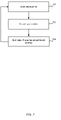
- the touch panel system which may comprise touch panel 600 , as shown in FIG. 6 , may detect the level of ambient IR (block 901 ) and if the detected level does not exceed a defined threshold (‘No’ in block 902 ), reflective mode is used (block 903 ) for the detection of touch events. However, if the detected level does exceed that threshold (‘Yes’ in block 902 ), shadow mode may be used instead (block 904 ). This decision may be taken on the basis of the whole panel (i.e.
- the decision may relate to portions of the panel (e.g. shadow mode is used for those portions of the display where the ambient IR exceeds the threshold).
- the portions may be of fixed size (e.g. the panel may be segmented into 6 portions and if the ambient IR at any point in that panel exceeds the threshold, then shadow mode is used for that portion) or of variable size (e.g. shadow mode is only used in the particular area where the ambient IR exceeds the threshold).
- the threshold (used in block 902 ) may be set based on a known maximum possible level of reflected IR.
- Shadow mode may be used to provide a low power mode of operation of the touch panel, as shown in FIG. 10 .
- This low power mode of operation may be used when the battery level falls below a certain level, when user enabled, during periods of inactivity or at any other time (referred to herein as ‘low power mode criteria’, assessed in block 1001 ).
- the touch panel may use shadow mode (block 904 ) during a period of inactivity (i.e.
- the IR sources may be illuminated for all or a part of the touch panel such that reflective mode can be used for detection of the touch event (block 903 ).
- the touch panel system may revert back to shadow mode (block 904 ).
- This low power mode may be enabled on the entire touch panel or on portions of the panel and the criteria may be assessed (in block 1001 ) on the basis of the entire panel or portions of the panel.
- aspects of these two techniques may be combined as shown in the example flow diagram of FIG. 11 such that the low power shadow mode is only able to be enabled (e.g. based on a period of inactivity or other criteria, as described above, determined in block 1001 ) where the ambient light exceeds a defined threshold (as determined in block 1101 ).
- a defined threshold as determined in block 1101 .
- the threshold used to determine whether a low power mode may be used (in block 1101 ) will be different to the threshold used to determine that reflective mode may be less suitable (in block 902 ), e.g. it will be set at a lower level of ambient IR. If the panel enters low power mode, the level of ambient light and the criteria for the low power mode may be monitored periodically or constantly, as indicated by the dotted arrow (from block 904 to block 1101 ).
- the decisions (in blocks 902 , 1001 , 1101 ) may be made by a control element within the touch panel system.
- the control element may be implemented using logic in hardware, or the control element may comprise a processor and memory (e.g. as shown in FIG. 17 and described below).
- the position of sensors detecting the reflected light in reflective mode may be offset from the actual position of the object on or adjacent to the touch panel.
- the sensors detecting the shadow caused by an object on or close to the touch panel may be different from those detecting the reflected light.
- Analysis of the different detection patterns in each mode obtained by modulating the IR sources and detecting the shadow in the periods when the IR source is off, may be used to obtain information on the distance between the object and the touch panel surface (referred to herein as ‘depth detection’) or to determine between a touch or no touch situation.
- depth detection information on the distance between the object and the touch panel surface
- Shadow mode instead of or in addition to reflective mode to detect depth (or to make touch/no touch decision) enables a more accurate detection because the curve on distance detection for reflective mode (i.e. power detected vs. distance) is not monotonic, whilst the corresponding curve for shadow mode is monotonic.
- Detection of touch/no touch may be implemented using an adaptive threshold, which may be adapted based on the detected ambient light level or based on the detection of an approaching object using shadow mode. In other examples, the detection may use two thresholds (one for reflective mode and one for shadow mode).
- multiple shadows may be cast by an object. In some circumstances this may provide additional 3D information about an object, e.g. as shown in FIG. 12 , with a first shape 1201 detected in reflective mode and a second shape 1202 detected on shadow mode.
- the object is, in this example, shaped like a pyramid.
- analysis of the two detected images may provide information on the approximate shape or thickness of the object (e.g. is it a planar object like a piece of paper or does it have substantial thickness like the gaming pieces shown in FIG. 1 ).
- the IR sources within the touch panel may be switched on and off (or modulated at higher speed) in groups such that the angle of illumination of an object changes dependent upon the group of sources which are switched on (e.g. odd columns/rows followed by even columns/rows).
- the illumination pattern may be varied based on the detected shape (e.g. to illuminate additional or different sources around the periphery of the detected shape).
- Analysis of the detected signals for each group of sources may provide some 3D information about the object (e.g. is it thin like a sheet of paper or does it have appreciable thickness), may improve the accuracy of the detected shape and may also enable the cancellation of any specular reflections e.g. due to the user wearing a ring. This may also reduce the overall power consumption of the touch panel system, which may be particularly useful where the system is battery operated and reduce interference caused by stray reflections within the touch panel.
- the position of the light source in the touch panel may be movable. By moving the source, the angle of illumination is again changed, therefore enabling detection of 3D information.
- the same effect may be achieved by moving a light guide which guides light from an IR source.
- the touch panel may control the ambient lighting.
- This control may, for example, use a Bluetooth, X10, IrDA (as described below) or other wireless link.
- the touch panel may control ambient light sources (which emit IR and may also emit visible light) so as to provide an optimised environment for use of shadow (or reflective) mode and/or to change the lighting angle to obtain depth/3D information, as described above.
- a computer vision system may be used to analyze the combined signals from the detectors within the system and control the ambient lighting based on the levels detected.
- the combined detected signals may be analyzed and the IR sources controlled based on the detected signals. This allows the touch panel to compensate for variations in IR ambient light across the touch panel which might otherwise degrade the sensing ability.
- the touch panel may further comprise an array of detectors which are sensitive to visible light.
- the combined detected signals from these visible light detectors may be analysed and used to control the brightness of parts of the image displayed on the touch panel. This may be achieved, for example, by changing the brightness of the back light or some of the LEDS in a LCD display. This enables the touch panel to compensate for variations in ambient visible light (e.g. due to sunlight or shadows on a portion of the display).
- the visible detectors (and sources) may also be used to assist in the identification of objects in proximity to the touch surfaces, as described above.
- the IR sources and/or sensors may be arranged to enable data communications between the screen and a nearby object.
- the communications may be unidirectional (in either direction) or bi-directional.
- the nearby object may be close to or in contact with the touch surface, or in other examples, the nearby object may be at a short distance from the touch screen (e.g. of the order of meters or tens of meters rather than kilometers).
- the touch panel 1300 which may comprise an array of infra-red detectors 1301 (e.g. IR sensitive TFTs or IR-sensitive photodiodes), may receive an IR signal from a nearby device 1302 including an IR transmitter 1303 .
- the operation, as shown in FIG. 14 involves the detection of the signal at one or more of the detectors (block 1401 ) and changing the display dependent upon the detected signal (block 1402 ).
- the display may be changed (in block 1402 ) in many different ways, for example:
- the signal transmitted by the nearby device 1302 may use any suitable protocol, such as the standard TV remote control protocol or IrDA.
- the shape of the beam projected by the nearby device may be controlled (e.g. a circle, square or cross-shaped) and may be fixed or variable.
- the change to the display e.g. the pointed icon displayed
- the shape detected may also be used to determine the location of the person holding the device with respect to the touch panel and where a cross-hair is used, the rotation of the device may be determined. This may enable the image displayed to change based on the user's location or an aspect of the game to be controlled based on the detected pointing parameters (e.g. shape, modulation scheme etc).
- aspects of the detected signal may, in some examples, be used to calibrate the response to signals received.
- the intensity of the detected signal may be used to determine the approximate distance between the device 1302 and the touch panel 1300 and the response to detected signals (in block 1402 ) may be changed based on this determination.
- the size of the expected gesture may be normalised based on the determined distance between the device and the touch panel.
- different devices may use different beam shapes, different wavelengths or different modulation (e.g. amplitude modulation) schemes.
- the signal may be modulated according to an identifier associated with the device (e.g. a Bluetooth MAC address) such that the information may be used to identify the device and for subsequent communication (e.g. by Bluetooth in this example).
- different pointing events may be distinguished using spatial multiplexing.
- the detected signal from multiple detectors may be analyzed (e.g. using a computer vision system) to determine whether two beams are being received (e.g. because there are two spatially separated groups of detectors which are detecting the signal or the shape detected is a partially overlapping combination of two known beam shapes).
- different nearby devices 1302 may be allocated different time slots for transmission of a pulsed IR signal (i.e. time division multiplexing) or different wavelengths may be used.
- Such a device 1302 may provide a user interface device for the touch panel.
- the touch panel may be arranged to interpret the detected shapes as user inputs (e.g. rotation of cross-hairs, gestures etc) and thereby control an application running on the display (e.g. use of gestures to move items between different displays). This may be combined with data communications between the touch panel and the device (e.g. if a user presses a button on the device) and this is described in detail below.
- Such a device may for example, provide a games controller and the detection of multiple pointing events, as described above, may provide means for multiple players to interact with the game via the touch panel substantially simultaneously.
- the nearby devices may comprise games controllers and the detection of multiple pointing events may enable a multiplayer shooting game to be played on the touch panel system.
- the device 1302 may also comprise a visible transmitter (not shown in FIG. 13 ) such as a visible laser or LED.
- a visible transmitter such as a visible laser or LED.
- the visible transmitter may be used for pointing and the IR transmitter may be used for data communications to control the application which is running.
- the application may be a presentation application (such as Microsoft PowerPoint (trade mark), a game or any other application.
- the signal received may comprise data (encoded in a modulated signal), rather than being a pointer signal.
- the modulated IR signal which comprises data may be received at one or more of the sensors 1301 in the touch panel (block 1501 ) and then stored (block 1502 ).
- spatial, frequency or time division multiplexing may be used in a similar manner to detection of multiple pointing events, as described above.
- any suitable protocol may be used, such as IrDA.
- the touch panel may transmit data to one or more nearby devices, as shown in the schematic diagram of FIG. 16 .
- the touch panel 1600 comprises, in addition to an array of IR sensitive detectors 1301 , one or more IR sources 1601 which may be used to illuminate nearby objects for use in reflective mode (as described above).
- One or more of the IR sources 1601 may be used to transmit data (indicated by beam 1602 ) to a nearby electronic device 1603 equipped with an IR receiver 1604 or a dedicated IR source may be provided for data transmission.
- the data may be broadcast such that all electronic devices which are within range can receive the data, or alternatively the data may be transmitted using different modulation schemes, or multiplexing techniques (e.g. spatial, frequency or time) in order to transmit different data to different devices.
- a DC-balanced encoding scheme is used for data transmission between the touch panel and one or more nearby devices. This data transmission is modulated at a rate faster than that required by the touch panel to detect a specified type of touch event, such as a fingertip touch. In this way, the touch panel is able to carry out data transmitting substantially simultaneously with touch event detection.
- the touch panel system is arranged to detect the outline of a nearby electronic device (such as 1302 of FIG. 13 ) either in reflective mode or shadow mode. This enables the touch panel system to detect the presence of the nearby electronic device and to “expect” possible data communication with that nearby device.
- the touch panel system may be arranged to switch at least some of the sensors within the detected outline into data communications mode.
- Whist the nearby devices in FIGS. 13 and 16 are depicted as a pointing device 1302 and a mobile telephone 1603 this is by way of example only and the touch panel may communicate with any nearby device comprising an IR transmitter and/or receiver.
- the devices may be located close to or in contact with the touch panel (e.g. intelligent game pieces) or at a distance from the touch panel (e.g. laptop or desktop computer, PDA, games console, games controller, light controller etc).
- the data transferred between a nearby device and the touch panel may be of any kind, including data for display on the touch panel, such as images captured on a digital camera (which may, for example, be integrated within a mobile telephone or PDA).
- the data transferred may be an identifier (e.g. the ID of a pointing device or the identifier for a particular data set which should be displayed on the touch panel).
- an identifier for a particular data set may be transmitted from the touch panel to a nearby device and then a gesture may be used to transfer that data set to another touch panel display system.
- the touch panel may only scan a subset of the sensors 1301 and upon detection of a signal (e.g. in block 1401 of FIG. 14 ), the panel may scan all the sensors 1301 in order to determine the full parameters of the signal (e.g. to determine the aspects of any gesture in detail).
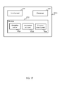
- FIG. 17 illustrates various components of an exemplary computing-based device 1700 which may be implemented as any form of a computing and/or electronic device, and in which embodiments of the methods and apparatus described above may be implemented.
- Computing-based device 1700 comprises a touch panel 1701 , for example as described above and shown in any of FIGS. 2 , 3 , 5 , 6 , 13 and 16 , and one or more processors 1702 .
- the one or more processors may be microprocessors, controllers or any other suitable type of processors for processing computing executable instructions to control the operation of the device in order to detect multiple touch/pointing events and/or to transmit or receive data to/from a nearby device.
- the computer executable instructions may be provided using any computer-readable media, such as memory 1703 .
- the memory is of any suitable type such as random access memory (RAM), a disk storage device of any type such as a magnetic or optical storage device, a hard disk drive, or a CD, DVD or other disc drive. Flash memory, EPROM or EEPROM may also be used.
- Platform software comprising an operating system 1704 or any other suitable platform software may be provided, and stored in memory 1703 , to enable application software 1705 to be executed on the device.
- the application software may include a computer vision system application 1706 .
- the computing-based device may also comprise one or more inputs which are of any suitable type for receiving media content, Internet Protocol (IP) input, user instructions from a user input device etc, a communication interface and one or more outputs such as an audio output.
- IP Internet Protocol
- the touch panel may use FTIR (frustrated total internal reflection) where the IR source emits a beam parallel to the touch surface and the IR sensors detect a drop in intensity.
- FTIR frustrated total internal reflection
- computer is used herein to refer to any device with processing capability such that it can execute instructions. Those skilled in the art will realize that such processing capabilities are incorporated into many different devices and therefore the term ‘computer’ includes PCs, servers, mobile telephones, personal digital assistants and many other devices.
- the methods described herein may be performed by software in machine readable form on a storage medium.
- the software can be suitable for execution on a parallel processor or a serial processor such that the method steps may be carried out in any suitable order, or simultaneously.
- a remote computer may store an example of the process described as software.
- a local or terminal computer may access the remote computer and download a part or all of the software to run the program.
- the local computer may download pieces of the software as needed, or execute some software instructions at the local terminal and some at the remote computer (or computer network).
- a dedicated circuit such as a DSP, programmable logic array, or the like.
Abstract
Description
-
- use of shadow mode for portions of the touch panel where the ambient light level exceeds a threshold
- use of shadow mode to provide a low power consumption mode
- use of both shadow mode and reflective mode to detect a particular object or to provide additional information about the object (e.g. depth, thickness etc)
- use of both shadow mode and reflective mode data to distinguish between touch and no touch events
Each of these are described in more detail below with reference toFIGS. 2 , 6 and 9-12.
-
- Display of a pointer icon on the touch panel dependent on the position of the detector receiving the signal. This provides a pointer system for use with a touch panel. This system may be used in many applications including presenting, gaming etc.
- Changing the user interface (UI) according to the detected pointing parameters (e.g. location, modulation scheme etc, as described in more detail below). This enables the movement of the device 1302 (e.g. when the user gestures or points) to be used to control the images/data displayed, navigation through various windows of a UI etc.
- Controlling the application running on the display system according to the pointing parameters.
Claims (10)
Priority Applications (5)
| Application Number | Priority Date | Filing Date | Title |
|---|---|---|---|
| US11/693,683 US8094129B2 (en) | 2006-11-27 | 2007-03-29 | Touch sensing using shadow and reflective modes |
| TW097111474A TWI475445B (en) | 2007-03-29 | 2008-03-28 | Method and touch panel system for touch sensing using shadow and reflective modes |
| PCT/US2008/058803 WO2008121906A1 (en) | 2007-03-29 | 2008-03-29 | Touch sensing using shadow and reflective modes |
| EP08744707A EP2130111A1 (en) | 2007-03-29 | 2008-03-29 | Touch sensing using shadow and reflective modes |
| US13/313,700 US8368663B2 (en) | 2006-11-27 | 2011-12-07 | Touch sensing using shadow and reflective modes |
Applications Claiming Priority (2)
| Application Number | Priority Date | Filing Date | Title |
|---|---|---|---|
| US11/604,491 US7924272B2 (en) | 2006-11-27 | 2006-11-27 | Infrared sensor integrated in a touch panel |
| US11/693,683 US8094129B2 (en) | 2006-11-27 | 2007-03-29 | Touch sensing using shadow and reflective modes |
Related Parent Applications (1)
| Application Number | Title | Priority Date | Filing Date |
|---|---|---|---|
| US11/604,491 Continuation-In-Part US7924272B2 (en) | 2006-11-27 | 2006-11-27 | Infrared sensor integrated in a touch panel |
Related Child Applications (1)
| Application Number | Title | Priority Date | Filing Date |
|---|---|---|---|
| US13/313,700 Continuation US8368663B2 (en) | 2006-11-27 | 2011-12-07 | Touch sensing using shadow and reflective modes |
Publications (2)
| Publication Number | Publication Date |
|---|---|
| US20080122803A1 US20080122803A1 (en) | 2008-05-29 |
| US8094129B2 true US8094129B2 (en) | 2012-01-10 |
Family
ID=39811409
Family Applications (2)
| Application Number | Title | Priority Date | Filing Date |
|---|---|---|---|
| US11/693,683 Expired - Fee Related US8094129B2 (en) | 2006-11-27 | 2007-03-29 | Touch sensing using shadow and reflective modes |
| US13/313,700 Expired - Fee Related US8368663B2 (en) | 2006-11-27 | 2011-12-07 | Touch sensing using shadow and reflective modes |
Family Applications After (1)
| Application Number | Title | Priority Date | Filing Date |
|---|---|---|---|
| US13/313,700 Expired - Fee Related US8368663B2 (en) | 2006-11-27 | 2011-12-07 | Touch sensing using shadow and reflective modes |
Country Status (4)
| Country | Link |
|---|---|
| US (2) | US8094129B2 (en) |
| EP (1) | EP2130111A1 (en) |
| TW (1) | TWI475445B (en) |
| WO (1) | WO2008121906A1 (en) |
Cited By (23)
| Publication number | Priority date | Publication date | Assignee | Title |
|---|---|---|---|---|
| US20100097352A1 (en) * | 2008-10-17 | 2010-04-22 | Samsung Mobile Display Co., Ltd. | Touch screen display and method of driving the same |
| US20100156821A1 (en) * | 2008-12-24 | 2010-06-24 | Hon Hai Precision Industry Co., Ltd. | Electronic device and method for detecting moving direction of inputs |
| US20110037730A1 (en) * | 2009-08-12 | 2011-02-17 | Au Optronics Corporation | Touch panel and touch display device having the same |
| US20110050599A1 (en) * | 2009-08-25 | 2011-03-03 | Hong Fu Jin Precision Industry (Shenzen) Co., Ltd. | Electronic device with touch input function and touch input method thereof |
| US20110157026A1 (en) * | 2009-12-30 | 2011-06-30 | Hong Kong Applied Science and Technology Research Institute Company Limited | Coordinate locating method, coordinate locating device, and display apparatus comprising the coordinate locating device |
| US20110157094A1 (en) * | 2006-11-27 | 2011-06-30 | Microsoft Corporation | Infrared sensor integrated in a touch panel |
| US20120038590A1 (en) * | 2010-08-12 | 2012-02-16 | Jee In Kim | Tabletop interface system and method thereof |
| US20120127127A1 (en) * | 2010-11-18 | 2012-05-24 | Microsoft Corporation | Single-camera display device detection |
| US20120170284A1 (en) * | 2010-12-30 | 2012-07-05 | Anna-Katrina Shedletsky | Diffuser and filter structures for light sensors |
| US20120218230A1 (en) * | 2009-11-05 | 2012-08-30 | Shanghai Jingyan Electronic Technology Co., Ltd. | Infrared touch screen device and multipoint locating method thereof |
| US8368663B2 (en) | 2006-11-27 | 2013-02-05 | Microsoft Corporation | Touch sensing using shadow and reflective modes |
| US8441702B2 (en) | 2009-11-24 | 2013-05-14 | International Business Machines Corporation | Scanning and capturing digital images using residue detection |
| US8610924B2 (en) | 2009-11-24 | 2013-12-17 | International Business Machines Corporation | Scanning and capturing digital images using layer detection |
| US8650634B2 (en) | 2009-01-14 | 2014-02-11 | International Business Machines Corporation | Enabling access to a subset of data |
| US20140192023A1 (en) * | 2013-01-10 | 2014-07-10 | Samsung Display Co., Ltd. | Proximity and touch sensing surface for integration with a display |
| US9360888B2 (en) | 2013-05-09 | 2016-06-07 | Stephen Howard | System and method for motion detection and interpretation |
| US9465488B2 (en) | 2013-05-09 | 2016-10-11 | Stephen Howard | System and method for motion detection and interpretation |
| US9817514B2 (en) | 2012-12-27 | 2017-11-14 | Flatfrog Laboratories Ab | Touch-sensing apparatus and a method for enabling control of a touch-sensing apparatus by an external device |
| US20180150669A1 (en) * | 2016-11-28 | 2018-05-31 | Nanchang O-Film Bio-Identification Technology Co., Ltd. | Organic light-enitting diode display panel for fingerprint recognition and electronic device |
| US10311802B2 (en) | 2015-08-19 | 2019-06-04 | Semiconductor Energy Laboratory Co., Ltd. | Information processing device |
| US10891003B2 (en) | 2013-05-09 | 2021-01-12 | Omni Consumer Products, Llc | System, method, and apparatus for an interactive container |
| US11048903B2 (en) | 2015-06-18 | 2021-06-29 | Shenzhen GOODIX Technology Co., Ltd. | Under-LCD screen optical sensor module for on-screen fingerprint sensing |
| US11233981B2 (en) | 2014-12-30 | 2022-01-25 | Omni Consumer Products, Llc | System and method for interactive projection |
Families Citing this family (345)
| Publication number | Priority date | Publication date | Assignee | Title |
|---|---|---|---|---|
| US6803906B1 (en) | 2000-07-05 | 2004-10-12 | Smart Technologies, Inc. | Passive touch system and method of detecting user input |
| US9164654B2 (en) | 2002-12-10 | 2015-10-20 | Neonode Inc. | User interface for mobile computer unit |
| SE0103835L (en) * | 2001-11-02 | 2003-05-03 | Neonode Ab | Touch screen realized by display unit with light transmitting and light receiving units |
| US9052777B2 (en) | 2001-11-02 | 2015-06-09 | Neonode Inc. | Optical elements with alternating reflective lens facets |
| US8674966B2 (en) | 2001-11-02 | 2014-03-18 | Neonode Inc. | ASIC controller for light-based touch screen |
| US8339379B2 (en) * | 2004-04-29 | 2012-12-25 | Neonode Inc. | Light-based touch screen |
| US9778794B2 (en) | 2001-11-02 | 2017-10-03 | Neonode Inc. | Light-based touch screen |
| US9213443B2 (en) | 2009-02-15 | 2015-12-15 | Neonode Inc. | Optical touch screen systems using reflected light |
| US9052771B2 (en) | 2002-11-04 | 2015-06-09 | Neonode Inc. | Touch screen calibration and update methods |
| US9471170B2 (en) | 2002-11-04 | 2016-10-18 | Neonode Inc. | Light-based touch screen with shift-aligned emitter and receiver lenses |
| US8416217B1 (en) | 2002-11-04 | 2013-04-09 | Neonode Inc. | Light-based finger gesture user interface |
| US8896575B2 (en) | 2002-11-04 | 2014-11-25 | Neonode Inc. | Pressure-sensitive touch screen |
| US8587562B2 (en) | 2002-11-04 | 2013-11-19 | Neonode Inc. | Light-based touch screen using elliptical and parabolic reflectors |
| US6954197B2 (en) | 2002-11-15 | 2005-10-11 | Smart Technologies Inc. | Size/scale and orientation determination of a pointer in a camera-based touch system |
| US8403203B2 (en) * | 2002-12-10 | 2013-03-26 | Neonoda Inc. | Component bonding using a capillary effect |
| US9195344B2 (en) | 2002-12-10 | 2015-11-24 | Neonode Inc. | Optical surface using a reflected image for determining three-dimensional position information |
| US9389730B2 (en) * | 2002-12-10 | 2016-07-12 | Neonode Inc. | Light-based touch screen using elongated light guides |
| US8902196B2 (en) | 2002-12-10 | 2014-12-02 | Neonode Inc. | Methods for determining a touch location on a touch screen |
| US7629967B2 (en) | 2003-02-14 | 2009-12-08 | Next Holdings Limited | Touch screen signal processing |
| US8456447B2 (en) | 2003-02-14 | 2013-06-04 | Next Holdings Limited | Touch screen signal processing |
| US8508508B2 (en) | 2003-02-14 | 2013-08-13 | Next Holdings Limited | Touch screen signal processing with single-point calibration |
| CA2419704A1 (en) | 2003-02-24 | 2004-08-24 | Ignis Innovation Inc. | Method of manufacturing a pixel with organic light-emitting diode |
| US7532206B2 (en) | 2003-03-11 | 2009-05-12 | Smart Technologies Ulc | System and method for differentiating between pointers used to contact touch surface |
| US7411575B2 (en) * | 2003-09-16 | 2008-08-12 | Smart Technologies Ulc | Gesture recognition method and touch system incorporating the same |
| US7274356B2 (en) * | 2003-10-09 | 2007-09-25 | Smart Technologies Inc. | Apparatus for determining the location of a pointer within a region of interest |
| US7355593B2 (en) | 2004-01-02 | 2008-04-08 | Smart Technologies, Inc. | Pointer tracking across multiple overlapping coordinate input sub-regions defining a generally contiguous input region |
| US8291762B2 (en) | 2004-01-15 | 2012-10-23 | Robert Akins | Work capacities testing apparatus and method |
| US7460110B2 (en) | 2004-04-29 | 2008-12-02 | Smart Technologies Ulc | Dual mode touch system |
| US7538759B2 (en) | 2004-05-07 | 2009-05-26 | Next Holdings Limited | Touch panel display system with illumination and detection provided from a single edge |
| US8120596B2 (en) | 2004-05-21 | 2012-02-21 | Smart Technologies Ulc | Tiled touch system |
| CA2495726A1 (en) | 2005-01-28 | 2006-07-28 | Ignis Innovation Inc. | Locally referenced voltage programmed pixel for amoled displays |
| JP4725482B2 (en) * | 2006-10-16 | 2011-07-13 | カシオ計算機株式会社 | Photosensor, photosensor target detection method and display device |
| US8269746B2 (en) * | 2006-11-27 | 2012-09-18 | Microsoft Corporation | Communication with a touch screen |
| US9442607B2 (en) | 2006-12-04 | 2016-09-13 | Smart Technologies Inc. | Interactive input system and method |
| US8115753B2 (en) | 2007-04-11 | 2012-02-14 | Next Holdings Limited | Touch screen system with hover and click input methods |
| EP2165248A4 (en) * | 2007-07-06 | 2011-11-23 | Neonode Inc | Scanning of a touch screen |
| JP2009026155A (en) * | 2007-07-20 | 2009-02-05 | Toshiba Corp | Input display apparatus and mobile wireless terminal apparatus |
| US8094137B2 (en) | 2007-07-23 | 2012-01-10 | Smart Technologies Ulc | System and method of detecting contact on a display |
| JP2009032005A (en) * | 2007-07-26 | 2009-02-12 | Toshiba Corp | Input display device and input display panel |
| CA2697856A1 (en) | 2007-08-30 | 2009-03-05 | Next Holdings, Inc. | Low profile touch panel systems |
| WO2009029767A1 (en) | 2007-08-30 | 2009-03-05 | Next Holdings, Inc. | Optical touchscreen with improved illumination |
| US9134904B2 (en) * | 2007-10-06 | 2015-09-15 | International Business Machines Corporation | Displaying documents to a plurality of users of a surface computer |
| US8139036B2 (en) * | 2007-10-07 | 2012-03-20 | International Business Machines Corporation | Non-intrusive capture and display of objects based on contact locality |
| US20090091539A1 (en) * | 2007-10-08 | 2009-04-09 | International Business Machines Corporation | Sending A Document For Display To A User Of A Surface Computer |
| US20090091529A1 (en) * | 2007-10-09 | 2009-04-09 | International Business Machines Corporation | Rendering Display Content On A Floor Surface Of A Surface Computer |
| US8024185B2 (en) * | 2007-10-10 | 2011-09-20 | International Business Machines Corporation | Vocal command directives to compose dynamic display text |
| US8439756B2 (en) | 2007-11-09 | 2013-05-14 | Igt | Gaming system having a display/input device configured to interactively operate with external device |
| US8545321B2 (en) | 2007-11-09 | 2013-10-01 | Igt | Gaming system having user interface with uploading and downloading capability |
| US7976372B2 (en) | 2007-11-09 | 2011-07-12 | Igt | Gaming system having multiple player simultaneous display/input device |
| JP4475321B2 (en) * | 2007-11-26 | 2010-06-09 | ソニー株式会社 | Display device |
| US9203833B2 (en) * | 2007-12-05 | 2015-12-01 | International Business Machines Corporation | User authorization using an automated Turing Test |
| JP5301240B2 (en) * | 2007-12-05 | 2013-09-25 | 株式会社ジャパンディスプレイウェスト | Display device |
| BRPI0821156A2 (en) * | 2007-12-20 | 2015-06-16 | Sharp Kk | Tendfo optical sensors display device |
| US8405636B2 (en) | 2008-01-07 | 2013-03-26 | Next Holdings Limited | Optical position sensing system and optical position sensor assembly |
| CN101842765B (en) * | 2008-01-25 | 2012-11-07 | 夏普株式会社 | Display device provided with optical sensor |
| BRPI0821423A2 (en) * | 2008-01-31 | 2015-06-16 | Sharp Kk | Visual presentation device and active matrix substrate. |
| TWI380202B (en) * | 2008-02-19 | 2012-12-21 | Wintek Corp | Driving method |
| JPWO2009104667A1 (en) * | 2008-02-21 | 2011-06-23 | シャープ株式会社 | Display device with optical sensor |
| JP5208198B2 (en) * | 2008-03-03 | 2013-06-12 | シャープ株式会社 | Display device with optical sensor |
| WO2009110293A1 (en) * | 2008-03-03 | 2009-09-11 | シャープ株式会社 | Display device with light sensors |
| TW200939754A (en) * | 2008-03-04 | 2009-09-16 | Qisda Corp | Display device |
| KR101493840B1 (en) * | 2008-03-14 | 2015-02-17 | 삼성디스플레이 주식회사 | Liquid crystal display, display system and method for recognizing shape of object using the liquid crystal display |
| US8902193B2 (en) | 2008-05-09 | 2014-12-02 | Smart Technologies Ulc | Interactive input system and bezel therefor |
| US20100060611A1 (en) * | 2008-09-05 | 2010-03-11 | Sony Ericsson Mobile Communication Ab | Touch display with switchable infrared illumination for touch position determination and methods thereof |
| US8529345B2 (en) | 2008-10-02 | 2013-09-10 | Igt | Gaming system including a gaming table with mobile user input devices |
| US8346330B2 (en) | 2008-10-13 | 2013-01-01 | Masimo Corporation | Reflection-detector sensor position indicator |
| US9323410B2 (en) * | 2008-10-13 | 2016-04-26 | Sony Ericsson Mobile Communications Ab | User input displays for mobile devices |
| US8154532B2 (en) * | 2008-10-15 | 2012-04-10 | Au Optronics Corporation | LCD display with photo sensor touch function |
| KR101015883B1 (en) * | 2008-10-17 | 2011-02-23 | 삼성모바일디스플레이주식회사 | Touch screen display apparatus and method for driving the same |
| KR101337042B1 (en) * | 2008-10-21 | 2013-12-05 | 엘지디스플레이 주식회사 | Touch panel display device and driving method thereof |
| US8339378B2 (en) | 2008-11-05 | 2012-12-25 | Smart Technologies Ulc | Interactive input system with multi-angle reflector |
| US8860696B2 (en) * | 2008-11-12 | 2014-10-14 | Flatfrog Laboratories Ab | Integrated touch-sensing display apparatus and method of operating the same |
| US8797274B2 (en) * | 2008-11-30 | 2014-08-05 | Lenovo (Singapore) Pte. Ltd. | Combined tap sequence and camera based user interface |
| SE533704C2 (en) | 2008-12-05 | 2010-12-07 | Flatfrog Lab Ab | Touch sensitive apparatus and method for operating the same |
| JP4650703B2 (en) * | 2008-12-25 | 2011-03-16 | ソニー株式会社 | Display panel, module and electronic device |
| JP4798218B2 (en) * | 2008-12-26 | 2011-10-19 | ブラザー工業株式会社 | Telephone device |
| US8030914B2 (en) * | 2008-12-29 | 2011-10-04 | Motorola Mobility, Inc. | Portable electronic device having self-calibrating proximity sensors |
| US8275412B2 (en) * | 2008-12-31 | 2012-09-25 | Motorola Mobility Llc | Portable electronic device having directional proximity sensors based on device orientation |
| TWI397005B (en) * | 2009-01-07 | 2013-05-21 | Elan Microelectronics Corp | Ghost Detection Method for Capacitive Touchpad |
| US20100201275A1 (en) * | 2009-02-06 | 2010-08-12 | Cok Ronald S | Light sensing in display device |
| US9063614B2 (en) | 2009-02-15 | 2015-06-23 | Neonode Inc. | Optical touch screens |
| US8775023B2 (en) | 2009-02-15 | 2014-07-08 | Neanode Inc. | Light-based touch controls on a steering wheel and dashboard |
| DE102009009316A1 (en) * | 2009-02-17 | 2010-08-26 | Infineon Technologies Ag | Photodetector semiconductor device, photoemitter semiconductor device, optoelectronic transmission system, and method of transmitting an electrical signal |
| KR101617645B1 (en) * | 2009-02-24 | 2016-05-04 | 삼성전자주식회사 | Method for controlling display and apparatus using the same |
| JP4683135B2 (en) * | 2009-03-04 | 2011-05-11 | エプソンイメージングデバイス株式会社 | Display device with position detection function and electronic device |
| JP4699536B2 (en) * | 2009-03-06 | 2011-06-15 | シャープ株式会社 | POSITION DETECTION DEVICE, CONTROL METHOD, CONTROL PROGRAM, AND RECORDING MEDIUM |
| US20100245289A1 (en) * | 2009-03-31 | 2010-09-30 | Miroslav Svajda | Apparatus and method for optical proximity sensing and touch input control |
| JP5615904B2 (en) * | 2009-04-16 | 2014-10-29 | ネオノード インコーポレイテッド | Optical touch screen system using reflected light |
| US20100271331A1 (en) * | 2009-04-22 | 2010-10-28 | Rachid Alameh | Touch-Screen and Method for an Electronic Device |
| US20100295821A1 (en) * | 2009-05-20 | 2010-11-25 | Tom Chang | Optical touch panel |
| US8304733B2 (en) * | 2009-05-22 | 2012-11-06 | Motorola Mobility Llc | Sensing assembly for mobile device |
| US8294105B2 (en) * | 2009-05-22 | 2012-10-23 | Motorola Mobility Llc | Electronic device with sensing assembly and method for interpreting offset gestures |
| US8788676B2 (en) | 2009-05-22 | 2014-07-22 | Motorola Mobility Llc | Method and system for controlling data transmission to or from a mobile device |
| US8269175B2 (en) * | 2009-05-22 | 2012-09-18 | Motorola Mobility Llc | Electronic device with sensing assembly and method for detecting gestures of geometric shapes |
| US20140078318A1 (en) * | 2009-05-22 | 2014-03-20 | Motorola Mobility Llc | Electronic Device with Sensing Assembly and Method for Interpreting Consecutive Gestures |
| US8542186B2 (en) | 2009-05-22 | 2013-09-24 | Motorola Mobility Llc | Mobile device with user interaction capability and method of operating same |
| US8391719B2 (en) * | 2009-05-22 | 2013-03-05 | Motorola Mobility Llc | Method and system for conducting communication between mobile devices |
| US8619029B2 (en) | 2009-05-22 | 2013-12-31 | Motorola Mobility Llc | Electronic device with sensing assembly and method for interpreting consecutive gestures |
| US8344325B2 (en) * | 2009-05-22 | 2013-01-01 | Motorola Mobility Llc | Electronic device with sensing assembly and method for detecting basic gestures |
| TWI410703B (en) * | 2009-06-18 | 2013-10-01 | Au Optronics Corp | Photo sensor, method of forming the same, and optical touch device |
| TWI433310B (en) * | 2009-07-02 | 2014-04-01 | Au Optronics Corp | Organic light emitting diode touch display |
| CN101943973A (en) * | 2009-07-03 | 2011-01-12 | 北京汇冠新技术股份有限公司 | Interactive display |
| CN101943972A (en) * | 2009-07-03 | 2011-01-12 | 北京汇冠新技术股份有限公司 | Touch screen |
| WO2011004135A1 (en) | 2009-07-07 | 2011-01-13 | Elliptic Laboratories As | Control using movements |
| US8319170B2 (en) * | 2009-07-10 | 2012-11-27 | Motorola Mobility Llc | Method for adapting a pulse power mode of a proximity sensor |
| US9274547B2 (en) | 2009-07-23 | 2016-03-01 | Hewlett-Packard Development Compamy, L.P. | Display with an optical sensor |
| DE112009004947T5 (en) * | 2009-07-23 | 2012-07-12 | Hewlett-Packard Development Co., L.P. | Display with an optical sensor |
| EP2287711A1 (en) * | 2009-08-05 | 2011-02-23 | Nlighten Trading (Shanghai) Co. | Extended infrared-sourced multi-touch screen |
| JP5273676B2 (en) * | 2009-08-10 | 2013-08-28 | ヌライテン トレーディング (シャンハイ)カンパニー | Wide-area infrared light source multi-touch screen |
| KR20110019238A (en) * | 2009-08-19 | 2011-02-25 | 삼성전자주식회사 | Touch panel |
| US8902195B2 (en) * | 2009-09-01 | 2014-12-02 | Smart Technologies Ulc | Interactive input system with improved signal-to-noise ratio (SNR) and image capture method |
| SE534244C2 (en) | 2009-09-02 | 2011-06-14 | Flatfrog Lab Ab | Touch sensitive system and method for functional control thereof |
| CN102597936B (en) * | 2009-09-02 | 2015-01-07 | 平蛙实验室股份公司 | Touch surface with a compensated signal profile |
| KR101073345B1 (en) * | 2009-10-06 | 2011-10-14 | 삼성모바일디스플레이주식회사 | Liquid Crystal Display with a Built-in Touch Screen |
| KR101073194B1 (en) * | 2009-10-06 | 2011-10-12 | 삼성모바일디스플레이주식회사 | Liquid Crystal Display with a Built-in Touch Screen |
| EP2491480A4 (en) * | 2009-10-19 | 2014-07-30 | Flatfrog Lab Ab | Touch surface with two-dimensional compensation |
| US9430079B2 (en) | 2009-10-19 | 2016-08-30 | Flatfrog Laboratories Ab | Determining touch data for one or more objects on a touch surface |
| WO2011049511A1 (en) | 2009-10-19 | 2011-04-28 | Flatfrog Laboratories Ab | Extracting touch data that represents one or more objects on a touch surface |
| KR101264728B1 (en) * | 2009-10-23 | 2013-05-15 | 엘지디스플레이 주식회사 | Liquid Crystal Display Device |
| KR101843561B1 (en) * | 2009-10-26 | 2018-03-30 | 가부시키가이샤 한도오따이 에네루기 켄큐쇼 | Display device and semiconductor device |
| US8283967B2 (en) | 2009-11-12 | 2012-10-09 | Ignis Innovation Inc. | Stable current source for system integration to display substrate |
| US8446392B2 (en) * | 2009-11-16 | 2013-05-21 | Smart Technologies Ulc | Method for determining the location of a pointer in a pointer input region, and interactive input system executing the method |
| US8622742B2 (en) * | 2009-11-16 | 2014-01-07 | Microsoft Corporation | Teaching gestures with offset contact silhouettes |
| US20110117526A1 (en) * | 2009-11-16 | 2011-05-19 | Microsoft Corporation | Teaching gesture initiation with registration posture guides |
| US8665227B2 (en) | 2009-11-19 | 2014-03-04 | Motorola Mobility Llc | Method and apparatus for replicating physical key function with soft keys in an electronic device |
| KR101652110B1 (en) * | 2009-12-03 | 2016-08-29 | 엘지전자 주식회사 | Controlling power of devices which is controllable with user's gesture |
| KR101642146B1 (en) * | 2009-12-07 | 2016-07-29 | 엘지이노텍 주식회사 | Touch screen display apparatus |
| KR101672343B1 (en) * | 2009-12-10 | 2016-11-04 | 삼성전자주식회사 | Optical touch panel and Method of driving the same |
| TWI522869B (en) * | 2009-12-17 | 2016-02-21 | 中強光電股份有限公司 | Optical touch display apparatus |
| TWI492128B (en) * | 2009-12-22 | 2015-07-11 | Coretronic Corp | Optical touch display apparatus |
| TWI412948B (en) * | 2009-12-31 | 2013-10-21 | Ind Tech Res Inst | Collision simulating method of three dimensional object |
| TWI430153B (en) * | 2010-01-07 | 2014-03-11 | Chunghwa Picture Tubes Ltd | Touch panel and touch sensing method |
| FR2955403B1 (en) * | 2010-01-20 | 2016-07-29 | Neocreativ | CONTROL DEVICE AND ELECTRONIC DEVICE COMPRISING SAME |
| TWI594173B (en) * | 2010-03-08 | 2017-08-01 | 半導體能源研究所股份有限公司 | Electronic device and electronic system |
| KR20110103140A (en) * | 2010-03-12 | 2011-09-20 | 삼성전자주식회사 | Apparatus for multi touch and proximated object sensing by irradiating light selectively |
| KR101065408B1 (en) * | 2010-03-17 | 2011-09-16 | 삼성모바일디스플레이주식회사 | Touch controlled display device |
| US9268478B2 (en) * | 2010-03-31 | 2016-02-23 | Honeywell International Inc. | Touch screen system for use with a commanded system requiring high integrity |
| WO2011121484A1 (en) * | 2010-03-31 | 2011-10-06 | Koninklijke Philips Electronics N.V. | Head-pose tracking system |
| FR2958426B1 (en) * | 2010-04-02 | 2012-10-26 | Alain Jutant | MULTI-POINT AND MULTI-USER INTERACTIVE SCREEN. |
| KR101652786B1 (en) * | 2010-04-22 | 2016-09-12 | 삼성전자주식회사 | Simplified light sensing circuit, and remote optical touch panel and image acquisition apparatus employing the circuit |
| US9891102B2 (en) | 2010-04-22 | 2018-02-13 | Samsung Electronics Co., Ltd. | Simplified light sensing circuit, light sensing apparatus including the light sensing circuit, method of driving the light sensing apparatus, and image acquisition apparatus and optical touch screen apparatus including the light sensing apparatus |
| TW201203052A (en) | 2010-05-03 | 2012-01-16 | Flatfrog Lab Ab | Touch determination by tomographic reconstruction |
| US8963845B2 (en) | 2010-05-05 | 2015-02-24 | Google Technology Holdings LLC | Mobile device with temperature sensing capability and method of operating same |
| US8878773B1 (en) | 2010-05-24 | 2014-11-04 | Amazon Technologies, Inc. | Determining relative motion as input |
| US9103732B2 (en) | 2010-05-25 | 2015-08-11 | Google Technology Holdings LLC | User computer device with temperature sensing capabilities and method of operating same |
| US8751056B2 (en) | 2010-05-25 | 2014-06-10 | Motorola Mobility Llc | User computer device with temperature sensing capabilities and method of operating same |
| TWI409679B (en) * | 2010-06-04 | 2013-09-21 | Au Optronics Corp | Optical touch panel and touch display panel and touch input method thereof |
| US20110310005A1 (en) * | 2010-06-17 | 2011-12-22 | Qualcomm Incorporated | Methods and apparatus for contactless gesture recognition |
| TW201201077A (en) * | 2010-06-18 | 2012-01-01 | Nlighten Trading Shanghai Co Ltd | A light uniforming system of projected touch technology |
| TW201205386A (en) * | 2010-07-21 | 2012-02-01 | Pixart Imaging Inc | Touch system and touch sensing method |
| CN102339167A (en) * | 2010-07-22 | 2012-02-01 | 原相科技股份有限公司 | Touch-control system and touch-control detection method |
| TWI436322B (en) | 2010-09-14 | 2014-05-01 | Ind Tech Res Inst | Photosensitive circuit and system for photosensitive display |
| EP2617024A4 (en) * | 2010-09-17 | 2014-06-04 | Nokia Corp | Adjustment of display brightness |
| KR101750990B1 (en) * | 2010-10-04 | 2017-07-12 | 삼성디스플레이 주식회사 | Display apparatus and method of driving the same |
| AT510044B1 (en) * | 2010-10-06 | 2012-01-15 | Isiqiri Interface Tech Gmbh | CURTAIN |
| US8514190B2 (en) * | 2010-10-06 | 2013-08-20 | Sony Corporation | Displays for electronic devices that detect and respond to the contour and/or height profile of user input objects |
| CN102486702A (en) * | 2010-12-01 | 2012-06-06 | 敦南科技股份有限公司 | Reflection-type optical sensing device and electronic device |
| KR20120060407A (en) * | 2010-12-02 | 2012-06-12 | 삼성전자주식회사 | Display substrate, method of manufacturing the same and touch display apparatus having the display substrate |
| US20120162126A1 (en) * | 2010-12-22 | 2012-06-28 | Chih-Ming Yuan | Touch-sensing display device |
| CN102662527B (en) * | 2010-12-22 | 2015-08-26 | 剑扬股份有限公司 | Touch-control sensing display device |
| KR20120073763A (en) | 2010-12-27 | 2012-07-05 | 삼성전자주식회사 | Display apparatus |
| US8635560B2 (en) * | 2011-01-21 | 2014-01-21 | Blackberry Limited | System and method for reducing power consumption in an electronic device having a touch-sensitive display |
| US8730209B2 (en) * | 2011-01-21 | 2014-05-20 | Motorola Mobility Llc | Method for resolving blind spots associated with proximity sensors |
| KR101770969B1 (en) * | 2011-01-21 | 2017-08-25 | 삼성디스플레이 주식회사 | Substrate of sensing touch and method of manufacturing the substrate |
| WO2012112707A1 (en) * | 2011-02-15 | 2012-08-23 | Cirque Corporation | Reduction of noise and de-ghosting in a mutual capacitance multi -touch touchpad |
| JP2012185798A (en) * | 2011-02-16 | 2012-09-27 | Ricoh Co Ltd | Coordinate detection system, information processor, method, program and recording medium |
| KR101765771B1 (en) * | 2011-05-05 | 2017-08-07 | 맥심 인터그래이티드 프로덕츠 인코포레이티드 | Method for detecting gestures using a multi-segment photodiode and one or fewer illumination sources |
| US9606607B2 (en) | 2011-05-17 | 2017-03-28 | Ignis Innovation Inc. | Systems and methods for display systems with dynamic power control |
| US20120320216A1 (en) * | 2011-06-14 | 2012-12-20 | Disney Enterprises, Inc. | Method and System for Object Recognition, Authentication, and Tracking with Infrared Distortion Caused by Objects for Augmented Reality |
| GB201110159D0 (en) * | 2011-06-16 | 2011-07-27 | Light Blue Optics Ltd | Touch sensitive display devices |
| US9041734B2 (en) | 2011-07-12 | 2015-05-26 | Amazon Technologies, Inc. | Simulating three-dimensional features |
| US8901579B2 (en) | 2011-08-03 | 2014-12-02 | Ignis Innovation Inc. | Organic light emitting diode and method of manufacturing |
| US10088924B1 (en) | 2011-08-04 | 2018-10-02 | Amazon Technologies, Inc. | Overcoming motion effects in gesture recognition |
| TWI454996B (en) * | 2011-08-18 | 2014-10-01 | Au Optronics Corp | Display and method of determining a position of an object applied to a three-dimensional interactive display |
| US8947351B1 (en) * | 2011-09-27 | 2015-02-03 | Amazon Technologies, Inc. | Point of view determinations for finger tracking |
| WO2013081894A1 (en) * | 2011-11-28 | 2013-06-06 | Corning Incorporated | Optical touch-screen systems and methods using a planar transparent sheet |
| US10089924B2 (en) | 2011-11-29 | 2018-10-02 | Ignis Innovation Inc. | Structural and low-frequency non-uniformity compensation |
| US9385169B2 (en) | 2011-11-29 | 2016-07-05 | Ignis Innovation Inc. | Multi-functional active matrix organic light-emitting diode display |
| US9063591B2 (en) | 2011-11-30 | 2015-06-23 | Google Technology Holdings LLC | Active styluses for interacting with a mobile device |
| US8963885B2 (en) | 2011-11-30 | 2015-02-24 | Google Technology Holdings LLC | Mobile device for interacting with an active stylus |
| US8942434B1 (en) | 2011-12-20 | 2015-01-27 | Amazon Technologies, Inc. | Conflict resolution for pupil detection |
| US8982090B2 (en) * | 2012-01-01 | 2015-03-17 | Cypress Semiconductor Corporation | Optical stylus synchronization |
| US9223415B1 (en) | 2012-01-17 | 2015-12-29 | Amazon Technologies, Inc. | Managing resource usage for task performance |
| US9064451B2 (en) | 2012-02-01 | 2015-06-23 | Apple Inc. | Organic light emitting diode display having photodiodes |
| US9052414B2 (en) | 2012-02-07 | 2015-06-09 | Microsoft Technology Licensing, Llc | Virtual image device |
| US9354748B2 (en) | 2012-02-13 | 2016-05-31 | Microsoft Technology Licensing, Llc | Optical stylus interaction |
| US20130222353A1 (en) * | 2012-02-29 | 2013-08-29 | Microsoft Corporation | Prism illumination-optic |
| US8749529B2 (en) | 2012-03-01 | 2014-06-10 | Microsoft Corporation | Sensor-in-pixel display system with near infrared filter |
| US8873227B2 (en) | 2012-03-02 | 2014-10-28 | Microsoft Corporation | Flexible hinge support layer |
| US9460029B2 (en) | 2012-03-02 | 2016-10-04 | Microsoft Technology Licensing, Llc | Pressure sensitive keys |
| US9870066B2 (en) | 2012-03-02 | 2018-01-16 | Microsoft Technology Licensing, Llc | Method of manufacturing an input device |
| US9075566B2 (en) | 2012-03-02 | 2015-07-07 | Microsoft Technoogy Licensing, LLC | Flexible hinge spine |
| US9298236B2 (en) | 2012-03-02 | 2016-03-29 | Microsoft Technology Licensing, Llc | Multi-stage power adapter configured to provide a first power level upon initial connection of the power adapter to the host device and a second power level thereafter upon notification from the host device to the power adapter |
| US9122354B2 (en) * | 2012-03-14 | 2015-09-01 | Texas Instruments Incorporated | Detecting wave gestures near an illuminated surface |
| JP5337268B2 (en) * | 2012-03-30 | 2013-11-06 | 株式会社東芝 | Operation display device and operation display method |
| US20130300590A1 (en) | 2012-05-14 | 2013-11-14 | Paul Henry Dietz | Audio Feedback |
| US10168835B2 (en) | 2012-05-23 | 2019-01-01 | Flatfrog Laboratories Ab | Spatial resolution in touch displays |
| US20130314377A1 (en) * | 2012-05-25 | 2013-11-28 | Oleg Los | Optical touch sensor apparatus |
| US9317113B1 (en) | 2012-05-31 | 2016-04-19 | Amazon Technologies, Inc. | Gaze assisted object recognition |
| US10031556B2 (en) | 2012-06-08 | 2018-07-24 | Microsoft Technology Licensing, Llc | User experience adaptation |
| US8947353B2 (en) | 2012-06-12 | 2015-02-03 | Microsoft Corporation | Photosensor array gesture detection |
| US9019615B2 (en) | 2012-06-12 | 2015-04-28 | Microsoft Technology Licensing, Llc | Wide field-of-view virtual image projector |
| US9256089B2 (en) * | 2012-06-15 | 2016-02-09 | Microsoft Technology Licensing, Llc | Object-detecting backlight unit |
| US20130342493A1 (en) * | 2012-06-20 | 2013-12-26 | Microsoft Corporation | Touch Detection on a Compound Curve Surface |
| US20150123938A1 (en) * | 2012-07-06 | 2015-05-07 | Freescale Semiconductor, Inc. | Electronic device for proximity detection, a light emitting diode for such electronic device, a control unit for such electronic device, an apparatus comprising such electronic device and an associated method |
| US9767446B2 (en) * | 2012-07-19 | 2017-09-19 | Mastercard International Incorporated | Touch screen system and methods for multiple contactless payments |
| US9355345B2 (en) | 2012-07-23 | 2016-05-31 | Microsoft Technology Licensing, Llc | Transparent tags with encoded data |
| GB2504291A (en) * | 2012-07-24 | 2014-01-29 | St Microelectronics Ltd | A proximity and gesture detection module |
| US8964379B2 (en) | 2012-08-20 | 2015-02-24 | Microsoft Corporation | Switchable magnetic lock |
| US9262010B2 (en) | 2012-09-05 | 2016-02-16 | Synaptics Incorporated | Systems and methods for reducing effects of interference in input devices |
| TWI467446B (en) * | 2012-09-28 | 2015-01-01 | Au Optronics Corp | Optical touch pad and brightness control method thereof |
| US9152173B2 (en) | 2012-10-09 | 2015-10-06 | Microsoft Technology Licensing, Llc | Transparent display device |
| US20140098063A1 (en) * | 2012-10-10 | 2014-04-10 | Research In Motion Limited | Electronic device with proximity sensing |
| US9921661B2 (en) | 2012-10-14 | 2018-03-20 | Neonode Inc. | Optical proximity sensor and associated user interface |
| US9164625B2 (en) | 2012-10-14 | 2015-10-20 | Neonode Inc. | Proximity sensor for determining two-dimensional coordinates of a proximal object |
| US9207800B1 (en) | 2014-09-23 | 2015-12-08 | Neonode Inc. | Integrated light guide and touch screen frame and multi-touch determination method |
| US10282034B2 (en) | 2012-10-14 | 2019-05-07 | Neonode Inc. | Touch sensitive curved and flexible displays |
| TWI461896B (en) * | 2012-11-07 | 2014-11-21 | Chih Chung Lin | Touch panel with photovoltaic conversion function |
| US9513748B2 (en) | 2012-12-13 | 2016-12-06 | Microsoft Technology Licensing, Llc | Combined display panel circuit |
| FR3001063B1 (en) * | 2013-01-15 | 2015-02-13 | Commissariat Energie Atomique | SYSTEM AND METHOD FOR DETECTING THE POSITION OF AN ACTUATION MEMBER ON A DISPLAY SCREEN |
| FR3001064B1 (en) * | 2013-01-15 | 2015-02-13 | Commissariat Energie Atomique | SYSTEM AND METHOD FOR DETECTING THE POSITION OF AN ACTUATION MEMBER ON A DISPLAY SCREEN |
| WO2014112995A1 (en) * | 2013-01-16 | 2014-07-24 | Blackberry Limited | Electronic device with touch-sensitive display and gesture-detection |
| US9323380B2 (en) | 2013-01-16 | 2016-04-26 | Blackberry Limited | Electronic device with touch-sensitive display and three-dimensional gesture-detection |
| US9335922B2 (en) | 2013-01-16 | 2016-05-10 | Research In Motion Limited | Electronic device including three-dimensional gesture detecting display |
| WO2014112994A1 (en) * | 2013-01-16 | 2014-07-24 | Blackberry Limited | Electronic device including three-dimensional gesture detecting display |
| US9638835B2 (en) | 2013-03-05 | 2017-05-02 | Microsoft Technology Licensing, Llc | Asymmetric aberration correcting lens |
| US9721505B2 (en) | 2013-03-08 | 2017-08-01 | Ignis Innovation Inc. | Pixel circuits for AMOLED displays |
| US9465484B1 (en) * | 2013-03-11 | 2016-10-11 | Amazon Technologies, Inc. | Forward and backward looking vision system |
| DE112014001402T5 (en) | 2013-03-15 | 2016-01-28 | Ignis Innovation Inc. | Dynamic adjustment of touch resolutions of an Amoled display |
| WO2015005959A1 (en) * | 2013-04-01 | 2015-01-15 | Patrick Baudisch | A touchscreen capable of fingerprint recognition |
| WO2014168567A1 (en) | 2013-04-11 | 2014-10-16 | Flatfrog Laboratories Ab | Tomographic processing for touch detection |
| DE102013006264A1 (en) * | 2013-04-11 | 2014-10-16 | Grenzebach Maschinenbau Gmbh | Device and method for optimal adjustment of the lens plate in a CPV module |
| CN104123179A (en) | 2013-04-29 | 2014-10-29 | 敦南科技股份有限公司 | Method of interrupt control and electronic system using the same |
| US9465429B2 (en) * | 2013-06-03 | 2016-10-11 | Qualcomm Incorporated | In-cell multifunctional pixel and display |
| DE102013106105A1 (en) | 2013-06-12 | 2014-12-31 | Dan Hossu | A method of optically capturing a fingerprint or an object and apparatus having at least one screen |
| US20140370980A1 (en) * | 2013-06-17 | 2014-12-18 | Bally Gaming, Inc. | Electronic gaming displays, gaming tables including electronic gaming displays and related assemblies, systems and methods |
| US9256290B2 (en) | 2013-07-01 | 2016-02-09 | Blackberry Limited | Gesture detection using ambient light sensors |
| US9342671B2 (en) | 2013-07-01 | 2016-05-17 | Blackberry Limited | Password by touch-less gesture |
| US9423913B2 (en) | 2013-07-01 | 2016-08-23 | Blackberry Limited | Performance control of ambient light sensors |
| US9367137B2 (en) | 2013-07-01 | 2016-06-14 | Blackberry Limited | Alarm operation by touch-less gesture |
| EP2821852B1 (en) * | 2013-07-01 | 2019-09-04 | BlackBerry Limited | Camera control using ambient light sensors |
| US9398221B2 (en) | 2013-07-01 | 2016-07-19 | Blackberry Limited | Camera control using ambient light sensors |
| US9489051B2 (en) | 2013-07-01 | 2016-11-08 | Blackberry Limited | Display navigation using touch-less gestures |
| US9323336B2 (en) | 2013-07-01 | 2016-04-26 | Blackberry Limited | Gesture detection using ambient light sensors |
| US9405461B2 (en) | 2013-07-09 | 2016-08-02 | Blackberry Limited | Operating a device using touchless and touchscreen gestures |
| US9874978B2 (en) | 2013-07-12 | 2018-01-23 | Flatfrog Laboratories Ab | Partial detect mode |
| TWI587186B (en) | 2013-07-15 | 2017-06-11 | Ying-Jia Xue | Multi-function display |
| US9304596B2 (en) | 2013-07-24 | 2016-04-05 | Blackberry Limited | Backlight for touchless gesture detection |
| US9465448B2 (en) | 2013-07-24 | 2016-10-11 | Blackberry Limited | Backlight for touchless gesture detection |
| JP2015032100A (en) * | 2013-08-01 | 2015-02-16 | 株式会社東芝 | Information terminal apparatus |
| US9269012B2 (en) | 2013-08-22 | 2016-02-23 | Amazon Technologies, Inc. | Multi-tracker object tracking |
| KR102138510B1 (en) * | 2013-08-27 | 2020-07-28 | 엘지전자 주식회사 | Electronic device for sensing proximity touch and controlling method thereof |
| US9194741B2 (en) | 2013-09-06 | 2015-11-24 | Blackberry Limited | Device having light intensity measurement in presence of shadows |
| US10055013B2 (en) | 2013-09-17 | 2018-08-21 | Amazon Technologies, Inc. | Dynamic object tracking for user interfaces |
| GB2518233A (en) * | 2013-09-17 | 2015-03-18 | Nokia Technologies Oy | Remote Detection |
| US9454265B2 (en) * | 2013-09-23 | 2016-09-27 | Qualcomm Incorporated | Integration of a light collection light-guide with a field sequential color display |
| KR102201733B1 (en) * | 2013-09-30 | 2021-01-12 | 엘지전자 주식회사 | Apparatus and Method for Display Device |
| CN105981039B (en) | 2013-11-22 | 2019-04-12 | 深圳市汇顶科技股份有限公司 | The somatic fingerprint sensor of safety |
| EP3075085B1 (en) | 2013-11-27 | 2020-01-08 | Shenzhen Goodix Technology Co., Ltd. | Wearable communication devices for secured transaction and communication |
| US10114510B2 (en) * | 2013-12-23 | 2018-10-30 | Samsung Display Co., Ltd. | Apparatus and method for detecting surface shear force on a display device |
| US9502653B2 (en) | 2013-12-25 | 2016-11-22 | Ignis Innovation Inc. | Electrode contacts |
| US10128907B2 (en) | 2014-01-09 | 2018-11-13 | Shenzhen GOODIX Technology Co., Ltd. | Fingerprint sensor module-based device-to-device communication |
| US10126882B2 (en) | 2014-01-16 | 2018-11-13 | Flatfrog Laboratories Ab | TIR-based optical touch systems of projection-type |
| US10146376B2 (en) | 2014-01-16 | 2018-12-04 | Flatfrog Laboratories Ab | Light coupling in TIR-based optical touch systems |
| US10169957B2 (en) | 2014-02-13 | 2019-01-01 | Igt | Multiple player gaming station interaction systems and methods |
| US10997901B2 (en) | 2014-02-28 | 2021-05-04 | Ignis Innovation Inc. | Display system |
| US10120420B2 (en) | 2014-03-21 | 2018-11-06 | Microsoft Technology Licensing, Llc | Lockable display and techniques enabling use of lockable displays |
| US10176752B2 (en) | 2014-03-24 | 2019-01-08 | Ignis Innovation Inc. | Integrated gate driver |
| CN103942537A (en) * | 2014-04-04 | 2014-07-23 | 王曙光 | Liquid crystal terminal device, fingerprint image collection method and fingerprint collector |
| CN203838722U (en) | 2014-04-04 | 2014-09-17 | 深圳印象认知技术有限公司 | Liquid crystal terminal equipment and fingerprint acquisition device |
| US20180357463A1 (en) * | 2014-04-10 | 2018-12-13 | Kuo-Ching Chiang | Portable Device with Fingerprint Pattern Recognition Module |
| US9483669B2 (en) | 2014-04-30 | 2016-11-01 | Symbol Technologies, Llc | Barcode imaging workstation having sequentially activated object sensors |
| CN104182727B (en) | 2014-05-16 | 2021-07-30 | 深圳印象认知技术有限公司 | Ultra-thin fingerprint and palm print acquisition device and fingerprint and palm print image acquisition method |
| WO2015199602A1 (en) | 2014-06-27 | 2015-12-30 | Flatfrog Laboratories Ab | Detection of surface contamination |
| CN106304848A (en) | 2014-07-07 | 2017-01-04 | 深圳市汇顶科技股份有限公司 | Integrated touch screen and fingerprint sensor assembly |
| US10372269B2 (en) * | 2014-07-29 | 2019-08-06 | Sony Corporation | Projection display apparatus |
| US10324733B2 (en) | 2014-07-30 | 2019-06-18 | Microsoft Technology Licensing, Llc | Shutdown notifications |
| KR102233752B1 (en) * | 2014-08-18 | 2021-03-30 | 삼성전자주식회사 | Touch display panel and display appratue |
| CN104345995B (en) * | 2014-10-27 | 2018-01-09 | 京东方科技集团股份有限公司 | A kind of contact panel |
| US10732771B2 (en) | 2014-11-12 | 2020-08-04 | Shenzhen GOODIX Technology Co., Ltd. | Fingerprint sensors having in-pixel optical sensors |
| CA2872563A1 (en) | 2014-11-28 | 2016-05-28 | Ignis Innovation Inc. | High pixel density array architecture |
| EP3247475A4 (en) * | 2014-12-04 | 2018-08-15 | Dov Rotshtain | Computer-controlled board games |
| EP3250993B1 (en) | 2015-01-28 | 2019-09-04 | FlatFrog Laboratories AB | Dynamic touch quarantine frames |
| US10318074B2 (en) | 2015-01-30 | 2019-06-11 | Flatfrog Laboratories Ab | Touch-sensing OLED display with tilted emitters |
| US9898076B1 (en) * | 2015-02-02 | 2018-02-20 | Amazon Technologies, Inc. | Adjusting electronic displays based on user viewing position |
| WO2016130074A1 (en) | 2015-02-09 | 2016-08-18 | Flatfrog Laboratories Ab | Optical touch system comprising means for projecting and detecting light beams above and inside a transmissive panel |
| WO2016140612A1 (en) | 2015-03-02 | 2016-09-09 | Flatfrog Laboratories Ab | Optical component for light coupling |
| KR102279790B1 (en) | 2015-03-10 | 2021-07-19 | 엘지전자 주식회사 | Display apparatus for vehicle |
| US10410037B2 (en) | 2015-06-18 | 2019-09-10 | Shenzhen GOODIX Technology Co., Ltd. | Under-screen optical sensor module for on-screen fingerprint sensing implementing imaging lens, extra illumination or optical collimator array |
| CN107004130B (en) | 2015-06-18 | 2020-08-28 | 深圳市汇顶科技股份有限公司 | Optical sensor module under screen for sensing fingerprint on screen |
| EP3278272B1 (en) | 2015-06-18 | 2020-12-09 | Shenzhen Goodix Technology Co., Ltd. | Multifunction fingerprint sensor having optical sensing capability |
| US10437974B2 (en) | 2015-06-18 | 2019-10-08 | Shenzhen GOODIX Technology Co., Ltd. | Optical sensing performance of under-screen optical sensor module for on-screen fingerprint sensing |
| US10373554B2 (en) | 2015-07-24 | 2019-08-06 | Ignis Innovation Inc. | Pixels and reference circuits and timing techniques |
| US10657895B2 (en) | 2015-07-24 | 2020-05-19 | Ignis Innovation Inc. | Pixels and reference circuits and timing techniques |
| CA2898282A1 (en) | 2015-07-24 | 2017-01-24 | Ignis Innovation Inc. | Hybrid calibration of current sources for current biased voltage progra mmed (cbvp) displays |
| CA2900170A1 (en) | 2015-08-07 | 2017-02-07 | Gholamreza Chaji | Calibration of pixel based on improved reference values |
| CA2909813A1 (en) | 2015-10-26 | 2017-04-26 | Ignis Innovation Inc | High ppi pattern orientation |
| EP3248141A4 (en) | 2015-11-02 | 2018-01-03 | Shenzhen Goodix Technology Co., Ltd. | Multifunction fingerprint sensor having optical sensing against fingerprint spoofing |
| US10169630B2 (en) | 2015-12-03 | 2019-01-01 | Synaptics Incorporated | Optical sensor for integration over a display backplane |
| US10176355B2 (en) | 2015-12-03 | 2019-01-08 | Synaptics Incorporated | Optical sensor for integration in a display |
| US9934418B2 (en) * | 2015-12-03 | 2018-04-03 | Synaptics Incorporated | Display integrated optical fingerprint sensor with angle limiting reflector |
| CN108369470B (en) | 2015-12-09 | 2022-02-08 | 平蛙实验室股份公司 | Improved stylus recognition |
| US9864116B2 (en) * | 2015-12-28 | 2018-01-09 | Apple Inc. | Electronic devices having infrared-transparent window coatings |
| US9454259B2 (en) * | 2016-01-04 | 2016-09-27 | Secugen Corporation | Multi-level command sensing apparatus |
| WO2017211152A1 (en) * | 2016-06-07 | 2017-12-14 | Shenzhen GOODIX Technology Co., Ltd. | Optical collimators for under-screen optical sensor module for on-screen fingerprint sensing |
| EP3479295A4 (en) * | 2016-09-17 | 2019-12-04 | Shenzhen Goodix Technology Co., Ltd. | Under-screen optical sensor module for on-screen fingerprint sensing |
| KR20180050473A (en) * | 2016-11-04 | 2018-05-15 | 삼성디스플레이 주식회사 | Display device |
| CN110100226A (en) | 2016-11-24 | 2019-08-06 | 平蛙实验室股份公司 | The Automatic Optimal of touch signal |
| DE102017222059A1 (en) | 2016-12-06 | 2018-06-07 | Ignis Innovation Inc. | Pixel circuits for reducing hysteresis |
| WO2018106176A1 (en) | 2016-12-07 | 2018-06-14 | Flatfrog Laboratories Ab | An improved touch device |
| KR102562001B1 (en) * | 2017-01-13 | 2023-08-02 | 삼성전자주식회사 | Electronic device with light emitting device |
| CN106850982B (en) * | 2017-01-20 | 2019-08-06 | Oppo广东移动通信有限公司 | Display screen condition control method and device |
| CN110300950B (en) | 2017-02-06 | 2023-06-16 | 平蛙实验室股份公司 | Optical coupling in touch sensing systems |
| CN106850989B (en) * | 2017-02-08 | 2019-08-06 | Oppo广东移动通信有限公司 | Display screen condition control method and device |
| US10614283B2 (en) | 2017-03-07 | 2020-04-07 | Shenzhen GOODIX Technology Co., Ltd. | Devices with peripheral task bar display zone and under-LCD screen optical sensor module for on-screen fingerprint sensing |
| WO2018174788A1 (en) | 2017-03-22 | 2018-09-27 | Flatfrog Laboratories | Object characterisation for touch displays |
| EP3602259A4 (en) | 2017-03-28 | 2021-01-20 | FlatFrog Laboratories AB | Touch sensing apparatus and method for assembly |
| CN107193412B (en) * | 2017-04-27 | 2020-04-14 | Oppo广东移动通信有限公司 | Display screen, display device and mobile terminal |
| CN110825171B (en) * | 2017-04-27 | 2023-06-20 | Oppo广东移动通信有限公司 | Display screen, display device and mobile terminal |
| US10714018B2 (en) | 2017-05-17 | 2020-07-14 | Ignis Innovation Inc. | System and method for loading image correction data for displays |
| EP3435280A4 (en) * | 2017-06-16 | 2019-05-01 | Shenzhen Goodix Technology Co., Ltd. | Fingerprint image processing method, optical fingerprint recognition system, and electronic device |
| US10331939B2 (en) | 2017-07-06 | 2019-06-25 | Shenzhen GOODIX Technology Co., Ltd. | Multi-layer optical designs of under-screen optical sensor module having spaced optical collimator array and optical sensor array for on-screen fingerprint sensing |
| CN107257414B (en) * | 2017-07-18 | 2019-07-23 | Oppo广东移动通信有限公司 | A kind of screen state control method, device, storage medium and mobile terminal |
| US11025899B2 (en) | 2017-08-11 | 2021-06-01 | Ignis Innovation Inc. | Optical correction systems and methods for correcting non-uniformity of emissive display devices |
| CN107610236B (en) * | 2017-08-21 | 2021-05-11 | 武汉秀宝软件有限公司 | Interaction method and system based on graph recognition |
| WO2019045629A1 (en) | 2017-09-01 | 2019-03-07 | Flatfrog Laboratories Ab | Improved optical component |
| CN107505753B (en) * | 2017-09-15 | 2020-06-05 | 京东方科技集团股份有限公司 | Array substrate and display device |
| CN107742631B (en) * | 2017-10-26 | 2020-02-14 | 京东方科技集团股份有限公司 | Depth imaging device, display panel, method of manufacturing depth imaging device, and apparatus |
| EP3479763B1 (en) | 2017-11-06 | 2023-03-01 | Tata Consultancy Services Limited | System and method for photoplethysmogram (ppg) signal quality assessment |
| CN108108068A (en) * | 2017-12-18 | 2018-06-01 | 嘉兴仁光乌镇科技有限公司 | The method for generating the infrared light curtain parallel to screen |
| US10971078B2 (en) | 2018-02-12 | 2021-04-06 | Ignis Innovation Inc. | Pixel measurement through data line |
| WO2019172826A1 (en) | 2018-03-05 | 2019-09-12 | Flatfrog Laboratories Ab | Improved touch-sensing apparatus |
| CN108509083B (en) * | 2018-04-08 | 2021-06-01 | 北京小米移动软件有限公司 | Display panel and terminal |
| US11249598B2 (en) * | 2018-09-13 | 2022-02-15 | Boe Technology Group Co., Ltd. | Integrated fingerprint detection touch control display apparatus and integrated method of fingerprint detection, touch control, and image display |
| CN110730967A (en) * | 2018-10-15 | 2020-01-24 | 深圳市汇顶科技股份有限公司 | Fingerprint identification device and electronic equipment |
| WO2020150879A1 (en) * | 2019-01-22 | 2020-07-30 | 深圳市汇顶科技股份有限公司 | Under-screen fingerprint recognition system, liquid crystal display screen fingerprint recognition apparatus and electronic device |
| CN110785771B (en) * | 2019-01-22 | 2023-09-08 | 深圳市汇顶科技股份有限公司 | Under-screen optical fingerprint identification system, fingerprint identification display device and electronic equipment |
| WO2020153890A1 (en) | 2019-01-25 | 2020-07-30 | Flatfrog Laboratories Ab | A videoconferencing terminal and method of operating the same |
| US11042249B2 (en) | 2019-07-24 | 2021-06-22 | Samsung Electronics Company, Ltd. | Identifying users using capacitive sensing in a multi-view display system |
| KR102367473B1 (en) * | 2019-08-01 | 2022-02-25 | 삼성디스플레이 주식회사 | Display device |
| KR102205562B1 (en) * | 2019-08-01 | 2021-01-21 | 삼성디스플레이 주식회사 | Display device |
| JP2023504590A (en) | 2019-12-31 | 2023-02-03 | ネオノード インコーポレイテッド | Contactless touch input system |
| JP2023512682A (en) | 2020-02-10 | 2023-03-28 | フラットフロッグ ラボラトリーズ アーベー | Improved touch detector |
| JP2023544332A (en) | 2020-09-30 | 2023-10-23 | ネオノード インコーポレイテッド | optical touch sensor |
| KR102488778B1 (en) * | 2021-01-14 | 2023-01-18 | 삼성디스플레이 주식회사 | Display device |
Citations (39)
| Publication number | Priority date | Publication date | Assignee | Title |
|---|---|---|---|---|
| US4710760A (en) | 1985-03-07 | 1987-12-01 | American Telephone And Telegraph Company, At&T Information Systems Inc. | Photoelastic touch-sensitive screen |
| US4782328A (en) | 1986-10-02 | 1988-11-01 | Product Development Services, Incorporated | Ambient-light-responsive touch screen data input method and system |
| US5442376A (en) | 1992-10-26 | 1995-08-15 | International Business Machines Corporation | Handling multiple command recognition inputs in a multi-tasking graphical environment |
| US5543591A (en) | 1992-06-08 | 1996-08-06 | Synaptics, Incorporated | Object position detector with edge motion feature and gesture recognition |
| US5584552A (en) | 1994-03-19 | 1996-12-17 | Lg Electronics Inc. | System for adjusting a size of an image projected on a sloped surface |
| GB2315594A (en) | 1996-07-22 | 1998-02-04 | Cambridge Display Tech Ltd | Sensing device comprising coplanar light emitter and detectors |
| US5764223A (en) | 1995-06-07 | 1998-06-09 | International Business Machines Corporation | Touch-screen input device using the monitor as a light source operating at an intermediate frequency |
| US5825352A (en) | 1996-01-04 | 1998-10-20 | Logitech, Inc. | Multiple fingers contact sensing method for emulating mouse buttons and mouse operations on a touch sensor pad |
| US6023265A (en) | 1996-08-28 | 2000-02-08 | Lg Industrial Systems Co., Ltd. | Touched state recognition apparatus for matrix type touch panel and a control method thereof |
| US6229529B1 (en) | 1997-07-11 | 2001-05-08 | Ricoh Company, Ltd. | Write point detecting circuit to detect multiple write points |
| US6324310B1 (en) | 1998-06-02 | 2001-11-27 | Digital Persona, Inc. | Method and apparatus for scanning a fingerprint using a linear sensor |
| US6538644B1 (en) | 1999-11-19 | 2003-03-25 | Fujitsu Takamisawa Component Ltd. | Touch panel |
| KR20030028973A (en) | 2001-10-05 | 2003-04-11 | 비오이 하이디스 테크놀로지 주식회사 | Touch type lcd device |
| US20030103030A1 (en) | 2001-12-04 | 2003-06-05 | Desun System Inc. | Two-in-one image display/image capture apparatus and the method thereof and identification system using the same |
| US20030137494A1 (en) | 2000-05-01 | 2003-07-24 | Tulbert David J. | Human-machine interface |
| US6747290B2 (en) | 2000-12-12 | 2004-06-08 | Semiconductor Energy Laboratory Co., Ltd. | Information device |
| US20040263482A1 (en) * | 2001-11-02 | 2004-12-30 | Magnus Goertz | On a substrate formed or resting display arrangement |
| US6856259B1 (en) | 2004-02-06 | 2005-02-15 | Elo Touchsystems, Inc. | Touch sensor system to detect multiple touch events |
| US6879319B2 (en) | 2002-10-25 | 2005-04-12 | Eastman Kodak Company | Integrated OLED display and touch screen |
| US6888536B2 (en) | 1998-01-26 | 2005-05-03 | The University Of Delaware | Method and apparatus for integrating manual input |
| KR20050073631A (en) | 2004-01-09 | 2005-07-18 | 삼성전자주식회사 | Light sensing liquid crystal display |
| US20050200293A1 (en) * | 2004-02-24 | 2005-09-15 | Naugler W. E.Jr. | Penlight and touch screen data input system and method for flat panel displays |
| US20050225546A1 (en) | 2004-04-07 | 2005-10-13 | Hitachi Displays, Ltd. | Image display device |
| US20050226505A1 (en) * | 2004-03-31 | 2005-10-13 | Wilson Andrew D | Determining connectedness and offset of 3D objects relative to an interactive surface |
| US20050236481A1 (en) * | 2004-04-21 | 2005-10-27 | General Electric Company | Authentication system, data device, and methods for using the same |
| US6995752B2 (en) | 2001-11-08 | 2006-02-07 | Koninklijke Philips Electronics N.V. | Multi-point touch pad |
| US6995743B2 (en) | 2002-02-20 | 2006-02-07 | Planar Systems, Inc. | Light sensitive display |
| US7009663B2 (en) | 2003-12-17 | 2006-03-07 | Planar Systems, Inc. | Integrated optical light sensitive active matrix liquid crystal display |
| US7050048B2 (en) | 2000-03-31 | 2006-05-23 | Ricoh Company, Ltd. | Coordinate input and detection device and information display and input apparatus |
| US7053967B2 (en) | 2002-05-23 | 2006-05-30 | Planar Systems, Inc. | Light sensitive display |
| US20060146038A1 (en) * | 2004-12-31 | 2006-07-06 | Jong-Woung Park | Touch position detecting device, method of detecting touch position and touch screen display device having the same |
| US20060145365A1 (en) | 2002-07-03 | 2006-07-06 | Jonathan Halls | Combined information display and information input device |
| US20060227120A1 (en) | 2005-03-28 | 2006-10-12 | Adam Eikman | Photonic touch screen apparatus and method of use |
| US20060279690A1 (en) | 2005-06-09 | 2006-12-14 | Lg Philips Lcd Co., Ltd. | Liquid crystal display device having image sensing function |
| US20080122803A1 (en) | 2006-11-27 | 2008-05-29 | Microsoft Corporation | Touch Sensing Using Shadow and Reflective Modes |
| US20080122792A1 (en) | 2006-11-27 | 2008-05-29 | Microsoft Corporation | Communication with a Touch Screen |
| US20080150913A1 (en) * | 2002-05-28 | 2008-06-26 | Matthew Bell | Computer vision based touch screen |
| US20090021488A1 (en) | 2005-09-08 | 2009-01-22 | Power2B, Inc. | Displays and information input devices |
| US7646379B1 (en) | 2005-01-10 | 2010-01-12 | Motion Computing, Inc. | Wireless and contactless electronic input stylus having at least one button with optical scan and programmable pointer functionality |
Family Cites Families (31)
| Publication number | Priority date | Publication date | Assignee | Title |
|---|---|---|---|---|
| US5007085A (en) | 1988-10-28 | 1991-04-09 | International Business Machines Corporation | Remotely sensed personal stylus |
| US5583946A (en) | 1993-09-30 | 1996-12-10 | Apple Computer, Inc. | Method and apparatus for recognizing gestures on a computer system |
| US5712658A (en) | 1993-12-28 | 1998-01-27 | Hitachi, Ltd. | Information presentation apparatus and information display apparatus |
| US5615003A (en) * | 1994-11-29 | 1997-03-25 | Hermary; Alexander T. | Electromagnetic profile scanner |
| FI103837B (en) | 1994-12-22 | 1999-09-30 | Nokia Mobile Phones Ltd | Method of transmission and processing |
| JP3006448B2 (en) | 1995-02-09 | 2000-02-07 | 富士ゼロックス株式会社 | Information input / output system |
| US5929432A (en) | 1996-05-30 | 1999-07-27 | Kabushiki Kaisha Toshiba | Solid state image sensing device and image sensor using the same |
| US5784060A (en) | 1996-08-22 | 1998-07-21 | International Business Machines Corp. | Mobile client computer programmed to display lists and hexagonal keyboard |
| WO2000042494A1 (en) | 1999-01-13 | 2000-07-20 | Tds Cad Graphics Limited | Interactive display system |
| US20020050983A1 (en) | 2000-09-26 | 2002-05-02 | Qianjun Liu | Method and apparatus for a touch sensitive system employing spread spectrum technology for the operation of one or more input devices |
| JP4167390B2 (en) * | 2000-11-20 | 2008-10-15 | 日本電気株式会社 | Object collation method, object collation apparatus, and recording medium recording the program |
| KR100449710B1 (en) | 2001-12-10 | 2004-09-22 | 삼성전자주식회사 | Remote pointing method and apparatus therefor |
| JP2003208601A (en) * | 2002-01-15 | 2003-07-25 | Nec Corp | Three dimensional object photographing device, three dimensional shape model generation device, three dimensional shape model generation method, and three dimensional shape model generation program |
| US20050122308A1 (en) * | 2002-05-28 | 2005-06-09 | Matthew Bell | Self-contained interactive video display system |
| US7710391B2 (en) * | 2002-05-28 | 2010-05-04 | Matthew Bell | Processing an image utilizing a spatially varying pattern |
| US7294822B2 (en) | 2004-03-19 | 2007-11-13 | Mitch Randall | Method and apparatus to communicate with and individually locate multiple remote devices on a two-dimensional surface |
| US7173604B2 (en) | 2004-03-23 | 2007-02-06 | Fujitsu Limited | Gesture identification of controlled devices |
| US7365736B2 (en) | 2004-03-23 | 2008-04-29 | Fujitsu Limited | Customizable gesture mappings for motion controlled handheld devices |
| US20050219204A1 (en) | 2004-04-05 | 2005-10-06 | Wyatt Huddleston | Interactive display system |
| DE202005022038U1 (en) | 2004-04-30 | 2012-07-12 | Hillcrest Laboratories, Inc. | Free space pointing devices with slope compensation and improved usability |
| JP2005331784A (en) | 2004-05-20 | 2005-12-02 | Fuji Xerox Co Ltd | Optical lens system and position measuring system using it |
| TW200632966A (en) * | 2005-03-08 | 2006-09-16 | Ping Lv | Device and the corresponding control method of a touch-free button |
| JP4645822B2 (en) * | 2005-04-19 | 2011-03-09 | ソニー株式会社 | Image display device and object detection method |
| US7548230B2 (en) | 2005-05-27 | 2009-06-16 | Sony Computer Entertainment Inc. | Remote input device |
| KR20060131542A (en) * | 2005-06-16 | 2006-12-20 | 엘지전자 주식회사 | Apparatus and method for power saving of a touch screen |
| JP2007011963A (en) | 2005-07-04 | 2007-01-18 | Fuji Xerox Co Ltd | Information processing method and system by terminal device |
| US20070113207A1 (en) | 2005-11-16 | 2007-05-17 | Hillcrest Laboratories, Inc. | Methods and systems for gesture classification in 3D pointing devices |
| US8970502B2 (en) | 2006-05-26 | 2015-03-03 | Touchtable Ab | User identification for multi-user touch screens |
| US7924272B2 (en) | 2006-11-27 | 2011-04-12 | Microsoft Corporation | Infrared sensor integrated in a touch panel |
| US8063888B2 (en) | 2007-02-20 | 2011-11-22 | Microsoft Corporation | Identification of devices on touch-sensitive surface |
| EP2387745B1 (en) * | 2009-01-14 | 2016-03-30 | Perceptive Pixel, Inc. | Touch-sensitive display |
-
2007
- 2007-03-29 US US11/693,683 patent/US8094129B2/en not_active Expired - Fee Related
-
2008
- 2008-03-28 TW TW097111474A patent/TWI475445B/en not_active IP Right Cessation
- 2008-03-29 EP EP08744707A patent/EP2130111A1/en not_active Withdrawn
- 2008-03-29 WO PCT/US2008/058803 patent/WO2008121906A1/en active Application Filing
-
2011
- 2011-12-07 US US13/313,700 patent/US8368663B2/en not_active Expired - Fee Related
Patent Citations (39)
| Publication number | Priority date | Publication date | Assignee | Title |
|---|---|---|---|---|
| US4710760A (en) | 1985-03-07 | 1987-12-01 | American Telephone And Telegraph Company, At&T Information Systems Inc. | Photoelastic touch-sensitive screen |
| US4782328A (en) | 1986-10-02 | 1988-11-01 | Product Development Services, Incorporated | Ambient-light-responsive touch screen data input method and system |
| US5543591A (en) | 1992-06-08 | 1996-08-06 | Synaptics, Incorporated | Object position detector with edge motion feature and gesture recognition |
| US5442376A (en) | 1992-10-26 | 1995-08-15 | International Business Machines Corporation | Handling multiple command recognition inputs in a multi-tasking graphical environment |
| US5584552A (en) | 1994-03-19 | 1996-12-17 | Lg Electronics Inc. | System for adjusting a size of an image projected on a sloped surface |
| US5764223A (en) | 1995-06-07 | 1998-06-09 | International Business Machines Corporation | Touch-screen input device using the monitor as a light source operating at an intermediate frequency |
| US5825352A (en) | 1996-01-04 | 1998-10-20 | Logitech, Inc. | Multiple fingers contact sensing method for emulating mouse buttons and mouse operations on a touch sensor pad |
| GB2315594A (en) | 1996-07-22 | 1998-02-04 | Cambridge Display Tech Ltd | Sensing device comprising coplanar light emitter and detectors |
| US6023265A (en) | 1996-08-28 | 2000-02-08 | Lg Industrial Systems Co., Ltd. | Touched state recognition apparatus for matrix type touch panel and a control method thereof |
| US6229529B1 (en) | 1997-07-11 | 2001-05-08 | Ricoh Company, Ltd. | Write point detecting circuit to detect multiple write points |
| US6888536B2 (en) | 1998-01-26 | 2005-05-03 | The University Of Delaware | Method and apparatus for integrating manual input |
| US6324310B1 (en) | 1998-06-02 | 2001-11-27 | Digital Persona, Inc. | Method and apparatus for scanning a fingerprint using a linear sensor |
| US6538644B1 (en) | 1999-11-19 | 2003-03-25 | Fujitsu Takamisawa Component Ltd. | Touch panel |
| US7050048B2 (en) | 2000-03-31 | 2006-05-23 | Ricoh Company, Ltd. | Coordinate input and detection device and information display and input apparatus |
| US20030137494A1 (en) | 2000-05-01 | 2003-07-24 | Tulbert David J. | Human-machine interface |
| US6747290B2 (en) | 2000-12-12 | 2004-06-08 | Semiconductor Energy Laboratory Co., Ltd. | Information device |
| KR20030028973A (en) | 2001-10-05 | 2003-04-11 | 비오이 하이디스 테크놀로지 주식회사 | Touch type lcd device |
| US20040263482A1 (en) * | 2001-11-02 | 2004-12-30 | Magnus Goertz | On a substrate formed or resting display arrangement |
| US6995752B2 (en) | 2001-11-08 | 2006-02-07 | Koninklijke Philips Electronics N.V. | Multi-point touch pad |
| US20030103030A1 (en) | 2001-12-04 | 2003-06-05 | Desun System Inc. | Two-in-one image display/image capture apparatus and the method thereof and identification system using the same |
| US6995743B2 (en) | 2002-02-20 | 2006-02-07 | Planar Systems, Inc. | Light sensitive display |
| US7053967B2 (en) | 2002-05-23 | 2006-05-30 | Planar Systems, Inc. | Light sensitive display |
| US20080150913A1 (en) * | 2002-05-28 | 2008-06-26 | Matthew Bell | Computer vision based touch screen |
| US20060145365A1 (en) | 2002-07-03 | 2006-07-06 | Jonathan Halls | Combined information display and information input device |
| US6879319B2 (en) | 2002-10-25 | 2005-04-12 | Eastman Kodak Company | Integrated OLED display and touch screen |
| US7009663B2 (en) | 2003-12-17 | 2006-03-07 | Planar Systems, Inc. | Integrated optical light sensitive active matrix liquid crystal display |
| KR20050073631A (en) | 2004-01-09 | 2005-07-18 | 삼성전자주식회사 | Light sensing liquid crystal display |
| US6856259B1 (en) | 2004-02-06 | 2005-02-15 | Elo Touchsystems, Inc. | Touch sensor system to detect multiple touch events |
| US20050200293A1 (en) * | 2004-02-24 | 2005-09-15 | Naugler W. E.Jr. | Penlight and touch screen data input system and method for flat panel displays |
| US20050226505A1 (en) * | 2004-03-31 | 2005-10-13 | Wilson Andrew D | Determining connectedness and offset of 3D objects relative to an interactive surface |
| US20050225546A1 (en) | 2004-04-07 | 2005-10-13 | Hitachi Displays, Ltd. | Image display device |
| US20050236481A1 (en) * | 2004-04-21 | 2005-10-27 | General Electric Company | Authentication system, data device, and methods for using the same |
| US20060146038A1 (en) * | 2004-12-31 | 2006-07-06 | Jong-Woung Park | Touch position detecting device, method of detecting touch position and touch screen display device having the same |
| US7646379B1 (en) | 2005-01-10 | 2010-01-12 | Motion Computing, Inc. | Wireless and contactless electronic input stylus having at least one button with optical scan and programmable pointer functionality |
| US20060227120A1 (en) | 2005-03-28 | 2006-10-12 | Adam Eikman | Photonic touch screen apparatus and method of use |
| US20060279690A1 (en) | 2005-06-09 | 2006-12-14 | Lg Philips Lcd Co., Ltd. | Liquid crystal display device having image sensing function |
| US20090021488A1 (en) | 2005-09-08 | 2009-01-22 | Power2B, Inc. | Displays and information input devices |
| US20080122803A1 (en) | 2006-11-27 | 2008-05-29 | Microsoft Corporation | Touch Sensing Using Shadow and Reflective Modes |
| US20080122792A1 (en) | 2006-11-27 | 2008-05-29 | Microsoft Corporation | Communication with a Touch Screen |
Non-Patent Citations (30)
| Title |
|---|
| "Fastcompany.com", retrieved on Mar. 23, 2007, at <<http://fastcompany.com/video/general/perceptivepixel.html >>, Mansueto Ventures LLC., 2007, pp. 1. |
| "Fastcompany.com", retrieved on Mar. 23, 2007, at >, Mansueto Ventures LLC., 2007, pp. 1. |
| "Multi-Touch Sensing through Frustrated Total Internal Reflection", retrieved on Mar. 3, 2007, at <<http://cs.nyu.edu/˜jhan/ftirsense/index.html>>, ACM, 2005, pp. 2. |
| "Multi-Touch Sensing through Frustrated Total Internal Reflection", retrieved on Mar. 3, 2007, at >, ACM, 2005, pp. 2. |
| "Mutli-Touch Sensing through LED Matrix Displays", retrieved on Mar. 3, 2007, at <<http://cs.nyu.edu/˜jhan/ledtouch/index.html >>, pp. 1. |
| "Mutli-Touch Sensing through LED Matrix Displays", retrieved on Mar. 3, 2007, at >, pp. 1. |
| "Touch Panel", retrieved on Mar. 3, 2007, at <<7. http://en.wikipedia.org/wiki/Touch—panel>>, Wikimedia Foundation, Inc., 2007, pp. 2. |
| "Touch Panel", retrieved on Mar. 3, 2007, at >, Wikimedia Foundation, Inc., 2007, pp. 2. |
| Abileah et al., "Integrated Optical Touch Panel in a 14.1 AMLCD," Date: May 2003, vol. 35, Issue: 1, p. 1544-1547, accessible at <<http://scitation.aip.org/getabs/servlet/GetabsServlet?>>. |
| Abileah et al., "Integrated Optical Touch Panel in a 14.1 AMLCD," Date: May 2003, vol. 35, Issue: 1, p. 1544-1547, accessible at >. |
| Albinsson et ai., "High Precision Touch Screen Interaction," Date: Apr. 5-10, 2003, p. 105-112, Volume No. 5, Issue No. 1, Ft. Lauderdale, FR, accessible at http://delivery.acm.org/10.1145/650000/642631/p105-albinsson.pdf?key1 =642631&key2=2760516511&coli=portal&di=GUIDE&CFID=547568&CFTOKEN=88>>. |
| Boer et al., "Active Matrix LCD with Integrated Optical Touch Screen," Date: 2003, SID 03 Digest, 4 pages, accessible at <<http://wwvv.pianar.com/advantages/WhitePapers/docs/Pianar-AMLCD-Optical-Touch screen.pdf#search=%22%22Active%20Matrix%20LCD%20withf%20 INteg rated%>>. |
| Final Office Action for U.S. Appl. No. 11/693,670, mailed on Jun. 23, 2011, Shahram Izadi, "Communication with a Touch Screen," 17 pages. |
| Han, "Low-Cost Multi-Touch Sensing through Frustrated Total Internal Reflection," UIST'05, Date: Oct. 23-27, 2005, p. 115-118, Seattle, WA, accessible at <<http://deiivery.acm.org/10.1145/1100000/1095054/p115-han.pdf?>>. |
| Han, "Low-Cost Multi-Touch Sensing through Frustrated Total Internal Reflection," UIST'05, Date: Oct. 23-27, 2005, p. 115-118, Seattle, WA, accessible at >. |
| Han, "Multi-Touch Interaction Research", retrieved on Mar. 3, 2007, at <<http://cs.nyu.edu/~jhan/ftirtouch/index.html, Jeff Han, 2006, pp. 4. |
| Han, "Multi-Touch Interaction Research", retrieved on Mar. 3, 2007, at <<http://cs.nyu.edu/˜jhan/ftirtouch/index.html, Jeff Han, 2006, pp. 4. |
| Hinckley, et al., "Touch-Sensing Input Devices", available at least as early as Mar. 12, 2007, at <<http://www.cs.ubc.ca/labs/spin/publications/related/hinckley99.pdf>>, ACM, 1999, pp. 223-230. |
| Hinckley, et al., "Touch-Sensing Input Devices", available at least as early as Mar. 12, 2007, at >, ACM, 1999, pp. 223-230. |
| International Search Report and Written Opinion for PCT/US2008/058805, mailed Aug. 11, 2008, counterpart of U.S. Appl. No. 11/693,670, title "Communication with a Touch Screen," 12 pages. |
| International Search Report and Written Opinion, for PCT/US2008/058803, mailed Aug. 8, 2008, counterpart of U.S. Appl. No. 11/693,683, title "Communication with a Touch Screen," 11 pages. |
| Klink, "Philips Research Press Release," Jan. 4 2006, obtained from <<http://www.research.ph ilips.com/newscenter/archive/2006/060104-entert>>, 3 pages. |
| Klink, "Philips Research Press Release," Jan. 4 2006, obtained from >, 3 pages. |
| Marino, et al., "Programming for Multiple Touches and Multiple Users: A Toolkit for the DiamondTouch Hardware", available at least as early as Mar. 12, 2007, at <<http://grouplab.cpsc.ucalgary.ca/papers/2003/03-DiamondTouch.UISTDemo/03-DiamondTouch-UISTDemo.pdf>>, ACM, 2003, pp. 2. |
| Marino, et al., "Programming for Multiple Touches and Multiple Users: A Toolkit for the DiamondTouch Hardware", available at least as early as Mar. 12, 2007, at <>, ACM, 2003, pp. 2. |
| Matsushita et al., "HoloWall: Designing a Finger, Hand, Body, and Object Sensitive Wall," UIST'97, 1997, Banff, Alberta, Canada, pp. 209-210. |
| Office Action for U.S. Appl. No. 11/604,491, mailed Feb. 17, 2010, related to U.S. Appl. No. 11/693,670, title "Communication with a Touch Screen," 18 pages. |
| Office Action for U.S. Appl. No. 11/604,491, mailed Sep. 3, 2010, related to U.S. Appl. No. 11/693,670, title "Communication with a Touch Screen," 18 pages. |
| Paradiso, "Several Sensor Approaches that Retrofit Large Surfaces for Interactivity", ACM, 2002, pp. 8. |
| Rekimoto, "SmartSkin: An Infrastructure for Freehand Manipulation on Interactive Surfaces", available at least as early Mar. 12, 2007, at <<http://delivery.acm.org/10.1145/510000/503397/p113-rekimoto.pdf?key1=503397&key2=5112863711&coil=GUIDE&dl=GUIDE&CFID=13417221&CFTOKEN=15136912>>, ACM, vol. 4, No. 1, 2002, pp. 113-120. |
Cited By (36)
| Publication number | Priority date | Publication date | Assignee | Title |
|---|---|---|---|---|
| US20110169779A1 (en) * | 2006-11-27 | 2011-07-14 | Microsoft Corporation | Infrared sensor integrated in a touch panel |
| US8368663B2 (en) | 2006-11-27 | 2013-02-05 | Microsoft Corporation | Touch sensing using shadow and reflective modes |
| US8780088B2 (en) | 2006-11-27 | 2014-07-15 | Microsoft Corporation | Infrared sensor integrated in a touch panel |
| US8411070B2 (en) | 2006-11-27 | 2013-04-02 | Microsoft Corporation | Infrared sensor integrated in a touch panel |
| US8466902B2 (en) | 2006-11-27 | 2013-06-18 | Microsoft Corporation | Infrared sensor integrated in a touch panel |
| US20110157094A1 (en) * | 2006-11-27 | 2011-06-30 | Microsoft Corporation | Infrared sensor integrated in a touch panel |
| US20100097352A1 (en) * | 2008-10-17 | 2010-04-22 | Samsung Mobile Display Co., Ltd. | Touch screen display and method of driving the same |
| US20100156821A1 (en) * | 2008-12-24 | 2010-06-24 | Hon Hai Precision Industry Co., Ltd. | Electronic device and method for detecting moving direction of inputs |
| US8650634B2 (en) | 2009-01-14 | 2014-02-11 | International Business Machines Corporation | Enabling access to a subset of data |
| US9477349B2 (en) | 2009-08-12 | 2016-10-25 | Au Optronics Corporation | Touch panel and touch display device having the same |
| US20110037730A1 (en) * | 2009-08-12 | 2011-02-17 | Au Optronics Corporation | Touch panel and touch display device having the same |
| US20110050599A1 (en) * | 2009-08-25 | 2011-03-03 | Hong Fu Jin Precision Industry (Shenzen) Co., Ltd. | Electronic device with touch input function and touch input method thereof |
| US8289292B2 (en) * | 2009-08-25 | 2012-10-16 | Hong Fu Jin Precision Industry (Shenzhen) Co., Ltd. | Electronic device with touch input function and touch input method thereof |
| US20120218230A1 (en) * | 2009-11-05 | 2012-08-30 | Shanghai Jingyan Electronic Technology Co., Ltd. | Infrared touch screen device and multipoint locating method thereof |
| US8441702B2 (en) | 2009-11-24 | 2013-05-14 | International Business Machines Corporation | Scanning and capturing digital images using residue detection |
| US8610924B2 (en) | 2009-11-24 | 2013-12-17 | International Business Machines Corporation | Scanning and capturing digital images using layer detection |
| US8427443B2 (en) * | 2009-12-30 | 2013-04-23 | Hong Kong Applied Science And Technology Research Institute Co. Ltd. | Coordinate locating method, coordinate locating device, and display apparatus comprising the coordinate locating device |
| US20110157026A1 (en) * | 2009-12-30 | 2011-06-30 | Hong Kong Applied Science and Technology Research Institute Company Limited | Coordinate locating method, coordinate locating device, and display apparatus comprising the coordinate locating device |
| US20120038590A1 (en) * | 2010-08-12 | 2012-02-16 | Jee In Kim | Tabletop interface system and method thereof |
| US20120127127A1 (en) * | 2010-11-18 | 2012-05-24 | Microsoft Corporation | Single-camera display device detection |
| US8674965B2 (en) * | 2010-11-18 | 2014-03-18 | Microsoft Corporation | Single camera display device detection |
| US20120170284A1 (en) * | 2010-12-30 | 2012-07-05 | Anna-Katrina Shedletsky | Diffuser and filter structures for light sensors |
| US9891098B2 (en) * | 2010-12-30 | 2018-02-13 | Apple Inc. | Diffuser and filter structures for light sensors |
| US9817514B2 (en) | 2012-12-27 | 2017-11-14 | Flatfrog Laboratories Ab | Touch-sensing apparatus and a method for enabling control of a touch-sensing apparatus by an external device |
| US9223442B2 (en) * | 2013-01-10 | 2015-12-29 | Samsung Display Co., Ltd. | Proximity and touch sensing surface for integration with a display |
| US20140192023A1 (en) * | 2013-01-10 | 2014-07-10 | Samsung Display Co., Ltd. | Proximity and touch sensing surface for integration with a display |
| US9360888B2 (en) | 2013-05-09 | 2016-06-07 | Stephen Howard | System and method for motion detection and interpretation |
| US9465488B2 (en) | 2013-05-09 | 2016-10-11 | Stephen Howard | System and method for motion detection and interpretation |
| US10891003B2 (en) | 2013-05-09 | 2021-01-12 | Omni Consumer Products, Llc | System, method, and apparatus for an interactive container |
| US11233981B2 (en) | 2014-12-30 | 2022-01-25 | Omni Consumer Products, Llc | System and method for interactive projection |
| US11048903B2 (en) | 2015-06-18 | 2021-06-29 | Shenzhen GOODIX Technology Co., Ltd. | Under-LCD screen optical sensor module for on-screen fingerprint sensing |
| US10854145B2 (en) | 2015-08-19 | 2020-12-01 | Semiconductor Energy Laboratory Co., Ltd. | Information processing device |
| US10311802B2 (en) | 2015-08-19 | 2019-06-04 | Semiconductor Energy Laboratory Co., Ltd. | Information processing device |
| US11348537B2 (en) | 2015-08-19 | 2022-05-31 | Semiconductor Energy Laboratory Co., Ltd. | Information processing device |
| US10089515B2 (en) * | 2016-11-28 | 2018-10-02 | Nanchang O-Film Bio-Identification Technology Co., Ltd. | Organic light-enitting diode display panel for fingerprint recognition and electronic device |
| US20180150669A1 (en) * | 2016-11-28 | 2018-05-31 | Nanchang O-Film Bio-Identification Technology Co., Ltd. | Organic light-enitting diode display panel for fingerprint recognition and electronic device |
Also Published As
| Publication number | Publication date |
|---|---|
| WO2008121906A1 (en) | 2008-10-09 |
| US20080122803A1 (en) | 2008-05-29 |
| US8368663B2 (en) | 2013-02-05 |
| TW200846996A (en) | 2008-12-01 |
| TWI475445B (en) | 2015-03-01 |
| US20120075256A1 (en) | 2012-03-29 |
| EP2130111A1 (en) | 2009-12-09 |
Similar Documents
| Publication | Publication Date | Title |
|---|---|---|
| US8094129B2 (en) | Touch sensing using shadow and reflective modes | |
| US8269746B2 (en) | Communication with a touch screen | |
| US9971456B2 (en) | Light sensitive display with switchable detection modes for detecting a fingerprint | |
| US8780088B2 (en) | Infrared sensor integrated in a touch panel | |
| US11073926B2 (en) | Light sensitive display | |
| US20110234535A1 (en) | Touched position identification method | |
| US8872778B2 (en) | Apparatus with correlated emitter-detector pairs | |
| US20080048995A1 (en) | Light sensitive display | |
| JP2007506178A (en) | Light touch screen | |
| EP2483762B1 (en) | Touch screen display device | |
| WO2003071345A1 (en) | Light sensitive display |
Legal Events
| Date | Code | Title | Description |
|---|---|---|---|
| AS | Assignment |
Owner name: MICROSOFT CORPORATION, WASHINGTON Free format text: ASSIGNMENT OF ASSIGNORS INTEREST;ASSIGNORS:IZADI, SHAHRAM;HODGES, STEPHEN;BUTLER, DAVID ALEXANDER;AND OTHERS;REEL/FRAME:019218/0804 Effective date: 20070329 |
|
| FEPP | Fee payment procedure |
Free format text: PAYOR NUMBER ASSIGNED (ORIGINAL EVENT CODE: ASPN); ENTITY STATUS OF PATENT OWNER: LARGE ENTITY |
|
| AS | Assignment |
Owner name: MICROSOFT TECHNOLOGY LICENSING, LLC, WASHINGTON Free format text: ASSIGNMENT OF ASSIGNORS INTEREST;ASSIGNOR:MICROSOFT CORPORATION;REEL/FRAME:034542/0001 Effective date: 20141014 |
|
| REMI | Maintenance fee reminder mailed | ||
| LAPS | Lapse for failure to pay maintenance fees | ||
| STCH | Information on status: patent discontinuation |
Free format text: PATENT EXPIRED DUE TO NONPAYMENT OF MAINTENANCE FEES UNDER 37 CFR 1.362 |
|
| FP | Lapsed due to failure to pay maintenance fee |
Effective date: 20160110 |