US8097083B2 - Operating method for a large dimension plasma enhanced atomic layer deposition cavity and an apparatus thereof - Google Patents
Operating method for a large dimension plasma enhanced atomic layer deposition cavity and an apparatus thereof Download PDFInfo
- Publication number
- US8097083B2 US8097083B2 US11/244,040 US24404005A US8097083B2 US 8097083 B2 US8097083 B2 US 8097083B2 US 24404005 A US24404005 A US 24404005A US 8097083 B2 US8097083 B2 US 8097083B2
- Authority
- US
- United States
- Prior art keywords
- gas
- atomic layer
- layer deposition
- plasma enhanced
- blade
- Prior art date
- Legal status (The legal status is an assumption and is not a legal conclusion. Google has not performed a legal analysis and makes no representation as to the accuracy of the status listed.)
- Active, expires
Links
Images


Classifications
-
- C—CHEMISTRY; METALLURGY
- C23—COATING METALLIC MATERIAL; COATING MATERIAL WITH METALLIC MATERIAL; CHEMICAL SURFACE TREATMENT; DIFFUSION TREATMENT OF METALLIC MATERIAL; COATING BY VACUUM EVAPORATION, BY SPUTTERING, BY ION IMPLANTATION OR BY CHEMICAL VAPOUR DEPOSITION, IN GENERAL; INHIBITING CORROSION OF METALLIC MATERIAL OR INCRUSTATION IN GENERAL
- C23C—COATING METALLIC MATERIAL; COATING MATERIAL WITH METALLIC MATERIAL; SURFACE TREATMENT OF METALLIC MATERIAL BY DIFFUSION INTO THE SURFACE, BY CHEMICAL CONVERSION OR SUBSTITUTION; COATING BY VACUUM EVAPORATION, BY SPUTTERING, BY ION IMPLANTATION OR BY CHEMICAL VAPOUR DEPOSITION, IN GENERAL
- C23C16/00—Chemical coating by decomposition of gaseous compounds, without leaving reaction products of surface material in the coating, i.e. chemical vapour deposition [CVD] processes
- C23C16/44—Chemical coating by decomposition of gaseous compounds, without leaving reaction products of surface material in the coating, i.e. chemical vapour deposition [CVD] processes characterised by the method of coating
- C23C16/4412—Details relating to the exhausts, e.g. pumps, filters, scrubbers, particle traps
-
- C—CHEMISTRY; METALLURGY
- C23—COATING METALLIC MATERIAL; COATING MATERIAL WITH METALLIC MATERIAL; CHEMICAL SURFACE TREATMENT; DIFFUSION TREATMENT OF METALLIC MATERIAL; COATING BY VACUUM EVAPORATION, BY SPUTTERING, BY ION IMPLANTATION OR BY CHEMICAL VAPOUR DEPOSITION, IN GENERAL; INHIBITING CORROSION OF METALLIC MATERIAL OR INCRUSTATION IN GENERAL
- C23C—COATING METALLIC MATERIAL; COATING MATERIAL WITH METALLIC MATERIAL; SURFACE TREATMENT OF METALLIC MATERIAL BY DIFFUSION INTO THE SURFACE, BY CHEMICAL CONVERSION OR SUBSTITUTION; COATING BY VACUUM EVAPORATION, BY SPUTTERING, BY ION IMPLANTATION OR BY CHEMICAL VAPOUR DEPOSITION, IN GENERAL
- C23C16/00—Chemical coating by decomposition of gaseous compounds, without leaving reaction products of surface material in the coating, i.e. chemical vapour deposition [CVD] processes
- C23C16/44—Chemical coating by decomposition of gaseous compounds, without leaving reaction products of surface material in the coating, i.e. chemical vapour deposition [CVD] processes characterised by the method of coating
- C23C16/455—Chemical coating by decomposition of gaseous compounds, without leaving reaction products of surface material in the coating, i.e. chemical vapour deposition [CVD] processes characterised by the method of coating characterised by the method used for introducing gases into reaction chamber or for modifying gas flows in reaction chamber
- C23C16/45523—Pulsed gas flow or change of composition over time
- C23C16/45525—Atomic layer deposition [ALD]
- C23C16/45527—Atomic layer deposition [ALD] characterized by the ALD cycle, e.g. different flows or temperatures during half-reactions, unusual pulsing sequence, use of precursor mixtures or auxiliary reactants or activations
-
- C—CHEMISTRY; METALLURGY
- C23—COATING METALLIC MATERIAL; COATING MATERIAL WITH METALLIC MATERIAL; CHEMICAL SURFACE TREATMENT; DIFFUSION TREATMENT OF METALLIC MATERIAL; COATING BY VACUUM EVAPORATION, BY SPUTTERING, BY ION IMPLANTATION OR BY CHEMICAL VAPOUR DEPOSITION, IN GENERAL; INHIBITING CORROSION OF METALLIC MATERIAL OR INCRUSTATION IN GENERAL
- C23C—COATING METALLIC MATERIAL; COATING MATERIAL WITH METALLIC MATERIAL; SURFACE TREATMENT OF METALLIC MATERIAL BY DIFFUSION INTO THE SURFACE, BY CHEMICAL CONVERSION OR SUBSTITUTION; COATING BY VACUUM EVAPORATION, BY SPUTTERING, BY ION IMPLANTATION OR BY CHEMICAL VAPOUR DEPOSITION, IN GENERAL
- C23C16/00—Chemical coating by decomposition of gaseous compounds, without leaving reaction products of surface material in the coating, i.e. chemical vapour deposition [CVD] processes
- C23C16/44—Chemical coating by decomposition of gaseous compounds, without leaving reaction products of surface material in the coating, i.e. chemical vapour deposition [CVD] processes characterised by the method of coating
- C23C16/455—Chemical coating by decomposition of gaseous compounds, without leaving reaction products of surface material in the coating, i.e. chemical vapour deposition [CVD] processes characterised by the method of coating characterised by the method used for introducing gases into reaction chamber or for modifying gas flows in reaction chamber
- C23C16/45523—Pulsed gas flow or change of composition over time
- C23C16/45525—Atomic layer deposition [ALD]
- C23C16/45544—Atomic layer deposition [ALD] characterized by the apparatus
-
- C—CHEMISTRY; METALLURGY
- C23—COATING METALLIC MATERIAL; COATING MATERIAL WITH METALLIC MATERIAL; CHEMICAL SURFACE TREATMENT; DIFFUSION TREATMENT OF METALLIC MATERIAL; COATING BY VACUUM EVAPORATION, BY SPUTTERING, BY ION IMPLANTATION OR BY CHEMICAL VAPOUR DEPOSITION, IN GENERAL; INHIBITING CORROSION OF METALLIC MATERIAL OR INCRUSTATION IN GENERAL
- C23C—COATING METALLIC MATERIAL; COATING MATERIAL WITH METALLIC MATERIAL; SURFACE TREATMENT OF METALLIC MATERIAL BY DIFFUSION INTO THE SURFACE, BY CHEMICAL CONVERSION OR SUBSTITUTION; COATING BY VACUUM EVAPORATION, BY SPUTTERING, BY ION IMPLANTATION OR BY CHEMICAL VAPOUR DEPOSITION, IN GENERAL
- C23C16/00—Chemical coating by decomposition of gaseous compounds, without leaving reaction products of surface material in the coating, i.e. chemical vapour deposition [CVD] processes
- C23C16/44—Chemical coating by decomposition of gaseous compounds, without leaving reaction products of surface material in the coating, i.e. chemical vapour deposition [CVD] processes characterised by the method of coating
- C23C16/455—Chemical coating by decomposition of gaseous compounds, without leaving reaction products of surface material in the coating, i.e. chemical vapour deposition [CVD] processes characterised by the method of coating characterised by the method used for introducing gases into reaction chamber or for modifying gas flows in reaction chamber
- C23C16/45557—Pulsed pressure or control pressure
-
- C—CHEMISTRY; METALLURGY
- C23—COATING METALLIC MATERIAL; COATING MATERIAL WITH METALLIC MATERIAL; CHEMICAL SURFACE TREATMENT; DIFFUSION TREATMENT OF METALLIC MATERIAL; COATING BY VACUUM EVAPORATION, BY SPUTTERING, BY ION IMPLANTATION OR BY CHEMICAL VAPOUR DEPOSITION, IN GENERAL; INHIBITING CORROSION OF METALLIC MATERIAL OR INCRUSTATION IN GENERAL
- C23C—COATING METALLIC MATERIAL; COATING MATERIAL WITH METALLIC MATERIAL; SURFACE TREATMENT OF METALLIC MATERIAL BY DIFFUSION INTO THE SURFACE, BY CHEMICAL CONVERSION OR SUBSTITUTION; COATING BY VACUUM EVAPORATION, BY SPUTTERING, BY ION IMPLANTATION OR BY CHEMICAL VAPOUR DEPOSITION, IN GENERAL
- C23C16/00—Chemical coating by decomposition of gaseous compounds, without leaving reaction products of surface material in the coating, i.e. chemical vapour deposition [CVD] processes
- C23C16/44—Chemical coating by decomposition of gaseous compounds, without leaving reaction products of surface material in the coating, i.e. chemical vapour deposition [CVD] processes characterised by the method of coating
- C23C16/50—Chemical coating by decomposition of gaseous compounds, without leaving reaction products of surface material in the coating, i.e. chemical vapour deposition [CVD] processes characterised by the method of coating using electric discharges
- C23C16/505—Chemical coating by decomposition of gaseous compounds, without leaving reaction products of surface material in the coating, i.e. chemical vapour deposition [CVD] processes characterised by the method of coating using electric discharges using radio frequency discharges
- C23C16/509—Chemical coating by decomposition of gaseous compounds, without leaving reaction products of surface material in the coating, i.e. chemical vapour deposition [CVD] processes characterised by the method of coating using electric discharges using radio frequency discharges using internal electrodes
-
- C—CHEMISTRY; METALLURGY
- C23—COATING METALLIC MATERIAL; COATING MATERIAL WITH METALLIC MATERIAL; CHEMICAL SURFACE TREATMENT; DIFFUSION TREATMENT OF METALLIC MATERIAL; COATING BY VACUUM EVAPORATION, BY SPUTTERING, BY ION IMPLANTATION OR BY CHEMICAL VAPOUR DEPOSITION, IN GENERAL; INHIBITING CORROSION OF METALLIC MATERIAL OR INCRUSTATION IN GENERAL
- C23C—COATING METALLIC MATERIAL; COATING MATERIAL WITH METALLIC MATERIAL; SURFACE TREATMENT OF METALLIC MATERIAL BY DIFFUSION INTO THE SURFACE, BY CHEMICAL CONVERSION OR SUBSTITUTION; COATING BY VACUUM EVAPORATION, BY SPUTTERING, BY ION IMPLANTATION OR BY CHEMICAL VAPOUR DEPOSITION, IN GENERAL
- C23C16/00—Chemical coating by decomposition of gaseous compounds, without leaving reaction products of surface material in the coating, i.e. chemical vapour deposition [CVD] processes
- C23C16/44—Chemical coating by decomposition of gaseous compounds, without leaving reaction products of surface material in the coating, i.e. chemical vapour deposition [CVD] processes characterised by the method of coating
- C23C16/52—Controlling or regulating the coating process
-
- H—ELECTRICITY
- H05—ELECTRIC TECHNIQUES NOT OTHERWISE PROVIDED FOR
- H05H—PLASMA TECHNIQUE; PRODUCTION OF ACCELERATED ELECTRICALLY-CHARGED PARTICLES OR OF NEUTRONS; PRODUCTION OR ACCELERATION OF NEUTRAL MOLECULAR OR ATOMIC BEAMS
- H05H1/00—Generating plasma; Handling plasma
- H05H1/24—Generating plasma
Definitions
- the present invention relates to an operating method and an apparatus thereof.
- this invention provides an operating method for a large dimension plasma enhanced atomic layer deposition cavity and an apparatus thereof.
- the SiO 2 layer in the gate port for thin-film-transistors is formed by the plasma enhanced CVD method or the thermal CVD method. While plate displays have become larger, the manufacturing temperature and the number of transistors used have both decreased, and the SiO 2 layer in the gate port has become thinner. However, the required driving voltage for the SiO 2 layer has risen and some problems have consequently come to the fore, such as high leakage current and lower element reliability.
- a high dielectric material atomic layer thin film made by the plasma enhanced atomic layer deposition (PEALD) uses a nano-thickness layer to cover a large dimension substrate.
- the plasma enhanced atomic layer deposition controls the high dielectric material nano-thin-film deposition with low manufacturing temperature, low pollution and precise atomic thickness. Due to the development of high efficiency materials and low voltage element structures, organic light emitting diodes (OLEDs) focus on the electrode interface.
- the buffer layer is made of material with several atomic layers of thickness.
- the thin-film is deposited by the atomic layer deposition method.
- the plasma enhanced atomic layer deposition adopts a continuous bi-chemical reaction.
- the deposition of a chemical precursor will be self-limiting.
- the ligand excision and the surface activation are processed by utilizing an ionic group and/or an atomic group produced from the plasma.
- the gaseous chemical precursor reacts with the surface functional group.
- the reaction is processed continuously until all of the surface functional group has been reacted and replaced. This is the self-limiting characteristic of the atomic layer deposition.
- the free radical of the ionic group and the atomic group coming from the plasma forms vaporizable particles and excises the surface ligand to reserve the desired deposition surface layer.
- the plasma enhanced atomic layer deposition has a faster reaction speed and a faster vaporized product excision than the atomic layer deposition (ALD) at a lower temperature.
- the first semi-reaction is self-limiting, an atomic layer deposition formed at every cycle is expected if the ionic group and the atomic group do not suffer from deposition reaction product etching.
- the plasma enhanced atomic layer deposition is extensively applied to deposit high dielectric gate oxidation layer material, inert refractory metal, diffusion barrier, and seed and metal nitrides of adhesion layers.
- the principle of the atomic layer deposition is to expose the substrate's surface that deposits a thin film to a plurality of precursors replacing each other in cycle and purging gas.
- the deposition speed of the thin film is determined by the replacement period. In a unit time, the greater the replacement speed, the greater the deposition speed.
- the gas distributing pipes for the plurality of precursors and purge gas are installed in the large dimension cavity. Furthermore, the high speed valve of each gas distributing pipe is installed near the cavity. Therefore, the plasma enhanced atomic layer deposition apparatus can switch the precursors in high speed to speed up the thin film deposition speed.
- the plasma needs to be operated in a specified pressure to absorb the RF power effectively and transfer the gas into plasma, it is necessary to control the pressure in the large dimension plasma enhanced atomic layer deposition cavity.
- the quantity of the precursors needs to be reduced and the gas-flow of the exhaust pipe increases in a short time to draw out the gas that does not completely react quickly.
- the throttle valve of the prior art that is used to control the pressure cannot increase or decrease the gas-flow of the exhaust pipe in a timely manner.
- U.S. Pat. No. 6,428,859 “Sequential method for depositing a film by modulated ion-induced atomic layer deposition (MII-ALD)”, belongs to Angstron Systems. Their method uses a showerhead partition to separate the plasma cavity and the manufacturing cavity. The precursor gas that needs to be ionized is introduced into the plasma cavity, is ionized by the plasma, is drawn out by a vacuum pump via the showerhead, and then spreads to the substrate's surface in the manufacturing cavity. The precursor gas that does not need to be ionized is introduced into the manufacturing cavity directly and reacts with the substrate's surface. Because the precursor gas needs to spread out over the plasma cavity and fill the manufacturing cavity so that a reaction occurs on the substrate's surface, the time required for spreading gas into the cavity becomes longer when the substrate's dimensions and the volume of the cavity increases.
- MII-ALD modulated ion-induced atomic layer deposition
- T.W. patent 563,176, “A gas transmitting apparatus for atomic layer deposition” belongs to Applied Material. Their apparatus uses a manufacturing cavity of small volume to make the precursor gas quickly spread to the manufacturing cavity full.
- T.W. patent 578,212 “Atomic layer deposition reactor” belongs to ASM. It adopts a thermal cracking and plasma enhanced method for the atomic layer deposition apparatus.
- the plasma enhanced is classified into a capacitor couple plasma source and a inductor couple plasma source.
- Each plasma source is classified into a far side plasma source and a near side plasma source depending upon whether the substrate is dipped into the plasma or not.
- every cavity has only one inlet extending from one side of the cavity to another side of the cavity. When the volume of the cavity increases, the time needed for spreading gas into the cavity full becomes longer and lowers the switching rate for the gas.
- the pressure in the cavity can be measured by a capacitor pressure gauge when the pressure is controlled.
- the measured pressure is transmitted to a pressure controller via a direct current signal.
- the pressure controller compares the pre-determined pressure with the measured pressure obtained from the capacitor pressure gauge to adjust the position of the throttle valve.
- the pressure in the cavity is the same as the pre-determined pressure.
- the throttle valve has two kinds of operating methods. The first is the same as the operation of the gate valve. The valve intersects with the cross-section of the pipe to control the gas-flow of the pipe. This valve can be used for an exhaust pipe with a large bore and it is hermetically sealed. When the valve is fully closed, it is the same as the gate valve and does not suffer from the problem of gas-exhaust. The position of the valve is controlled by a servomotor or a step motor.
- the other operation requires that a valve that has the shape of butterfly wings be rotated to adjust the position of the valve. It is called a butterfly valve.
- the butterfly valve comprises a rotatable valve and a servomotor or a step motor used for adjusting the position of the valve.
- the servomotor automatically adjusts the position of the valve to change the conductance of the throttle valve via an inputting voltage signal. Therefore, the efficiency of the exhaust gas for the total system is controlled and the purpose of automatically controlling the pressure is achieved.
- Sundew Technologies Company introduced nitrogen or inert gas into the exhaust pipe when the chemical precursor is inputted to reduce the exhaust-gas quantity of the exhaust pipe.
- the gas introduced into the exhaust pipe is called a ballast gas.
- a purifying gas such as nitrogen or inert gas
- the ballast gas is exhausted.
- the gas-flow in the exhaust pipe increases and the gas in the cavity is quickly exhausted in order to purify the cavity.
- the merit of the above design is the structure is simple. Only the size of the pipe for the ballast gas needs to be increased and a pneumatic valve must be added. Thereby, the gas-flow in the exhaust pipe is reduced, the deposition rate of the chemical precursor is increased and the gas-flow in the exhaust pipe is recovered quickly.
- additional inert or nitrogen gas is consumed in every deposition manufacturing process.
- the pressure in the cavity cannot be controlled effectively. For using the plasma, if the pressure cannot be controlled effectively, the power rate of the RF cannot be inputted effectively and the plasma cannot be ignited.
- the nitrogen atom may be merged into the thin film in the thin film deposition process and the characteristics of the atomic layer thin film will be affected. Therefore, this method is not suitable for being used in the plasma enhanced atomic layer deposition apparatus.
- One particular aspect of the present invention is to effectively control the pressure in a large dimension plasma enhanced atomic layer deposition cavity.
- the present invention increases the gas-flow in the exhaust pipe quickly to exhaust the gas from the cavity.
- the present invention adds a rotatable valve inside the exhaust pipe and the position of the rotatable valve's bearing can be moved to control the gas-flow in the exhaust pipe when the chemical precursor is deposited.
- the present invention provides an operating method for a large dimension plasma enhanced atomic layer deposition cavity.
- the method includes inputting a pneumatic valve frequency signal to make a purifying gas enter into the large dimension plasma enhanced atomic layer deposition cavity.
- a pressure signal is outputted to a rotatable throttle valve controller to generate a valve position signal and a rotating frequency signal.
- the rotatable throttle valve is closed and a first gas is filled into the large dimension plasma enhanced atomic layer deposition cavity.
- a pneumatic valve frequency signal is inputted to make a purifying gas enter into the large dimension plasma enhanced atomic layer deposition cavity.
- a pressure signal is outputted to a rotatable throttle valve controller to generate a valve position signal and a rotating frequency signal.
- the rotatable throttle valve is closed and a second gas is filled into the large dimension plasma enhanced atomic layer deposition cavity; a pneumatic valve frequency signal is inputted to make a purifying gas enter into the large dimension plasma enhanced atomic layer deposition cavity.
- a pressure signal is outputted to a rotatable throttle valve controller to generate a valve position signal and a rotating frequency signal; a rotatable throttle valve is opened via the valve position signal and a rotating frequency signal to exhaust the purifying gas from the large dimension plasma enhanced atomic layer deposition cavity.
- the present invention also provides an apparatus of a large dimension plasma enhanced atomic layer deposition cavity to achieve the above method.
- FIG. 1 is a schematic view of the apparatus of a large dimension plasma enhanced atomic layer deposition cavity of the present invention
- FIG. 2 is a flow chart of the operating method for a large dimension plasma enhanced atomic layer deposition cavity of the present invention
- FIG. 3 is a schematic view of a large dimension plasma enhanced atomic layer deposition cavity of the present invention used for filling gas quickly;
- FIG. 4 is a schematic view of the second embodiment of a large dimension plasma enhanced atomic layer deposition cavity of the present invention used for filling gas quickly;
- FIG. 5 is a schematic view of the second embodiment of a large dimension plasma enhanced atomic layer deposition cavity of the present invention used for filling gas quickly;
- FIG. 6 is a schematic view of the first embodiment of the throttle valve of the present invention.
- FIG. 7 is a schematic view of the second embodiment of the throttle valve of the present invention.
- FIG. 8 is a schematic view of the third embodiment of the throttle valve of the present invention.
- FIG. 9 is a schematic view of rotatable disks in the third embodiment of the throttle valve of the present invention.
- FIG. 10 is a schematic view of the control signals in the third embodiment of the throttle valve of the present invention.
- FIG. 11A is a schematic view of the rotatable disk with a signal hole in the third embodiment of the throttle valve of the present invention.
- FIG. 11B is a schematic view of the rotatable disk with two holes in the third embodiment of the throttle valve of the present invention.
- FIG. 11C is a schematic view of the rotatable disk with a signal non-circular hole in the third embodiment of the throttle valve of the present invention.
- FIG. 12 is a perspective view of transporting the substrate by a floating force of the present invention.
- FIG. 1 shows a schematic view of the apparatus of a large dimension plasma enhanced atomic layer deposition cavity of the present invention.
- the apparatus of a large dimension plasma enhanced atomic layer deposition cavity includes a large dimension plasma enhanced atomic layer deposition cavity 10 , a first gas supply source 12 , a second gas supply source 14 , a purifying gas supply source 16 and a sensor 18 , a rotatable throttle valve 20 and a rotatable throttle valve controller 22 .
- the large dimension plasma enhanced atomic layer deposition cavity 10 defines a reaction space.
- the first gas supply source 12 is connected to one side of the large dimension plasma enhanced atomic layer deposition cavity 10 for providing a first gas.
- the second gas supply source 14 is connected to one side of the large dimension plasma enhanced atomic layer deposition cavity 10 for providing a second gas.
- the purifying gas supply source 16 is connected to one side of the large dimension plasma enhanced atomic layer deposition cavity 10 for providing a purifying gas.
- the sensor 18 is installed at one side of the large dimension plasma enhanced atomic layer deposition cavity 10 and is interlinked with the reaction space for sensing the pressure in the reaction space.
- the rotatable throttle valve 20 is installed at one side of the large dimension plasma enhanced atomic layer deposition cavity 10 and is interlinked with the reaction space.
- the rotatable throttle valve 20 is used for exhausting the first gas 12 , the second gas 14 and the purifying gas 16 in the reaction space.
- the rotatable throttle valve controller 22 receives a pressure signal 38 outputted from the sensor 18 to generate a valve position signal 34 and a rotating frequency signal 36 to control the rotatable throttle valve 20 .
- the pressure signal 38 is outputted from the sensor 18 .
- the pneumatic valve frequency signal 32 , the valve position signal 34 and the rotating frequency signal 36 are outputted from a signal generator 30 .
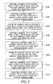
- FIG. 2 shows a flow chart of the operating method for a large dimension plasma enhanced atomic layer deposition cavity of the present invention.
- the method includes inputting a pneumatic valve frequency signal to make a purifying gas enter into the large dimension plasma enhanced atomic layer deposition cavity (S 100 ).
- a pressure signal is outputted to a rotatable throttle valve controller to generate a valve position signal and a rotating frequency signal (S 102 ).
- the rotatable throttle valve is closed and a first gas is filled into the large dimension plasma enhanced atomic layer deposition cavity (S 104 ).
- a pneumatic valve frequency signal is inputted to make a purifying gas enter into the large dimension plasma enhanced atomic layer deposition cavity (S 106 ).
- a pressure signal is outputted to a rotatable throttle valve controller to generate a valve position signal and a rotating frequency signal (S 108 ).
- the rotatable throttle valve is closed and fills a second gas into the large dimension plasma enhanced atomic layer deposition cavity (S 11 O); a pneumatic valve frequency signal is inputted to make a purifying gas enter into the large dimension plasma enhanced atomic layer deposition cavity (S 112 ).
- a pressure signal is outputted to a rotatable throttle valve controller to generate a valve position signal and a rotating frequency signal (S 114 ).
- a rotatable throttle valve is opened via the valve position signal and a rotating frequency signal to exhaust the purifying gas from the large dimension plasma enhanced atomic layer deposition cavity.
- FIG. 3 shows a schematic view of a large dimension plasma enhanced atomic layer deposition cavity of the present invention used for filling gas quickly.
- the large dimension plasma enhanced atomic layer deposition cavity includes an upper electrode plate 40 and a lower electrode plate 42 .
- the lower electrode plate 42 is grounded.
- At least one gas pipe 44 is installed on the upper electrode plate 40 .
- At least one fast gas valve 46 is installed above the gas pipe 44 .
- At least one insulation material 48 is installed under the gas pipe 44 , above the upper electrode plate 40 and around the lower electrode plate 42 to keep the three separated.
- the insulation material 48 can be ceramic, quartz or another material that can be used for insulation.
- the insulation material 48 is spread around the surroundings or the two sides of the lower electrode plate 42 having holes for exhausting the gas.
- FIG. 4 shows a schematic view of the second embodiment of a large dimension plasma enhanced atomic layer deposition cavity of the present invention used for filling gas quickly.
- FIG. 5 shows a schematic view of the second embodiment of a large dimension plasma enhanced atomic layer deposition cavity of the present invention used for filling gas quickly.
- a RF power supply 482 is connected with one side of the upper electrode plate 40 .
- the large dimension plasma enhanced atomic layer deposition cavity has a plurality of gas distributing pipes for the plurality of precursors and the purifying gas.
- the fast valve of each gas-distributing pipe is installed near the cavity so that the plasma enhanced atomic layer deposition apparatus switches the precursors rapidly to increase the deposition rate of the thin film.
- the electrode plate in the manufacturing cavity is installed with gas distributing pipes and each gas distributing pipe has a gas valve that can be opened and closed quickly and is installed before the cavity so that the gas fills the gas distributing pipe to reduce the time needed for transmitting and filling.
- the fast gas valve on the same gas-distributing pipe is operated to introduce the precursor into the manufacturing cavity.
- FIG. 6 shows a schematic view of the first embodiment of the throttle valve of the present invention.
- the present embodiment uses a magnetic force to make the bearing base 62 move linearly.
- the rotatable valve 58 is composed of three blades.
- the blade 56 is used for controlling the cross-section of the pipe to change the gas-flow of the exhaust pipe.
- the other blades 52 and 54 are used for sealing the movement space or opening of the rotatable valve 58 to reduce gas loss. If gas-flow of the exhaust pipe needs to be increased, the rotatable valve 58 is rotated 180 degrees to the side without the valve's blade. In this state, the gas-flow of the exhaust pipe is its largest and co-operates with the rotating frequency to reduce consumption of the precursor and rapidly changes the gas-flow.
- the bearing seal of the rotating machine feedthrough is an O-ring or a Y-ring, or is linked by a magnetic force.
- the linear movement machine feedthrough is implemented by using a step motor 60 to drive a belt, a chain or a rack to change the position of the bearing base via a magnetic force.
- the linear movement machine feedthrough is implemented by a step motor 60 driving a screw rod 64 to change the position of the bearing base of the rotatable valve 56 , and is sealed with a ripple pipe (as shown in FIG. 7 ). The above operation is cooperated with the frequency of the valve operations of the chemical precursor and the purifying gas.
- FIG. 8 shows a schematic view of the third embodiment of the throttle valve of the present invention.
- the present embodiment uses a rotating disk 72 with a hole 70 for rotating.
- the hole 72 of the rotating disk 72 is used for controlling the cross-section of the pipe.
- the exhaust pipe is fully open.
- the hole 72 of the rotating disk 72 is rotated to its other position, the exhaust pipe is completely closed.
- the opening and closing frequency of the exhaust pipe's gas-flow is changed by the rotating speed of the rotating disk 72 .
- the rotating disk 72 is driven by the servomotor 60 and controls the position of the hole 70 . This method is suitable for the large dimension plasma enhanced atomic layer deposition cavity 10 .
- the rotating valve can only control the exhaust pipe when it is open or closed and fine-tuning the gas-flow in the exhaust pipe is not easy. Therefore, the pressure in the manufacturing cavity is controlled by controlling the quantity of gas entering into the cavity via the gas-transmitting pipe. If the opening time for the fast valve of the gas-transmitting pipe is fixed, the pressure in the gas-transmitting pipe is adjusted according to the pressure in the cavity (as shown in FIG. 9 ). When there is not enough pressure in the cavity, the signal generator 30 feeds back an adjusting valve position signal 39 to an adjusting pressure valve of the gas-transmitting pipe to increase the pressure in the pipe.
- FIG. 10 is a schematic view of the control signals in the third embodiment of the throttle valve of the present invention.
- FIG. 11A is a schematic view of the rotatable disk with a signal hole in the third embodiment of the throttle valve of the present invention.
- FIG. 11B is a schematic view of the rotatable disk with two holes in the third embodiment of the throttle valve of the present invention.
- FIG. 11 C is a schematic view of the rotatable disk with a signal non-circular hole in the third embodiment of the throttle valve of the present invention.
- the rotatable disk 72 includes at least one hole 70 .
- the volume of the manufacturing cavity is reduced to a minimum volume. Because the dimension of the substrate is fixed and cannot be reduced, the volume of the manufacturing cavity can be reduced by changing the manufacturing cavity's height.
- the top of the cavity is flat and close to the substrate, the narrow and small space is not suitable for transporting the substrate via a robot's arm.
- the transporting method is modified.
- the substrate is transported via a floating force, as shown in FIG. 12 .
- each air hole on the platform emits nitrogen gas to lift the substrate a little; in other words it acts the same as an air cushion. Therefore, the substrate can be moved by a robot's arm or a piston to push the substrate to the desired location.
Abstract
Description
Claims (6)
Applications Claiming Priority (3)
| Application Number | Priority Date | Filing Date | Title |
|---|---|---|---|
| TW094125879A TWI261313B (en) | 2005-07-29 | 2005-07-29 | A method for a large dimension plasma enhanced atomic layer deposition cavity and an apparatus thereof |
| TW94125879A | 2005-07-29 | ||
| TW94125879 | 2005-07-29 |
Publications (2)
| Publication Number | Publication Date |
|---|---|
| US20070026162A1 US20070026162A1 (en) | 2007-02-01 |
| US8097083B2 true US8097083B2 (en) | 2012-01-17 |
Family
ID=37694654
Family Applications (1)
| Application Number | Title | Priority Date | Filing Date |
|---|---|---|---|
| US11/244,040 Active 2029-01-30 US8097083B2 (en) | 2005-07-29 | 2005-10-06 | Operating method for a large dimension plasma enhanced atomic layer deposition cavity and an apparatus thereof |
Country Status (2)
| Country | Link |
|---|---|
| US (1) | US8097083B2 (en) |
| TW (1) | TWI261313B (en) |
Families Citing this family (256)
| Publication number | Priority date | Publication date | Assignee | Title |
|---|---|---|---|---|
| JP4430718B2 (en) * | 2008-03-21 | 2010-03-10 | 三井造船株式会社 | Atomic layer deposition system |
| US9394608B2 (en) | 2009-04-06 | 2016-07-19 | Asm America, Inc. | Semiconductor processing reactor and components thereof |
| US8802201B2 (en) | 2009-08-14 | 2014-08-12 | Asm America, Inc. | Systems and methods for thin-film deposition of metal oxides using excited nitrogen-oxygen species |
| US20120058576A1 (en) * | 2010-09-03 | 2012-03-08 | Beck Markus E | Deposition System |
| US9312155B2 (en) | 2011-06-06 | 2016-04-12 | Asm Japan K.K. | High-throughput semiconductor-processing apparatus equipped with multiple dual-chamber modules |
| US10854498B2 (en) | 2011-07-15 | 2020-12-01 | Asm Ip Holding B.V. | Wafer-supporting device and method for producing same |
| US20130023129A1 (en) | 2011-07-20 | 2013-01-24 | Asm America, Inc. | Pressure transmitter for a semiconductor processing environment |
| US9017481B1 (en) | 2011-10-28 | 2015-04-28 | Asm America, Inc. | Process feed management for semiconductor substrate processing |
| US20130203259A1 (en) * | 2012-02-07 | 2013-08-08 | Lam Research Corporation | Pressure control valve assembly of plasma processing chamber and rapid alternating process |
| US10714315B2 (en) | 2012-10-12 | 2020-07-14 | Asm Ip Holdings B.V. | Semiconductor reaction chamber showerhead |
| US20150047785A1 (en) * | 2013-08-13 | 2015-02-19 | Lam Research Corporation | Plasma Processing Devices Having Multi-Port Valve Assemblies |
| US10683571B2 (en) | 2014-02-25 | 2020-06-16 | Asm Ip Holding B.V. | Gas supply manifold and method of supplying gases to chamber using same |
| US10167557B2 (en) | 2014-03-18 | 2019-01-01 | Asm Ip Holding B.V. | Gas distribution system, reactor including the system, and methods of using the same |
| US11015245B2 (en) | 2014-03-19 | 2021-05-25 | Asm Ip Holding B.V. | Gas-phase reactor and system having exhaust plenum and components thereof |
| US10858737B2 (en) | 2014-07-28 | 2020-12-08 | Asm Ip Holding B.V. | Showerhead assembly and components thereof |
| US9890456B2 (en) | 2014-08-21 | 2018-02-13 | Asm Ip Holding B.V. | Method and system for in situ formation of gas-phase compounds |
| US10941490B2 (en) | 2014-10-07 | 2021-03-09 | Asm Ip Holding B.V. | Multiple temperature range susceptor, assembly, reactor and system including the susceptor, and methods of using the same |
| US9657845B2 (en) | 2014-10-07 | 2017-05-23 | Asm Ip Holding B.V. | Variable conductance gas distribution apparatus and method |
| US10276355B2 (en) | 2015-03-12 | 2019-04-30 | Asm Ip Holding B.V. | Multi-zone reactor, system including the reactor, and method of using the same |
| US10458018B2 (en) | 2015-06-26 | 2019-10-29 | Asm Ip Holding B.V. | Structures including metal carbide material, devices including the structures, and methods of forming same |
| US10600673B2 (en) | 2015-07-07 | 2020-03-24 | Asm Ip Holding B.V. | Magnetic susceptor to baseplate seal |
| US10211308B2 (en) | 2015-10-21 | 2019-02-19 | Asm Ip Holding B.V. | NbMC layers |
| US11139308B2 (en) | 2015-12-29 | 2021-10-05 | Asm Ip Holding B.V. | Atomic layer deposition of III-V compounds to form V-NAND devices |
| US10529554B2 (en) | 2016-02-19 | 2020-01-07 | Asm Ip Holding B.V. | Method for forming silicon nitride film selectively on sidewalls or flat surfaces of trenches |
| US10190213B2 (en) | 2016-04-21 | 2019-01-29 | Asm Ip Holding B.V. | Deposition of metal borides |
| US10865475B2 (en) | 2016-04-21 | 2020-12-15 | Asm Ip Holding B.V. | Deposition of metal borides and silicides |
| US10032628B2 (en) | 2016-05-02 | 2018-07-24 | Asm Ip Holding B.V. | Source/drain performance through conformal solid state doping |
| US10367080B2 (en) | 2016-05-02 | 2019-07-30 | Asm Ip Holding B.V. | Method of forming a germanium oxynitride film |
| US11453943B2 (en) | 2016-05-25 | 2022-09-27 | Asm Ip Holding B.V. | Method for forming carbon-containing silicon/metal oxide or nitride film by ALD using silicon precursor and hydrocarbon precursor |
| US9859151B1 (en) | 2016-07-08 | 2018-01-02 | Asm Ip Holding B.V. | Selective film deposition method to form air gaps |
| US10612137B2 (en) | 2016-07-08 | 2020-04-07 | Asm Ip Holdings B.V. | Organic reactants for atomic layer deposition |
| US10714385B2 (en) | 2016-07-19 | 2020-07-14 | Asm Ip Holding B.V. | Selective deposition of tungsten |
| KR102532607B1 (en) | 2016-07-28 | 2023-05-15 | 에이에스엠 아이피 홀딩 비.브이. | Substrate processing apparatus and method of operating the same |
| US9812320B1 (en) | 2016-07-28 | 2017-11-07 | Asm Ip Holding B.V. | Method and apparatus for filling a gap |
| US9887082B1 (en) | 2016-07-28 | 2018-02-06 | Asm Ip Holding B.V. | Method and apparatus for filling a gap |
| US10643826B2 (en) | 2016-10-26 | 2020-05-05 | Asm Ip Holdings B.V. | Methods for thermally calibrating reaction chambers |
| US11532757B2 (en) | 2016-10-27 | 2022-12-20 | Asm Ip Holding B.V. | Deposition of charge trapping layers |
| US10229833B2 (en) | 2016-11-01 | 2019-03-12 | Asm Ip Holding B.V. | Methods for forming a transition metal nitride film on a substrate by atomic layer deposition and related semiconductor device structures |
| US10643904B2 (en) | 2016-11-01 | 2020-05-05 | Asm Ip Holdings B.V. | Methods for forming a semiconductor device and related semiconductor device structures |
| US10714350B2 (en) | 2016-11-01 | 2020-07-14 | ASM IP Holdings, B.V. | Methods for forming a transition metal niobium nitride film on a substrate by atomic layer deposition and related semiconductor device structures |
| US10134757B2 (en) | 2016-11-07 | 2018-11-20 | Asm Ip Holding B.V. | Method of processing a substrate and a device manufactured by using the method |
| KR102546317B1 (en) | 2016-11-15 | 2023-06-21 | 에이에스엠 아이피 홀딩 비.브이. | Gas supply unit and substrate processing apparatus including the same |
| TWI608119B (en) * | 2016-11-16 | 2017-12-11 | 矽碁科技股份有限公司 | Atomic layer deposition equipment and pumping speed controlling method therefor |
| KR20180068582A (en) | 2016-12-14 | 2018-06-22 | 에이에스엠 아이피 홀딩 비.브이. | Substrate processing apparatus |
| US11447861B2 (en) | 2016-12-15 | 2022-09-20 | Asm Ip Holding B.V. | Sequential infiltration synthesis apparatus and a method of forming a patterned structure |
| US11581186B2 (en) | 2016-12-15 | 2023-02-14 | Asm Ip Holding B.V. | Sequential infiltration synthesis apparatus |
| KR20180070971A (en) | 2016-12-19 | 2018-06-27 | 에이에스엠 아이피 홀딩 비.브이. | Substrate processing apparatus |
| US10269558B2 (en) | 2016-12-22 | 2019-04-23 | Asm Ip Holding B.V. | Method of forming a structure on a substrate |
| US10867788B2 (en) | 2016-12-28 | 2020-12-15 | Asm Ip Holding B.V. | Method of forming a structure on a substrate |
| US11390950B2 (en) | 2017-01-10 | 2022-07-19 | Asm Ip Holding B.V. | Reactor system and method to reduce residue buildup during a film deposition process |
| US10655221B2 (en) | 2017-02-09 | 2020-05-19 | Asm Ip Holding B.V. | Method for depositing oxide film by thermal ALD and PEALD |
| US10468261B2 (en) | 2017-02-15 | 2019-11-05 | Asm Ip Holding B.V. | Methods for forming a metallic film on a substrate by cyclical deposition and related semiconductor device structures |
| JP6749268B2 (en) * | 2017-03-07 | 2020-09-02 | 東京エレクトロン株式会社 | Substrate processing equipment |
| US10529563B2 (en) | 2017-03-29 | 2020-01-07 | Asm Ip Holdings B.V. | Method for forming doped metal oxide films on a substrate by cyclical deposition and related semiconductor device structures |
| USD876504S1 (en) | 2017-04-03 | 2020-02-25 | Asm Ip Holding B.V. | Exhaust flow control ring for semiconductor deposition apparatus |
| KR102457289B1 (en) | 2017-04-25 | 2022-10-21 | 에이에스엠 아이피 홀딩 비.브이. | Method for depositing a thin film and manufacturing a semiconductor device |
| US10892156B2 (en) | 2017-05-08 | 2021-01-12 | Asm Ip Holding B.V. | Methods for forming a silicon nitride film on a substrate and related semiconductor device structures |
| US10770286B2 (en) | 2017-05-08 | 2020-09-08 | Asm Ip Holdings B.V. | Methods for selectively forming a silicon nitride film on a substrate and related semiconductor device structures |
| US11306395B2 (en) | 2017-06-28 | 2022-04-19 | Asm Ip Holding B.V. | Methods for depositing a transition metal nitride film on a substrate by atomic layer deposition and related deposition apparatus |
| US10685834B2 (en) | 2017-07-05 | 2020-06-16 | Asm Ip Holdings B.V. | Methods for forming a silicon germanium tin layer and related semiconductor device structures |
| KR20190009245A (en) | 2017-07-18 | 2019-01-28 | 에이에스엠 아이피 홀딩 비.브이. | Methods for forming a semiconductor device structure and related semiconductor device structures |
| US10541333B2 (en) | 2017-07-19 | 2020-01-21 | Asm Ip Holding B.V. | Method for depositing a group IV semiconductor and related semiconductor device structures |
| US11374112B2 (en) | 2017-07-19 | 2022-06-28 | Asm Ip Holding B.V. | Method for depositing a group IV semiconductor and related semiconductor device structures |
| US11018002B2 (en) | 2017-07-19 | 2021-05-25 | Asm Ip Holding B.V. | Method for selectively depositing a Group IV semiconductor and related semiconductor device structures |
| US10590535B2 (en) | 2017-07-26 | 2020-03-17 | Asm Ip Holdings B.V. | Chemical treatment, deposition and/or infiltration apparatus and method for using the same |
| US10692741B2 (en) | 2017-08-08 | 2020-06-23 | Asm Ip Holdings B.V. | Radiation shield |
| US10770336B2 (en) | 2017-08-08 | 2020-09-08 | Asm Ip Holding B.V. | Substrate lift mechanism and reactor including same |
| US10249524B2 (en) | 2017-08-09 | 2019-04-02 | Asm Ip Holding B.V. | Cassette holder assembly for a substrate cassette and holding member for use in such assembly |
| US11769682B2 (en) | 2017-08-09 | 2023-09-26 | Asm Ip Holding B.V. | Storage apparatus for storing cassettes for substrates and processing apparatus equipped therewith |
| US11139191B2 (en) | 2017-08-09 | 2021-10-05 | Asm Ip Holding B.V. | Storage apparatus for storing cassettes for substrates and processing apparatus equipped therewith |
| USD900036S1 (en) | 2017-08-24 | 2020-10-27 | Asm Ip Holding B.V. | Heater electrical connector and adapter |
| US11830730B2 (en) | 2017-08-29 | 2023-11-28 | Asm Ip Holding B.V. | Layer forming method and apparatus |
| US11295980B2 (en) | 2017-08-30 | 2022-04-05 | Asm Ip Holding B.V. | Methods for depositing a molybdenum metal film over a dielectric surface of a substrate by a cyclical deposition process and related semiconductor device structures |
| US11056344B2 (en) | 2017-08-30 | 2021-07-06 | Asm Ip Holding B.V. | Layer forming method |
| KR102491945B1 (en) | 2017-08-30 | 2023-01-26 | 에이에스엠 아이피 홀딩 비.브이. | Substrate processing apparatus |
| KR102630301B1 (en) | 2017-09-21 | 2024-01-29 | 에이에스엠 아이피 홀딩 비.브이. | Method of sequential infiltration synthesis treatment of infiltrateable material and structures and devices formed using same |
| US10844484B2 (en) | 2017-09-22 | 2020-11-24 | Asm Ip Holding B.V. | Apparatus for dispensing a vapor phase reactant to a reaction chamber and related methods |
| US10658205B2 (en) | 2017-09-28 | 2020-05-19 | Asm Ip Holdings B.V. | Chemical dispensing apparatus and methods for dispensing a chemical to a reaction chamber |
| US10403504B2 (en) | 2017-10-05 | 2019-09-03 | Asm Ip Holding B.V. | Method for selectively depositing a metallic film on a substrate |
| US10319588B2 (en) | 2017-10-10 | 2019-06-11 | Asm Ip Holding B.V. | Method for depositing a metal chalcogenide on a substrate by cyclical deposition |
| US10923344B2 (en) | 2017-10-30 | 2021-02-16 | Asm Ip Holding B.V. | Methods for forming a semiconductor structure and related semiconductor structures |
| US10910262B2 (en) | 2017-11-16 | 2021-02-02 | Asm Ip Holding B.V. | Method of selectively depositing a capping layer structure on a semiconductor device structure |
| KR102443047B1 (en) | 2017-11-16 | 2022-09-14 | 에이에스엠 아이피 홀딩 비.브이. | Method of processing a substrate and a device manufactured by the same |
| US11022879B2 (en) | 2017-11-24 | 2021-06-01 | Asm Ip Holding B.V. | Method of forming an enhanced unexposed photoresist layer |
| JP7214724B2 (en) | 2017-11-27 | 2023-01-30 | エーエスエム アイピー ホールディング ビー.ブイ. | Storage device for storing wafer cassettes used in batch furnaces |
| TWI791689B (en) | 2017-11-27 | 2023-02-11 | 荷蘭商Asm智慧財產控股私人有限公司 | Apparatus including a clean mini environment |
| US10872771B2 (en) | 2018-01-16 | 2020-12-22 | Asm Ip Holding B. V. | Method for depositing a material film on a substrate within a reaction chamber by a cyclical deposition process and related device structures |
| TWI799494B (en) | 2018-01-19 | 2023-04-21 | 荷蘭商Asm 智慧財產控股公司 | Deposition method |
| WO2019142055A2 (en) | 2018-01-19 | 2019-07-25 | Asm Ip Holding B.V. | Method for depositing a gap-fill layer by plasma-assisted deposition |
| USD903477S1 (en) | 2018-01-24 | 2020-12-01 | Asm Ip Holdings B.V. | Metal clamp |
| US11018047B2 (en) | 2018-01-25 | 2021-05-25 | Asm Ip Holding B.V. | Hybrid lift pin |
| USD880437S1 (en) | 2018-02-01 | 2020-04-07 | Asm Ip Holding B.V. | Gas supply plate for semiconductor manufacturing apparatus |
| US11081345B2 (en) | 2018-02-06 | 2021-08-03 | Asm Ip Holding B.V. | Method of post-deposition treatment for silicon oxide film |
| US10896820B2 (en) | 2018-02-14 | 2021-01-19 | Asm Ip Holding B.V. | Method for depositing a ruthenium-containing film on a substrate by a cyclical deposition process |
| US11685991B2 (en) | 2018-02-14 | 2023-06-27 | Asm Ip Holding B.V. | Method for depositing a ruthenium-containing film on a substrate by a cyclical deposition process |
| US10731249B2 (en) | 2018-02-15 | 2020-08-04 | Asm Ip Holding B.V. | Method of forming a transition metal containing film on a substrate by a cyclical deposition process, a method for supplying a transition metal halide compound to a reaction chamber, and related vapor deposition apparatus |
| US10658181B2 (en) | 2018-02-20 | 2020-05-19 | Asm Ip Holding B.V. | Method of spacer-defined direct patterning in semiconductor fabrication |
| KR102636427B1 (en) | 2018-02-20 | 2024-02-13 | 에이에스엠 아이피 홀딩 비.브이. | Substrate processing method and apparatus |
| US10975470B2 (en) | 2018-02-23 | 2021-04-13 | Asm Ip Holding B.V. | Apparatus for detecting or monitoring for a chemical precursor in a high temperature environment |
| US11473195B2 (en) | 2018-03-01 | 2022-10-18 | Asm Ip Holding B.V. | Semiconductor processing apparatus and a method for processing a substrate |
| US11629406B2 (en) | 2018-03-09 | 2023-04-18 | Asm Ip Holding B.V. | Semiconductor processing apparatus comprising one or more pyrometers for measuring a temperature of a substrate during transfer of the substrate |
| US11114283B2 (en) | 2018-03-16 | 2021-09-07 | Asm Ip Holding B.V. | Reactor, system including the reactor, and methods of manufacturing and using same |
| KR102646467B1 (en) | 2018-03-27 | 2024-03-11 | 에이에스엠 아이피 홀딩 비.브이. | Method of forming an electrode on a substrate and a semiconductor device structure including an electrode |
| US11230766B2 (en) | 2018-03-29 | 2022-01-25 | Asm Ip Holding B.V. | Substrate processing apparatus and method |
| US11088002B2 (en) | 2018-03-29 | 2021-08-10 | Asm Ip Holding B.V. | Substrate rack and a substrate processing system and method |
| KR102501472B1 (en) | 2018-03-30 | 2023-02-20 | 에이에스엠 아이피 홀딩 비.브이. | Substrate processing method |
| TWI811348B (en) | 2018-05-08 | 2023-08-11 | 荷蘭商Asm 智慧財產控股公司 | Methods for depositing an oxide film on a substrate by a cyclical deposition process and related device structures |
| KR20190129718A (en) | 2018-05-11 | 2019-11-20 | 에이에스엠 아이피 홀딩 비.브이. | Methods for forming a doped metal carbide film on a substrate and related semiconductor device structures |
| KR102596988B1 (en) | 2018-05-28 | 2023-10-31 | 에이에스엠 아이피 홀딩 비.브이. | Method of processing a substrate and a device manufactured by the same |
| US11718913B2 (en) | 2018-06-04 | 2023-08-08 | Asm Ip Holding B.V. | Gas distribution system and reactor system including same |
| TW202013553A (en) | 2018-06-04 | 2020-04-01 | 荷蘭商Asm 智慧財產控股公司 | Wafer handling chamber with moisture reduction |
| US11286562B2 (en) | 2018-06-08 | 2022-03-29 | Asm Ip Holding B.V. | Gas-phase chemical reactor and method of using same |
| KR102568797B1 (en) | 2018-06-21 | 2023-08-21 | 에이에스엠 아이피 홀딩 비.브이. | Substrate processing system |
| US10797133B2 (en) | 2018-06-21 | 2020-10-06 | Asm Ip Holding B.V. | Method for depositing a phosphorus doped silicon arsenide film and related semiconductor device structures |
| CN112292478A (en) | 2018-06-27 | 2021-01-29 | Asm Ip私人控股有限公司 | Cyclic deposition methods for forming metal-containing materials and films and structures containing metal-containing materials |
| JP2021529880A (en) | 2018-06-27 | 2021-11-04 | エーエスエム・アイピー・ホールディング・ベー・フェー | Periodic deposition methods for forming metal-containing materials and films and structures containing metal-containing materials |
| KR20200002519A (en) | 2018-06-29 | 2020-01-08 | 에이에스엠 아이피 홀딩 비.브이. | Method for depositing a thin film and manufacturing a semiconductor device |
| US10612136B2 (en) | 2018-06-29 | 2020-04-07 | ASM IP Holding, B.V. | Temperature-controlled flange and reactor system including same |
| US10755922B2 (en) | 2018-07-03 | 2020-08-25 | Asm Ip Holding B.V. | Method for depositing silicon-free carbon-containing film as gap-fill layer by pulse plasma-assisted deposition |
| US10388513B1 (en) | 2018-07-03 | 2019-08-20 | Asm Ip Holding B.V. | Method for depositing silicon-free carbon-containing film as gap-fill layer by pulse plasma-assisted deposition |
| US10767789B2 (en) | 2018-07-16 | 2020-09-08 | Asm Ip Holding B.V. | Diaphragm valves, valve components, and methods for forming valve components |
| US11053591B2 (en) | 2018-08-06 | 2021-07-06 | Asm Ip Holding B.V. | Multi-port gas injection system and reactor system including same |
| US10883175B2 (en) | 2018-08-09 | 2021-01-05 | Asm Ip Holding B.V. | Vertical furnace for processing substrates and a liner for use therein |
| US10829852B2 (en) | 2018-08-16 | 2020-11-10 | Asm Ip Holding B.V. | Gas distribution device for a wafer processing apparatus |
| US11430674B2 (en) | 2018-08-22 | 2022-08-30 | Asm Ip Holding B.V. | Sensor array, apparatus for dispensing a vapor phase reactant to a reaction chamber and related methods |
| US11024523B2 (en) | 2018-09-11 | 2021-06-01 | Asm Ip Holding B.V. | Substrate processing apparatus and method |
| KR20200030162A (en) | 2018-09-11 | 2020-03-20 | 에이에스엠 아이피 홀딩 비.브이. | Method for deposition of a thin film |
| US11049751B2 (en) | 2018-09-14 | 2021-06-29 | Asm Ip Holding B.V. | Cassette supply system to store and handle cassettes and processing apparatus equipped therewith |
| CN110970344A (en) | 2018-10-01 | 2020-04-07 | Asm Ip控股有限公司 | Substrate holding apparatus, system including the same, and method of using the same |
| US11232963B2 (en) | 2018-10-03 | 2022-01-25 | Asm Ip Holding B.V. | Substrate processing apparatus and method |
| KR102592699B1 (en) | 2018-10-08 | 2023-10-23 | 에이에스엠 아이피 홀딩 비.브이. | Substrate support unit and apparatuses for depositing thin film and processing the substrate including the same |
| US10847365B2 (en) | 2018-10-11 | 2020-11-24 | Asm Ip Holding B.V. | Method of forming conformal silicon carbide film by cyclic CVD |
| US10811256B2 (en) | 2018-10-16 | 2020-10-20 | Asm Ip Holding B.V. | Method for etching a carbon-containing feature |
| KR102605121B1 (en) | 2018-10-19 | 2023-11-23 | 에이에스엠 아이피 홀딩 비.브이. | Substrate processing apparatus and substrate processing method |
| KR102546322B1 (en) | 2018-10-19 | 2023-06-21 | 에이에스엠 아이피 홀딩 비.브이. | Substrate processing apparatus and substrate processing method |
| USD948463S1 (en) | 2018-10-24 | 2022-04-12 | Asm Ip Holding B.V. | Susceptor for semiconductor substrate supporting apparatus |
| US11087997B2 (en) | 2018-10-31 | 2021-08-10 | Asm Ip Holding B.V. | Substrate processing apparatus for processing substrates |
| KR20200051105A (en) | 2018-11-02 | 2020-05-13 | 에이에스엠 아이피 홀딩 비.브이. | Substrate support unit and substrate processing apparatus including the same |
| US11572620B2 (en) | 2018-11-06 | 2023-02-07 | Asm Ip Holding B.V. | Methods for selectively depositing an amorphous silicon film on a substrate |
| US11031242B2 (en) | 2018-11-07 | 2021-06-08 | Asm Ip Holding B.V. | Methods for depositing a boron doped silicon germanium film |
| US10818758B2 (en) | 2018-11-16 | 2020-10-27 | Asm Ip Holding B.V. | Methods for forming a metal silicate film on a substrate in a reaction chamber and related semiconductor device structures |
| US10847366B2 (en) | 2018-11-16 | 2020-11-24 | Asm Ip Holding B.V. | Methods for depositing a transition metal chalcogenide film on a substrate by a cyclical deposition process |
| US10559458B1 (en) | 2018-11-26 | 2020-02-11 | Asm Ip Holding B.V. | Method of forming oxynitride film |
| US11217444B2 (en) | 2018-11-30 | 2022-01-04 | Asm Ip Holding B.V. | Method for forming an ultraviolet radiation responsive metal oxide-containing film |
| KR102636428B1 (en) | 2018-12-04 | 2024-02-13 | 에이에스엠 아이피 홀딩 비.브이. | A method for cleaning a substrate processing apparatus |
| US11158513B2 (en) | 2018-12-13 | 2021-10-26 | Asm Ip Holding B.V. | Methods for forming a rhenium-containing film on a substrate by a cyclical deposition process and related semiconductor device structures |
| TW202037745A (en) | 2018-12-14 | 2020-10-16 | 荷蘭商Asm Ip私人控股有限公司 | Method of forming device structure, structure formed by the method and system for performing the method |
| TWI819180B (en) | 2019-01-17 | 2023-10-21 | 荷蘭商Asm 智慧財產控股公司 | Methods of forming a transition metal containing film on a substrate by a cyclical deposition process |
| KR20200091543A (en) | 2019-01-22 | 2020-07-31 | 에이에스엠 아이피 홀딩 비.브이. | Semiconductor processing device |
| CN111524788B (en) | 2019-02-01 | 2023-11-24 | Asm Ip私人控股有限公司 | Method for topologically selective film formation of silicon oxide |
| KR102626263B1 (en) | 2019-02-20 | 2024-01-16 | 에이에스엠 아이피 홀딩 비.브이. | Cyclical deposition method including treatment step and apparatus for same |
| JP2020136677A (en) | 2019-02-20 | 2020-08-31 | エーエスエム・アイピー・ホールディング・ベー・フェー | Periodic accumulation method for filing concave part formed inside front surface of base material, and device |
| KR20200102357A (en) | 2019-02-20 | 2020-08-31 | 에이에스엠 아이피 홀딩 비.브이. | Apparatus and methods for plug fill deposition in 3-d nand applications |
| JP2020136678A (en) | 2019-02-20 | 2020-08-31 | エーエスエム・アイピー・ホールディング・ベー・フェー | Method for filing concave part formed inside front surface of base material, and device |
| TW202100794A (en) | 2019-02-22 | 2021-01-01 | 荷蘭商Asm Ip私人控股有限公司 | Substrate processing apparatus and method for processing substrate |
| US11742198B2 (en) | 2019-03-08 | 2023-08-29 | Asm Ip Holding B.V. | Structure including SiOCN layer and method of forming same |
| KR20200108243A (en) | 2019-03-08 | 2020-09-17 | 에이에스엠 아이피 홀딩 비.브이. | Structure Including SiOC Layer and Method of Forming Same |
| KR20200108242A (en) | 2019-03-08 | 2020-09-17 | 에이에스엠 아이피 홀딩 비.브이. | Method for Selective Deposition of Silicon Nitride Layer and Structure Including Selectively-Deposited Silicon Nitride Layer |
| JP2020167398A (en) | 2019-03-28 | 2020-10-08 | エーエスエム・アイピー・ホールディング・ベー・フェー | Door opener and substrate processing apparatus provided therewith |
| KR20200116855A (en) | 2019-04-01 | 2020-10-13 | 에이에스엠 아이피 홀딩 비.브이. | Method of manufacturing semiconductor device |
| US11447864B2 (en) | 2019-04-19 | 2022-09-20 | Asm Ip Holding B.V. | Layer forming method and apparatus |
| KR20200125453A (en) | 2019-04-24 | 2020-11-04 | 에이에스엠 아이피 홀딩 비.브이. | Gas-phase reactor system and method of using same |
| KR20200130118A (en) | 2019-05-07 | 2020-11-18 | 에이에스엠 아이피 홀딩 비.브이. | Method for Reforming Amorphous Carbon Polymer Film |
| KR20200130121A (en) | 2019-05-07 | 2020-11-18 | 에이에스엠 아이피 홀딩 비.브이. | Chemical source vessel with dip tube |
| KR20200130652A (en) | 2019-05-10 | 2020-11-19 | 에이에스엠 아이피 홀딩 비.브이. | Method of depositing material onto a surface and structure formed according to the method |
| JP2020188255A (en) | 2019-05-16 | 2020-11-19 | エーエスエム アイピー ホールディング ビー.ブイ. | Wafer boat handling device, vertical batch furnace, and method |
| USD975665S1 (en) | 2019-05-17 | 2023-01-17 | Asm Ip Holding B.V. | Susceptor shaft |
| USD947913S1 (en) | 2019-05-17 | 2022-04-05 | Asm Ip Holding B.V. | Susceptor shaft |
| USD935572S1 (en) | 2019-05-24 | 2021-11-09 | Asm Ip Holding B.V. | Gas channel plate |
| USD922229S1 (en) | 2019-06-05 | 2021-06-15 | Asm Ip Holding B.V. | Device for controlling a temperature of a gas supply unit |
| KR20200141003A (en) | 2019-06-06 | 2020-12-17 | 에이에스엠 아이피 홀딩 비.브이. | Gas-phase reactor system including a gas detector |
| KR20200143254A (en) | 2019-06-11 | 2020-12-23 | 에이에스엠 아이피 홀딩 비.브이. | Method of forming an electronic structure using an reforming gas, system for performing the method, and structure formed using the method |
| USD944946S1 (en) | 2019-06-14 | 2022-03-01 | Asm Ip Holding B.V. | Shower plate |
| USD931978S1 (en) | 2019-06-27 | 2021-09-28 | Asm Ip Holding B.V. | Showerhead vacuum transport |
| KR20210005515A (en) | 2019-07-03 | 2021-01-14 | 에이에스엠 아이피 홀딩 비.브이. | Temperature control assembly for substrate processing apparatus and method of using same |
| JP2021015791A (en) | 2019-07-09 | 2021-02-12 | エーエスエム アイピー ホールディング ビー.ブイ. | Plasma device and substrate processing method using coaxial waveguide |
| CN112216646A (en) | 2019-07-10 | 2021-01-12 | Asm Ip私人控股有限公司 | Substrate supporting assembly and substrate processing device comprising same |
| KR20210010307A (en) | 2019-07-16 | 2021-01-27 | 에이에스엠 아이피 홀딩 비.브이. | Substrate processing apparatus |
| KR20210010820A (en) | 2019-07-17 | 2021-01-28 | 에이에스엠 아이피 홀딩 비.브이. | Methods of forming silicon germanium structures |
| KR20210010816A (en) | 2019-07-17 | 2021-01-28 | 에이에스엠 아이피 홀딩 비.브이. | Radical assist ignition plasma system and method |
| US11643724B2 (en) | 2019-07-18 | 2023-05-09 | Asm Ip Holding B.V. | Method of forming structures using a neutral beam |
| TW202121506A (en) | 2019-07-19 | 2021-06-01 | 荷蘭商Asm Ip私人控股有限公司 | Method of forming topology-controlled amorphous carbon polymer film |
| TW202113936A (en) | 2019-07-29 | 2021-04-01 | 荷蘭商Asm Ip私人控股有限公司 | Methods for selective deposition utilizing n-type dopants and/or alternative dopants to achieve high dopant incorporation |
| CN112309899A (en) | 2019-07-30 | 2021-02-02 | Asm Ip私人控股有限公司 | Substrate processing apparatus |
| CN112309900A (en) | 2019-07-30 | 2021-02-02 | Asm Ip私人控股有限公司 | Substrate processing apparatus |
| US11587814B2 (en) | 2019-07-31 | 2023-02-21 | Asm Ip Holding B.V. | Vertical batch furnace assembly |
| US11227782B2 (en) | 2019-07-31 | 2022-01-18 | Asm Ip Holding B.V. | Vertical batch furnace assembly |
| US11587815B2 (en) | 2019-07-31 | 2023-02-21 | Asm Ip Holding B.V. | Vertical batch furnace assembly |
| CN112323048B (en) | 2019-08-05 | 2024-02-09 | Asm Ip私人控股有限公司 | Liquid level sensor for chemical source container |
| USD965044S1 (en) | 2019-08-19 | 2022-09-27 | Asm Ip Holding B.V. | Susceptor shaft |
| USD965524S1 (en) | 2019-08-19 | 2022-10-04 | Asm Ip Holding B.V. | Susceptor support |
| JP2021031769A (en) | 2019-08-21 | 2021-03-01 | エーエスエム アイピー ホールディング ビー.ブイ. | Production apparatus of mixed gas of film deposition raw material and film deposition apparatus |
| USD930782S1 (en) | 2019-08-22 | 2021-09-14 | Asm Ip Holding B.V. | Gas distributor |
| USD940837S1 (en) | 2019-08-22 | 2022-01-11 | Asm Ip Holding B.V. | Electrode |
| USD949319S1 (en) | 2019-08-22 | 2022-04-19 | Asm Ip Holding B.V. | Exhaust duct |
| KR20210024423A (en) | 2019-08-22 | 2021-03-05 | 에이에스엠 아이피 홀딩 비.브이. | Method for forming a structure with a hole |
| USD979506S1 (en) | 2019-08-22 | 2023-02-28 | Asm Ip Holding B.V. | Insulator |
| KR20210024420A (en) | 2019-08-23 | 2021-03-05 | 에이에스엠 아이피 홀딩 비.브이. | Method for depositing silicon oxide film having improved quality by peald using bis(diethylamino)silane |
| US11286558B2 (en) | 2019-08-23 | 2022-03-29 | Asm Ip Holding B.V. | Methods for depositing a molybdenum nitride film on a surface of a substrate by a cyclical deposition process and related semiconductor device structures including a molybdenum nitride film |
| KR20210029090A (en) | 2019-09-04 | 2021-03-15 | 에이에스엠 아이피 홀딩 비.브이. | Methods for selective deposition using a sacrificial capping layer |
| KR20210029663A (en) | 2019-09-05 | 2021-03-16 | 에이에스엠 아이피 홀딩 비.브이. | Substrate processing apparatus |
| US11562901B2 (en) | 2019-09-25 | 2023-01-24 | Asm Ip Holding B.V. | Substrate processing method |
| CN112593212B (en) | 2019-10-02 | 2023-12-22 | Asm Ip私人控股有限公司 | Method for forming topologically selective silicon oxide film by cyclic plasma enhanced deposition process |
| TW202129060A (en) | 2019-10-08 | 2021-08-01 | 荷蘭商Asm Ip控股公司 | Substrate processing device, and substrate processing method |
| KR20210043460A (en) | 2019-10-10 | 2021-04-21 | 에이에스엠 아이피 홀딩 비.브이. | Method of forming a photoresist underlayer and structure including same |
| KR20210045930A (en) | 2019-10-16 | 2021-04-27 | 에이에스엠 아이피 홀딩 비.브이. | Method of Topology-Selective Film Formation of Silicon Oxide |
| US11637014B2 (en) | 2019-10-17 | 2023-04-25 | Asm Ip Holding B.V. | Methods for selective deposition of doped semiconductor material |
| KR20210047808A (en) | 2019-10-21 | 2021-04-30 | 에이에스엠 아이피 홀딩 비.브이. | Apparatus and methods for selectively etching films |
| US11646205B2 (en) | 2019-10-29 | 2023-05-09 | Asm Ip Holding B.V. | Methods of selectively forming n-type doped material on a surface, systems for selectively forming n-type doped material, and structures formed using same |
| KR20210054983A (en) | 2019-11-05 | 2021-05-14 | 에이에스엠 아이피 홀딩 비.브이. | Structures with doped semiconductor layers and methods and systems for forming same |
| US11501968B2 (en) | 2019-11-15 | 2022-11-15 | Asm Ip Holding B.V. | Method for providing a semiconductor device with silicon filled gaps |
| KR20210062561A (en) | 2019-11-20 | 2021-05-31 | 에이에스엠 아이피 홀딩 비.브이. | Method of depositing carbon-containing material on a surface of a substrate, structure formed using the method, and system for forming the structure |
| CN112951697A (en) | 2019-11-26 | 2021-06-11 | Asm Ip私人控股有限公司 | Substrate processing apparatus |
| KR20210065848A (en) | 2019-11-26 | 2021-06-04 | 에이에스엠 아이피 홀딩 비.브이. | Methods for selectivley forming a target film on a substrate comprising a first dielectric surface and a second metallic surface |
| CN112885692A (en) | 2019-11-29 | 2021-06-01 | Asm Ip私人控股有限公司 | Substrate processing apparatus |
| CN112885693A (en) | 2019-11-29 | 2021-06-01 | Asm Ip私人控股有限公司 | Substrate processing apparatus |
| JP2021090042A (en) | 2019-12-02 | 2021-06-10 | エーエスエム アイピー ホールディング ビー.ブイ. | Substrate processing apparatus and substrate processing method |
| KR20210070898A (en) | 2019-12-04 | 2021-06-15 | 에이에스엠 아이피 홀딩 비.브이. | Substrate processing apparatus |
| JP2021097227A (en) | 2019-12-17 | 2021-06-24 | エーエスエム・アイピー・ホールディング・ベー・フェー | Method of forming vanadium nitride layer and structure including vanadium nitride layer |
| KR20210080214A (en) | 2019-12-19 | 2021-06-30 | 에이에스엠 아이피 홀딩 비.브이. | Methods for filling a gap feature on a substrate and related semiconductor structures |
| KR20210095050A (en) | 2020-01-20 | 2021-07-30 | 에이에스엠 아이피 홀딩 비.브이. | Method of forming thin film and method of modifying surface of thin film |
| TW202130846A (en) | 2020-02-03 | 2021-08-16 | 荷蘭商Asm Ip私人控股有限公司 | Method of forming structures including a vanadium or indium layer |
| KR20210100010A (en) | 2020-02-04 | 2021-08-13 | 에이에스엠 아이피 홀딩 비.브이. | Method and apparatus for transmittance measurements of large articles |
| US11776846B2 (en) | 2020-02-07 | 2023-10-03 | Asm Ip Holding B.V. | Methods for depositing gap filling fluids and related systems and devices |
| TW202146715A (en) | 2020-02-17 | 2021-12-16 | 荷蘭商Asm Ip私人控股有限公司 | Method for growing phosphorous-doped silicon layer and system of the same |
| KR20210116240A (en) | 2020-03-11 | 2021-09-27 | 에이에스엠 아이피 홀딩 비.브이. | Substrate handling device with adjustable joints |
| US11876356B2 (en) | 2020-03-11 | 2024-01-16 | Asm Ip Holding B.V. | Lockout tagout assembly and system and method of using same |
| KR20210124042A (en) | 2020-04-02 | 2021-10-14 | 에이에스엠 아이피 홀딩 비.브이. | Thin film forming method |
| TW202146689A (en) | 2020-04-03 | 2021-12-16 | 荷蘭商Asm Ip控股公司 | Method for forming barrier layer and method for manufacturing semiconductor device |
| TW202145344A (en) | 2020-04-08 | 2021-12-01 | 荷蘭商Asm Ip私人控股有限公司 | Apparatus and methods for selectively etching silcon oxide films |
| US11821078B2 (en) | 2020-04-15 | 2023-11-21 | Asm Ip Holding B.V. | Method for forming precoat film and method for forming silicon-containing film |
| KR20210132605A (en) | 2020-04-24 | 2021-11-04 | 에이에스엠 아이피 홀딩 비.브이. | Vertical batch furnace assembly comprising a cooling gas supply |
| KR20210132576A (en) | 2020-04-24 | 2021-11-04 | 에이에스엠 아이피 홀딩 비.브이. | Method of forming vanadium nitride-containing layer and structure comprising the same |
| KR20210132600A (en) | 2020-04-24 | 2021-11-04 | 에이에스엠 아이피 홀딩 비.브이. | Methods and systems for depositing a layer comprising vanadium, nitrogen, and a further element |
| KR20210134869A (en) | 2020-05-01 | 2021-11-11 | 에이에스엠 아이피 홀딩 비.브이. | Fast FOUP swapping with a FOUP handler |
| KR20210141379A (en) | 2020-05-13 | 2021-11-23 | 에이에스엠 아이피 홀딩 비.브이. | Laser alignment fixture for a reactor system |
| KR20210143653A (en) | 2020-05-19 | 2021-11-29 | 에이에스엠 아이피 홀딩 비.브이. | Substrate processing apparatus |
| KR20210145078A (en) | 2020-05-21 | 2021-12-01 | 에이에스엠 아이피 홀딩 비.브이. | Structures including multiple carbon layers and methods of forming and using same |
| TW202201602A (en) | 2020-05-29 | 2022-01-01 | 荷蘭商Asm Ip私人控股有限公司 | Substrate processing device |
| TW202218133A (en) | 2020-06-24 | 2022-05-01 | 荷蘭商Asm Ip私人控股有限公司 | Method for forming a layer provided with silicon |
| TW202217953A (en) | 2020-06-30 | 2022-05-01 | 荷蘭商Asm Ip私人控股有限公司 | Substrate processing method |
| TW202219628A (en) | 2020-07-17 | 2022-05-16 | 荷蘭商Asm Ip私人控股有限公司 | Structures and methods for use in photolithography |
| TW202204662A (en) | 2020-07-20 | 2022-02-01 | 荷蘭商Asm Ip私人控股有限公司 | Method and system for depositing molybdenum layers |
| KR20220027026A (en) | 2020-08-26 | 2022-03-07 | 에이에스엠 아이피 홀딩 비.브이. | Method and system for forming metal silicon oxide and metal silicon oxynitride |
| USD990534S1 (en) | 2020-09-11 | 2023-06-27 | Asm Ip Holding B.V. | Weighted lift pin |
| USD1012873S1 (en) | 2020-09-24 | 2024-01-30 | Asm Ip Holding B.V. | Electrode for semiconductor processing apparatus |
| TW202229613A (en) | 2020-10-14 | 2022-08-01 | 荷蘭商Asm Ip私人控股有限公司 | Method of depositing material on stepped structure |
| KR20220053482A (en) | 2020-10-22 | 2022-04-29 | 에이에스엠 아이피 홀딩 비.브이. | Method of depositing vanadium metal, structure, device and a deposition assembly |
| TW202223136A (en) | 2020-10-28 | 2022-06-16 | 荷蘭商Asm Ip私人控股有限公司 | Method for forming layer on substrate, and semiconductor processing system |
| KR20220076343A (en) | 2020-11-30 | 2022-06-08 | 에이에스엠 아이피 홀딩 비.브이. | an injector configured for arrangement within a reaction chamber of a substrate processing apparatus |
| US11946137B2 (en) | 2020-12-16 | 2024-04-02 | Asm Ip Holding B.V. | Runout and wobble measurement fixtures |
| TW202231903A (en) | 2020-12-22 | 2022-08-16 | 荷蘭商Asm Ip私人控股有限公司 | Transition metal deposition method, transition metal layer, and deposition assembly for depositing transition metal on substrate |
| USD981973S1 (en) | 2021-05-11 | 2023-03-28 | Asm Ip Holding B.V. | Reactor wall for substrate processing apparatus |
| USD980814S1 (en) | 2021-05-11 | 2023-03-14 | Asm Ip Holding B.V. | Gas distributor for substrate processing apparatus |
| USD980813S1 (en) | 2021-05-11 | 2023-03-14 | Asm Ip Holding B.V. | Gas flow control plate for substrate processing apparatus |
| USD990441S1 (en) | 2021-09-07 | 2023-06-27 | Asm Ip Holding B.V. | Gas flow control plate |
Citations (11)
| Publication number | Priority date | Publication date | Assignee | Title |
|---|---|---|---|---|
| US5433520A (en) * | 1993-12-13 | 1995-07-18 | Michigan Ash Sales Company | Method and apparatus for continuously processing particulate cementitious material and fly ash solids and mixing them with a liquid to provide a liquid slurry of consistent proportions |
| US5565038A (en) * | 1991-05-16 | 1996-10-15 | Intel Corporation | Interhalogen cleaning of process equipment |
| US6428859B1 (en) | 2000-12-06 | 2002-08-06 | Angstron Systems, Inc. | Sequential method for depositing a film by modulated ion-induced atomic layer deposition (MII-ALD) |
| US20030011022A1 (en) * | 1999-08-31 | 2003-01-16 | Nec Corporation | Semiconductor device and a process for manufacturing a oxide film |
| TW563176B (en) | 2001-10-26 | 2003-11-21 | Applied Materials Inc | Gas delivery apparatus for atomic layer deposition |
| US20040013531A1 (en) * | 2002-05-22 | 2004-01-22 | Applied Materials, Inc. | Variable speed pump control |
| TW578212B (en) | 2001-08-15 | 2004-03-01 | Asm Inc | Atomic layer deposition reactor |
| US20040217311A1 (en) * | 2003-04-29 | 2004-11-04 | Taiwan Semiconductor Manufacturing Co., Ltd. | Fully-sealing throttle valve |
| US20050252563A1 (en) * | 2004-05-11 | 2005-11-17 | Primary Flow Signal, Inc. | Gate valve |
| US20060042754A1 (en) * | 2004-07-30 | 2006-03-02 | Tokyo Electron Limited | Plasma etching apparatus |
| US20060207314A1 (en) * | 2005-03-16 | 2006-09-21 | Tokyo Electron Limited | Vacuum apparatus, method for measuring a leak rate thereof, program used in measuring the leak rate and storage medium storing the program |
-
2005
- 2005-07-29 TW TW094125879A patent/TWI261313B/en active
- 2005-10-06 US US11/244,040 patent/US8097083B2/en active Active
Patent Citations (11)
| Publication number | Priority date | Publication date | Assignee | Title |
|---|---|---|---|---|
| US5565038A (en) * | 1991-05-16 | 1996-10-15 | Intel Corporation | Interhalogen cleaning of process equipment |
| US5433520A (en) * | 1993-12-13 | 1995-07-18 | Michigan Ash Sales Company | Method and apparatus for continuously processing particulate cementitious material and fly ash solids and mixing them with a liquid to provide a liquid slurry of consistent proportions |
| US20030011022A1 (en) * | 1999-08-31 | 2003-01-16 | Nec Corporation | Semiconductor device and a process for manufacturing a oxide film |
| US6428859B1 (en) | 2000-12-06 | 2002-08-06 | Angstron Systems, Inc. | Sequential method for depositing a film by modulated ion-induced atomic layer deposition (MII-ALD) |
| TW578212B (en) | 2001-08-15 | 2004-03-01 | Asm Inc | Atomic layer deposition reactor |
| TW563176B (en) | 2001-10-26 | 2003-11-21 | Applied Materials Inc | Gas delivery apparatus for atomic layer deposition |
| US20040013531A1 (en) * | 2002-05-22 | 2004-01-22 | Applied Materials, Inc. | Variable speed pump control |
| US20040217311A1 (en) * | 2003-04-29 | 2004-11-04 | Taiwan Semiconductor Manufacturing Co., Ltd. | Fully-sealing throttle valve |
| US20050252563A1 (en) * | 2004-05-11 | 2005-11-17 | Primary Flow Signal, Inc. | Gate valve |
| US20060042754A1 (en) * | 2004-07-30 | 2006-03-02 | Tokyo Electron Limited | Plasma etching apparatus |
| US20060207314A1 (en) * | 2005-03-16 | 2006-09-21 | Tokyo Electron Limited | Vacuum apparatus, method for measuring a leak rate thereof, program used in measuring the leak rate and storage medium storing the program |
Also Published As
| Publication number | Publication date |
|---|---|
| US20070026162A1 (en) | 2007-02-01 |
| TWI261313B (en) | 2006-09-01 |
| TW200705550A (en) | 2007-02-01 |
Similar Documents
| Publication | Publication Date | Title |
|---|---|---|
| US8097083B2 (en) | Operating method for a large dimension plasma enhanced atomic layer deposition cavity and an apparatus thereof | |
| CN101322224B (en) | Processing device | |
| CN101713067B (en) | Film formation method and film formation apparatus | |
| TW201834008A (en) | Method for high modulus ald sio2 spacer | |
| US20110212625A1 (en) | Substrate processing apparatus and method of manufacturing semiconductor device | |
| CN101688296A (en) | Vacuum processing system and substrate transfer method | |
| US20070007128A1 (en) | Silicon film forming apparatus | |
| JP2017504725A (en) | Atomic layer deposition processing chamber allowing low pressure tool change | |
| KR20030062365A (en) | Thin film forming method and thin film forming device | |
| JP2004204339A (en) | Apparatus and method for treatment | |
| US7582571B2 (en) | Substrate processing method and recording medium | |
| JP5255806B2 (en) | Film forming apparatus control method, film forming method, and film forming apparatus | |
| WO2013134151A1 (en) | Split pumping method, apparatus, and system | |
| US20100259162A1 (en) | Film forming device control method, film forming method, film forming device, organic el electronic device, and recording medium storing its control program | |
| WO2022097539A1 (en) | Substrate processing method and substrate processing device | |
| CN101215692B (en) | Multiple reaction cavity atom layer deposition device and method | |
| TW201312631A (en) | Method and apparatus for gas distribution and plasma application in a linear deposition chamber | |
| KR20110102330A (en) | Film-forming method, film-forming apparatus and storage medium | |
| KR102349330B1 (en) | Thin film encapsulation processing system and process kit | |
| KR101168150B1 (en) | Thin layer deposition apparatus | |
| US20220178029A1 (en) | Deposition apparatus and deposition method | |
| JP2011171468A (en) | Thin film formation device and method for forming the thin film | |
| KR101526861B1 (en) | Gas supply unit and thin film deposition apparatus having the same | |
| US20230340663A1 (en) | Plasma-enhanced method and system for forming a silicon oxycarbide layer and structure formed using sameplasma-enhanced method and system for forming a silicon oxycarbide layer and structure formed using same | |
| US11538678B2 (en) | Deposition method |
Legal Events
| Date | Code | Title | Description |
|---|---|---|---|
| AS | Assignment |
Owner name: INDUSTRIAL TECHNOLOGY RESEARCH INSTITUTE, TAIWAN Free format text: ASSIGNMENT OF ASSIGNORS INTEREST;ASSIGNORS:WEI, HUNG-WEN;TING, HUNG-CHE;REEL/FRAME:017070/0357 Effective date: 20050909 |
|
| AS | Assignment |
Owner name: ABOMEM TECHNOLOGY CORPORATION, TAIWAN Free format text: ASSIGNMENT OF ASSIGNORS INTEREST;ASSIGNOR:INDUSTRIAL TECHNOLOGY RESEARCH INSTITUTE;REEL/FRAME:026339/0979 Effective date: 20110302 |
|
| AS | Assignment |
Owner name: CHINA STAR OPTOELECTRONICS INTERNATIONAL (HK) LIMI Free format text: ASSIGNMENT OF ASSIGNORS INTEREST;ASSIGNOR:ABOMEM TECHNOLOGY CORPORATION;REEL/FRAME:026365/0150 Effective date: 20110505 |
|
| STCF | Information on status: patent grant |
Free format text: PATENTED CASE |
|
| FEPP | Fee payment procedure |
Free format text: PAYOR NUMBER ASSIGNED (ORIGINAL EVENT CODE: ASPN); ENTITY STATUS OF PATENT OWNER: LARGE ENTITY |
|
| FPAY | Fee payment |
Year of fee payment: 4 |
|
| MAFP | Maintenance fee payment |
Free format text: PAYMENT OF MAINTENANCE FEE, 8TH YEAR, LARGE ENTITY (ORIGINAL EVENT CODE: M1552); ENTITY STATUS OF PATENT OWNER: LARGE ENTITY Year of fee payment: 8 |
|
| MAFP | Maintenance fee payment |
Free format text: PAYMENT OF MAINTENANCE FEE, 12TH YEAR, LARGE ENTITY (ORIGINAL EVENT CODE: M1553); ENTITY STATUS OF PATENT OWNER: LARGE ENTITY Year of fee payment: 12 |