US8098769B2 - Circuit and method for recovering a carrier - Google Patents
Circuit and method for recovering a carrier Download PDFInfo
- Publication number
- US8098769B2 US8098769B2 US11/237,611 US23761105A US8098769B2 US 8098769 B2 US8098769 B2 US 8098769B2 US 23761105 A US23761105 A US 23761105A US 8098769 B2 US8098769 B2 US 8098769B2
- Authority
- US
- United States
- Prior art keywords
- signal
- phase
- carrier
- control signal
- mixed
- Prior art date
- Legal status (The legal status is an assumption and is not a legal conclusion. Google has not performed a legal analysis and makes no representation as to the accuracy of the status listed.)
- Expired - Fee Related, expires
Links
- 238000000034 method Methods 0.000 title claims description 5
- 230000001360 synchronised effect Effects 0.000 claims abstract description 12
- 230000010363 phase shift Effects 0.000 claims abstract description 7
- 238000012937 correction Methods 0.000 claims description 23
- 238000001914 filtration Methods 0.000 claims description 10
- 238000011084 recovery Methods 0.000 claims description 10
- 238000005070 sampling Methods 0.000 claims description 6
- 230000003111 delayed effect Effects 0.000 claims description 5
- 230000004044 response Effects 0.000 claims description 5
- 238000012545 processing Methods 0.000 claims description 4
- 230000009471 action Effects 0.000 claims description 3
- 230000001934 delay Effects 0.000 claims description 3
- 230000035945 sensitivity Effects 0.000 claims description 3
- 230000000694 effects Effects 0.000 claims description 2
- 238000004364 calculation method Methods 0.000 description 5
- 238000010586 diagram Methods 0.000 description 4
- 238000004088 simulation Methods 0.000 description 4
- 238000004422 calculation algorithm Methods 0.000 description 3
- 230000008859 change Effects 0.000 description 3
- 230000004913 activation Effects 0.000 description 1
- 238000007792 addition Methods 0.000 description 1
- 230000003190 augmentative effect Effects 0.000 description 1
- 230000005540 biological transmission Effects 0.000 description 1
- 239000002131 composite material Substances 0.000 description 1
- 238000013461 design Methods 0.000 description 1
- 238000005259 measurement Methods 0.000 description 1
- 230000010355 oscillation Effects 0.000 description 1
- 230000008569 process Effects 0.000 description 1
- 230000009467 reduction Effects 0.000 description 1
- 230000000153 supplemental effect Effects 0.000 description 1
- 238000012546 transfer Methods 0.000 description 1
- 230000009466 transformation Effects 0.000 description 1
Images


Classifications
-
- H—ELECTRICITY
- H04—ELECTRIC COMMUNICATION TECHNIQUE
- H04L—TRANSMISSION OF DIGITAL INFORMATION, e.g. TELEGRAPHIC COMMUNICATION
- H04L27/00—Modulated-carrier systems
- H04L27/0014—Carrier regulation
-
- H—ELECTRICITY
- H04—ELECTRIC COMMUNICATION TECHNIQUE
- H04N—PICTORIAL COMMUNICATION, e.g. TELEVISION
- H04N7/00—Television systems
- H04N7/015—High-definition television systems
-
- H—ELECTRICITY
- H03—ELECTRONIC CIRCUITRY
- H03L—AUTOMATIC CONTROL, STARTING, SYNCHRONISATION, OR STABILISATION OF GENERATORS OF ELECTRONIC OSCILLATIONS OR PULSES
- H03L7/00—Automatic control of frequency or phase; Synchronisation
- H03L7/06—Automatic control of frequency or phase; Synchronisation using a reference signal applied to a frequency- or phase-locked loop
- H03L7/08—Details of the phase-locked loop
- H03L7/0805—Details of the phase-locked loop the loop being adapted to provide an additional control signal for use outside the loop
-
- H—ELECTRICITY
- H04—ELECTRIC COMMUNICATION TECHNIQUE
- H04L—TRANSMISSION OF DIGITAL INFORMATION, e.g. TELEGRAPHIC COMMUNICATION
- H04L27/00—Modulated-carrier systems
- H04L27/0014—Carrier regulation
- H04L2027/0024—Carrier regulation at the receiver end
- H04L2027/0026—Correction of carrier offset
- H04L2027/0032—Correction of carrier offset at baseband and passband
-
- H—ELECTRICITY
- H04—ELECTRIC COMMUNICATION TECHNIQUE
- H04L—TRANSMISSION OF DIGITAL INFORMATION, e.g. TELEGRAPHIC COMMUNICATION
- H04L27/00—Modulated-carrier systems
- H04L27/0014—Carrier regulation
- H04L2027/0044—Control loops for carrier regulation
- H04L2027/0046—Open loops
-
- H—ELECTRICITY
- H04—ELECTRIC COMMUNICATION TECHNIQUE
- H04L—TRANSMISSION OF DIGITAL INFORMATION, e.g. TELEGRAPHIC COMMUNICATION
- H04L27/00—Modulated-carrier systems
- H04L27/0014—Carrier regulation
- H04L2027/0044—Control loops for carrier regulation
- H04L2027/0053—Closed loops
- H04L2027/0057—Closed loops quadrature phase
Definitions
- the invention relates to the field of signal processing, and in particular to recovering a carrier for a synchronous demodulator.
- the signal In order to transmit a signal, especially through a wireless interface, the signal is modulated before transmission. Demodulation is implemented on the receiver side. In order to demodulate the signal using a synchronous demodulator, it is necessary to reconstruct the carrier signal or the carrier for the signal. The received signal is then mixed with this reconstructed carrier into the baseband using an I/Q mixer, and demodulated therewith.
- a phase-locked loop (PLL) is used to reconstruct the carrier in the process of carrier recovery. This loop measures the current phase difference between the received and reconstructed carrier to calculate a control correction signal for the phase therefrom, this correction signal is used to track the reconstructed signal.
- the maximum speed of the phase-locked loop is limited by the propagation times that occur within the control loop. In control engineering, these propagation times are called dead times. They reduce the maximum possible loop gains at which the system continues to operate in a stable fashion. However, if the received signal contains components lying outside the PLL bandwidth, a residual phase error remains. This error causes a reduction in the level of demodulation, thereby causing the signal to be demodulated incorrectly.
- FIG. 4 is a block diagram illustrating a known synchronous demodulator.
- a received input signal is applied on a line 402 to an I/Q mixer 404 (I: in-phase, Q: quadrature phase).
- the mixer 404 uses two multipliers 406 , 408 to multiply the input signal on the line 402 with a locally reconstructed picture carrier or signal carrier in the form of a carrier on a line 410 , and thus mixes the input signal into the baseband.
- mixing products are created which are located at double the carrier frequency. These mixing products are undesirable and are therefore filtered out within the mixer 404 by low-pass filters 412 , 414 .
- the carrier is approximately at a frequency of f ⁇ 0. What is thus output is a mixed signal i, q, with in-phase and quadrature-phase components I, Q.
- the mixed signal i, q is also supplied to a PLL control loop 416 .
- the in-phase and quadrature signal components are input to low pass filters 418 , 420 , respectively.
- the filtered mixed signal is applied to a so-called COordinate Rotation DIgital Computer (CORDIC).
- CORDIC COordinate Rotation DIgital Computer
- the CORDIC 421 determines the phase value of the I/Q signal pair at the input, and provides the phase value on a line 422 . If the reconstructed carrier on the line 410 equals the received carrier of the input signal on the line 402 exactly, then the measured phase on the line 422 is equal to zero.
- phase value on the line 422 is used to correct a digital I/Q oscillator 424 .
- This digital oscillator LO 424 generates the carrier on the line 410 which is supplied to the mixer 404 to be mixed with input signal on the line 402 .
- the phase value on the line 422 is fed by the CORDIC 421 to a control device 426 which performs the appropriate calculations and controls the oscillator 424 accordingly.
- the necessary calculations within this type of control loop also called an All Digital PLL (ADPLL), (e.g., calculations such as those performed by a CORDIC algorithm, filtering, and calculation of a correction signal by the control device 426 ), produce signal delays due to the calculation time and group propagation times of the filters. These delays are often called dead times in control engineering and reduce the maximum possible loop gain and thus the speed of the control loop. If in this case an excessively high loop gain is selected, the control loop becomes unstable.
- the PLL-bandwidth is used which is obtained from the system transfer function. This indicates which frequency changes can still be compensated.
- FIG. 5 illustrates the simulation of a signal in which the picture carrier contains unwanted frequency modulation.
- the frequency of the picture carrier here changes very quickly as soon as the amplitude changes. Since in this circuit the carrier recovery is not able to react quickly enough, the frequency change manifests itself as a rotation, meaning that the phase error becomes increasingly larger until the amplitude, and thus the frequency, change back to the original state.
- FIG. 6 shows that the actual outputted demodulated signal demonstrates a response which clearly deviates from the ideal response.
- the signal example here is a video signal having a black picture content.
- the horizontal synchronization pulses of an ideal signal would be rectangular and free of high-frequency noise components.
- the simulated demodulated signal reveals a high noise component and oblique edges with strong high-frequency oscillation components. For a connected television set, these distortions of the synchronization pulses mean that the horizontal alignment of the scanning lines cannot be precisely determined—with the resulting distorted picture contents.
- a carrier is reconstructed for the provided input signal, and the input signal and the carrier are mixed in order to generate a mixed signal, wherein in order to provide an output signal a residual phase error of the mixed signal is corrected by a phase shift.
- the mixer mixes the input signal with the carrier, and the resultant mixed signal is input to a phase-locked loop to determine a control correction signal to control the carrier.
- the circuit includes a phase shifter to correct a residual phase error of the mixed signal, for the purpose of providing an output signal.
- the residual phase error is used to augment recovery of the carrier such that demodulation can be implemented without disturbance even in the case of signal changes outside the PLL bandwidth, or at least be implemented in a significantly improved manner.
- the residual phase error within a control loop is determined in order to measure the phase of the mixed signal and to determine a control correction signal to control the carrier.
- the residual phase error may be determined within the control loop, then employed for the phase shift following the control loop in the form of a supplemental phase shift.
- the mixed signal may be delayed before the phase shift based on the propagation times in the control loop.
- phase error value is interpolated before application of the phase shift to the sampling rate employed.
- the parameters for the low-pass filtering of the residual phase error may be defined based on a compromise between the sensitivity and control bandwidth of a control action during reconstruction of the carrier.
- the phase-locked loop is designed and/or controlled to determine the residual phase error and to provide a correction signal for the phase shifter.
- the phase shifter may be located following a control tap of the mixed signal for the phase-locked loop.
- a delay device may be connected on the input side of the phase shifter to delay the mixed signal before the phase shifter.
- An interpolation device may be located before the phase shifter to interpolate a phase error value or a correction value for an employed sampling rate in the event of undersampling within the phase-locked loop.
- a low-pass filter may filter the residual phase error, a phase error value to provide a correction signal, wherein the parameters of the low-pass filter are defined by a control device in the form of a compromise between sensitivity and control bandwidth.
- FIG. 1 illustrates a circuit for recovering a carrier taking into account a residual phase error
- FIGS. 2A and 2B show simulation results which illustrate curves for a pure PLL as compared with a PLL with correction of the residual phase error
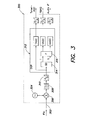
- FIG. 3 is a block diagram illustration of a digitally implemented television receiver with this type of circuit
- FIG. 4 is a block diagram illustration of a prior art synchronous demodulator for recovering a carrier
- FIG. 5 is a baseband graph for a frequency-modulated television signal of a prior art synchronous demodulator.
- FIG. 6 is a graph of a demodulated video signal for a frequency-modulated picture carrier and slow recovery of the carrier based on prior art.
- FIG. 1 illustrates a circuit 100 to effect carrier recovery of a reconstructed carrier for an input signal in, specifically, a television signal input on a line 102 .
- the individual components described may be designed as individual and separate structural elements. Implementation is also possible in the form of an integrated circuit or software in a processor, to the extent this is feasible for the individual components.
- the input signal on the line 102 is input to a mixer 104 , which includes multipliers 106 , 108 that generate in-phase and quadrature signal components, respectively.
- the in-phase and quadrature signal components are filtered by low-pass filters 110 , 112 , respectively and the resultant I and Q signal components are output on lines 114 , 116 , respectively.
- a carrier signal tr is applied in the known manner such that after multiplication of the input signal by the carrier signal an in-phase and a quadrature-phase signal are outputted at the respective outputs of multipliers.
- the I, Q signal components on lines 114 , 116 are input to a phase-locked loop (PLL) 120 and to a first processing unit 122 with a CORDIC 124 .
- PLL phase-locked loop
- the two components of the mixed signal i, q are fed to low-pass filters 130 , 132 if, for example, in the case of a television signal audio information must be removed.
- the output signals of the two low-pass filters 130 , 132 are then fed to the CORDIC 124 for processing. Since the phase value of the I/Q signal pair determined by the CORDIC 124 at its input is important in terms of later considerations, for the sake of simplification this value is shown only in FIG. 1 and then taken into account subsequently. Also for the sake of simplification, additional signals as well as components normally found within such a circuit are not considered and should be added as dictated by common technical knowledge.
- the signal output on the line 134 by the CORDIC 124 is fed along with the specific instantaneous phase value to a control device 136 which generates and provides a control correction signal on a line 138 to a local oscillator 140 .
- the local oscillator 140 utilizes the control correction signal to adjust the carrier signal on the line 142 which is generated by the local oscillator 140 and is fed to the mixers for multiplication with input signal on the line 102 .
- This correction signal on the line 148 is fed as a control signal to a phase shifter 152 . Since a propagation time delay z ⁇ k is caused by the control loop, delay devices 154 , 156 delay the mixed signal i, q respectively by a corresponding value z ⁇ k .
- the output signal or its components from the delay devices 156 , 158 are fed to the two inputs of the phase shifter 152 .
- the phase shifter 152 uses the applied correction signal on the line 138 to provide for a correction of the residual phase error of the mixed signal i, q, and outputs in-phase and quadrature corrected signals on lines 160 , 162 , respectively.
- the phase shifter 152 can also be designed based on independent components for the two signal components i, q of the mixed signal.
- FIG. 3 is a block diagram of a digitally implemented television receiver 300 in which a carrier recovery circuit of the present invention can be implemented.
- a received television signal IFin on a line 302 is converted by a local oscillator 304 and mixer 306 to a second intermediate frequency.
- a bandpass filter 308 After bandpass filtering in a bandpass filter 308 , unwanted mixing products are removed from the signal which can then be digitized without aliasing in an analog-to-digital converter A/D 310 .
- the resultant digitized signal is input to a digital signal processor (DSP) 312 , and mixed by a synchronous demodulator 314 into the baseband.
- DSP digital signal processor
- a video signal and audio intermediate-frequency signal are obtained from the I, Q signals, outputted from the synchronous demodulator 314 .
- an automatic gain control (AGC) tuner a tuner output level is adjusted so that the analog-to-digital converter A/D 310 is not overloaded.
- VAGC video AGC
- AAGC audio AGC
- signals to be outputted are modulated in an optimum manner for the corresponding digital-to-analog converters.
- the digital-to-analog converters output corresponding known signals tuner-AGC, FBAS (composite color video signal) or audio-IF (audio intermediate frequency) to additional components of a television receiver.
- the circuit of FIG. 1 can be advantageously employed as the synchronous demodulator 314 .
- the synchronous demodulator of FIG. 1 can also be advantageously employed in other receiver systems.
- the theoretical principles for reception of analog television signals are shown merely as an exemplary description.
- u ( t ) û BT ⁇ cos(2 ⁇ f BT ( t ) ⁇ t ) ⁇ (1 +m ⁇ Uêt ( t )) (2) as picture AM-modulation.
- the picture carrier frequency is altered as a function of time. It can change in a purely random fashion, for example as a result of phase jitter from the transmitter, or as a function of the amplitude of the video signal in the form of additional frequency modulation.
- the known carrier recovery loop is augmented, as shown in FIG. 1 , by a forward supervision that corrects the residual phase error via the phase shifter 152 ( FIG. 1 ) in the actual signal path following the mixer 104 and following the tap for the control loop.
- the delay devices 156 , 158 are used to adjust the system delay z ⁇ k of the filtering and phase measurement in the signal path so that the appropriate phase error is simultaneously applied for each I/Q value pair of mixed signal i, q at the input of the phase shifter 152 .
- the phase shifter 152 can be implemented, for example, by employing the known CORDIC algorithm. Implementation of the phase shifter 152 is also feasible using complex multiplication that can be executed according to the equations
- the correction signal TP-ph on the line 148 for the phase shifter 152 is generated, as described above, from the phase value ph on the line 134 by the low-pass filter 146 in the forward correction path, this value being output by the CORDIC 124 .
- this low-pass filter 146 it is possible to adjust the bandwidth of the error correction. This property is advantageous, for example, in allowing the broadband phase jitter of the transmitting oscillator to be excluded from the correction.
- the loop of the control loop is often set to a lower sampling rate.
- the other low-pass filter 146 can be designed to have either an additional or alternative function as an interpolation filter to recover the original sampling rate.
- FIGS. 2A and 2B show simulation results for a simulation of the entire system.
- the example here graphs a demodulated television signal, specifically, an FBAS signal, based on a simple implementation of the control loop (PLL), as a first signal a relative to a second signal b with an additional correction of the residual phase error.
- the graph here emphasizes the horizontal synchronization pulses or vertical synchronization pulses which without utilization of the forward correction as first signals a both exhibit significant distortions, with the result that a connected television set is not able to generate a stable picture from the signal.
- the juxtaposed second signals b exhibit correctly demodulated synchronization pulses.
Abstract
Description
u(t)=û BT·cos(2πf BT(t)·t)·(1+m·U Bild(t))+û TT·cos(2πf TT ·t+Δφ TT ·U Ton(t)), (1)
the first term corresponding to a picture AM modulation and the second term corresponding to an audio FM modulation where ûBT is the picture carrier amplitude, m is the modulation index, UBild(t) is the picture information, fBT(t) is the picture carrier frequency, ûTT is the audio carrier amplitude, fTT is the audio carrier frequency, ΔφTT is the phase deviation of the FM modulation, and UTon(t) is audio information.
u(t)=û BT·cos(2πf BT(t)·t)·(1+m·U Bild(t)) (2)
as picture AM-modulation.
Claims (4)
Applications Claiming Priority (3)
| Application Number | Priority Date | Filing Date | Title |
|---|---|---|---|
| DE102004047424 | 2004-09-28 | ||
| DE102004047424A DE102004047424A1 (en) | 2004-09-28 | 2004-09-28 | Circuit and method for carrier recovery |
| DE102004047424.9 | 2004-09-28 |
Publications (2)
| Publication Number | Publication Date |
|---|---|
| US20060067431A1 US20060067431A1 (en) | 2006-03-30 |
| US8098769B2 true US8098769B2 (en) | 2012-01-17 |
Family
ID=35500838
Family Applications (1)
| Application Number | Title | Priority Date | Filing Date |
|---|---|---|---|
| US11/237,611 Expired - Fee Related US8098769B2 (en) | 2004-09-28 | 2005-09-28 | Circuit and method for recovering a carrier |
Country Status (6)
| Country | Link |
|---|---|
| US (1) | US8098769B2 (en) |
| EP (1) | EP1641205B1 (en) |
| JP (1) | JP2006121677A (en) |
| KR (1) | KR100738732B1 (en) |
| CN (1) | CN1770752B (en) |
| DE (2) | DE102004047424A1 (en) |
Cited By (2)
| Publication number | Priority date | Publication date | Assignee | Title |
|---|---|---|---|---|
| US20090154616A1 (en) * | 2007-12-13 | 2009-06-18 | Jin Eun Sook | Residual frequency offset compensation apparatus using phase shift compensation scheme |
| US20100002810A1 (en) * | 2008-07-01 | 2010-01-07 | Fujitsu Limited | Adaptive optimization method and apparatus for average length |
Families Citing this family (7)
| Publication number | Priority date | Publication date | Assignee | Title |
|---|---|---|---|---|
| DE102004048572A1 (en) * | 2004-10-04 | 2006-04-13 | Micronas Gmbh | Method and circuit arrangement for suppressing an orthogonal disturbance |
| JP2006237819A (en) * | 2005-02-23 | 2006-09-07 | Nec Corp | Demodulator and phase compensation method therefor |
| DE102006017868A1 (en) | 2006-04-13 | 2007-10-18 | Micronas Gmbh | Method and circuit for carrier control in a quadrature demodulator |
| US7688918B2 (en) * | 2006-07-07 | 2010-03-30 | Alcatel-Lucent Usa Inc. | Recursive phase estimation for a phase-shift-keying receiver |
| CN103021470B (en) * | 2011-09-21 | 2016-08-03 | 瑞昱半导体股份有限公司 | Sampling phase correction method and the stocking system of this sampling phase correction method of use |
| WO2015061617A1 (en) * | 2013-10-24 | 2015-04-30 | Marvell World Trade Ltd. | Cartesian digital power amplifier using coordinate rotation |
| EP3217554B1 (en) * | 2016-03-11 | 2019-10-02 | Intel IP Corporation | Apparatuses and methods for compensating phase fluctuations |
Citations (63)
| Publication number | Priority date | Publication date | Assignee | Title |
|---|---|---|---|---|
| JPS5731235A (en) | 1980-08-01 | 1982-02-19 | Hitachi Denshi Ltd | Receiving system |
| EP0065150A1 (en) | 1981-05-20 | 1982-11-24 | TELEFUNKEN Fernseh und Rundfunk GmbH | IF amplifier for a multi-standard television receiver |
| US4484194A (en) | 1980-09-12 | 1984-11-20 | Telefonaktiebolaget L M Ericsson | Arrangement in a radar system for correction of phase and amplitude errors in a video signal |
| US4608703A (en) | 1983-05-12 | 1986-08-26 | Ricoh Company, Ltd. | Synchronization detection system for data transmission |
| JPS62233942A (en) | 1986-04-03 | 1987-10-14 | Nippon Telegr & Teleph Corp <Ntt> | Interference compensation circuit |
| US4729110A (en) | 1984-12-24 | 1988-03-01 | General Electric Company | Correction of offset and gain errors in RF receivers |
| US4860018A (en) | 1982-03-01 | 1989-08-22 | Western Atlas International, Inc. | Continuous wave interference rejection for reconstructed carrier receivers |
| US4871975A (en) | 1987-12-24 | 1989-10-03 | Nec Corporation | Carrier recovery circuit for offset QPSK demodulators |
| US4977580A (en) | 1988-08-15 | 1990-12-11 | Northern Telecom Limited | Timing and carrier recovery in TDMA without preamble sequence |
| US5148451A (en) | 1989-11-10 | 1992-09-15 | Nec Corporation | Carrier regeneration device correctly operable in mobile satellite communication |
| US5245611A (en) | 1991-05-31 | 1993-09-14 | Motorola, Inc. | Method and apparatus for providing carrier frequency offset compensation in a tdma communication system |
| JPH06104788A (en) | 1992-09-22 | 1994-04-15 | Toko Inc | Superheterodyne receiver |
| JPH06112858A (en) | 1992-09-29 | 1994-04-22 | Hitachi Ltd | Receiver |
| US5321514A (en) | 1986-05-14 | 1994-06-14 | Radio Telecom & Technology, Inc. | Interactive television and data transmission system |
| US5418815A (en) | 1992-06-12 | 1995-05-23 | Kabushiki Kaisha Toshiba | Receiver adaptively operable for multiple signal transmission systems |
| JPH07326980A (en) | 1994-06-02 | 1995-12-12 | Japan Radio Co Ltd | Receiver for mobile communication |
| EP0696854A1 (en) | 1994-08-08 | 1996-02-14 | THOMSON multimedia S.A. | Broadcast receiver adapted for analog and digital signals |
| US5507024A (en) | 1994-05-16 | 1996-04-09 | Allegro Microsystems, Inc. | FM data-system radio receiver |
| US5572264A (en) | 1994-02-14 | 1996-11-05 | Hitachi, Ltd. | High definition TV signal receiver |
| US5604768A (en) | 1992-01-09 | 1997-02-18 | Cellnet Data Systems, Inc. | Frequency synchronized bidirectional radio system |
| US5636312A (en) * | 1992-12-17 | 1997-06-03 | Pioneer Electronic Corporation | Video image mixing apparatus |
| JPH09294151A (en) | 1996-04-26 | 1997-11-11 | Hitachi Denshi Ltd | Digital modulator-demodulator |
| US5748262A (en) | 1995-05-23 | 1998-05-05 | Thomson Multimedia S.A. | Method of digitization of intermediate frequency signals in particular television signals, and device for implementation of the method |
| US5809088A (en) | 1995-07-14 | 1998-09-15 | Samsung Electronics Co., Ltd. | Digital carrier wave restoring device and method for use in a television signal receiver |
| US5825242A (en) | 1994-04-05 | 1998-10-20 | Cable Television Laboratories | Modulator/demodulator using baseband filtering |
| US5828705A (en) | 1996-02-01 | 1998-10-27 | Kroeger; Brian W. | Carrier tracking technique and apparatus having automatic flywheel/tracking/reacquisition control and extended signal to noise ratio |
| US5831689A (en) | 1995-06-12 | 1998-11-03 | Thomson Multimedia S.A. | Method of digitization of intermediate frequency video signals and device for implementation of the method |
| DE19739645A1 (en) | 1997-09-10 | 1999-03-11 | Fraunhofer Ges Forschung | Clock signal or carrier signal recovery circuit for digital data signal |
| US5893025A (en) | 1995-04-13 | 1999-04-06 | Matsushita Electric Industrial Co., Ltd. | CATV converter for receiving both analog and digital signals |
| US5956374A (en) * | 1996-04-04 | 1999-09-21 | Fujitsu Limited | Jitter suppressing circuit |
| EP0963110A2 (en) | 1998-06-06 | 1999-12-08 | Micronas Intermetall GmbH | Frequency conversion arrangement for a composite television signal |
| US6005363A (en) * | 1998-11-06 | 1999-12-21 | Texas Instruments Incorporated | Method and apparatus for position error signal (PES) measurement in a disk drive servo system |
| JP2000049879A (en) | 1998-05-29 | 2000-02-18 | Matsushita Electric Ind Co Ltd | Receiver, transmitter-receiver and its method |
| US6028903A (en) * | 1997-03-31 | 2000-02-22 | Sun Microsystems, Inc. | Delay lock loop with transition recycling for clock recovery of NRZ run-length encoded serial data signals |
| US6075409A (en) | 1998-04-03 | 2000-06-13 | Motorola, Inc. | Demodulation method and arrangement |
| JP2000174835A (en) | 1998-12-02 | 2000-06-23 | Nippon Hoso Kyokai <Nhk> | Carrier synchronizing circuit, quadrature demodulating circuit and crosstalk wave removing device |
| US6133964A (en) | 1996-06-12 | 2000-10-17 | Samsung Electroncis Co., Ltd. | Digital demodulator and method therefor |
| WO2001005025A1 (en) | 1999-07-07 | 2001-01-18 | Siemens Aktiengesellschaft | Method and device for correcting a corrupted useful signal |
| US6184921B1 (en) | 1998-02-20 | 2001-02-06 | Samsung Electronics Co., Ltd. | Method for transmitting VSB digital TV with carrier frequency near co-channel NTSC audio carrier frequency |
| US6233295B1 (en) | 1998-08-26 | 2001-05-15 | Thomson Licensing S.A. | Segment sync recovery network for an HDTV receiver |
| US6259751B1 (en) | 1997-01-10 | 2001-07-10 | Samsung Electronics Co., Ltd. | Circuit and method for removing interference in digital communication system |
| US6304136B1 (en) | 1999-03-03 | 2001-10-16 | Level One Communications, Inc. | Reduced noise sensitivity, high performance FM demodulator circuit and method |
| US6307898B1 (en) | 1998-04-15 | 2001-10-23 | Mitsubishi Denki Kabushiki Kaisha | Phase error detector |
| JP2002044174A (en) | 2000-07-26 | 2002-02-08 | Hitachi Kokusai Electric Inc | Digital pll circuit and phase synchronization method |
| US20020097812A1 (en) | 2000-12-01 | 2002-07-25 | John Wiss | In-phase and quadrature-phase rebalancer |
| JP2002217992A (en) | 2001-01-17 | 2002-08-02 | Matsushita Electric Ind Co Ltd | Modulation device and modulation method |
| US6459693B1 (en) | 1998-07-07 | 2002-10-01 | Samsung Electronics, Co., Ltd. | Device and method for cancelling code interference in a CDMA communication system |
| US20030011412A1 (en) * | 2001-06-20 | 2003-01-16 | Reidar Stief | Delay locked loop |
| US6559899B1 (en) | 1999-06-22 | 2003-05-06 | Alps Electric Co., Ltd. | Digital blocks television tuner having simple baseband signal processing portion |
| US6614734B1 (en) * | 1999-03-16 | 2003-09-02 | Stmicroelectronics Sa | Process and device for controlling an incident optical beam for reading a track of information on a dynamic medium |
| US20030203728A1 (en) | 2002-04-26 | 2003-10-30 | Filipovic Daniel F. | DC removal techniques for wireless networking |
| US6661852B1 (en) | 1999-07-21 | 2003-12-09 | Raytheon Company | Apparatus and method for quadrature tuner error correction |
| JP2004112384A (en) | 2002-09-19 | 2004-04-08 | Nippon Telegr & Teleph Corp <Ntt> | Quadrature demodulation error compensating method and circuit thereof |
| US20040081257A1 (en) | 1998-11-03 | 2004-04-29 | Broadcom Corporation | Phase detectors in carrier recovery for offset QAM and VSB |
| EP1487166A2 (en) | 2003-06-13 | 2004-12-15 | The Directv Group, Inc. | Carrier synchronization using a preamble and scattered pilot blocks |
| US20050069055A1 (en) | 2003-09-26 | 2005-03-31 | Yun-Jeong Song | Method and apparatus for compensating I/Q imbalance by using variable loop gain in quadrature demodulator |
| US20050110540A1 (en) * | 2003-11-20 | 2005-05-26 | Jong-Tae Kwak | Delay locked loop and its control method |
| US20050232376A1 (en) | 2004-04-20 | 2005-10-20 | Fiean Liem | System/method for receiving ASK and FSK signals using a single RF receiver |
| US20060072686A1 (en) | 2004-10-04 | 2006-04-06 | Ingo Steinbach | Method and circuit arrangement for suppressing an orthogonal perturbation |
| US7107011B2 (en) | 2003-02-21 | 2006-09-12 | Fujitsu Limited | Interference measurement and evaluation system |
| US7133469B2 (en) | 2001-08-03 | 2006-11-07 | Nec Corporation | Quadrature demodulator |
| US7170945B2 (en) | 2000-07-18 | 2007-01-30 | Thomson Licensing | Method of determining parameters of an OFDM signal and associated receiver |
| US7593065B2 (en) | 2004-11-12 | 2009-09-22 | Micronas Gmbh | Method and circuit for channel filtering of analog or digitally modulated TV signals |
Family Cites Families (2)
| Publication number | Priority date | Publication date | Assignee | Title |
|---|---|---|---|---|
| US5983025A (en) * | 1995-06-07 | 1999-11-09 | International Business Machines Corporation | Computer system buffers for providing concurrency and avoid deadlock conditions between CPU accesses, local bus accesses, and memory accesses |
| JP3481486B2 (en) * | 1999-02-15 | 2003-12-22 | Necビューテクノロジー株式会社 | Digital demodulator |
-
2004
- 2004-09-28 DE DE102004047424A patent/DE102004047424A1/en not_active Ceased
-
2005
- 2005-08-22 DE DE502005010333T patent/DE502005010333D1/en active Active
- 2005-08-22 EP EP05018145A patent/EP1641205B1/en not_active Not-in-force
- 2005-09-22 KR KR1020050088412A patent/KR100738732B1/en not_active IP Right Cessation
- 2005-09-27 CN CN2005101069753A patent/CN1770752B/en not_active Expired - Fee Related
- 2005-09-28 JP JP2005281570A patent/JP2006121677A/en active Pending
- 2005-09-28 US US11/237,611 patent/US8098769B2/en not_active Expired - Fee Related
Patent Citations (63)
| Publication number | Priority date | Publication date | Assignee | Title |
|---|---|---|---|---|
| JPS5731235A (en) | 1980-08-01 | 1982-02-19 | Hitachi Denshi Ltd | Receiving system |
| US4484194A (en) | 1980-09-12 | 1984-11-20 | Telefonaktiebolaget L M Ericsson | Arrangement in a radar system for correction of phase and amplitude errors in a video signal |
| EP0065150A1 (en) | 1981-05-20 | 1982-11-24 | TELEFUNKEN Fernseh und Rundfunk GmbH | IF amplifier for a multi-standard television receiver |
| US4860018A (en) | 1982-03-01 | 1989-08-22 | Western Atlas International, Inc. | Continuous wave interference rejection for reconstructed carrier receivers |
| US4608703A (en) | 1983-05-12 | 1986-08-26 | Ricoh Company, Ltd. | Synchronization detection system for data transmission |
| US4729110A (en) | 1984-12-24 | 1988-03-01 | General Electric Company | Correction of offset and gain errors in RF receivers |
| JPS62233942A (en) | 1986-04-03 | 1987-10-14 | Nippon Telegr & Teleph Corp <Ntt> | Interference compensation circuit |
| US5321514A (en) | 1986-05-14 | 1994-06-14 | Radio Telecom & Technology, Inc. | Interactive television and data transmission system |
| US4871975A (en) | 1987-12-24 | 1989-10-03 | Nec Corporation | Carrier recovery circuit for offset QPSK demodulators |
| US4977580A (en) | 1988-08-15 | 1990-12-11 | Northern Telecom Limited | Timing and carrier recovery in TDMA without preamble sequence |
| US5148451A (en) | 1989-11-10 | 1992-09-15 | Nec Corporation | Carrier regeneration device correctly operable in mobile satellite communication |
| US5245611A (en) | 1991-05-31 | 1993-09-14 | Motorola, Inc. | Method and apparatus for providing carrier frequency offset compensation in a tdma communication system |
| US5604768A (en) | 1992-01-09 | 1997-02-18 | Cellnet Data Systems, Inc. | Frequency synchronized bidirectional radio system |
| US5418815A (en) | 1992-06-12 | 1995-05-23 | Kabushiki Kaisha Toshiba | Receiver adaptively operable for multiple signal transmission systems |
| JPH06104788A (en) | 1992-09-22 | 1994-04-15 | Toko Inc | Superheterodyne receiver |
| JPH06112858A (en) | 1992-09-29 | 1994-04-22 | Hitachi Ltd | Receiver |
| US5636312A (en) * | 1992-12-17 | 1997-06-03 | Pioneer Electronic Corporation | Video image mixing apparatus |
| US5572264A (en) | 1994-02-14 | 1996-11-05 | Hitachi, Ltd. | High definition TV signal receiver |
| US5825242A (en) | 1994-04-05 | 1998-10-20 | Cable Television Laboratories | Modulator/demodulator using baseband filtering |
| US5507024A (en) | 1994-05-16 | 1996-04-09 | Allegro Microsystems, Inc. | FM data-system radio receiver |
| JPH07326980A (en) | 1994-06-02 | 1995-12-12 | Japan Radio Co Ltd | Receiver for mobile communication |
| EP0696854A1 (en) | 1994-08-08 | 1996-02-14 | THOMSON multimedia S.A. | Broadcast receiver adapted for analog and digital signals |
| US5893025A (en) | 1995-04-13 | 1999-04-06 | Matsushita Electric Industrial Co., Ltd. | CATV converter for receiving both analog and digital signals |
| US5748262A (en) | 1995-05-23 | 1998-05-05 | Thomson Multimedia S.A. | Method of digitization of intermediate frequency signals in particular television signals, and device for implementation of the method |
| US5831689A (en) | 1995-06-12 | 1998-11-03 | Thomson Multimedia S.A. | Method of digitization of intermediate frequency video signals and device for implementation of the method |
| US5809088A (en) | 1995-07-14 | 1998-09-15 | Samsung Electronics Co., Ltd. | Digital carrier wave restoring device and method for use in a television signal receiver |
| US5828705A (en) | 1996-02-01 | 1998-10-27 | Kroeger; Brian W. | Carrier tracking technique and apparatus having automatic flywheel/tracking/reacquisition control and extended signal to noise ratio |
| US5956374A (en) * | 1996-04-04 | 1999-09-21 | Fujitsu Limited | Jitter suppressing circuit |
| JPH09294151A (en) | 1996-04-26 | 1997-11-11 | Hitachi Denshi Ltd | Digital modulator-demodulator |
| US6133964A (en) | 1996-06-12 | 2000-10-17 | Samsung Electroncis Co., Ltd. | Digital demodulator and method therefor |
| US6259751B1 (en) | 1997-01-10 | 2001-07-10 | Samsung Electronics Co., Ltd. | Circuit and method for removing interference in digital communication system |
| US6028903A (en) * | 1997-03-31 | 2000-02-22 | Sun Microsystems, Inc. | Delay lock loop with transition recycling for clock recovery of NRZ run-length encoded serial data signals |
| DE19739645A1 (en) | 1997-09-10 | 1999-03-11 | Fraunhofer Ges Forschung | Clock signal or carrier signal recovery circuit for digital data signal |
| US6184921B1 (en) | 1998-02-20 | 2001-02-06 | Samsung Electronics Co., Ltd. | Method for transmitting VSB digital TV with carrier frequency near co-channel NTSC audio carrier frequency |
| US6075409A (en) | 1998-04-03 | 2000-06-13 | Motorola, Inc. | Demodulation method and arrangement |
| US6307898B1 (en) | 1998-04-15 | 2001-10-23 | Mitsubishi Denki Kabushiki Kaisha | Phase error detector |
| JP2000049879A (en) | 1998-05-29 | 2000-02-18 | Matsushita Electric Ind Co Ltd | Receiver, transmitter-receiver and its method |
| EP0963110A2 (en) | 1998-06-06 | 1999-12-08 | Micronas Intermetall GmbH | Frequency conversion arrangement for a composite television signal |
| US6459693B1 (en) | 1998-07-07 | 2002-10-01 | Samsung Electronics, Co., Ltd. | Device and method for cancelling code interference in a CDMA communication system |
| US6233295B1 (en) | 1998-08-26 | 2001-05-15 | Thomson Licensing S.A. | Segment sync recovery network for an HDTV receiver |
| US20040081257A1 (en) | 1998-11-03 | 2004-04-29 | Broadcom Corporation | Phase detectors in carrier recovery for offset QAM and VSB |
| US6005363A (en) * | 1998-11-06 | 1999-12-21 | Texas Instruments Incorporated | Method and apparatus for position error signal (PES) measurement in a disk drive servo system |
| JP2000174835A (en) | 1998-12-02 | 2000-06-23 | Nippon Hoso Kyokai <Nhk> | Carrier synchronizing circuit, quadrature demodulating circuit and crosstalk wave removing device |
| US6304136B1 (en) | 1999-03-03 | 2001-10-16 | Level One Communications, Inc. | Reduced noise sensitivity, high performance FM demodulator circuit and method |
| US6614734B1 (en) * | 1999-03-16 | 2003-09-02 | Stmicroelectronics Sa | Process and device for controlling an incident optical beam for reading a track of information on a dynamic medium |
| US6559899B1 (en) | 1999-06-22 | 2003-05-06 | Alps Electric Co., Ltd. | Digital blocks television tuner having simple baseband signal processing portion |
| WO2001005025A1 (en) | 1999-07-07 | 2001-01-18 | Siemens Aktiengesellschaft | Method and device for correcting a corrupted useful signal |
| US6661852B1 (en) | 1999-07-21 | 2003-12-09 | Raytheon Company | Apparatus and method for quadrature tuner error correction |
| US7170945B2 (en) | 2000-07-18 | 2007-01-30 | Thomson Licensing | Method of determining parameters of an OFDM signal and associated receiver |
| JP2002044174A (en) | 2000-07-26 | 2002-02-08 | Hitachi Kokusai Electric Inc | Digital pll circuit and phase synchronization method |
| US20020097812A1 (en) | 2000-12-01 | 2002-07-25 | John Wiss | In-phase and quadrature-phase rebalancer |
| JP2002217992A (en) | 2001-01-17 | 2002-08-02 | Matsushita Electric Ind Co Ltd | Modulation device and modulation method |
| US20030011412A1 (en) * | 2001-06-20 | 2003-01-16 | Reidar Stief | Delay locked loop |
| US7133469B2 (en) | 2001-08-03 | 2006-11-07 | Nec Corporation | Quadrature demodulator |
| US20030203728A1 (en) | 2002-04-26 | 2003-10-30 | Filipovic Daniel F. | DC removal techniques for wireless networking |
| JP2004112384A (en) | 2002-09-19 | 2004-04-08 | Nippon Telegr & Teleph Corp <Ntt> | Quadrature demodulation error compensating method and circuit thereof |
| US7107011B2 (en) | 2003-02-21 | 2006-09-12 | Fujitsu Limited | Interference measurement and evaluation system |
| EP1487166A2 (en) | 2003-06-13 | 2004-12-15 | The Directv Group, Inc. | Carrier synchronization using a preamble and scattered pilot blocks |
| US20050069055A1 (en) | 2003-09-26 | 2005-03-31 | Yun-Jeong Song | Method and apparatus for compensating I/Q imbalance by using variable loop gain in quadrature demodulator |
| US20050110540A1 (en) * | 2003-11-20 | 2005-05-26 | Jong-Tae Kwak | Delay locked loop and its control method |
| US20050232376A1 (en) | 2004-04-20 | 2005-10-20 | Fiean Liem | System/method for receiving ASK and FSK signals using a single RF receiver |
| US20060072686A1 (en) | 2004-10-04 | 2006-04-06 | Ingo Steinbach | Method and circuit arrangement for suppressing an orthogonal perturbation |
| US7593065B2 (en) | 2004-11-12 | 2009-09-22 | Micronas Gmbh | Method and circuit for channel filtering of analog or digitally modulated TV signals |
Non-Patent Citations (4)
| Title |
|---|
| J. Ammer et al., "Timing Recovery Unit for a 1.6 Mbps DSSS Receiver," [Online] Dec. 12, 2000, pp. 1-28, XP-002448107, University of Berkeley, USA, URL: http://bwrc.eecs.berkeley.edu/People/Grad-Students/msheets/ee225c/EE225c-final-ammer-sheets.pdf. |
| Japanese Office Action, Apr. 13, 2010. |
| Limann, "Fernsehtechnik ohne Ballast", Einfuhrung in die Schaltungstechnik der Schwarzweiss- und Farb-Fernsehempfanger, 13th edition, 1979, Franzis-Verlag GmbH, Munich; ISBN 3-7723-5273-1; pp. 73-85. |
| W. Gao et al., "All-Digital Reverse Modulation Architecture Based Carrier Recovery Implementation for GMSK and Compatible FQPSK," IEEE Transactions on Broadcasting, vol. 42, No. 1, Mar. 1996, pp. 55-62, XP011006019. |
Cited By (3)
| Publication number | Priority date | Publication date | Assignee | Title |
|---|---|---|---|---|
| US20090154616A1 (en) * | 2007-12-13 | 2009-06-18 | Jin Eun Sook | Residual frequency offset compensation apparatus using phase shift compensation scheme |
| US20100002810A1 (en) * | 2008-07-01 | 2010-01-07 | Fujitsu Limited | Adaptive optimization method and apparatus for average length |
| US8189718B2 (en) * | 2008-07-01 | 2012-05-29 | Fujitsu Limited | Adaptive optimization method and apparatus for average length |
Also Published As
| Publication number | Publication date |
|---|---|
| DE102004047424A1 (en) | 2006-04-06 |
| CN1770752A (en) | 2006-05-10 |
| EP1641205A2 (en) | 2006-03-29 |
| JP2006121677A (en) | 2006-05-11 |
| EP1641205B1 (en) | 2010-10-06 |
| EP1641205A3 (en) | 2007-10-03 |
| CN1770752B (en) | 2010-12-08 |
| US20060067431A1 (en) | 2006-03-30 |
| KR100738732B1 (en) | 2007-07-12 |
| DE502005010333D1 (en) | 2010-11-18 |
| KR20060051544A (en) | 2006-05-19 |
Similar Documents
| Publication | Publication Date | Title |
|---|---|---|
| US8098769B2 (en) | Circuit and method for recovering a carrier | |
| US6133964A (en) | Digital demodulator and method therefor | |
| US8093943B2 (en) | Phase noise correction device and its method | |
| US5809088A (en) | Digital carrier wave restoring device and method for use in a television signal receiver | |
| EP2053737A2 (en) | Signal processing device and method, and digital broadcast receiving device, and method | |
| US6731698B1 (en) | Quadrature demodulation circuit capable for canceling offset | |
| US5533059A (en) | Carrier phase lock detecting apparatus used in PSK-modulated signal receiver for satellite communication system | |
| JP4579458B2 (en) | Demodulator, broadcast system and semiconductor device | |
| US5914985A (en) | Digital demodulator | |
| US20050220241A1 (en) | Mean power frequency discriminator, frequency phase locked loop circuit and digital television demodulator using the same | |
| US6570441B1 (en) | Incoherent demodulator and method of incoherently demodulating an IF signal | |
| US5371902A (en) | Method and apparatus for recovering baseband signals from in-phase and quadrature-phase signal components having phase error therebetween | |
| US7110475B2 (en) | Digital TV receiver | |
| US4686569A (en) | Circuitry for reducing demodulation phase error as for an automatic deghosting system | |
| US7920653B2 (en) | Method and circuit arrangement for suppressing an orthogonal perturbation | |
| JPH0974431A (en) | Carrier phase synchronization circuit | |
| EP1988639B1 (en) | Receiving apparatus | |
| JP3537738B2 (en) | Clock recovery circuit | |
| JP2765601B2 (en) | Demodulation circuit | |
| JP3413359B2 (en) | QPSK demodulator | |
| JP2002217992A (en) | Modulation device and modulation method | |
| JPH0936924A (en) | Multilevel fsk reception equipment | |
| JP3578650B2 (en) | Carrier synchronization circuit, quadrature demodulation circuit and interference wave canceller | |
| JP3382892B2 (en) | Method and apparatus for detecting a frame synchronization pattern by digitally demodulating a phase modulated signal in hierarchical transmission | |
| JPH0479499B2 (en) |
Legal Events
| Date | Code | Title | Description |
|---|---|---|---|
| AS | Assignment |
Owner name: MICRONAS GMBH, GERMANY Free format text: ASSIGNMENT OF ASSIGNORS INTEREST;ASSIGNOR:STEINBACH, INGO;REEL/FRAME:016965/0028 Effective date: 20051026 |
|
| AS | Assignment |
Owner name: TRIDENT MICROSYSTEMS (FAR EAST) LTD.,CAYMAN ISLAND Free format text: ASSIGNMENT OF ASSIGNORS INTEREST;ASSIGNOR:MICRONAS GMBH;REEL/FRAME:024456/0453 Effective date: 20100408 Owner name: TRIDENT MICROSYSTEMS (FAR EAST) LTD., CAYMAN ISLAN Free format text: ASSIGNMENT OF ASSIGNORS INTEREST;ASSIGNOR:MICRONAS GMBH;REEL/FRAME:024456/0453 Effective date: 20100408 |
|
| AS | Assignment |
Owner name: ENTROPIC COMMUNICATIONS, INC., CALIFORNIA Free format text: ASSIGNMENT OF ASSIGNORS INTEREST;ASSIGNORS:TRIDENT MICROSYSTEMS, INC.;TRIDENT MICROSYSTEMS (FAR EAST) LTD.;REEL/FRAME:028153/0530 Effective date: 20120411 |
|
| REMI | Maintenance fee reminder mailed | ||
| LAPS | Lapse for failure to pay maintenance fees | ||
| STCH | Information on status: patent discontinuation |
Free format text: PATENT EXPIRED DUE TO NONPAYMENT OF MAINTENANCE FEES UNDER 37 CFR 1.362 |
|
| FP | Lapsed due to failure to pay maintenance fee |
Effective date: 20160117 |