US8099655B1 - Galois field multiplier system and method - Google Patents
Galois field multiplier system and method Download PDFInfo
- Publication number
- US8099655B1 US8099655B1 US11/961,494 US96149407A US8099655B1 US 8099655 B1 US8099655 B1 US 8099655B1 US 96149407 A US96149407 A US 96149407A US 8099655 B1 US8099655 B1 US 8099655B1
- Authority
- US
- United States
- Prior art keywords
- circuit
- receiving
- bit
- inputs
- input
- Prior art date
- Legal status (The legal status is an assumption and is not a legal conclusion. Google has not performed a legal analysis and makes no representation as to the accuracy of the status listed.)
- Active, expires
Links
Images


Classifications
-
- H—ELECTRICITY
- H03—ELECTRONIC CIRCUITRY
- H03M—CODING; DECODING; CODE CONVERSION IN GENERAL
- H03M13/00—Coding, decoding or code conversion, for error detection or error correction; Coding theory basic assumptions; Coding bounds; Error probability evaluation methods; Channel models; Simulation or testing of codes
- H03M13/03—Error detection or forward error correction by redundancy in data representation, i.e. code words containing more digits than the source words
- H03M13/05—Error detection or forward error correction by redundancy in data representation, i.e. code words containing more digits than the source words using block codes, i.e. a predetermined number of check bits joined to a predetermined number of information bits
- H03M13/13—Linear codes
- H03M13/15—Cyclic codes, i.e. cyclic shifts of codewords produce other codewords, e.g. codes defined by a generator polynomial, Bose-Chaudhuri-Hocquenghem [BCH] codes
- H03M13/151—Cyclic codes, i.e. cyclic shifts of codewords produce other codewords, e.g. codes defined by a generator polynomial, Bose-Chaudhuri-Hocquenghem [BCH] codes using error location or error correction polynomials
- H03M13/158—Finite field arithmetic processing
-
- H—ELECTRICITY
- H03—ELECTRONIC CIRCUITRY
- H03M—CODING; DECODING; CODE CONVERSION IN GENERAL
- H03M13/00—Coding, decoding or code conversion, for error detection or error correction; Coding theory basic assumptions; Coding bounds; Error probability evaluation methods; Channel models; Simulation or testing of codes
- H03M13/03—Error detection or forward error correction by redundancy in data representation, i.e. code words containing more digits than the source words
- H03M13/05—Error detection or forward error correction by redundancy in data representation, i.e. code words containing more digits than the source words using block codes, i.e. a predetermined number of check bits joined to a predetermined number of information bits
- H03M13/13—Linear codes
- H03M13/15—Cyclic codes, i.e. cyclic shifts of codewords produce other codewords, e.g. codes defined by a generator polynomial, Bose-Chaudhuri-Hocquenghem [BCH] codes
- H03M13/151—Cyclic codes, i.e. cyclic shifts of codewords produce other codewords, e.g. codes defined by a generator polynomial, Bose-Chaudhuri-Hocquenghem [BCH] codes using error location or error correction polynomials
- H03M13/1515—Reed-Solomon codes
Definitions
- the present invention relates generally to Galois Field multiplication.
- the present invention relates to a Galois Field multiplication method and system that allows the multiplication of any two Galois field polynomials for any given primitive polynomial.
- errors can occur when storing, transmitting, or receiving digital signals. These errors are practically unavoidable due to inherent noise present on the transmission media and the storing/receiving systems.
- several methods such as, for example, Reed Solomon coding, have been developed to detect and correct errors.
- RAID Redundant Arrays of Inexpensive Disks
- the “RAID level 5” configuration also called the “N+1 parity” technique, provides a simple solution to calculate the checksum by performing bitwise exclusive-or (XOR) of the data bytes distributed to all storage devices. If one of the N+1 devices fails, the data can be reconstructed by XOR-ing the data of the remaining N devices.
- N+1 parity is attractive because of its simplicity; however, it requires one extra storage device and one extra write operation per write to any single device. Its main disadvantage is that it cannot recover from more than one simultaneous storage device failure.
- the “RAID level 6” configuration provides better error recovery by not only generating P checksum parity (p parity) as defined in RAID level 5, but also generating Q checksum parity (q parity) by adopting an error correction algorithm through Galois Field (GF) multiplication with a primitive polynomial. If any two of the N+2 devices fails, the failing devices can be reconstructed by using the P and Q checksums together with the remaining N devices.
- GF Galois Field
- GF arithmetic is a cyclic finite field arithmetic meaning that any operation performed on any two numbers within the field yields a number in the field, i.e., there is no arithmetic operation that can be done on any two numbers within the field that will produce a number outside of the field. Since digital systems transmit/store data in bits, which can only take on one of two values (0 or 1), grouping these bits together to build a symbol is common in digital systems and these groupings are all based on powers of two. Table 1 shows the relationship between the number of bits per symbol, the equivalent range of integers spanned by the number of bits, and the equivalent GF representation.
- Galois field arithmetic uses the numbers shown in Table 1. For example, the range of integers from 0 to 7 (0, 1, 2, 3, 4, 5, 6, 7) has a Galois Field representation or notation of GF(8) because the Galois Field has 8 elements, while the range of integers 0 to 1 has a Galois Field of GF(2) because it has only two elements, etc.
- each GF can have one or more primitive polynomials, also called generator polynomials, which is analogous to a particular set of consecutive real integers. These one or more primitive polynomials include one or more prime numbers, depending upon how large is the particular set of consecutive integers.
- the primitive polynomials, p(x) are used to define the arithmetic functions for each GF and to ensure that each GF arithmetic operation yields a result that is part of the GF in question. For example, in GF arithmetic, as in basic arithmetic, certain mathematical properties, such as, for example, commutativity and associativity exist.
- the primitive polynomials are represented by the decimal number 11 (1011 binary, x 3 +x+1 polynomial) and by the decimal number 19 (10011 binary, x 4 +x+1 polynomial).
- GF(128) has 9 primitive polynomials and GF(256) has 8 primitive polynomials.
- the most commonly used approach in multiplying two values of a GF is to generate two logarithm tables, which converts the multiplication process into three lookup tables and an addition. These tables can be referred to as gflog[ ] (GF logarithm) and gfilog[ ] (GF inverse logarithm).
- the gflog[ ] table is defined for the indices 1 to 2m ⁇ 1, and maps the index to its logarithm in the GF.
- the gfilog[ ] table it is defined for the indices 0 to 2m ⁇ 2, and maps the index to its inverse logarithm in the GF.
- the advantage of using the table lookup approach is that it supports all kinds of primitive polynomial by simply updating the lookup tables with different index mapping values. However, this approach is similar to the brute approach in that it is quite slow.
- the present invention provides a multiplier circuit for multiplying a first polynomial B(x) by a second polynomial C(x), B(x) and C(x) being part of a Galois field GF(2m) and being representable in binary format as B[m ⁇ 1:0] and C[m ⁇ 1:0] respectively.
- the multiplier circuit comprises a first sub-circuit having: a first logic gate unit having a first group of inputs, each input of the first group of inputs for receiving bit B[m ⁇ 1], the first logic gate unit further having a second group of inputs, each input of the second group of inputs for receiving the bits of a primitive polynomial P(x) of GF(2m), P(x) being representable in binary format as P[m ⁇ 1:0], the first logic gate unit for multiplying the first group of inputs and the second group of inputs to obtain (B[m ⁇ 1]*P[m ⁇ 1:0])[m ⁇ 1:0]; a shifting device for receiving B[m ⁇ 1:0] and for shifting by 1 bit to the left the bits of B[m ⁇ 1:0] to obtain LS_B[m ⁇ 1:0]; and a second logic gate unit for receiving, and for adding, (B[m ⁇ 1]*P[m ⁇ 1:0])[m ⁇ 1:0] and LS_B[m
- the multiplier circuit also comprises a second sub-circuit having: an input for receiving (B(x)*x)[m ⁇ 1:0] from the first sub-circuit; inputs for receiving B[m ⁇ 1:0], C[m ⁇ 1:0] and P[m ⁇ 1:0]; and a logic unit for calculating, in accordance with (B(x)*x)[m ⁇ 1:0], B[m ⁇ 1:0], C[m ⁇ 1:0] and P[m ⁇ 1:0], (C[k]*B(x)*xk)[m ⁇ 1:0] for each value of k ranging from 0 to m ⁇ 1, k being an integer, and for summing together (C[k]*B(x)*xk)[m ⁇ 1:0] for k ranging from 0 to m ⁇ 1, to obtain (B(x)*C(x))[m ⁇ 1:0].
- the first logic gate unit of the first sub-circuit includes m AND-gates, an input of each AND-gate for receiving bit B[m ⁇ 1], another input of each AND-gate for receiving one of the m bits of P[m ⁇ 1:0].
- the shifting device of the first sub-circuit is a shift-register.
- the second logic gate unit of the first sub-circuit includes m XOR-gates, an input of each XOR-gate for receiving a bit of (B[m ⁇ 1]*P[m ⁇ 1:0])[m ⁇ 1:0], another input of each XOR gate for receiving a corresponding bit of LS_B[m ⁇ 1:0].
- the method comprises steps of: multiplying bit B[m ⁇ 1] by a primitive polynomial P[m ⁇ 1:0] to obtain (B[m ⁇ 1]*P[m ⁇ 1:0])[m ⁇ 1:0]; left-shifting by one bit B[m ⁇ 1:0] to obtain LS_B[m ⁇ 1:0]; adding (B[m ⁇ 1]*P[m ⁇ 1:0])[m ⁇ 1:0] and LS_B[m ⁇ 1:0] to obtain (B(x)*x)[m ⁇ 1:0]; and, calculating, in accordance with (B(x)*x)[m ⁇ 1:0], B[m ⁇ 1:0], C[m ⁇ 1:0] and P[m ⁇ 1:0], (C[k]*B(x)*xk)[m ⁇ 1:0] for each value of k ranging from 0 to m ⁇ 1, k being an integer, and for summing together (C[k]*B(x)*xk)
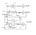
- FIG. 1 shows an exemplary functional block diagram of a Galois Field multiplier of the present invention
- FIG. 2 shows a multi-stage embodiment of the Galois Field multiplier of FIG. 1 ;
- FIG. 3 shows a single stage embodiment of the Galois Field multiplier of FIG. 1 .
- B ( x ) b m-1 x m-1 +b m-2 x m-2 + . . . +b 2 x 2 +b 1 x+b 0 (1)
- a GF multiplication operation is defined such that B*C satisfy GF ( B ⁇ C ) ⁇ GF (2 m ) (7) through the identity
- the computation of the B*C product can be broken down into 3 steps: (a) find the product of Bx i which involves (m ⁇ 1) constant multiplication operations done in parallel (this is represented by equation 11 and is referred to as P-box logic, which is shown in greater detail at FIG. 2 ); (b) find the product of c i (Bx i ) which involves AND-ing the value of c i with the value Bx i given that c i is a 1-bit number and can only be either 1 or 0; and (c) sum together all the products found in the step (b). This involves XOR-ing all the c i (Bx i ) m-bit vectors. The result of the summation is the product B*C.
- FIG. 1 shows an exemplary embodiment of a functional block diagram for a GF(2 m ) multiplier of the present invention.
- the P-box logic or function is defined by equation (11) and is shown at reference numeral 20 .
- This P-box logic uses the primitive polynomial (equation 8), which can be arbitrary, to perform the modulo operation defined by equation 11.
- the output of operation 22 is equal to the result of operation 20 multiplied by x.
- FIG. 2 shows an exemplary embodiment of a GF multiplier 10 of the present invention in a multi-stage pipeline design.
- the design comprises a plurality of functional units labeled as 30 , 32 and 34 , which can all perform the same functions, including those depicted for the functional unit 30 .
- the functional unit 30 includes a shift register 36 , or any other suitable type of shifting device, that receives the B[m ⁇ 1:0] input vector and shifts of the input vector by 1 bit to the left to produce LS_B[m ⁇ 1:0]. That is, bit 1 of B[m ⁇ 1:0] becomes bit 0 , bit 2 of B[m ⁇ 1:0] becomes bit 1 , etc.
- the output of the shift register 36 i.e., LS_B(x) (LS_B[m ⁇ 1:0]), is sent to m XOR gates shown as XOR-gate unit 38 , or to any other suitable type of logic gate unit.
- the functional unit 30 also comprises m AND gates shown as AND-gate unit 40 , or any other suitable type of logic gate unit, that receives Bit[m ⁇ 1] of the B[m ⁇ 1:0] input vector and the arbitrary input primitive polynomial P[m ⁇ 1:0].
- the outputs of the AND gate unit 40 which are either 0 or P[m ⁇ 1:0], are sent to the XOR-gate unit 38 where they are XOR-ed with the outputs of the shift register 36 .
- the GF multiplier 10 of FIG. 2 also includes m AND gates shown as AND-gate unit 42 , or any other suitable type of logic gate unit, that receives the m outputs of XOR-gate unit 38 , i.e., the outputs of the functional unit 30 , and multiplies them by c 1 .
- the outputs of the AND-gate unit 42 corresponds to the bits of the term c 1 *B*x of equation (10).
- the GF multiplier 10 further includes m other AND gates shown as AND-gate unit 44 , or any other suitable type of logic gate unit, that receives as input c 0 and the m bits of vector B[m ⁇ 1:0].
- the output of the functional unit 30 is also provided, as an input vector, to the functional unit 32 through an optional pipeline register 48 , the presence of which is decided, as would be understood by the skilled worker, in accordance with the timing margin of the GF multiplier 10 .
- the functional unit 32 also receives the primitive polynomial P[m ⁇ 1:0] and performs the same functions as the functional unit 30 .
- the output of the functional unit 32 which is equal to B(x)*x 2 , is provided as input to m AND gates shown as AND-gate unit 50 , or to any other suitable type of logic gate unit, that receives c 2 as another input.
- the outputs of the AND-gate unit 50 correspond to the bits of the term c 2 *B*x 2 of equation (10).
- the outputs of the AND-gate unit 50 is XOR-ed at m XOR gates shown as XOR-gate unit 52 , or at any other suitable type of logic gate unit, with the outputs of XOR-gate unit 46 .
- the outputs of the XOR-gate unit 52 correspond to the bits of the term (c 0 *B+c 1 *B*x+c 2 *B*x 2 ) of equation (10).
- the outputs of XOR-gate unit 46 can be provided to the inputs of XOR-gate unit 52 through an optional pipeline register 54 .
- the GF multiplier 10 further includes optional pipeline registers 56 , 58 and 60 ; AND-gate unit 62 ; XOR-gate unit 64 ; and, as mentioned above, the functional unit 34 .
- the outputs of the AND-gate unit 62 correspond to the bits of the term c m-1 *B*x m-1 of equation (10), and the output of XOR-gate unit 64 corresponds to GF(B*C).
- the AND-gate unit 62 and the XOR-gate unit 64 can be replaced by any other suitable logic gate units.
- FIG. 3 shows a single stage multiple-cycle embodiment GF multiplier of the present invention.
- the single stage GF multiplier (SSGFM) 70 includes a functional unit 72 that functions in the same way as the functional unit 30 described above with respect to FIG. 2 .
- the SSGFM 70 also includes a counter unit 74 for counting from 0 to m ⁇ 2, m being the relevant number of bits.
- the counter unit 74 is such that it produces an output equal to “1” when the count value is “0”, and produces an output equal to “0” when the count value is different from zero, i.e., it produces an output equal to “0” when the count value is comprised within the range [1, m ⁇ 2].
- the shift register 80 outputs the value c 1 , which acts as an input to AND-gate unit 82 , and multiplexer 84 outputs the vector B[m ⁇ 1:0] to functional unit 72 , the other input of which is the primitive polynomial P[m ⁇ 1:0].
- the functional units outputs the value B*x, which acts as the other input to AND-gate unit 82 . Therefore, the outputs of the AND-gate unit 82 are, upon the counter unit 74 having its count value set to “0”, the bits of c 1 *B*x.
- the SSGFM 70 can include registers 90 , 92 and 94 depending on the associated timing margin of the SSGFM 70 .
- the OR-gate 78 , the XOR-gate unit 86 , and the AND-gate units 82 , 88 can be replaced by any other suitable type of logic gate or logic gate unit without departing from the scope of the invention.
- the embodiments of the GF multipliers described herein can be implemented through programming of a digital signal processor through any suitable hardware description language such as, for example, VHDL (“Very-High-Speed Integrated Circuit” Hardware Description Language).
- VHDL Very-High-Speed Integrated Circuit
Abstract
Description
| TABLE 1 |
| Digital symbols vs. GF notation |
| Number | |||
| of bits | Galois Field | ||
| per symbol | Range of | representation | |
| 1 | 0 to 1 | GF(2) | |
| 2 | 0 to 3 | GF(4) | |
| 3 | 0 to 7 | GF(8) | |
| 4 | 0 to 15 | GF(16) | |
| 5 | 0 to 31 | GF(32) | |
| 6 | 0 to 63 | GF(64) | |
| 7 | 0 to 127 | GF(128) | |
| 8 | 0 to 255 | GF(256) | |
| |
0 to (2m − 1) | GF(2m) | |
| TABLE 2 |
| Representation of GF(8) |
| Integer | | Polynomial | |
| 0 | 000 | 0 | |
| 1 | 001 | 1 | |
| 2 | 010 | x | |
| 3 | 011 | x + 1 | |
| 4 | 100 | x2 | |
| 5 | 101 | x2 + 1 | |
| 6 | 110 | x2 + x | |
| 7 | 111 | x2 + x + 1 | |
| TABLE 3 |
| Primitive polynomials for Galois Fields |
| GF(x) | P(x) | GF(x) | P(x) | GF(x) | P(x) | |
| 8 | 11 | 128 | 137 | 256 | 285 | |
| 16 | 19 | 128 | 143 | 256 | 361 | |
| 32 | 37 | 128 | 157 | 256 | 487 | |
| 32 | 61 | 128 | 247 | 256 | 299 | |
| 32 | 55 | 128 | 191 | 256 | 357 | |
| 64 | 67 | 128 | 213 | 256 | 355 | |
| 64 | 103 | 128 | 131 | 256 | 351 | |
| 64 | 109 | 128 | 203 | 256 | 451 | |
| 128 | 229 | |||||
B(x)=b m-1 x m-1 +b m-2 x m-2 + . . . +b 2 x 2 +b 1 x+b 0 (1)
where the coefficient bi is either 1 or 0,
C(x)=c m-1 x m-1 +c m-2 x m-2 + . . . +c 2 x 2 +c 1 x+c 0 (3)
where the coefficient bi is either 1 or 0. As will be understood by the skilled worker, C(x) and B(x) can be expressed respectively as B[m−1:0] and C[m−1:0].
P(x)=p m-1 x m-1 +p m-2 x m-2 + . . . +p 2 x 2 +p 1 x+p 0 (5)
where the coefficient pi is either 1 or 0.
GF(B·C)εGF(2m) (7)
through the identity
that transforms an (m+1)-bit element (xm) into an m-bit element (P(x)) in order to preserve the GF.
where the coefficient ci is either 1 or 0 and where B(x)*C(x) can be expressed as (B(x)*C(x))[m−1:0].
Where equation (8) has been used and with LS_B meaning that the polynomial B has been shifted by 1 bit to the left. As will be understood by the skilled worker, LS_B can be expressed as LS_B[m−1:0]. As will be understood by the skilled worker the plus signs (+) used above are to be interpreted as XOR operations (⊕).
Claims (10)
Priority Applications (1)
| Application Number | Priority Date | Filing Date | Title |
|---|---|---|---|
| US11/961,494 US8099655B1 (en) | 2007-12-20 | 2007-12-20 | Galois field multiplier system and method |
Applications Claiming Priority (1)
| Application Number | Priority Date | Filing Date | Title |
|---|---|---|---|
| US11/961,494 US8099655B1 (en) | 2007-12-20 | 2007-12-20 | Galois field multiplier system and method |
Publications (1)
| Publication Number | Publication Date |
|---|---|
| US8099655B1 true US8099655B1 (en) | 2012-01-17 |
Family
ID=45445189
Family Applications (1)
| Application Number | Title | Priority Date | Filing Date |
|---|---|---|---|
| US11/961,494 Active 2030-11-15 US8099655B1 (en) | 2007-12-20 | 2007-12-20 | Galois field multiplier system and method |
Country Status (1)
| Country | Link |
|---|---|
| US (1) | US8099655B1 (en) |
Cited By (6)
| Publication number | Priority date | Publication date | Assignee | Title |
|---|---|---|---|---|
| US8370717B1 (en) * | 2008-04-08 | 2013-02-05 | Marvell International Ltd. | Method and apparatus for flexible buffers in an XOR engine |
| US8566652B1 (en) | 2007-12-26 | 2013-10-22 | Marvell International Ltd. | Command queuing in disk drives |
| US9311052B2 (en) | 2012-11-29 | 2016-04-12 | Electronics And Telecommunications Research Institute | Method of performing multiplication operation in binary extension finite field |
| US9473176B2 (en) * | 2014-11-27 | 2016-10-18 | Apple Inc. | Implementation of log and inverse operation in a Galois Field |
| US9804828B2 (en) | 2014-11-24 | 2017-10-31 | Apple Inc. | Cubic root of a galois field element |
| US10649841B2 (en) | 2018-03-05 | 2020-05-12 | Alibaba Group Holding Limited | Supporting multiple page lengths with unique error correction coding via galois field dimension folding |
Citations (25)
| Publication number | Priority date | Publication date | Assignee | Title |
|---|---|---|---|---|
| US4847801A (en) | 1987-10-26 | 1989-07-11 | Cyclotomics, Inc. | Compact galois field multiplier |
| US5379243A (en) | 1992-08-31 | 1995-01-03 | Comstream Corporation | Method and apparatus for performing finite field division |
| US5502665A (en) | 1993-11-20 | 1996-03-26 | Goldstar Co., Ltd. | Galois field multiplier |
| US5570378A (en) * | 1992-04-28 | 1996-10-29 | Mitsubishi Denki Kabushiki Kaisha | Error-correcting apparatus |
| US5689452A (en) | 1994-10-31 | 1997-11-18 | University Of New Mexico | Method and apparatus for performing arithmetic in large galois field GF(2n) |
| US5768168A (en) | 1996-05-30 | 1998-06-16 | Lg Semicon Co., Ltd. | Universal galois field multiplier |
| US6038581A (en) | 1997-01-29 | 2000-03-14 | Nippon Telegraph And Telephone Corporation | Scheme for arithmetic operations in finite field and group operations over elliptic curves realizing improved computational speed |
| US6134572A (en) | 1997-09-30 | 2000-10-17 | Texas Instruments Incorporated | Galois Field arithmetic apparatus and method |
| US6141786A (en) * | 1998-06-04 | 2000-10-31 | Intenational Business Machines Corporation | Method and apparatus for performing arithmetic operations on Galois fields and their extensions |
| US6286123B1 (en) * | 1997-07-13 | 2001-09-04 | Samsung Electronics Co., Ltd. | Circuit for calculating error position polynomial at high speed |
| US6366941B1 (en) | 1998-02-03 | 2002-04-02 | Texas Instruments Incorporated | Multi-dimensional Galois field multiplier |
| US6467063B1 (en) * | 1998-06-02 | 2002-10-15 | Matsushita Electric Industrial Co., Ltd. | Reed Solomon coding apparatus and Reed Solomon coding method |
| US6473779B1 (en) * | 1996-10-03 | 2002-10-29 | Texas Instruments Incorporated | Combinatorial polynomial multiplier for galois field 256 arithmetic |
| US6550035B1 (en) * | 1998-10-20 | 2003-04-15 | Texas Instruments Incorporated | Method and apparatus of Reed-Solomon encoding-decoding |
| US6694476B1 (en) * | 2000-06-02 | 2004-02-17 | Vitesse Semiconductor Corporation | Reed-solomon encoder and decoder |
| US6701336B1 (en) * | 1999-11-12 | 2004-03-02 | Maxtor Corporation | Shared galois field multiplier |
| US6760742B1 (en) | 2000-02-18 | 2004-07-06 | Texas Instruments Incorporated | Multi-dimensional galois field multiplier |
| US6766345B2 (en) | 2001-11-30 | 2004-07-20 | Analog Devices, Inc. | Galois field multiplier system |
| US6871315B2 (en) * | 2000-07-19 | 2005-03-22 | Nec Corporation | Decoding circuit and decoding method thereof |
| US7136892B2 (en) * | 2001-12-29 | 2006-11-14 | Koninklijke Philips Electronics N.V. | Method for multiplying two factors from the Galois field and multiplier for performing the method |
| US7178091B1 (en) * | 2001-07-10 | 2007-02-13 | National Semiconductor Corporation | Reed solomon encoder |
| US7313583B2 (en) * | 2002-10-22 | 2007-12-25 | Broadcom Corporation | Galois field arithmetic unit for use within a processor |
| US7526518B2 (en) * | 2004-10-13 | 2009-04-28 | Cisco Technology, Inc. | Galois field multiplication system and method |
| US7895253B2 (en) * | 2001-11-30 | 2011-02-22 | Analog Devices, Inc. | Compound Galois field engine and Galois field divider and square root engine and method |
| US8024551B2 (en) * | 2005-10-26 | 2011-09-20 | Analog Devices, Inc. | Pipelined digital signal processor |
-
2007
- 2007-12-20 US US11/961,494 patent/US8099655B1/en active Active
Patent Citations (25)
| Publication number | Priority date | Publication date | Assignee | Title |
|---|---|---|---|---|
| US4847801A (en) | 1987-10-26 | 1989-07-11 | Cyclotomics, Inc. | Compact galois field multiplier |
| US5570378A (en) * | 1992-04-28 | 1996-10-29 | Mitsubishi Denki Kabushiki Kaisha | Error-correcting apparatus |
| US5379243A (en) | 1992-08-31 | 1995-01-03 | Comstream Corporation | Method and apparatus for performing finite field division |
| US5502665A (en) | 1993-11-20 | 1996-03-26 | Goldstar Co., Ltd. | Galois field multiplier |
| US5689452A (en) | 1994-10-31 | 1997-11-18 | University Of New Mexico | Method and apparatus for performing arithmetic in large galois field GF(2n) |
| US5768168A (en) | 1996-05-30 | 1998-06-16 | Lg Semicon Co., Ltd. | Universal galois field multiplier |
| US6473779B1 (en) * | 1996-10-03 | 2002-10-29 | Texas Instruments Incorporated | Combinatorial polynomial multiplier for galois field 256 arithmetic |
| US6038581A (en) | 1997-01-29 | 2000-03-14 | Nippon Telegraph And Telephone Corporation | Scheme for arithmetic operations in finite field and group operations over elliptic curves realizing improved computational speed |
| US6286123B1 (en) * | 1997-07-13 | 2001-09-04 | Samsung Electronics Co., Ltd. | Circuit for calculating error position polynomial at high speed |
| US6134572A (en) | 1997-09-30 | 2000-10-17 | Texas Instruments Incorporated | Galois Field arithmetic apparatus and method |
| US6366941B1 (en) | 1998-02-03 | 2002-04-02 | Texas Instruments Incorporated | Multi-dimensional Galois field multiplier |
| US6467063B1 (en) * | 1998-06-02 | 2002-10-15 | Matsushita Electric Industrial Co., Ltd. | Reed Solomon coding apparatus and Reed Solomon coding method |
| US6141786A (en) * | 1998-06-04 | 2000-10-31 | Intenational Business Machines Corporation | Method and apparatus for performing arithmetic operations on Galois fields and their extensions |
| US6550035B1 (en) * | 1998-10-20 | 2003-04-15 | Texas Instruments Incorporated | Method and apparatus of Reed-Solomon encoding-decoding |
| US6701336B1 (en) * | 1999-11-12 | 2004-03-02 | Maxtor Corporation | Shared galois field multiplier |
| US6760742B1 (en) | 2000-02-18 | 2004-07-06 | Texas Instruments Incorporated | Multi-dimensional galois field multiplier |
| US6694476B1 (en) * | 2000-06-02 | 2004-02-17 | Vitesse Semiconductor Corporation | Reed-solomon encoder and decoder |
| US6871315B2 (en) * | 2000-07-19 | 2005-03-22 | Nec Corporation | Decoding circuit and decoding method thereof |
| US7178091B1 (en) * | 2001-07-10 | 2007-02-13 | National Semiconductor Corporation | Reed solomon encoder |
| US6766345B2 (en) | 2001-11-30 | 2004-07-20 | Analog Devices, Inc. | Galois field multiplier system |
| US7895253B2 (en) * | 2001-11-30 | 2011-02-22 | Analog Devices, Inc. | Compound Galois field engine and Galois field divider and square root engine and method |
| US7136892B2 (en) * | 2001-12-29 | 2006-11-14 | Koninklijke Philips Electronics N.V. | Method for multiplying two factors from the Galois field and multiplier for performing the method |
| US7313583B2 (en) * | 2002-10-22 | 2007-12-25 | Broadcom Corporation | Galois field arithmetic unit for use within a processor |
| US7526518B2 (en) * | 2004-10-13 | 2009-04-28 | Cisco Technology, Inc. | Galois field multiplication system and method |
| US8024551B2 (en) * | 2005-10-26 | 2011-09-20 | Analog Devices, Inc. | Pipelined digital signal processor |
Cited By (10)
| Publication number | Priority date | Publication date | Assignee | Title |
|---|---|---|---|---|
| US8566652B1 (en) | 2007-12-26 | 2013-10-22 | Marvell International Ltd. | Command queuing in disk drives |
| US9021147B1 (en) | 2007-12-26 | 2015-04-28 | Marvell International Ltd. | Command queuing in disk drives |
| US8370717B1 (en) * | 2008-04-08 | 2013-02-05 | Marvell International Ltd. | Method and apparatus for flexible buffers in an XOR engine |
| US8935593B1 (en) | 2008-04-08 | 2015-01-13 | Marvell International Ltd. | Method and apparatus for flexible buffers in an XOR engine |
| US9244762B1 (en) | 2008-04-08 | 2016-01-26 | Marvell International Ltd. | Method and apparatus for flexible buffers in an XOR engine |
| US9311052B2 (en) | 2012-11-29 | 2016-04-12 | Electronics And Telecommunications Research Institute | Method of performing multiplication operation in binary extension finite field |
| US9804828B2 (en) | 2014-11-24 | 2017-10-31 | Apple Inc. | Cubic root of a galois field element |
| US9473176B2 (en) * | 2014-11-27 | 2016-10-18 | Apple Inc. | Implementation of log and inverse operation in a Galois Field |
| US10649841B2 (en) | 2018-03-05 | 2020-05-12 | Alibaba Group Holding Limited | Supporting multiple page lengths with unique error correction coding via galois field dimension folding |
| CN111788559A (en) * | 2018-03-05 | 2020-10-16 | 阿里巴巴集团控股有限公司 | Supporting multiple page lengths with unique error correction codes through galois field dimension folding |
Similar Documents
| Publication | Publication Date | Title |
|---|---|---|
| Blaum et al. | MDS array codes with independent parity symbols | |
| EP1828899B1 (en) | Method and system for syndrome generation and data recovery | |
| EP2283417B1 (en) | Implementation of arbitrary galois field arithmetic on a programmable processor | |
| US6615387B1 (en) | Method and apparatus for error detection | |
| JP4036338B2 (en) | Method and apparatus for correcting and detecting multiple spotty byte errors in a byte with a limited number of error bytes | |
| KR101522509B1 (en) | Efficient and scalable cyclic redundancy check circuit using galois-field arithmetic | |
| US6148430A (en) | Encoding apparatus for RAID-6 system and tape drives | |
| US8380777B2 (en) | Normal-basis to canonical-basis transformation for binary galois-fields GF(2m) | |
| US8131794B2 (en) | RAID system and Galois field product computation method | |
| US8099655B1 (en) | Galois field multiplier system and method | |
| RU2008148940A (en) | ERROR CORRECTION METHOD AND DEVICE | |
| US20150100819A1 (en) | Method of Recovering Data in a Storage Device | |
| EP2533450B1 (en) | Method and device for data check processing | |
| US8380767B2 (en) | Polynomial-basis to normal-basis transformation for binary Galois-Fields GF(2m) | |
| US20150039976A1 (en) | Efficient Error Correction of Multi-Bit Errors | |
| US6487691B1 (en) | Reed-solomon decoder | |
| US8244790B2 (en) | Multiplier and cipher circuit | |
| JP7116374B2 (en) | Reduced Latency Error Correction Decoding | |
| US8739006B2 (en) | Reduced circuit implementation of encoder and syndrome generator | |
| KR100258951B1 (en) | Rs decoder having serial expansion architecture and method therefor | |
| EP1102406A2 (en) | Apparatus and method for decoding digital data | |
| US7100103B2 (en) | Efficient method for fast decoding of BCH binary codes | |
| US20190007062A1 (en) | Efficient generalized tensor product codes encoding schemes | |
| US6643819B1 (en) | Hybrid root-finding technique | |
| US20080140740A1 (en) | Systems and methods for processing data sets in parallel |
Legal Events
| Date | Code | Title | Description |
|---|---|---|---|
| AS | Assignment |
Owner name: PMC-SIERRA, INC., CALIFORNIA Free format text: ASSIGNMENT OF ASSIGNORS INTEREST;ASSIGNORS:TAN, KUAN HUA;WASSAL, AMR;SIGNING DATES FROM 20080126 TO 20080204;REEL/FRAME:020554/0758 |
|
| FEPP | Fee payment procedure |
Free format text: PAYOR NUMBER ASSIGNED (ORIGINAL EVENT CODE: ASPN); ENTITY STATUS OF PATENT OWNER: LARGE ENTITY |
|
| AS | Assignment |
Owner name: PMC-SIERRA US, INC., CALIFORNIA Free format text: ASSIGNMENT OF ASSIGNORS INTEREST;ASSIGNOR:PMC-SIERRA, INC.;REEL/FRAME:027336/0528 Effective date: 20111205 |
|
| STCF | Information on status: patent grant |
Free format text: PATENTED CASE |
|
| AS | Assignment |
Owner name: BANK OF AMERICA, N.A., NORTH CAROLINA Free format text: SECURITY INTEREST IN PATENTS;ASSIGNORS:PMC-SIERRA, INC.;PMC-SIERRA US, INC.;WINTEGRA, INC.;REEL/FRAME:030947/0710 Effective date: 20130802 |
|
| FPAY | Fee payment |
Year of fee payment: 4 |
|
| AS | Assignment |
Owner name: WINTEGRA, INC., CALIFORNIA Free format text: RELEASE BY SECURED PARTY;ASSIGNOR:BANK OF AMERICA, N.A.;REEL/FRAME:037675/0129 Effective date: 20160115 Owner name: PMC-SIERRA, INC., CALIFORNIA Free format text: RELEASE BY SECURED PARTY;ASSIGNOR:BANK OF AMERICA, N.A.;REEL/FRAME:037675/0129 Effective date: 20160115 Owner name: PMC-SIERRA US, INC., CALIFORNIA Free format text: RELEASE BY SECURED PARTY;ASSIGNOR:BANK OF AMERICA, N.A.;REEL/FRAME:037675/0129 Effective date: 20160115 |
|
| AS | Assignment |
Owner name: MORGAN STANLEY SENIOR FUNDING, INC., NEW YORK Free format text: PATENT SECURITY AGREEMENT;ASSIGNORS:MICROSEMI STORAGE SOLUTIONS, INC. (F/K/A PMC-SIERRA, INC.);MICROSEMI STORAGE SOLUTIONS (U.S.), INC. (F/K/A PMC-SIERRA US, INC.);REEL/FRAME:037689/0719 Effective date: 20160115 |
|
| AS | Assignment |
Owner name: MICROSEMI STORAGE SOLUTIONS (U.S.), INC., CALIFORN Free format text: CHANGE OF NAME;ASSIGNOR:PMC-SIERRA US, INC.;REEL/FRAME:038213/0291 Effective date: 20160115 |
|
| AS | Assignment |
Owner name: MICROSEMI SOLUTIONS (U.S.), INC., CALIFORNIA Free format text: CHANGE OF NAME;ASSIGNOR:MICROSEMI STORAGE SOLUTIONS (U.S.), INC.;REEL/FRAME:042836/0046 Effective date: 20170109 |
|
| AS | Assignment |
Owner name: MICROSEMI STORAGE SOLUTIONS, INC., CALIFORNIA Free format text: RELEASE BY SECURED PARTY;ASSIGNOR:MORGAN STANLEY SENIOR FUNDING, INC.;REEL/FRAME:046251/0271 Effective date: 20180529 Owner name: MICROSEMI STORAGE SOLUTIONS (U.S.), INC., CALIFORN Free format text: RELEASE BY SECURED PARTY;ASSIGNOR:MORGAN STANLEY SENIOR FUNDING, INC.;REEL/FRAME:046251/0271 Effective date: 20180529 |
|
| MAFP | Maintenance fee payment |
Free format text: PAYMENT OF MAINTENANCE FEE, 8TH YEAR, LARGE ENTITY (ORIGINAL EVENT CODE: M1552); ENTITY STATUS OF PATENT OWNER: LARGE ENTITY Year of fee payment: 8 |
|
| MAFP | Maintenance fee payment |
Free format text: PAYMENT OF MAINTENANCE FEE, 12TH YEAR, LARGE ENTITY (ORIGINAL EVENT CODE: M1553); ENTITY STATUS OF PATENT OWNER: LARGE ENTITY Year of fee payment: 12 |