US8102709B2 - Transistor having peripheral channel - Google Patents
Transistor having peripheral channel Download PDFInfo
- Publication number
- US8102709B2 US8102709B2 US12/476,681 US47668109A US8102709B2 US 8102709 B2 US8102709 B2 US 8102709B2 US 47668109 A US47668109 A US 47668109A US 8102709 B2 US8102709 B2 US 8102709B2
- Authority
- US
- United States
- Prior art keywords
- source
- drain region
- conductivity type
- region
- transistor
- Prior art date
- Legal status (The legal status is an assumption and is not a legal conclusion. Google has not performed a legal analysis and makes no representation as to the accuracy of the status listed.)
- Active, expires
Links
- 230000002093 peripheral effect Effects 0.000 title description 2
- 239000004065 semiconductor Substances 0.000 claims abstract description 32
- 239000000463 material Substances 0.000 claims description 29
- 239000000758 substrate Substances 0.000 claims description 6
- XUIMIQQOPSSXEZ-UHFFFAOYSA-N Silicon Chemical compound [Si] XUIMIQQOPSSXEZ-UHFFFAOYSA-N 0.000 claims description 2
- 229910052710 silicon Inorganic materials 0.000 claims description 2
- 239000010703 silicon Substances 0.000 claims description 2
- 230000000694 effects Effects 0.000 abstract description 2
- 238000002955 isolation Methods 0.000 abstract description 2
- 230000009467 reduction Effects 0.000 abstract description 2
- VYPSYNLAJGMNEJ-UHFFFAOYSA-N Silicium dioxide Chemical compound O=[Si]=O VYPSYNLAJGMNEJ-UHFFFAOYSA-N 0.000 description 4
- 238000003491 array Methods 0.000 description 4
- 238000010586 diagram Methods 0.000 description 4
- 230000004044 response Effects 0.000 description 4
- 239000004020 conductor Substances 0.000 description 3
- 239000012535 impurity Substances 0.000 description 3
- 229910052751 metal Inorganic materials 0.000 description 3
- 239000002184 metal Substances 0.000 description 3
- 238000000034 method Methods 0.000 description 3
- 229910021421 monocrystalline silicon Inorganic materials 0.000 description 3
- 230000004913 activation Effects 0.000 description 2
- 230000006978 adaptation Effects 0.000 description 2
- 230000008878 coupling Effects 0.000 description 2
- 238000010168 coupling process Methods 0.000 description 2
- 238000005859 coupling reaction Methods 0.000 description 2
- 239000003989 dielectric material Substances 0.000 description 2
- 230000005669 field effect Effects 0.000 description 2
- 238000007667 floating Methods 0.000 description 2
- 238000004519 manufacturing process Methods 0.000 description 2
- TWNQGVIAIRXVLR-UHFFFAOYSA-N oxo(oxoalumanyloxy)alumane Chemical compound O=[Al]O[Al]=O TWNQGVIAIRXVLR-UHFFFAOYSA-N 0.000 description 2
- RVTZCBVAJQQJTK-UHFFFAOYSA-N oxygen(2-);zirconium(4+) Chemical compound [O-2].[O-2].[Zr+4] RVTZCBVAJQQJTK-UHFFFAOYSA-N 0.000 description 2
- 239000000377 silicon dioxide Substances 0.000 description 2
- 229910001928 zirconium oxide Inorganic materials 0.000 description 2
- ZOXJGFHDIHLPTG-UHFFFAOYSA-N Boron Chemical compound [B] ZOXJGFHDIHLPTG-UHFFFAOYSA-N 0.000 description 1
- OAICVXFJPJFONN-UHFFFAOYSA-N Phosphorus Chemical compound [P] OAICVXFJPJFONN-UHFFFAOYSA-N 0.000 description 1
- MIQVEZFSDIJTMW-UHFFFAOYSA-N aluminum hafnium(4+) oxygen(2-) Chemical compound [O-2].[Al+3].[Hf+4] MIQVEZFSDIJTMW-UHFFFAOYSA-N 0.000 description 1
- 229910052787 antimony Inorganic materials 0.000 description 1
- WATWJIUSRGPENY-UHFFFAOYSA-N antimony atom Chemical compound [Sb] WATWJIUSRGPENY-UHFFFAOYSA-N 0.000 description 1
- 229910052785 arsenic Inorganic materials 0.000 description 1
- RQNWIZPPADIBDY-UHFFFAOYSA-N arsenic atom Chemical compound [As] RQNWIZPPADIBDY-UHFFFAOYSA-N 0.000 description 1
- 230000015572 biosynthetic process Effects 0.000 description 1
- 229910052796 boron Inorganic materials 0.000 description 1
- 230000001413 cellular effect Effects 0.000 description 1
- 238000004891 communication Methods 0.000 description 1
- 238000010276 construction Methods 0.000 description 1
- 238000005530 etching Methods 0.000 description 1
- CJNBYAVZURUTKZ-UHFFFAOYSA-N hafnium(iv) oxide Chemical compound O=[Hf]=O CJNBYAVZURUTKZ-UHFFFAOYSA-N 0.000 description 1
- 239000007943 implant Substances 0.000 description 1
- 230000000873 masking effect Effects 0.000 description 1
- 150000002739 metals Chemical class 0.000 description 1
- 229910052698 phosphorus Inorganic materials 0.000 description 1
- 239000011574 phosphorus Substances 0.000 description 1
- 229910021420 polycrystalline silicon Inorganic materials 0.000 description 1
- 229920005591 polysilicon Polymers 0.000 description 1
- 230000008569 process Effects 0.000 description 1
- 229910021332 silicide Inorganic materials 0.000 description 1
- 235000012239 silicon dioxide Nutrition 0.000 description 1
Images


Classifications
-
- G—PHYSICS
- G11—INFORMATION STORAGE
- G11C—STATIC STORES
- G11C16/00—Erasable programmable read-only memories
- G11C16/02—Erasable programmable read-only memories electrically programmable
- G11C16/04—Erasable programmable read-only memories electrically programmable using variable threshold transistors, e.g. FAMOS
- G11C16/0483—Erasable programmable read-only memories electrically programmable using variable threshold transistors, e.g. FAMOS comprising cells having several storage transistors connected in series
-
- H—ELECTRICITY
- H01—ELECTRIC ELEMENTS
- H01L—SEMICONDUCTOR DEVICES NOT COVERED BY CLASS H10
- H01L29/00—Semiconductor devices adapted for rectifying, amplifying, oscillating or switching, or capacitors or resistors with at least one potential-jump barrier or surface barrier, e.g. PN junction depletion layer or carrier concentration layer; Details of semiconductor bodies or of electrodes thereof ; Multistep manufacturing processes therefor
- H01L29/02—Semiconductor bodies ; Multistep manufacturing processes therefor
- H01L29/06—Semiconductor bodies ; Multistep manufacturing processes therefor characterised by their shape; characterised by the shapes, relative sizes, or dispositions of the semiconductor regions ; characterised by the concentration or distribution of impurities within semiconductor regions
- H01L29/0684—Semiconductor bodies ; Multistep manufacturing processes therefor characterised by their shape; characterised by the shapes, relative sizes, or dispositions of the semiconductor regions ; characterised by the concentration or distribution of impurities within semiconductor regions characterised by the shape, relative sizes or dispositions of the semiconductor regions or junctions between the regions
- H01L29/0692—Surface layout
-
- H—ELECTRICITY
- H01—ELECTRIC ELEMENTS
- H01L—SEMICONDUCTOR DEVICES NOT COVERED BY CLASS H10
- H01L29/00—Semiconductor devices adapted for rectifying, amplifying, oscillating or switching, or capacitors or resistors with at least one potential-jump barrier or surface barrier, e.g. PN junction depletion layer or carrier concentration layer; Details of semiconductor bodies or of electrodes thereof ; Multistep manufacturing processes therefor
- H01L29/66—Types of semiconductor device ; Multistep manufacturing processes therefor
- H01L29/66007—Multistep manufacturing processes
- H01L29/66075—Multistep manufacturing processes of devices having semiconductor bodies comprising group 14 or group 13/15 materials
- H01L29/66227—Multistep manufacturing processes of devices having semiconductor bodies comprising group 14 or group 13/15 materials the devices being controllable only by the electric current supplied or the electric potential applied, to an electrode which does not carry the current to be rectified, amplified or switched, e.g. three-terminal devices
- H01L29/66409—Unipolar field-effect transistors
- H01L29/66477—Unipolar field-effect transistors with an insulated gate, i.e. MISFET
- H01L29/66825—Unipolar field-effect transistors with an insulated gate, i.e. MISFET with a floating gate
-
- H—ELECTRICITY
- H01—ELECTRIC ELEMENTS
- H01L—SEMICONDUCTOR DEVICES NOT COVERED BY CLASS H10
- H01L29/00—Semiconductor devices adapted for rectifying, amplifying, oscillating or switching, or capacitors or resistors with at least one potential-jump barrier or surface barrier, e.g. PN junction depletion layer or carrier concentration layer; Details of semiconductor bodies or of electrodes thereof ; Multistep manufacturing processes therefor
- H01L29/66—Types of semiconductor device ; Multistep manufacturing processes therefor
- H01L29/68—Types of semiconductor device ; Multistep manufacturing processes therefor controllable by only the electric current supplied, or only the electric potential applied, to an electrode which does not carry the current to be rectified, amplified or switched
- H01L29/76—Unipolar devices, e.g. field effect transistors
- H01L29/772—Field effect transistors
- H01L29/78—Field effect transistors with field effect produced by an insulated gate
- H01L29/788—Field effect transistors with field effect produced by an insulated gate with floating gate
- H01L29/7881—Programmable transistors with only two possible levels of programmation
Definitions
- the present disclosure relates generally to integrated circuit devices, and in particular, in one or more embodiments, the present disclosure relates to transistors having peripheral channels and apparatus utilizing such transistors.
- Integrated circuits are interconnected networks of electrical components fabricated on a common foundation called a substrate.
- the electrical components are typically fabricated on a wafer of semiconductor material that serves as a substrate.
- Various fabrication techniques such as layering, doping, masking, and etching, are used to build millions of resistors, transistors, and other electrical components on the wafer.
- the components are then interconnected (e.g., wired together) to define a specific electrical circuit, such as a processor or a memory device.
- Flash memory devices are one particular class of memory devices that have developed into a popular source of non-volatile memory for a wide range of electronic applications.
- Non-volatile memory is memory that can retain its data values for some extended period without the application of power. Flash memory devices typically use a one-transistor memory cell that allows for high memory densities, high reliability, and low power consumption. Changes in threshold voltage of the cells, through programming of a charge storage node, such as a floating gate or charge trap, or other physical phenomena, determine the data value of each cell. By defining two or more ranges of threshold voltages to correspond to individual data values, one or more bits of information may be stored on each cell.
- flash memory and other non-volatile memory include personal computers, personal digital assistants (PDAs), digital cameras, digital media players, digital recorders, games, appliances, vehicles, wireless devices, mobile telephones and removable memory modules, and the uses for non-volatile memory continue to expand.
- PDAs personal digital assistants
- flash memory and other non-volatile memory include personal computers, personal digital assistants (PDAs), digital cameras, digital media players, digital recorders, games, appliances, vehicles, wireless devices, mobile telephones and removable memory modules, and the uses for non-volatile memory continue to expand.
- Multi-level memory e.g., those defining three or more ranges of threshold voltages are increasing in interest.
- One way to facilitate defining additional ranges of threshold voltages is to increase the usable threshold voltage range of the memory cells. This generally results in a need to use increasing voltage levels on control gates of these memory cells.
- Traditional field-effect transistors present a challenge to operate effectively in providing these increasing voltage levels.
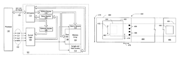
- FIG. 1 is a simplified block diagram of a memory device coupled to a processor as part of an electronic system, according to an embodiment of the disclosure.
- FIG. 2 is a schematic of a portion of an example NAND memory array as might be found in the memory device of FIG. 1 .
- FIG. 3 is a block diagram of additional detail of a row decode circuitry and a memory array as might be found in the memory device of FIG. 1 .
- FIGS. 4A-4B are top and side views of a transistor in accordance with an embodiment of the disclosure.
- Embodiments described herein include transistors for use in semiconductor integrated circuit devices.
- the transistors include a donut-shaped channel region, such that one source/drain region of the transistor is formed around a perimeter of the channel region, and the other source/drain region is formed to extend through the channel region such that the channel region is formed around a perimeter of an upper portion of the other source/drain region.
- Such transistors should facilitate a reduction in edge effect and leakage as the channel of the transistor is not bordering on an isolation region.
- the use of a source/drain region extending through the channel region facilitates high-power, high-voltage operation.
- FIG. 1 is a simplified block diagram of a memory device 100 , as one example of an integrated circuit device, in communication with (e.g., coupled to) a processor 130 as part of an electronic system, according to an embodiment of the disclosure.
- electronic systems include personal computers, personal digital assistants (PDAs), digital cameras, digital media players, digital recorders, games, appliances, vehicles, wireless devices, cellular telephones and the like.
- the processor 130 may be a memory controller or other external processor.
- Memory device 100 includes an array of memory cells 104 logically arranged in rows and columns. Although various embodiments will be described primarily with reference to NAND memory arrays, the various embodiments are not limited to a specific architecture of the memory array 104 . Some examples of other array architectures suitable for the present embodiments include NOR arrays, AND arrays or other arrays.
- a row decode circuitry 108 and a column decode circuitry 110 are provided to decode address signals.
- Row decode circuitry 108 contains one or more transistors in accordance with embodiments of the disclosure.
- Address signals are received and decoded to access memory array 104 .
- Memory device 100 also includes input/output (I/O) control circuitry 112 to manage input of commands, addresses and data to the memory device 100 as well as output of data and status information from the memory device 100 .
- An address register 114 is coupled between I/O control circuitry 112 and row decode circuitry 108 and column decode circuitry 110 to latch the address signals prior to decoding.
- a command register 124 is coupled between I/O control circuitry 112 and control logic 116 to latch incoming commands.
- Control logic 116 is also coupled to a cache register 118 .
- Cache register 118 latches data, either incoming or outgoing, as directed by control logic 116 to temporarily store data while the memory array 104 is busy writing or reading, respectively, other data.
- data is passed from the cache register 118 to data register 120 for transfer to the memory array 104 ; then new data is latched in the cache register 118 from the I/O control circuitry 112 .
- During a read operation data is passed from the cache register 118 to the I/O control circuitry 112 for output to the external processor 130 ; then new data is passed from the data register 120 to the cache register 118 .
- a status register 122 is coupled between I/O control circuitry 112 and control logic 116 to latch the status information for output to the processor 130 .
- Memory device 100 receives control signals at control logic 116 from processor 130 over a control link 132 .
- the control signals may include a chip enable CE#, a command latch enable CLE, an address latch enable ALE, and a write enable WE#.
- Memory device 100 receives commands (in the form of command signals), addresses (in the form of address signals), and data (in the form of data signals) from processor 130 over a multiplexed input/output (I/O) bus 134 and outputs data to processor 130 over I/O bus 134 .
- I/O input/output
- the commands are received over input/output (I/O) pins [7:0] of I/O bus 134 at I/O control circuitry 112 and are written into command register 124 .
- the addresses are received over input/output (I/O) pins [7:0] of bus 134 at I/O control circuitry 112 and are written into address register 114 .
- the data are received over input/output (I/O) pins [7:0] for an 8-bit device or input/output (I/O) pins [15:0] for a 16-bit device at I/O control circuitry 112 and are written into cache register 118 .
- the data are subsequently written into data register 120 for programming memory array 104 .
- cache register 118 may be omitted, and the data are written directly into data register 120 .
- Data are also output over input/output (I/O) pins [7:0] for an 8-bit device or input/output (I/O) pins [15:0] for a 16-bit device.
- I/O input/output
- FIG. 1 has been simplified to help focus on the present disclosure. Additionally, while the memory device of FIG. 1 has been described in accordance with popular conventions for receipt and output of the various signals, it is noted that the various embodiments are not limited by the specific signals and I/O configurations described unless expressly noted herein.
- FIG. 2 is a schematic of a portion of an example NAND memory array 200 as might be found in the memory array 104 of FIG. 1 .
- the memory array 200 includes access lines, commonly referred to as word lines (which may comprise commonly coupled control gates 202 1 to 202 N ) and intersecting data lines, such as bit lines 204 1 to 204 M .
- word lines which may comprise commonly coupled control gates 202 1 to 202 N
- bit lines 204 1 to 204 M intersecting data lines
- the number of word lines 202 and the number of bit lines 204 are generally each some power of two.
- Memory array 200 includes NAND strings 206 1 to 206 M .
- Each NAND string includes transistors 208 1 to 208 N , each located at an intersection of a word line 202 and a bit line 204 .
- the transistors 208 depicted as floating-gate transistors in FIG. 2 , represent non-volatile memory cells for storage of data.
- the floating-gate transistors 208 of each NAND string 206 are connected in series source to drain between one or more source select gates 210 , e.g., a field-effect transistor (FET), and one or more drain select gates 212 , e.g., an FET.
- Each source select gate 210 is located at an intersection of a local bit line 204 and a source select line 214
- each drain select gate 212 is located at an intersection of a local bit line 204 and a drain select line 215 .
- a source of each source select gate 210 is connected to a common source line 216 .
- the drain of each source select gate 210 is connected to the source of the first floating-gate transistor 208 of the corresponding NAND string 206 .
- the drain of source select gate 210 1 is connected to the source of floating-gate transistor 208 1 of the corresponding NAND string 206 1 .
- a control gate of each source select gate 210 is connected to source select line 214 . If multiple source select gates 210 are utilized for a given NAND string 206 , they would be coupled in series between the common source line 216 and the first floating-gate transistor 208 of that NAND string 206 .
- each drain select gate 212 is connected to a local bit line 204 for the corresponding NAND string at a drain contact.
- the drain of drain select gate 212 1 is connected to the local bit line 204 1 for the corresponding NAND string 206 1 at a drain contact.
- the source of each drain select gate 212 is connected to the drain of the last floating-gate transistor 208 of the corresponding NAND string 206 .
- the source of drain select gate 212 1 is connected to the drain of floating-gate transistor 208 N of the corresponding NAND string 206 1 . If multiple drain select gates 212 are utilized for a given NAND string 206 , they would be coupled in series between the corresponding bit line 204 and the last floating-gate transistor 208 N of that NAND string 206 .
- FIG. 3 is a block diagram of additional detail of a row decode circuitry 108 and a memory array 104 as might be found in the memory device 100 of FIG. 1 .
- FIG. 3 depicts n+1 blocks of memory cells 348 . Referring to a memory array of the type depicted in FIG. 2 , a block of memory cells 348 would generally be all of the NAND strings 206 commonly coupled to the same word lines 202 . However, other numbers of blocks of memory cells 348 or other groupings of memory cells could be used.
- FIG. 3 further depicts 32 word lines, i.e., WL 0 -WL 31 . Again, other numbers of word lines could be used with various embodiments.
- Each of the blocks of memory cells 348 is associated with a word line driver 344 and a block decoder 342 .
- Block decoders 342 are responsive to control signals from the control logic 116 to selectively activate their respective word line drivers 344 .
- Each word line driver 344 is coupled to the word lines of their respective block of memory cells 348 .
- Each word line driver 344 is further coupled to a global word line driver 346 .
- Global word line driver 346 is adapted to supply the potentials for driving the word lines of the block of memory cells 348 through its respective word line driver 344 that has been activated by its respective block decoder 342 .
- the word line drivers 344 contain transistors (not shown in FIG.
- FIGS. 4A-4B are top and side views of a transistor 450 in accordance with an embodiment of the disclosure.
- Transistor 450 includes a control gate 452 , and a gate dielectric 454 formed between a semiconductor material 458 and the control gate 452 .
- the control gate 452 is coupled to receive a control signal from a block decoder (not shown in FIGS. 4A-4B ).
- the semiconductor material 458 is a semiconductor material or materials of a first conductivity type, such as a p-type monocrystalline silicon substrate, for example.
- the control gate 452 is a conductor and may include one or more layers of conductive material.
- the control gate 452 may include conductively-doped polysilicon, metals, metal silicides and other conductive materials.
- the gate dielectric 454 is a dielectric material.
- the gate dielectric 454 may include thermally-grown silicon dioxide (SiO 2 ) on a silicon semiconductor material 458 .
- the gate dielectric 454 may further include dielectrics of higher K values, such as hafnium oxide (HfO 2 ), zirconium oxide (ZrO 2 ), aluminum oxide (Al 2 O 3 ), aluminum hafnium oxide (AlHfOx), etc.
- HfO 2 hafnium oxide
- ZrO 2 zirconium oxide
- Al 2 O 3 aluminum oxide
- AlHfOx aluminum hafnium oxide
- the transistor 450 further includes a channel region 456 formed in the semiconductor material 458 below the gate dielectric 454 .
- the channel region 456 has the first conductivity type and may include doping of the semiconductor material 458 to increase its conductivity.
- the semiconductor material 458 is a p-type monocrystalline silicon
- the channel region 456 could include increasing the p-type conductivity through doping using boron (B) or another p-type impurity.
- the transistor 450 further includes a source/drain region 462 formed in the semiconductor material 458 and passing through the channel region 456 , such that the channel region 456 is formed around a perimeter of the source/drain region 462 .
- the source/drain region 462 has a conductivity type different than the first conductivity type, i.e., a second conductivity type.
- the second conductivity type is an opposite conductivity type from the first conductivity type.
- the source/drain region 462 could include an n-type region formed in the semiconductor material 458 , such as by doping with antimony (Sb), arsenic (As), phosphorus (P) or another n-type impurity.
- the source/drain region 462 is coupled to a well region 464 .
- the well region 464 has the second conductivity type and is formed in the semiconductor material 458 below a level of the channel region 456 . Formation of the well region 464 could include a deep implant of n-type impurities, in this example.
- the well region 464 is coupled to a contact 466 that is coupled to receive a potential from a global word line driver (not shown in FIGS. 4A-4B ).
- Contact 466 may be include a conductive region having the second conductivity type.
- Contact 466 is laterally spaced apart from the source/drain region 462 and extends into the semiconductor material 458 to at least a level of the well region 464 , thereby coupling the contact 466 to the source/drain region 462 through the well region 464 .
- a global word line driver such as global word line driver 346
- one or more local word line drivers such as word line drivers 344
- metal levels running tangentially to the word lines may be reduced or eliminated compared to devices relying on interconnects formed above a surface of the semiconductor material 458 .
- the transistor 450 further includes a source/drain region 460 formed in the semiconductor material 458 around a perimeter of the channel region 456 .
- the source/drain region 460 has the second conductivity type.
- One or more contacts 468 are coupled to the source/drain region 460 and to a word line (not shown in FIGS. 4A-4B ). In this manner, activation of the transistor 450 couples a potential from a global word line driver to its associated word line.
- Example dimensions of transistor 450 within the capabilities of common fabrication techniques currently employed include a width 472 of the source/drain region 462 of less than or equal to 1 ⁇ m.
- a width 470 of the source/drain region 460 might be less than or equal to 2 ⁇ m
- a distance 474 between a perimeter of the source/drain region 462 and a perimeter of the channel region 456 might be less than or equal to 0.5 ⁇ m.
- a distance 476 between a perimeter of the channel region 456 and the word line contacts 468 might be less than 0.5 ⁇ m.
- the transistor 450 is depicted to contain substantially square features, one or more of the control gate 452 , the gate dielectric 454 , the source/drain region 460 , the channel region 456 and the source/drain region 462 may include circular features or some other geometric shape. Each would be deemed a donut-shaped channel region 456 , as that term is used herein, as there would be a hole in the interior of the channel region 456 , and the channel region 456 would have an interior periphery adjacent source/drain region 462 and an exterior periphery adjacent source/drain region 460 .
- Block decoder 342 1 receives a control signal from the control logic 116 indicative of a desire to select the block of memory cells 348 1 .
- block decoder 342 1 applies a potential to the control gate 452 of the transistor 450 sufficient to activate the transistor 450 .
- the global word line driver 346 receives a control signal from the control logic 116 indicative of a desire to supply word line potentials to the memory array 104 .
- the global word line driver 346 applies a particular potential to the well region 464 and thus to the source/drain region 462 .
- different word line potentials are applied to different word lines of a block of memory cells 348 , depending upon their relationship to a target word line, although the disclosure is not limited by any particular word line potentials.
Abstract
Description
Claims (23)
Priority Applications (1)
| Application Number | Priority Date | Filing Date | Title |
|---|---|---|---|
| US12/476,681 US8102709B2 (en) | 2009-06-02 | 2009-06-02 | Transistor having peripheral channel |
Applications Claiming Priority (1)
| Application Number | Priority Date | Filing Date | Title |
|---|---|---|---|
| US12/476,681 US8102709B2 (en) | 2009-06-02 | 2009-06-02 | Transistor having peripheral channel |
Publications (2)
| Publication Number | Publication Date |
|---|---|
| US20100302848A1 US20100302848A1 (en) | 2010-12-02 |
| US8102709B2 true US8102709B2 (en) | 2012-01-24 |
Family
ID=43220043
Family Applications (1)
| Application Number | Title | Priority Date | Filing Date |
|---|---|---|---|
| US12/476,681 Active 2030-07-24 US8102709B2 (en) | 2009-06-02 | 2009-06-02 | Transistor having peripheral channel |
Country Status (1)
| Country | Link |
|---|---|
| US (1) | US8102709B2 (en) |
Cited By (1)
| Publication number | Priority date | Publication date | Assignee | Title |
|---|---|---|---|---|
| US11751386B2 (en) | 2021-08-11 | 2023-09-05 | Micron Technology, Inc. | Field-effect transistors, devices containing such field-effect transistors and methods of their formation |
Families Citing this family (6)
| Publication number | Priority date | Publication date | Assignee | Title |
|---|---|---|---|---|
| US9190144B2 (en) * | 2012-10-12 | 2015-11-17 | Micron Technology, Inc. | Memory device architecture |
| US10748931B2 (en) | 2018-05-08 | 2020-08-18 | Micron Technology, Inc. | Integrated assemblies having ferroelectric transistors with body regions coupled to carrier reservoirs |
| CN113454779A (en) | 2019-03-06 | 2021-09-28 | 美光科技公司 | An integrated assembly having a transistor body region coupled to a carrier trench structure; and method of forming an integrated assembly |
| CN115769693A (en) * | 2021-06-30 | 2023-03-07 | 长江存储科技有限责任公司 | Three-dimensional memory device and method of forming the same |
| KR20230101921A (en) | 2021-06-30 | 2023-07-06 | 양쯔 메모리 테크놀로지스 씨오., 엘티디. | Three-dimensional memory device and method for forming the same |
| WO2023024342A1 (en) * | 2021-08-23 | 2023-03-02 | Yangtze Memory Technologies Co., Ltd. | Three-dimensional memory devices and methods for forming the same |
Citations (10)
| Publication number | Priority date | Publication date | Assignee | Title |
|---|---|---|---|---|
| EP0880183A2 (en) | 1997-05-23 | 1998-11-25 | Texas Instruments Incorporated | LDMOS power device |
| US5910925A (en) * | 1992-01-14 | 1999-06-08 | Sandisk Corporation | EEPROM with split gate source side injection |
| US6009017A (en) * | 1998-03-13 | 1999-12-28 | Macronix International Co., Ltd. | Floating gate memory with substrate band-to-band tunneling induced hot electron injection |
| US20030161192A1 (en) * | 2000-09-12 | 2003-08-28 | Toshio Kobayashi | Nonvolatile semiconductor memory device and methods for operating and producing the same |
| US20040004863A1 (en) * | 2002-07-05 | 2004-01-08 | Chih-Hsin Wang | Nonvolatile electrically alterable memory device and array made thereby |
| US20040233726A1 (en) * | 2003-05-20 | 2004-11-25 | Yasuaki Iwase | Programming verification method of nonvolatile memory cell, semiconductor memory device, and portable electronic apparatus having the semiconductor memory device |
| US20040257875A1 (en) * | 2003-05-16 | 2004-12-23 | Yoshifumi Yaoi | Semiconductor memory device and portable electronic apparatus |
| US20050243601A1 (en) * | 1988-06-08 | 2005-11-03 | Eliyahou Harari | Highly compact Eprom and flash EEprom devices |
| US7050330B2 (en) * | 2003-12-16 | 2006-05-23 | Micron Technology, Inc. | Multi-state NROM device |
| US20070183213A1 (en) * | 2006-02-03 | 2007-08-09 | Renesas Technology Corp. | Nonvolatile semiconductor memory device |
-
2009
- 2009-06-02 US US12/476,681 patent/US8102709B2/en active Active
Patent Citations (10)
| Publication number | Priority date | Publication date | Assignee | Title |
|---|---|---|---|---|
| US20050243601A1 (en) * | 1988-06-08 | 2005-11-03 | Eliyahou Harari | Highly compact Eprom and flash EEprom devices |
| US5910925A (en) * | 1992-01-14 | 1999-06-08 | Sandisk Corporation | EEPROM with split gate source side injection |
| EP0880183A2 (en) | 1997-05-23 | 1998-11-25 | Texas Instruments Incorporated | LDMOS power device |
| US6009017A (en) * | 1998-03-13 | 1999-12-28 | Macronix International Co., Ltd. | Floating gate memory with substrate band-to-band tunneling induced hot electron injection |
| US20030161192A1 (en) * | 2000-09-12 | 2003-08-28 | Toshio Kobayashi | Nonvolatile semiconductor memory device and methods for operating and producing the same |
| US20040004863A1 (en) * | 2002-07-05 | 2004-01-08 | Chih-Hsin Wang | Nonvolatile electrically alterable memory device and array made thereby |
| US20040257875A1 (en) * | 2003-05-16 | 2004-12-23 | Yoshifumi Yaoi | Semiconductor memory device and portable electronic apparatus |
| US20040233726A1 (en) * | 2003-05-20 | 2004-11-25 | Yasuaki Iwase | Programming verification method of nonvolatile memory cell, semiconductor memory device, and portable electronic apparatus having the semiconductor memory device |
| US7050330B2 (en) * | 2003-12-16 | 2006-05-23 | Micron Technology, Inc. | Multi-state NROM device |
| US20070183213A1 (en) * | 2006-02-03 | 2007-08-09 | Renesas Technology Corp. | Nonvolatile semiconductor memory device |
Non-Patent Citations (1)
| Title |
|---|
| SHF products for 10-100G "LDMOS" updated Jun. 17, 2006, 3 pages, Microwave Encyclopedia-www.Microwaves101.com. |
Cited By (1)
| Publication number | Priority date | Publication date | Assignee | Title |
|---|---|---|---|---|
| US11751386B2 (en) | 2021-08-11 | 2023-09-05 | Micron Technology, Inc. | Field-effect transistors, devices containing such field-effect transistors and methods of their formation |
Also Published As
| Publication number | Publication date |
|---|---|
| US20100302848A1 (en) | 2010-12-02 |
Similar Documents
| Publication | Publication Date | Title |
|---|---|---|
| US10354730B2 (en) | Multi-deck memory device with access line and data line segregation between decks and method of operation thereof | |
| JP7112411B2 (en) | Multi-gate induced drain leakage current generator | |
| US20230420049A1 (en) | 3d memory device including shared select gate connections between memory blocks | |
| US8102709B2 (en) | Transistor having peripheral channel | |
| US7551491B2 (en) | Unit cell of a non-volatile memory device, a non-volatile memory device and method thereof | |
| US11069408B2 (en) | Apparatus for discharging control gates after performing an access operation on a memory cell | |
| KR20210070219A (en) | Apparatus and methods for seeding operations concurrently with data line set operations | |
| US11335675B2 (en) | Circuit-protection devices | |
| US11848060B2 (en) | Memory devices with dynamic program verify levels | |
| WO2021041029A1 (en) | Erasing memory | |
| US20220301634A1 (en) | Memory device read operations | |
| WO2018076239A1 (en) | Erasing memory cells | |
| US11869590B2 (en) | Memory devices including gate leakage transistors | |
| US11081165B2 (en) | Memories for decoding memory access addresses for access operations | |
| US11562799B2 (en) | Memory devices for program verify operations | |
| US11545220B2 (en) | Split-gate memory cells | |
| US20240071531A1 (en) | Memory devices with program verify levels based on compensation values |
Legal Events
| Date | Code | Title | Description |
|---|---|---|---|
| AS | Assignment |
Owner name: MICRON TECHNOLOGY, INC., IDAHO Free format text: ASSIGNMENT OF ASSIGNORS INTEREST;ASSIGNOR:MIKHALEV, VLADIMIR;REEL/FRAME:022767/0590 Effective date: 20090529 |
|
| FEPP | Fee payment procedure |
Free format text: PAYOR NUMBER ASSIGNED (ORIGINAL EVENT CODE: ASPN); ENTITY STATUS OF PATENT OWNER: LARGE ENTITY |
|
| STCF | Information on status: patent grant |
Free format text: PATENTED CASE |
|
| FPAY | Fee payment |
Year of fee payment: 4 |
|
| AS | Assignment |
Owner name: U.S. BANK NATIONAL ASSOCIATION, AS COLLATERAL AGENT, CALIFORNIA Free format text: SECURITY INTEREST;ASSIGNOR:MICRON TECHNOLOGY, INC.;REEL/FRAME:038669/0001 Effective date: 20160426 Owner name: U.S. BANK NATIONAL ASSOCIATION, AS COLLATERAL AGEN Free format text: SECURITY INTEREST;ASSIGNOR:MICRON TECHNOLOGY, INC.;REEL/FRAME:038669/0001 Effective date: 20160426 |
|
| AS | Assignment |
Owner name: MORGAN STANLEY SENIOR FUNDING, INC., AS COLLATERAL AGENT, MARYLAND Free format text: PATENT SECURITY AGREEMENT;ASSIGNOR:MICRON TECHNOLOGY, INC.;REEL/FRAME:038954/0001 Effective date: 20160426 Owner name: MORGAN STANLEY SENIOR FUNDING, INC., AS COLLATERAL Free format text: PATENT SECURITY AGREEMENT;ASSIGNOR:MICRON TECHNOLOGY, INC.;REEL/FRAME:038954/0001 Effective date: 20160426 |
|
| AS | Assignment |
Owner name: U.S. BANK NATIONAL ASSOCIATION, AS COLLATERAL AGENT, CALIFORNIA Free format text: CORRECTIVE ASSIGNMENT TO CORRECT THE REPLACE ERRONEOUSLY FILED PATENT #7358718 WITH THE CORRECT PATENT #7358178 PREVIOUSLY RECORDED ON REEL 038669 FRAME 0001. ASSIGNOR(S) HEREBY CONFIRMS THE SECURITY INTEREST;ASSIGNOR:MICRON TECHNOLOGY, INC.;REEL/FRAME:043079/0001 Effective date: 20160426 Owner name: U.S. BANK NATIONAL ASSOCIATION, AS COLLATERAL AGEN Free format text: CORRECTIVE ASSIGNMENT TO CORRECT THE REPLACE ERRONEOUSLY FILED PATENT #7358718 WITH THE CORRECT PATENT #7358178 PREVIOUSLY RECORDED ON REEL 038669 FRAME 0001. ASSIGNOR(S) HEREBY CONFIRMS THE SECURITY INTEREST;ASSIGNOR:MICRON TECHNOLOGY, INC.;REEL/FRAME:043079/0001 Effective date: 20160426 |
|
| AS | Assignment |
Owner name: JPMORGAN CHASE BANK, N.A., AS COLLATERAL AGENT, ILLINOIS Free format text: SECURITY INTEREST;ASSIGNORS:MICRON TECHNOLOGY, INC.;MICRON SEMICONDUCTOR PRODUCTS, INC.;REEL/FRAME:047540/0001 Effective date: 20180703 Owner name: JPMORGAN CHASE BANK, N.A., AS COLLATERAL AGENT, IL Free format text: SECURITY INTEREST;ASSIGNORS:MICRON TECHNOLOGY, INC.;MICRON SEMICONDUCTOR PRODUCTS, INC.;REEL/FRAME:047540/0001 Effective date: 20180703 |
|
| AS | Assignment |
Owner name: MICRON TECHNOLOGY, INC., IDAHO Free format text: RELEASE BY SECURED PARTY;ASSIGNOR:U.S. BANK NATIONAL ASSOCIATION, AS COLLATERAL AGENT;REEL/FRAME:047243/0001 Effective date: 20180629 |
|
| MAFP | Maintenance fee payment |
Free format text: PAYMENT OF MAINTENANCE FEE, 8TH YEAR, LARGE ENTITY (ORIGINAL EVENT CODE: M1552); ENTITY STATUS OF PATENT OWNER: LARGE ENTITY Year of fee payment: 8 |
|
| AS | Assignment |
Owner name: MICRON TECHNOLOGY, INC., IDAHO Free format text: RELEASE BY SECURED PARTY;ASSIGNOR:MORGAN STANLEY SENIOR FUNDING, INC., AS COLLATERAL AGENT;REEL/FRAME:050937/0001 Effective date: 20190731 |
|
| AS | Assignment |
Owner name: MICRON SEMICONDUCTOR PRODUCTS, INC., IDAHO Free format text: RELEASE BY SECURED PARTY;ASSIGNOR:JPMORGAN CHASE BANK, N.A., AS COLLATERAL AGENT;REEL/FRAME:051028/0001 Effective date: 20190731 Owner name: MICRON TECHNOLOGY, INC., IDAHO Free format text: RELEASE BY SECURED PARTY;ASSIGNOR:JPMORGAN CHASE BANK, N.A., AS COLLATERAL AGENT;REEL/FRAME:051028/0001 Effective date: 20190731 |
|
| MAFP | Maintenance fee payment |
Free format text: PAYMENT OF MAINTENANCE FEE, 12TH YEAR, LARGE ENTITY (ORIGINAL EVENT CODE: M1553); ENTITY STATUS OF PATENT OWNER: LARGE ENTITY Year of fee payment: 12 |