US8119509B2 - Method of manufacturing high-integrated semiconductor device and semiconductor device manufactured using the same - Google Patents
Method of manufacturing high-integrated semiconductor device and semiconductor device manufactured using the same Download PDFInfo
- Publication number
- US8119509B2 US8119509B2 US12/495,554 US49555409A US8119509B2 US 8119509 B2 US8119509 B2 US 8119509B2 US 49555409 A US49555409 A US 49555409A US 8119509 B2 US8119509 B2 US 8119509B2
- Authority
- US
- United States
- Prior art keywords
- layer
- metal layer
- forming
- etching
- silicon pillars
- Prior art date
- Legal status (The legal status is an assumption and is not a legal conclusion. Google has not performed a legal analysis and makes no representation as to the accuracy of the status listed.)
- Expired - Fee Related, expires
Links
- 239000004065 semiconductor Substances 0.000 title claims abstract description 83
- 238000004519 manufacturing process Methods 0.000 title claims description 14
- 239000002184 metal Substances 0.000 claims abstract description 75
- XUIMIQQOPSSXEZ-UHFFFAOYSA-N Silicon Chemical compound [Si] XUIMIQQOPSSXEZ-UHFFFAOYSA-N 0.000 claims description 85
- 229910052710 silicon Inorganic materials 0.000 claims description 85
- 239000010703 silicon Substances 0.000 claims description 85
- 238000000034 method Methods 0.000 claims description 65
- 230000008569 process Effects 0.000 claims description 52
- 238000005530 etching Methods 0.000 claims description 37
- 239000000758 substrate Substances 0.000 claims description 37
- 238000000151 deposition Methods 0.000 claims description 10
- 238000005245 sintering Methods 0.000 claims description 5
- 238000006884 silylation reaction Methods 0.000 claims description 4
- 230000004888 barrier function Effects 0.000 abstract description 28
- 239000010410 layer Substances 0.000 description 200
- 229920002120 photoresistant polymer Polymers 0.000 description 47
- 239000011229 interlayer Substances 0.000 description 35
- 125000006850 spacer group Chemical group 0.000 description 18
- 239000004020 conductor Substances 0.000 description 11
- 150000004767 nitrides Chemical class 0.000 description 10
- 238000000206 photolithography Methods 0.000 description 9
- 238000005468 ion implantation Methods 0.000 description 8
- 238000007517 polishing process Methods 0.000 description 7
- 239000003990 capacitor Substances 0.000 description 4
- 238000000059 patterning Methods 0.000 description 4
- 238000000137 annealing Methods 0.000 description 3
- 239000012535 impurity Substances 0.000 description 3
- 238000007792 addition Methods 0.000 description 2
- 239000011248 coating agent Substances 0.000 description 2
- 238000000576 coating method Methods 0.000 description 2
- 239000000615 nonconductor Substances 0.000 description 2
- 230000004044 response Effects 0.000 description 2
- 238000003860 storage Methods 0.000 description 2
- 230000008901 benefit Effects 0.000 description 1
- 230000015572 biosynthetic process Effects 0.000 description 1
- 230000002950 deficient Effects 0.000 description 1
- 238000010292 electrical insulation Methods 0.000 description 1
- 230000010354 integration Effects 0.000 description 1
- 230000000873 masking effect Effects 0.000 description 1
- 239000000463 material Substances 0.000 description 1
- 239000007769 metal material Substances 0.000 description 1
- 238000012986 modification Methods 0.000 description 1
- 230000004048 modification Effects 0.000 description 1
- 230000002093 peripheral effect Effects 0.000 description 1
- 238000005498 polishing Methods 0.000 description 1
- 239000000126 substance Substances 0.000 description 1
Images


Classifications
-
- H—ELECTRICITY
- H01—ELECTRIC ELEMENTS
- H01L—SEMICONDUCTOR DEVICES NOT COVERED BY CLASS H10
- H01L21/00—Processes or apparatus adapted for the manufacture or treatment of semiconductor or solid state devices or of parts thereof
- H01L21/02—Manufacture or treatment of semiconductor devices or of parts thereof
- H01L21/04—Manufacture or treatment of semiconductor devices or of parts thereof the devices having at least one potential-jump barrier or surface barrier, e.g. PN junction, depletion layer or carrier concentration layer
- H01L21/18—Manufacture or treatment of semiconductor devices or of parts thereof the devices having at least one potential-jump barrier or surface barrier, e.g. PN junction, depletion layer or carrier concentration layer the devices having semiconductor bodies comprising elements of Group IV of the Periodic System or AIIIBV compounds with or without impurities, e.g. doping materials
-
- H—ELECTRICITY
- H01—ELECTRIC ELEMENTS
- H01L—SEMICONDUCTOR DEVICES NOT COVERED BY CLASS H10
- H01L29/00—Semiconductor devices adapted for rectifying, amplifying, oscillating or switching, or capacitors or resistors with at least one potential-jump barrier or surface barrier, e.g. PN junction depletion layer or carrier concentration layer; Details of semiconductor bodies or of electrodes thereof ; Multistep manufacturing processes therefor
- H01L29/66—Types of semiconductor device ; Multistep manufacturing processes therefor
- H01L29/66007—Multistep manufacturing processes
- H01L29/66075—Multistep manufacturing processes of devices having semiconductor bodies comprising group 14 or group 13/15 materials
- H01L29/66227—Multistep manufacturing processes of devices having semiconductor bodies comprising group 14 or group 13/15 materials the devices being controllable only by the electric current supplied or the electric potential applied, to an electrode which does not carry the current to be rectified, amplified or switched, e.g. three-terminal devices
- H01L29/66409—Unipolar field-effect transistors
- H01L29/66477—Unipolar field-effect transistors with an insulated gate, i.e. MISFET
- H01L29/66666—Vertical transistors
-
- H—ELECTRICITY
- H01—ELECTRIC ELEMENTS
- H01L—SEMICONDUCTOR DEVICES NOT COVERED BY CLASS H10
- H01L21/00—Processes or apparatus adapted for the manufacture or treatment of semiconductor or solid state devices or of parts thereof
- H01L21/02—Manufacture or treatment of semiconductor devices or of parts thereof
- H01L21/04—Manufacture or treatment of semiconductor devices or of parts thereof the devices having at least one potential-jump barrier or surface barrier, e.g. PN junction, depletion layer or carrier concentration layer
- H01L21/18—Manufacture or treatment of semiconductor devices or of parts thereof the devices having at least one potential-jump barrier or surface barrier, e.g. PN junction, depletion layer or carrier concentration layer the devices having semiconductor bodies comprising elements of Group IV of the Periodic System or AIIIBV compounds with or without impurities, e.g. doping materials
- H01L21/28—Manufacture of electrodes on semiconductor bodies using processes or apparatus not provided for in groups H01L21/20 - H01L21/268
-
- H—ELECTRICITY
- H01—ELECTRIC ELEMENTS
- H01L—SEMICONDUCTOR DEVICES NOT COVERED BY CLASS H10
- H01L29/00—Semiconductor devices adapted for rectifying, amplifying, oscillating or switching, or capacitors or resistors with at least one potential-jump barrier or surface barrier, e.g. PN junction depletion layer or carrier concentration layer; Details of semiconductor bodies or of electrodes thereof ; Multistep manufacturing processes therefor
- H01L29/66—Types of semiconductor device ; Multistep manufacturing processes therefor
- H01L29/68—Types of semiconductor device ; Multistep manufacturing processes therefor controllable by only the electric current supplied, or only the electric potential applied, to an electrode which does not carry the current to be rectified, amplified or switched
- H01L29/76—Unipolar devices, e.g. field effect transistors
- H01L29/772—Field effect transistors
- H01L29/78—Field effect transistors with field effect produced by an insulated gate
- H01L29/7827—Vertical transistors
-
- H—ELECTRICITY
- H10—SEMICONDUCTOR DEVICES; ELECTRIC SOLID-STATE DEVICES NOT OTHERWISE PROVIDED FOR
- H10B—ELECTRONIC MEMORY DEVICES
- H10B12/00—Dynamic random access memory [DRAM] devices
- H10B12/01—Manufacture or treatment
- H10B12/02—Manufacture or treatment for one transistor one-capacitor [1T-1C] memory cells
- H10B12/05—Making the transistor
- H10B12/053—Making the transistor the transistor being at least partially in a trench in the substrate
Definitions
- the present invention relates to a method of manufacturing a semiconductor device and, more particularly, to a method of manufacturing a highly integrated semiconductor device (e.g., vertical transistors) and improving the operating characteristic and yield of the semiconductor device.
- a highly integrated semiconductor device e.g., vertical transistors
- a semiconductor is a material classified according to its electrical conductivity and belongs to an intermediate region between a conductor and a nonconductor.
- the semiconductor has a property that is similar to that of the nonconductor in a pure state, but has an increasing electrical conductivity with the addition of impurities or other control.
- Such a semiconductor is used to produce semiconductor elements, such as transistors, by adding impurities and connecting conductors thereto.
- a device fabricated using the semiconductor elements and configured to have a variety of functions is called a semiconductor device.
- a representative example of the semiconductor device may include a semiconductor memory device.
- the semiconductor memory device includes a number of unit cells each comprising a capacitor and a transistor.
- the capacitor is used to temporarily store data.
- the transistor is used to transfer data between a bit line and the capacitor in response to a control signal (a word line).
- the transistor is divided into three regions; a gate, a source, and a drain. Electric charges are moved between the source and the drain in response to the control signal input to the gate. The movement of electric charges between the source and the drain is carried out through a channel region.
- a gate is formed in the semiconductor substrate, and a source and a drain are formed on both sides of the gate by doping impurities.
- a channel region of the transistor is formed between the source and the drain under the gate.
- the transistor having this horizontal channel region occupies a certain area of the semiconductor substrate. Accordingly, in the case where a complicated semiconductor memory device is fabricated, it is difficult to reduce the area of the semiconductor memory device because of a number of transistors included in the semiconductor memory device.
- productivity can be improved because the number of semiconductor memory devices that can be produced per wafer can be increased.
- Several methods are being proposed in order to reduce the area of the semiconductor memory device.
- One of the methods is to use a vertical transistor having a vertical channel region instead of a conventional horizontal transistor having a horizontal channel region.
- Various embodiments of the invention are directed to providing a method of manufacturing a semiconductor device including vertical transistors, which is capable of improving the operating characteristic and yield of a semiconductor device by forming bit lines using a conductive material and removing alignment error when the bit lines are formed, and a semiconductor device manufactured using the same.
- a semiconductor device comprises a plurality of vertical transistors each comprising barrier metal layers corresponding to source/drain regions in which a conduction region is formed under a channel region having a pillar form, and a bit line comprising a metal layer to connect the plurality of vertical transistors.
- the barrier metal layers are formed in parallel in a direction of the bit lines under the channel region.
- the barrier metal layers and the metal layer are made of a same metal material.
- each of the vertical transistors further comprises the channel region having the pillar form, a gate oxide layer to surround the channel region, and a gate electrode to surround sidewalls of the gate oxide layer.
- the gate electrode is coupled to a gate electrode of a neighboring vertical transistor by a word line, and the word line is formed over the word line in a direction crossing the bit lines.
- a method of manufacturing a semiconductor memory device comprises forming barrier metal layers on lower sides of each of silicon pillars coupled by a bit line, and forming gate electrodes on sidewalls of each of the silicon pillars, thereby completing a vertical transistor.
- the forming-a-barrier-metal-layer-on-lower-sides-of-silicon-pillars-coupled-by-a-bit-line includes forming silicon line patterns in a first direction by etching a semiconductor substrate, forming metal layers each between the silicon line patterns, a first insulating layer on the metal layers, forming the silicon pillars by isotropically etching the silicon line patterns in a second direction to cross the first direction, and forming the barrier metal layers on the lower sides of each of the silicon pillars, thereby completing the bit lines.
- the forming silicon-line-patterns-in-a-first-direction-by-etching-a-semiconductor-substrate includes forming a mask layer over the semiconductor substrate and patterning the mask layer by performing a photolithography process, forming first patterns by etching the semiconductor substrate using the patterned mask layer, and forming a spacer on sidewalls of each of the first patterns and etching the semiconductor substrate using the patterned mask layer and the spacers as an etch mask.
- the forming-a-mask-layer-over-the-semiconductor-substrate-and-patterning-the-mask-layer-by-performing-a-photolithography-process includes forming a pad oxide layer on the semiconductor substrate, forming a hard mask layer on the pad oxide layer, coating a photoresist layer on the hard mask layer and patterning the photoresist layer using a photolithography process, etching an exposed hard mask layer using the patterned photoresist layer as an etch mask, and etching the exposed pad oxide layer using the etched hard mask layer.
- the forming-a-metal-layer-between-the-silicon-line-patterns includes depositing the metal layer between the silicon line patterns, and etching back the metal layer to expose all the spacers.
- the forming-the-silicon-pillars-by-isotropicly-etching-the-silicon-line-patterns-in-a-second-direction-to-cross-the-first-direction includes forming the mask layer on the first insulating layer and patterning the mask layer having a line form of the second direction crossing the first direction by performing a photolithography process, forming second patterns by etching the first insulating layer and the semiconductor substrate using the patterned mask layer, and forming spacers on sidewalls of each of the second patterns and isotropically etching the semiconductor substrate using the patterned mask layer and the spacers as an etch mask.
- the forming-the-barrier-metal-layers-on-the-lower-sides-of-each-of-the-silicon-pillars-thereby-completing-the-bit-lines includes depositing a barrier metal layer on an entire surface of a structure, including the silicon pillars, removing an exposed barrier metal layer by etching back the barrier metal layer, sintering the barrier metal layer coming into contact with the semiconductor substrate by performing annealing, etching the semiconductor substrate to a certain depth between the silicon pillars, removing the spacers, and forming an insulating layer between the silicon pillars, including the etched spaces, thereby insulating the metal layer and the barrier metal layer from each other.
- the forming-gate-electrodes-on-sidewalls-of-each-of-the-silicon-pillars-thereby-completing-a-vertical-transistor includes forming a gate oxide layer to surround the sidewalls of each of the silicon pillars, and forming the gate electrodes to surround the gate oxide layer.
- the method further comprises forming word lines each connecting the gate electrodes, and forming an insulating layer over the word lines.
- the forming-word-lines-each-connecting-the-gate-electrodes includes depositing an insulating layer between the gate electrodes, coating a photoresist layer on a structure including the vertical transistors and patterning the photoresist layer by performing a photolithography process using a mask to define regions where the word lines are formed, exposing only upper portions of the gate electrodes by etching the insulating layer using the patterned photoresist layer as an etch mask, and forming a metal layer to connect the exposed upper portions of the gate electrodes.
- a method of manufacturing a semiconductor memory device comprises forming silicon line patterns in a first direction by etching a semiconductor substrate, depositing metal layers each between the silicon line patterns, forming a plurality of silicon pillars, connected by the metal layer, by etching the silicon line patterns and the metal layer in a second direction crossing the first direction, and etching lower portions of each of the plurality of silicon pillars and forming a barrier metal layer connecting the metal layers.
- the barrier metal layer is configured to connect the metal layer in the second direction.
- the method further comprises forming a gate oxide layer and gate electrodes to surround the silicon pillar, and forming a conductive layer to connect the gate electrodes in the first direction.
- the etching-lower-portions-of-each-of-the-plurality-of-silicon-pillars-and-forming-a-barrier-metal-layer-connecting-the-metal-layers includes forming concave regions having a gutter form by isotropically etching the respective lower portions of each of the plurality of silicon pillars, depositing the barrier metal layer and removing the exposed barrier metal layer by performing an etchback process, and sintering the barrier metal layer remaining in the concave regions using a silylation process.
- the etching-lower-portions-of-each-of-the-plurality-of-silicon-pillars-and-forming-a-barrier-metal-layer-connecting-the-metal-layers includes forming concave regions having a cave form by isotropically etching the respective lower portions of each of the plurality of silicon pillars, depositing the barrier metal layer and removing the exposed barrier metal layer by performing a wet etch process, and sintering the barrier metal layer remaining in the concave regions using a silylation process.
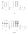
- FIGS. 1 a to 1 k are plan views and cross-sectional views showing a method of manufacturing a semiconductor device including vertical transistors according to an embodiment of the present invention.
- FIGS. 2 a to 2 q are plan views and cross-sectional views showing a method of manufacturing a semiconductor device including vertical transistors according to another embodiment of the present invention.
- FIGS. 1 a to 1 k are plan views and cross-sectional views showing a method of manufacturing a semiconductor device including vertical transistors according to an embodiment of the present invention.
- a vertical transistor is used as a cell transistor included in each of unit cells within a semiconductor memory device is described.
- FIG. 1 a is a plan view showing a cell array region within the semiconductor device
- FIG. 1 b is a cross-sectional view of the semiconductor device taken along line X-X′ in FIG. 1 a.
- a pad oxide layer 104 is formed on a semiconductor substrate 102 .
- a hard mask nitride layer 106 is formed on the pad oxide layer 104 .
- a photoresist layer is coated on the hard mask nitride layer 106 , and a photolithography process using a mask is then performed, thereby forming a first photoresist layer pattern 108 .
- a vertical transistor is used as the cell transistor of a unit cell, a plurality of the vertical transistors is formed so that they are arranged in rows and columns as shown in FIG. 1 a .
- a method of manufacturing the vertical transistors is described below using cross sections taken along X-X′ at different steps of the process.
- the hard mask nitride layer 106 and the pad oxide layer 104 are sequentially etched using the first photoresist layer pattern 108 as an etch mask. The remaining photoresist layer pattern 108 is removed.
- the exposed semiconductor substrate 102 is etched using the partially etched hard mask nitride layer 106 as an etch mask, thereby forming silicon pillars 110 in which channel regions of the vertical transistors will be formed.
- a gate oxide layer 112 is formed on the exposed surface of the semiconductor substrate 102 , including the sides of the silicon pillars 110 .
- a conductive material 114 for a gate electrode is deposited on the entire surface of the structure, including the silicon pillars 110 , and over the semiconductor substrate 102 .
- the conductive material 114 on each side of the silicon pillars is separated from each other.
- Ion implantation for the semiconductor substrate 102 is performed to form bit line regions 116 .
- a nitride layer 118 is formed on the entire surface of the structure.
- a first dielectric interlayer (not shown) is deposited between the silicon pillars 110 .
- a polishing process is carried out until the gate oxide layer 112 is exposed.
- the first dielectric interlayer, the nitride layer 118 , and the conductive material 114 for a gate electrode are removed by performing an etchback process until part of the gate oxide layer 112 formed on the silicon pillars 110 is exposed.
- a channel region, source/drain regions, and a gate electrode 114 A of a transistor is defined within each of the silicon pillars 110 .
- a second dielectric interlayer 120 A is further deposited in such a way as to cover the silicon pillars 110 and the hard mask nitride layer 106 , and a polishing process is then performed.
- a photoresist layer is coated on the polished first dielectric interlayer 120 A.
- a second photoresist layer pattern 122 is formed by performing a photolithography process using a bit line mask.
- the first photoresist layer pattern 108 shown in FIG. 1 b is used to define the positions of the silicon pillars 110 for forming the vertical transistors
- the second photoresist layer pattern 122 shown in FIG. 1 h is used to define the positions of bit lines 116 A and 116 B.
- the exposed first and second dielectric interlayers and 120 A are removed using the second photoresist layer pattern 122 as an etch mask.
- the gate oxide layer 112 exposed between the silicon pillars 110 is etched.
- the bit line region 116 and the semiconductor substrate 102 , exposed between the silicon pillars 110 through the removal of the gate oxide layer 112 are etched, thereby forming bit lines 116 A and 116 B.
- a third dielectric interlayer 124 is deposited between the neighboring bit lines 116 A and 116 B and then polished.
- a photoresist layer (not shown) is coated on the third dielectric interlayer 124 .
- a photolithography process using a mask for defining word lines is carried out, and the photoresist layer is then patterned.
- the third dielectric interlayer 124 exposed by the patterned photoresist layer and the nitride layer 118 formed outside the gate electrode 114 A are etched.
- the third dielectric interlayer 124 is formed in order to electrically fully insulate the neighboring bit lines 116 A and 116 B and also reduce capacitance between the bit lines 116 A and 116 B and word lines. Accordingly, the third dielectric interlayer 124 may preferably remain at a certain height over the bottoms of the neighboring two silicon pillars 110 , rather than being formed solely within trenches of the semiconductor substrate 102 .
- a conductive material is filled in a space formed by the etching of the third dielectric interlayer 124 .
- An etchback process is performed until the gate electrode 114 A is exposed, thereby forming word lines 126 .
- a fourth dielectric interlayer 128 is deposited.
- the hard mask nitride layer 106 and the pad oxide layer 104 are removed by performing a polishing process until the top surfaces of the silicon pillars 110 are exposed.
- the top surface of the silicon pillar 110 exposed by the polishing process become the storage node of the unit cell.
- bit lines As described above, when unit cells including vertical transistors are formed, silicon pillars (i.e., the channel regions of the vertical transistors) are formed and ion implantation is then carried out in order to form bit lines. A doped region is formed at the bottom of the silicon pillars through ion implantation, thereby forming bit line regions. The exposed bit line regions between silicon pillars are removed using a photoresist layer pattern as an etch mask, thereby separating the bit lines from each other.
- a photoresist layer pattern as an etch mask
- bit line region is formed between the neighboring vertical transistors
- part of the bit line region is etched using the photoresist layer pattern as an etch mask to separate the bit line regions.
- an alignment error occurs in the process of forming the photoresist layer pattern used as the etch mask
- a semiconductor device may be defective if the bit line regions are not separated from each other.
- a process margin for forming the photoresist layer pattern for separating the bit line regions is very small. Accordingly, there is a possibility that the production yield may be low because of alignment error.
- the bit lines are formed under the silicon pillars through ion implantation, in the present embodiment, the bit lines are formed of a metal layer in order to lower the resistance of the bit lines.
- the semiconductor substrate is further etched in one of the horizontal and vertical directions, and a metal layer is formed in the etched spaces.
- a metal layer is formed in the etched spaces.
- certain parts of the metal layer can be removed to isolate a row or column of silicon pillars from each other. Accordingly, the plurality of silicon pillars can be connected in either the horizontal direction or the vertical direction through the metal layer.
- bit lines are formed of the metal layer using this method as described above, photoresist layers and masking processes are not required to create the bit lines. Accordingly, the present embodiment can reduce alignment error when photolithography processes are performed several times using masks in which different patterns are defined.
- FIGS. 2 a to 2 q are plan views and cross-sectional views showing a method of manufacturing a semiconductor device including vertical transistors according to another embodiment of the present invention.
- FIG. 2 a is a plan view showing a first photoresist layer pattern 208 formed over a semiconductor substrate 202 and cross-sectional views showing a process of etching the semiconductor substrate 202 using the first photoresist layer pattern 208 as an etch mask.
- the cross sections are taken along line A-A′ and B-B′ in the plan view.
- a pad oxide layer 204 is formed on the semiconductor substrate 202 .
- a first hard mask layer 206 e.g., a nitride layer, is deposited on the pad oxide layer 204 .
- the first photoresist layer pattern 208 is formed on the first hard mask layer 206 .
- the first hard mask layer 206 , the pad oxide layer 204 , and the semiconductor substrate 202 exposed between the first photoresist layer patterns 208 are sequentially etched. With respect to the plan view of FIG. 2 a , the first photoresist layer patterns 208 are formed in a horizontal direction.
- First patterns 210 A having a line form are formed by etching the semiconductor substrate 202 using the first photoresist layer patterns 208 as an etching mask.
- a first spacer layer 252 e.g., an oxide layer, is formed on the sidewalls of the first patterns 210 A and the first hard mask layers 206 .
- an etchback process is carried out so that the first spacer layer 252 remains on the sidewalls of the first patterns 210 A and the first hard mask layers 206 .
- second patterns 210 B are formed by etching the semiconductor substrate 202 to a certain depth using the first spacer oxide layer 252 as an etch mask.
- a metal layer 216 A is formed between the second patterns 210 B. After depositing the metal layer 216 A on the semiconductor substrate 202 and between the second patterns 210 B, an etchback process is carried out so that the first spacer layer 252 is exposed.
- the metal layer 216 A is used as a bit line which connects, in one direction, the lower portions (e.g., transistor drains) of neighboring silicon pillars to be formed later.
- the first spacer layer 252 is removed.
- a first dielectric interlayer 220 is deposited on the metal layer 216 A and is then polished using Chemical Mechanical Polishing (CMP) so that the first hard mask layer 206 is exposed.
- CMP Chemical Mechanical Polishing
- a second hard mask layer 256 is formed on the first hard mask layer 206 and the first dielectric interlayer 220 .
- second photoresist layer patterns 258 are formed in a vertical direction crossing the direction where the first hard mask layer 206 and the first patterns 210 A having a line form are formed.
- subsequent processes are described with reference to the cross section taken along line A-A′, B-B′, C-C′, and D-D′ in the plan view of FIG. 2 e.
- the second hard mask layer 256 is patterned using the second photoresist layer patterns 258 as an etch mask. After the second hard mask layer 256 is patterned, the remaining second photoresist layer patterns 258 are removed.
- silicon pillars 210 C are formed by etching the first dielectric interlayer 220 , the first hard mask layer 206 , the pad oxide layer 204 , and the first patterns 210 A, using the patterned second hard mask layer 256 as an etch mask. The process of etching the first dielectric interlayer 220 and the first patterns 210 A is carried out until a top surface of the metal layer 216 A is exposed.
- a second spacer layer 262 is formed on the sidewalls of the resulting structure, including the silicon pillars 210 C and the first dielectric interlayer 220 .
- the second spacer layer 262 may be formed by depositing an oxide layer and then performing an etchback process in a similar way to the first spacer layer 252 .
- Gutters 266 are formed by isotropically etching the exposed second patterns 210 B using the second spacer layer 262 and the second hard mask layer 256 as an etch mask.
- the exposed second patterns 210 B are isotropically etched, the gutters 266 each having a round concave form is formed at the bottoms of the silicon pillars 210 C.
- the above isotropic etch process differs from the anisotropic etch process used in forming the first and second patterns 210 A and 210 B shown in FIGS. 2 a and 2 b.
- a barrier metal layer 216 B is deposited on the entire surface of the structure, including the silicon pillars 210 C, the first dielectric interlayer 220 , and the second hard mask layer 256 .
- the barrier metal layer 216 B is formed to fill the gutters 266 formed at the bottom of the silicon pillars 210 C.
- the exposed barrier metal layer 216 B (as seen from directly above) and the exposed metal layer 216 A are removed by performing an etchback process.
- the barrier metal layer 216 B and the metal layer 216 A, in contact with silicon, are sintered by performing an annealing process, thereby completing the bit lines. Consequently, the metal layer 216 A connecting the plurality of silicon pillars 210 C remains under the second photoresist layer pattern 258 formed in the vertical direction (as seen from the plan view), but is removed from the remaining regions.
- the regions of the barrier metal layer 216 B, formed to fill the gutters 266 and exposed between the silicon pillars 210 C, are also removed.
- the process of removing the exposed barrier metal layer 216 B and the exposed metal layer 216 A can be carried out with a wet etch process.
- source/drain regions of the vertical transistor, connecting the bit lines formed between the silicon pillars 210 C may be formed under the silicon pillars 210 C. Accordingly, the degree of integration of semiconductor devices can be increased, by allowing the pillars to be spaced closer together. Also, the resistance value of the bit lines can be reduced by using a metal layer rather than forming the bit lines through an ion implantation process. Furthermore, in the present embodiment, since the barrier metal layer 216 B used to fill the gutters 266 of the semiconductor substrate 202 is sintered using an annealing process, the silicon pillars 210 C are less likely to collapse although they have a high aspect ratio.
- the semiconductor substrate 202 exposed between neighboring silicon pillars 210 C is etched to a certain depth using the second hard mask layer 256 and the second spacer layer 262 , formed in the vertical direction where the plurality of silicon pillars 210 C are coupled to each other, as an etch mask. Accordingly, the neighboring bit lines are fully isolated. Next, the remaining second hard mask layer 256 and the remaining second spacer layer 262 are removed.
- a second dielectric interlayer 260 is deposited over the semiconductor substrate 202 .
- a polishing process is then carried out until the surface of the first hard mask layer 206 is exposed.
- the second dielectric interlayer 260 is etched to a certain depth by performing an etchback process using the first hard mask layer 206 as an etch barrier.
- the second dielectric interlayer 260 remains to a certain depth on the metal layer 216 A formed between the silicon pillars 210 C. From the plan view of FIG. 2 l , the positions of the silicon pillars 210 C formed under the first hard mask layer 206 , the positions of the barrier metal layers 216 B formed on the lower sides of the silicon pillars 210 C, and the positions of the metal layers 216 A each connecting the bottoms of the silicon pillars 210 C can be seen.
- a gate oxide layer 212 is formed on the silicon pillars 210 C and the second dielectric interlayer 260 .
- a conductive material is deposited in order to form a gate electrode 214 between the silicon pillars 210 C.
- An etchback process is then carried out so that the gate electrode 214 is formed on the sidewalls of each of the silicon pillars 210 C.
- the gate electrodes 214 are separated from each other so that they are not connected between neighboring silicon pillars 210 C. Consequently, the sidewalls of each of the silicon pillars 210 C is surrounded by the gate oxide layer 212 and the gate electrode 214 .
- a third dielectric interlayer 270 is deposited between the gate electrodes 214 .
- a polishing process is carried out until the top surface of the first hard mask layer 206 is exposed.
- the third dielectric interlayer 270 is removed to a certain depth by performing an etchback process.
- the third dielectric interlayer 270 is removed so that it is lower than the top surface of the silicon pillars 210 C.
- the gate electrodes 214 exposed on the sidewalls of the silicon pillars 210 C are removed, and so the gate electrodes 214 and the third dielectric interlayers 270 are lower in height than the silicon pillars 210 C.
- a photoresist layer is coated on the first hard mask layers 206 and the third dielectric interlayers 270 .
- Third photoresist layer patterns 222 expose regions where word lines will be formed.
- the third photoresist layer patterns 222 are formed to have a line pattern of a horizontal direction similar to the pattern of the first photoresist layer patterns 208 used to form the silicon pillars 210 C. Further, the third photoresist layer patterns 222 also function to prevent the third dielectric interlayer 270 from being removed. Accordingly, the positions of the third photoresist layer patterns 222 differ from those of the first photoresist layer patterns 208 .
- the gate oxide layer 212 exposed between the gate electrodes 214 is removed using the third photoresist layer patterns 222 as an etch mask. Part of the exposed third dielectric interlayer 270 is also removed. Here, for the purpose of electrical insulation between the word lines and the bit lines formed on the lower sides of the silicon pillars 210 C, the third dielectric interlayer 270 partially remains on the gate oxide layer 212 .
- the third photoresist layer patterns 222 remaining after the etching of the third dielectric interlayer 270 are removed.
- a conductive material is deposited on the gate electrodes 214 exposed through the etching of the third dielectric interlayer 270 , and word lines 226 are formed by performing an etchback process.
- a fourth dielectric interlayer 280 is formed on the word lines 226 .
- a polishing process is carried out so that the first hard mask layer 206 over the silicon pillars 210 C is removed, thereby exposing the top surfaces of the silicon pillars 210 C.
- the top surface of each of the silicon pillars 210 C corresponds to a where a storage node (e.g., capacitor for a memory device) would be formed in subsequent processes.
- a unit cell includes a plurality of vertical transistors in each of which conduction regions corresponding to source/drain regions are included on the upper and lower portions of a pillar shape, and the vertical transistors of the unit cells are connected by bit lines including the metal layer having a low resistance value.
- the bit lines of a line form are formed on the lower sides of the silicon pillars. Accordingly, power consumption of a semiconductor memory device can be reduced and operational stability in a low power environment can be guaranteed because the bit lines can be formed of the metal layer, etc. having a low resistance as compared with an implementation where bit lines that are formed through ion implantation.
- the operation of peripheral circuits of a unit cell, such as a sense amp can be facilitated because the amount of current corresponding to data transferred from a cell array within a semiconductor memory device can be increased.
- photoresist layer patterns other than the photoresist layer patterns for forming the silicon pillars are not required. Accordingly, alignment error between micro patterns, easily occurring in a process of forming unit cells within a high-integrated semiconductor memory device, can be reduced greatly. It leads to an improved operating characteristic and increased yield of a semiconductor memory device including the vertical transistors.
- the pattern process of forming the silicon pillars including the channel regions of the vertical transistors is performed twice in opposite directions, and the conductive material is formed in the bit line regions between the twice pattern processes. Accordingly, there is an advantage in that the operating current within a semiconductor device can be increased because the bit lines of the present invention may have a low resistance value as compared with the conventional bit lines formed through ion implantation. Moreover, since the operating current within a semiconductor device can be increased, the operating speed of the semiconductor device can be enhanced or the level of a supply voltage can be lowered, so power consumption of the semiconductor device can be reduced.
- the bit lines are patterned when the pattern process of forming the silicon pillars is performed. Accordingly, alignment error can be prevented because it is not necessary to perform a photolithography process of separating the bit lines between the silicon pillars from each other in the known art, and so the production yield can be improved.
Abstract
Description
Claims (5)
Priority Applications (1)
| Application Number | Priority Date | Filing Date | Title |
|---|---|---|---|
| US13/314,125 US20120077337A1 (en) | 2008-07-31 | 2011-12-07 | Method of manufacturing high-integrated semiconductor device and semiconductor device manufactured using the same |
Applications Claiming Priority (2)
| Application Number | Priority Date | Filing Date | Title |
|---|---|---|---|
| KR1020080075039A KR101037495B1 (en) | 2008-07-31 | 2008-07-31 | Method of fabricating high integrated semiconductor apparatus and semiconductor apparatus fabricated thereby |
| KR10-2008-0075039 | 2008-07-31 |
Related Child Applications (1)
| Application Number | Title | Priority Date | Filing Date |
|---|---|---|---|
| US13/314,125 Division US20120077337A1 (en) | 2008-07-31 | 2011-12-07 | Method of manufacturing high-integrated semiconductor device and semiconductor device manufactured using the same |
Publications (2)
| Publication Number | Publication Date |
|---|---|
| US20100025758A1 US20100025758A1 (en) | 2010-02-04 |
| US8119509B2 true US8119509B2 (en) | 2012-02-21 |
Family
ID=41607440
Family Applications (2)
| Application Number | Title | Priority Date | Filing Date |
|---|---|---|---|
| US12/495,554 Expired - Fee Related US8119509B2 (en) | 2008-07-31 | 2009-06-30 | Method of manufacturing high-integrated semiconductor device and semiconductor device manufactured using the same |
| US13/314,125 Abandoned US20120077337A1 (en) | 2008-07-31 | 2011-12-07 | Method of manufacturing high-integrated semiconductor device and semiconductor device manufactured using the same |
Family Applications After (1)
| Application Number | Title | Priority Date | Filing Date |
|---|---|---|---|
| US13/314,125 Abandoned US20120077337A1 (en) | 2008-07-31 | 2011-12-07 | Method of manufacturing high-integrated semiconductor device and semiconductor device manufactured using the same |
Country Status (4)
| Country | Link |
|---|---|
| US (2) | US8119509B2 (en) |
| KR (1) | KR101037495B1 (en) |
| CN (1) | CN101640201B (en) |
| TW (1) | TWI512948B (en) |
Cited By (1)
| Publication number | Priority date | Publication date | Assignee | Title |
|---|---|---|---|---|
| US20120270395A1 (en) * | 2011-04-25 | 2012-10-25 | Ku Mi-Na | Method for fabricating metal pattern in semiconductor device |
Families Citing this family (7)
| Publication number | Priority date | Publication date | Assignee | Title |
|---|---|---|---|---|
| KR100900148B1 (en) * | 2007-10-31 | 2009-06-01 | 주식회사 하이닉스반도체 | Semicoductor device and method of fabricating the same |
| JP2009141073A (en) * | 2007-12-05 | 2009-06-25 | Elpida Memory Inc | Method of manufacturing semiconductor device, and semiconductor device |
| KR101087877B1 (en) * | 2008-12-23 | 2011-11-30 | 주식회사 하이닉스반도체 | Method of fabricating high integrated semiconductor apparatus and semiconductor apparatus fabricated thereby |
| KR101093627B1 (en) | 2010-09-28 | 2011-12-15 | 주식회사 하이닉스반도체 | Method for fabricating semiconductor device |
| US8735280B1 (en) | 2012-12-21 | 2014-05-27 | Taiwan Semiconductor Manufacturing Company, Ltd. | Method of semiconductor integrated circuit fabrication |
| DE102016107203B4 (en) * | 2016-04-19 | 2021-12-23 | Infineon Technologies Austria Ag | Power semiconductor device trench with field plate and gate electrode and method for production |
| CN113644065B (en) * | 2020-04-27 | 2024-03-29 | 长鑫存储技术有限公司 | Semiconductor structure and forming method thereof, memory and forming method thereof |
Citations (5)
| Publication number | Priority date | Publication date | Assignee | Title |
|---|---|---|---|---|
| US20060043450A1 (en) | 2004-09-02 | 2006-03-02 | Tang Sanh D | Vertical transistors |
| KR20070009140A (en) | 2005-07-15 | 2007-01-18 | 삼성전자주식회사 | Semiconductor device with vertical channel improved contact resistance and method of manufacturing the same |
| KR20070038233A (en) | 2005-10-05 | 2007-04-10 | 삼성전자주식회사 | Circuitry device comprising vertical transistors with buried bit lines and manufacturing method for the same |
| KR100723527B1 (en) | 2006-02-13 | 2007-05-30 | 삼성전자주식회사 | Method of manufacturing semiconductor device including vertical channel transistor and semiconductor device fabricated using the same |
| US7531412B2 (en) | 2004-11-08 | 2009-05-12 | Samsung Electronics Co., Ltd. | Methods of manufacturing semiconductor memory devices including a vertical channel transistor |
Family Cites Families (3)
| Publication number | Priority date | Publication date | Assignee | Title |
|---|---|---|---|---|
| DE59814170D1 (en) * | 1997-12-17 | 2008-04-03 | Qimonda Ag | Memory cell arrangement and method for its production |
| US7235471B2 (en) * | 2004-05-26 | 2007-06-26 | Freescale Semiconductor, Inc. | Method for forming a semiconductor device having a silicide layer |
| KR100725370B1 (en) * | 2006-01-05 | 2007-06-07 | 삼성전자주식회사 | Method for fabricating a semiconductor device and semiconductor device by the same |
-
2008
- 2008-07-31 KR KR1020080075039A patent/KR101037495B1/en active IP Right Grant
-
2009
- 2009-06-30 US US12/495,554 patent/US8119509B2/en not_active Expired - Fee Related
- 2009-07-16 TW TW098124064A patent/TWI512948B/en not_active IP Right Cessation
- 2009-07-21 CN CN2009101576173A patent/CN101640201B/en not_active Expired - Fee Related
-
2011
- 2011-12-07 US US13/314,125 patent/US20120077337A1/en not_active Abandoned
Patent Citations (5)
| Publication number | Priority date | Publication date | Assignee | Title |
|---|---|---|---|---|
| US20060043450A1 (en) | 2004-09-02 | 2006-03-02 | Tang Sanh D | Vertical transistors |
| US7531412B2 (en) | 2004-11-08 | 2009-05-12 | Samsung Electronics Co., Ltd. | Methods of manufacturing semiconductor memory devices including a vertical channel transistor |
| KR20070009140A (en) | 2005-07-15 | 2007-01-18 | 삼성전자주식회사 | Semiconductor device with vertical channel improved contact resistance and method of manufacturing the same |
| KR20070038233A (en) | 2005-10-05 | 2007-04-10 | 삼성전자주식회사 | Circuitry device comprising vertical transistors with buried bit lines and manufacturing method for the same |
| KR100723527B1 (en) | 2006-02-13 | 2007-05-30 | 삼성전자주식회사 | Method of manufacturing semiconductor device including vertical channel transistor and semiconductor device fabricated using the same |
Cited By (2)
| Publication number | Priority date | Publication date | Assignee | Title |
|---|---|---|---|---|
| US20120270395A1 (en) * | 2011-04-25 | 2012-10-25 | Ku Mi-Na | Method for fabricating metal pattern in semiconductor device |
| US8513132B2 (en) * | 2011-04-25 | 2013-08-20 | Hynix Semiconductor Inc. | Method for fabricating metal pattern in semiconductor device |
Also Published As
| Publication number | Publication date |
|---|---|
| US20120077337A1 (en) | 2012-03-29 |
| TW201007928A (en) | 2010-02-16 |
| KR101037495B1 (en) | 2011-05-26 |
| CN101640201B (en) | 2013-02-27 |
| TWI512948B (en) | 2015-12-11 |
| US20100025758A1 (en) | 2010-02-04 |
| CN101640201A (en) | 2010-02-03 |
| KR20100013499A (en) | 2010-02-10 |
Similar Documents
| Publication | Publication Date | Title |
|---|---|---|
| US8119509B2 (en) | Method of manufacturing high-integrated semiconductor device and semiconductor device manufactured using the same | |
| US8344517B2 (en) | Integrated circuit devices including air spacers separating conductive structures and contact plugs and methods of fabricating the same | |
| US9236501B2 (en) | Dummy bit line MOS capacitor and device using the same | |
| KR100461929B1 (en) | Semiconductor memory device and method for manufacturing the same | |
| US8507980B2 (en) | Semiconductor devices having bit line interconnections with increased width and reduced distance from corresponding bit line contacts and methods of fabricating such devices | |
| US20140264549A1 (en) | Vertical memory devices with vertical isolation structures and methods of fabricating the same | |
| US7691689B2 (en) | Methods of fabricating semiconductor devices having multiple channel transistors and semiconductor devices fabricated thereby | |
| US8871591B2 (en) | Methods of manufacturing a vertical type semiconductor device | |
| US8415738B2 (en) | Semiconductor memory device and manufacturing method thereof | |
| JP2011018825A (en) | Semiconductor device and method of manufacturing the same | |
| US8026547B2 (en) | Semiconductor memory device and method of manufacturing the same | |
| KR20100098134A (en) | Method of fabricating semiconductor device having capacitor under bitline structure | |
| KR100475075B1 (en) | Semiconductor memory device and method for manufacturing the same | |
| US6930000B2 (en) | Method of manufacturing semiconductor device | |
| JP2005174977A (en) | Ferroelectric storage device and manufacturing method therefor | |
| CN101859777A (en) | Structure and fabricating process of non-volatile memory | |
| US7312489B2 (en) | Memory cell having bar-shaped storage node contact plugs and methods of fabricating same | |
| CN100464422C (en) | Hollow cylindrical capacitor and its producing method | |
| KR20210014828A (en) | Semiconductor memory and method for forming the same | |
| US20110159682A1 (en) | Methods of manufacturing memory devices | |
| US20150255465A1 (en) | Semiconductor device, and manufacturing method for same | |
| KR20110013701A (en) | Semiconductor device and method for fabricating the same | |
| KR101140010B1 (en) | Semiconductor device and method for forming the same | |
| CN101241898A (en) | Semiconductor device and manufacturing method thereof | |
| CN117037874A (en) | Semiconductor device and method for forming the same |
Legal Events
| Date | Code | Title | Description |
|---|---|---|---|
| AS | Assignment |
Owner name: HYNIX SEMICONDUCTOR INC,KOREA, REPUBLIC OF Free format text: ASSIGNMENT OF ASSIGNORS INTEREST;ASSIGNOR:CHO, YOUNG MAN;REEL/FRAME:022933/0992 Effective date: 20090626 Owner name: HYNIX SEMICONDUCTOR INC, KOREA, REPUBLIC OF Free format text: ASSIGNMENT OF ASSIGNORS INTEREST;ASSIGNOR:CHO, YOUNG MAN;REEL/FRAME:022933/0992 Effective date: 20090626 |
|
| ZAAA | Notice of allowance and fees due |
Free format text: ORIGINAL CODE: NOA |
|
| ZAAB | Notice of allowance mailed |
Free format text: ORIGINAL CODE: MN/=. |
|
| FEPP | Fee payment procedure |
Free format text: PAYOR NUMBER ASSIGNED (ORIGINAL EVENT CODE: ASPN); ENTITY STATUS OF PATENT OWNER: LARGE ENTITY |
|
| STCF | Information on status: patent grant |
Free format text: PATENTED CASE |
|
| FPAY | Fee payment |
Year of fee payment: 4 |
|
| MAFP | Maintenance fee payment |
Free format text: PAYMENT OF MAINTENANCE FEE, 8TH YEAR, LARGE ENTITY (ORIGINAL EVENT CODE: M1552); ENTITY STATUS OF PATENT OWNER: LARGE ENTITY Year of fee payment: 8 |
|
| FEPP | Fee payment procedure |
Free format text: MAINTENANCE FEE REMINDER MAILED (ORIGINAL EVENT CODE: REM.); ENTITY STATUS OF PATENT OWNER: LARGE ENTITY |
|
| LAPS | Lapse for failure to pay maintenance fees |
Free format text: PATENT EXPIRED FOR FAILURE TO PAY MAINTENANCE FEES (ORIGINAL EVENT CODE: EXP.); ENTITY STATUS OF PATENT OWNER: LARGE ENTITY |
|
| STCH | Information on status: patent discontinuation |
Free format text: PATENT EXPIRED DUE TO NONPAYMENT OF MAINTENANCE FEES UNDER 37 CFR 1.362 |
|
| FP | Lapsed due to failure to pay maintenance fee |
Effective date: 20240221 |