US8184899B2 - Method of detecting a defect on an object - Google Patents
Method of detecting a defect on an object Download PDFInfo
- Publication number
- US8184899B2 US8184899B2 US12/383,017 US38301709A US8184899B2 US 8184899 B2 US8184899 B2 US 8184899B2 US 38301709 A US38301709 A US 38301709A US 8184899 B2 US8184899 B2 US 8184899B2
- Authority
- US
- United States
- Prior art keywords
- reference image
- gray level
- pixels
- defect
- preliminary
- Prior art date
- Legal status (The legal status is an assumption and is not a legal conclusion. Google has not performed a legal analysis and makes no representation as to the accuracy of the status listed.)
- Active, expires
Links
- 230000007547 defect Effects 0.000 title claims abstract description 61
- 238000000034 method Methods 0.000 title claims abstract description 55
- 238000007689 inspection Methods 0.000 claims abstract description 39
- 239000004065 semiconductor Substances 0.000 claims description 36
- 239000000758 substrate Substances 0.000 claims description 24
- 238000001514 detection method Methods 0.000 description 4
- 230000002093 peripheral effect Effects 0.000 description 4
- 230000010339 dilation Effects 0.000 description 3
- 238000009499 grossing Methods 0.000 description 3
- 238000002513 implantation Methods 0.000 description 3
- 238000004519 manufacturing process Methods 0.000 description 2
- 230000002159 abnormal effect Effects 0.000 description 1
- 230000002411 adverse Effects 0.000 description 1
- 238000004140 cleaning Methods 0.000 description 1
- 238000007796 conventional method Methods 0.000 description 1
- 238000005137 deposition process Methods 0.000 description 1
- 239000007943 implant Substances 0.000 description 1
- 238000000059 patterning Methods 0.000 description 1
- 238000005498 polishing Methods 0.000 description 1
- 239000000126 substance Substances 0.000 description 1
Images


Classifications
-
- H—ELECTRICITY
- H01—ELECTRIC ELEMENTS
- H01L—SEMICONDUCTOR DEVICES NOT COVERED BY CLASS H10
- H01L22/00—Testing or measuring during manufacture or treatment; Reliability measurements, i.e. testing of parts without further processing to modify the parts as such; Structural arrangements therefor
-
- G—PHYSICS
- G06—COMPUTING; CALCULATING OR COUNTING
- G06T—IMAGE DATA PROCESSING OR GENERATION, IN GENERAL
- G06T7/00—Image analysis
- G06T7/0002—Inspection of images, e.g. flaw detection
- G06T7/0004—Industrial image inspection
-
- G—PHYSICS
- G06—COMPUTING; CALCULATING OR COUNTING
- G06T—IMAGE DATA PROCESSING OR GENERATION, IN GENERAL
- G06T2207/00—Indexing scheme for image analysis or image enhancement
- G06T2207/30—Subject of image; Context of image processing
- G06T2207/30108—Industrial image inspection
- G06T2207/30148—Semiconductor; IC; Wafer
Definitions
- Example embodiments relate to a method of detecting a defect on an object. More particularly, example embodiments relate to a method of detecting a defect generated, or otherwise present, on a semiconductor substrate.
- semiconductor devices are manufactured by various processes including a deposition process, a patterning process, a chemical mechanical polishing (CMP) process, a cleaning process, and other processes.
- CMP chemical mechanical polishing
- Each process can introduce various types of defects on the semiconductor substrate, which can adversely affect the resulting semiconductor device. Therefore, a detection process for detecting the defects is performed so that decisions can be made for rectifying the defects, thereby improving device yield and reliability.
- a semiconductor substrate can be divided into a plurality of inspection regions.
- An inspection image of an inspected region can be compared with a reference image of a nearby inspection region to identify defects in the inspected region.
- the presence of defects in the inspected region is determined using only a single reference image.
- a cell region and a peripheral region In contemporary memory devices it is common for both a cell region and a peripheral region to be present in each of the dies on the semiconductor substrate.
- the cell region and the peripheral region can quite commonly have different reflective properties and scattering coefficients with respect to the incident inspection light. Further, certain differences in properties such as layer thickness can exist between dies located at a central portion and an edge portion of the semiconductor substrate. That is, certain regions of the semiconductor substrate can have clearly discriminated brightness properties.
- the conventional inspection method may vary in effectiveness with respect to position of the inspected region on the semiconductor substrate or with respect to the brightness of the inspected region.
- Example embodiments provide a method of accurately detecting a defect on an object that may have substantially the same detectability with respect to inspection regions having different brightnesses.
- a method of detecting a defect on an object In the method of detecting the defect on the object, a preliminary reference image is obtained from a plurality of comparison regions defined on the object. The preliminary reference image is divided into reference zones by a similar brightness. Each of the reference zones is provided with substantially the same gray level, respectively, to obtain a reference image. Whether a defect exists in an inspection region among the comparison regions is determined using the reference image.
- obtaining the preliminary reference image includes obtaining a gray level average of pixels located on substantially the same coordinate in each of the comparison regions.
- obtaining the reference image includes providing all of the pixels in the reference zone with a maximum vale of gray level averages of the pixels in the reference zone.
- obtaining the reference image includes providing all of the pixels in the reference zone with a mean of the gray level averages of the pixels in the reference zone.
- determining whether the defect exists in the inspection region includes calculating a plurality of standard deviations with respect to gray levels of the reference image, and determining whether the defect exists in the inspection region uses gray levels of the inspection region and the standard deviations.
- a method of detecting a defect on a semiconductor substrate In the method of detecting the defect on the semiconductor substrate, a gray level average of pixels located at substantially a same coordinate in each of cells of a die in the semiconductor substrate is calculated to obtain a preliminary reference image.
- the preliminary reference image is divided into reference zones by a similar brightness. Each of the reference zones is provided with substantially the same gray level, respectively, to obtain a reference image.
- a plurality of standard deviations with respect to gray levels of the reference image is calculated. Whether a defect exists in the cell is determined using the standard deviations and the gray levels of the cell.
- obtaining the reference image can include providing all of the pixels in the reference zone with a maximum vale of gray level averages of the pixels in the reference zone.
- obtaining the reference image can include providing all of the pixels in the reference zone with a mean of the gray level averages of the pixels in the reference zone.
- a method of detecting a defect on a semiconductor substrate In the method of detecting the defect on the semiconductor substrate, a gray level average of pixels located at substantially a same coordinate in each of dies in the semiconductor substrate is calculated to obtain a preliminary reference image.
- the preliminary reference image is divided into reference zones by a similar brightness. Each of the reference zones is provided with substantially the same gray level, respectively, to obtain a reference image.
- a plurality of standard deviations with respect to gray levels of the reference image is calculated. Whether a defect exists in the die is determined using the standard deviations and the gray levels of the die.
- the reference zones include a central portion, a middle portion and an edge portion of the semiconductor substrate.
- obtaining the reference image can include providing all of the dies in the reference zone with a maximum vale of gray level averages of the dies in the reference zone.
- obtaining the reference image can include providing all of the dies in the reference zone with a mean of the gray level averages of the dies in the reference zone.
- defects present in the inspection regions having different brightnesses may be detected using the properly obtained reference image.
- defect detectability with respect to the inspection regions is stabilized.
- defects present on the semiconductor substrate can be accurately detected.
- FIGS. 1 to 5 represent non-limiting, example embodiments as described herein.
- FIG. 1 is a flow chart illustrating a method of detecting a defect on an object in accordance with a first example embodiment of the present invention
- FIG. 2 is a scanning electron microscope (SEM) picture showing a preliminary reference image.
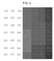
- FIG. 3 is a SEM picture illustrating a reference image
- FIG. 4 is a graph illustrating pixel numbers with respect to gray levels of the reference image in FIG. 3 ;
- FIG. 5 is a flow chart illustrating a method of detecting a defect on an object in accordance with a second example embodiment of the present invention.
- first, second, third etc. may be used herein to describe various elements, components, regions, layers and/or sections, these elements, components, regions, layers and/or sections should not be limited by these terms. These terms are only used to distinguish one element, component, region, layer or section from another region, layer or section. Thus, a first element, component, region, layer or section discussed below could be termed a second element, component, region, layer or section without departing from the teachings of the present invention.
- spatially relative terms such as “beneath,” “below,” “lower,” “above,” “upper” and the like, may be used herein for ease of description to describe one element or feature's relationship to another element(s) or feature(s) as illustrated in the figures. It will be understood that the spatially relative terms are intended to encompass different orientations of the device in use or operation in addition to the orientation depicted in the figures. For example, if the device in the figures is turned over, elements described as “below” or “beneath” other elements or features would then be oriented “above” the other elements or features. Thus, the exemplary term “below” can encompass both an orientation of above and below. The device may be otherwise oriented (rotated 90 degrees or at other orientations) and the spatially relative descriptors used herein interpreted accordingly.
- Example embodiments are described herein with reference to cross-sectional illustrations that are schematic illustrations of idealized example embodiments (and intermediate structures). As such, variations from the shapes of the illustrations as a result, for example, of manufacturing techniques and/or tolerances, are to be expected. Thus, example embodiments should not be construed as limited to the particular shapes of regions illustrated herein but are to include deviations in shapes that result, for example, from manufacturing. For example, an implanted region illustrated as a rectangle will, typically, have rounded or curved features and/or a gradient of implant concentration at its edges rather than a binary change from implanted to non-implanted region.
- a buried region formed by implantation may result in some implantation in the region between the buried region and the surface through which the implantation takes place.
- the regions illustrated in the figures are schematic in nature and their shapes are not intended to illustrate the actual shape of a region of a device and are not intended to limit the scope of the present invention.
- FIG. 1 is a flow chart illustrating a method of detecting a defect on an object in accordance with a first example embodiment of the present invention.
- the object to which the method of detecting the defect may be applied can include a semiconductor die having a plurality of cells formed thereon. Further, the semiconductor die may include a cell region and a peripheral region configured to surround or encompass the cell region. Patterns can be repeatedly and regularly arranged in the cell region, while patterns can be irregularly arranged in the peripheral region.
- the semiconductor die in step ST 100 , can be divided into a plurality of comparison regions.
- the comparison regions can correspond to the cell region.
- step ST 102 actual images of the comparison regions can be obtained.
- the actual images can be obtained by using light reflected from the comparison regions or by scanning the comparison regions.
- step ST 104 gray levels of pixels in the actual images are measured.
- the gray levels can be measured simultaneously with the operation of obtaining of the actual images.
- a preliminary reference image is obtained from the actual images.
- gray level averages of each of the actual pixels, which may be located proximal to substantially the same coordinate on the die, in the actual images can be calculated.
- Preliminary reference pixels can be provided with the gray level averages, respectively, to obtain the preliminary reference image. That is, the preliminary reference pixels in the preliminary reference image may have the gray level average of the actual image by the pixel.
- the preliminary reference image is divided into reference zones according to similar brightness levels or values.
- the reference zones may be defined by determining boundary lines between those preliminary reference pixels having sharply different gray levels.
- FIG. 2 is a scanning electron microscope (SEM) picture showing an example preliminary reference image. As shown in FIG. 2 , the preliminary reference pixels having similar brightness values may be located in each of the reference zones.
- step ST 110 all of the preliminary reference pixels in the reference zone may be provided with substantially the same gray level to obtain a reference image. That is, the reference pixels in a reference zone of the reference image may have substantially the same gray level.
- the preliminary reference pixels can be provided with the substantially the same gray level according to their reference zones to remove noise caused by an error in obtaining the preliminary reference image.
- the excessively low gray level may be determined to be caused by the error in measuring the preliminary reference image.
- the excessively low gray level may be removed from the reference image in order to obtain a more accurate reference image.
- the removal of noise can be performed, for example, by the following two processes.
- the noise may be removed by a dilation technique.
- a dilation technique a maximum value of the gray levels of the preliminary reference pixels in the reference zone is determined. All of the gray levels of the preliminary reference pixels are then converted to the maximum value.
- FIG. 3 is a SEM picture illustrating the reference image. As shown in FIG. 3 , all of the reference pixels in the reference zone are given substantially the same maximum value.
- the noise may be removed by a smoothing technique.
- the gray level average of the preliminary reference pixels in the reference zone is calculated.
- the gray levels of the preliminary reference pixels are then converted to the gray level average.
- a graph showing reference pixel numbers with respect to the gray levels of the reference image can be drawn.
- the horizontal axis of the graph represents the gray level and a vertical axis represents the number of reference pixels having a certain gray level.
- a standard deviation of the reference pixel with respect to the gray level can be calculated based on a graph such as the graph of FIG. 4 .
- the reference image can be partitioned according to relative brightnesses, at least two standard deviation values can be obtained for the reference pixel.
- step ST 116 whether a defect may exist or not in an inspection region of the comparison regions can be determined based on the standard deviations and the actual gray levels of the actual image.
- the existence of the defect in the inspection region can be determined based on whether a difference between the actual gray level of the inspection region and the gray level average and a difference between the reference gray level of the reference image and the gray level average is or is not within the standard deviations.
- any one of the reference zones including an inspection position in the comparison regions can be identified.
- the standard deviation corresponding to the identified reference zone may be set as a standard for determining the existence of the defect in the inspection region. That is, the different standard deviations can be applied to the reference zones, respectively. Therefore, the inspection regions will have substantially the same defect detectability, even though they may have different brightness levels.
- the reference image can be divided into reference zones by the different brightnesses.
- defect detectability with respect to the inspection region can be stabilized, irrespective of brightness.
- a defect present on the semiconductor die can be accurately detected.
- FIG. 5 is a flow chart illustrating a method of detecting a defect on an object in accordance with a second example embodiment of the present invention.
- the object to which the method of detecting the defect may be applied may include a semiconductor substrate where a plurality of dies may be formed. Further, the dies in a central portion, the dies in an edge portion and the dies in a middle portion of the semiconductor substrate may have different brightnesses.
- the semiconductor substrate may be divided into a plurality of comparison regions.
- step ST 202 actual images of the comparison regions can be obtained.
- step ST 204 gray levels of the dies in the actual images can be measured.
- a preliminary reference image is obtained from the actual images.
- gray level averages of each of the actual dies which may be located proximal to substantially the same coordinate on the die, in the actual images can be calculated.
- Preliminary reference dies can be provided with the gray level averages, respectively, to obtain the preliminary reference image. That is, the preliminary reference dies in the preliminary reference image may have the gray level average of the actual image by the dies.
- the preliminary reference image is divided into reference zones by according to similar brightness levels or values.
- the reference zones may be defined by determining boundary lines between those preliminary reference dies having sharply different gray levels.
- the reference zones may include the central portion, the middle portion, and the edge portion of the semiconductor substrate. Further, the reference zones may be determined manually by an inspector or automatically by an inspection tool.
- step ST 210 all of the preliminary reference dies in the reference zone may be provided with substantially the same gray level to obtain a reference image. That is, the reference dies in a reference zone of the reference image may have substantially the same gray level. Removal of noise, can, for example, be performed by the dilation technique or the smoothing technique described above in connection with the first embodiment.
- step ST 212 a graph showing reference die numbers with respect to the gray levels of the reference image can be drawn.
- a standard deviation of the reference die with respect to the gray level can be calculated based on a graph determined at step ST 212 .
- the reference image can be partitioned according to relative brightness, at least two standard deviation values can be obtained for the reference die.
- step ST 216 whether a defect may exist or not in an inspection region of the comparison regions can be determined based on the standard deviations and the actual gray levels of the actual image.
- the existence of the defect in the inspection region can be determined based on whether a difference between the actual gray level of the inspection region and the gray level average and a difference between the reference gray level of the reference image and the gray level average is or is not within the standard deviations.
- any one of the reference zones including an inspection position in the inspection region can be identified.
- the standard deviation corresponding to the identified reference zone may be set as a standard for determining the existence of the defect in the inspection region. That is, the different standard deviations can be applied to the reference zones, respectively. Therefore, the inspection regions will have substantially the same defect detectability, even though they may have different brightness levels.
- the reference image can be divided into reference zones by the different brightnesses.
- defect detectability with respect to the inspection region can be stabilized, irrespective of brightness.
- a defect present on the semiconductor die can be accurately detected.
- defects present in inspection regions having different brightnesses may be detected using the properly obtained reference image.
- defect detectability with respect to the inspection regions can be stabilized.
- defects present on the semiconductor substrate can be accurately detected.
Abstract
Description
Claims (15)
Applications Claiming Priority (3)
| Application Number | Priority Date | Filing Date | Title |
|---|---|---|---|
| KR1020080025901 | 2008-03-20 | ||
| KR1020080025901A KR20090100615A (en) | 2008-03-20 | 2008-03-20 | Method of detecting a defect on an object |
| KR10-2008-0025901 | 2008-03-20 |
Publications (2)
| Publication Number | Publication Date |
|---|---|
| US20090238445A1 US20090238445A1 (en) | 2009-09-24 |
| US8184899B2 true US8184899B2 (en) | 2012-05-22 |
Family
ID=41088988
Family Applications (1)
| Application Number | Title | Priority Date | Filing Date |
|---|---|---|---|
| US12/383,017 Active 2030-10-09 US8184899B2 (en) | 2008-03-20 | 2009-03-19 | Method of detecting a defect on an object |
Country Status (2)
| Country | Link |
|---|---|
| US (1) | US8184899B2 (en) |
| KR (1) | KR20090100615A (en) |
Cited By (1)
| Publication number | Priority date | Publication date | Assignee | Title |
|---|---|---|---|---|
| US20190130552A1 (en) * | 2017-10-30 | 2019-05-02 | Samsung Electronics Co., Ltd. | Methods of inspecting defect and methods of fabricating a semiconductor device using the same |
Families Citing this family (9)
| Publication number | Priority date | Publication date | Assignee | Title |
|---|---|---|---|---|
| US9916653B2 (en) * | 2012-06-27 | 2018-03-13 | Kla-Tenor Corporation | Detection of defects embedded in noise for inspection in semiconductor manufacturing |
| KR102583036B1 (en) * | 2015-10-26 | 2023-09-27 | 세메스 주식회사 | Method of inspecting a substrate |
| KR102446956B1 (en) * | 2016-05-12 | 2022-09-23 | 세메스 주식회사 | Method of detecting image noise of camera |
| CN105931976B (en) * | 2016-05-25 | 2019-01-04 | 上海华力微电子有限公司 | A kind of bright field scanning device defines the detection method of scanning area automatically |
| JP6546125B2 (en) * | 2016-06-28 | 2019-07-17 | 学校法人梅村学園 | Defect inspection device |
| CN107833841A (en) * | 2017-10-27 | 2018-03-23 | 德淮半导体有限公司 | Defect inspection method |
| CN111667448B (en) * | 2019-03-06 | 2023-08-15 | 深圳中科飞测科技股份有限公司 | Image processing method, device and equipment |
| CN111724335A (en) | 2019-03-21 | 2020-09-29 | 深圳中科飞测科技有限公司 | Detection method and detection system |
| TWI737375B (en) * | 2020-07-01 | 2021-08-21 | 力晶積成電子製造股份有限公司 | Defect identification method and image analysis system |
Citations (10)
| Publication number | Priority date | Publication date | Assignee | Title |
|---|---|---|---|---|
| JPH07190739A (en) | 1993-12-27 | 1995-07-28 | Sharp Corp | Appearance inspection method for semi-conductor chip and its device |
| JP2002054915A (en) | 2000-08-08 | 2002-02-20 | Sony Corp | Inspection device |
| JP2003270168A (en) | 2002-03-20 | 2003-09-25 | Seiko Epson Corp | Defect inspection method and method for manufacturing semiconductor device |
| KR100425447B1 (en) | 2001-05-10 | 2004-03-30 | 삼성전자주식회사 | Method of grey level compensation and selective wafer-defect inspection for patterns and recording medium recorded thereof |
| KR100474571B1 (en) | 2002-09-23 | 2005-03-10 | 삼성전자주식회사 | Method of setting reference images, method and apparatus using the setting method for inspecting patterns on a wafer |
| KR20060077660A (en) | 2004-12-30 | 2006-07-05 | 동부일렉트로닉스 주식회사 | Method for wafer inspection with auto segment define |
| US20070165939A1 (en) * | 2000-09-10 | 2007-07-19 | Orbotech Ltd | Reduction of false alarms in pcb inspection |
| US7660687B1 (en) * | 2006-05-25 | 2010-02-09 | Kla-Tencor Corporation | Robust measurement of parameters |
| US7804993B2 (en) * | 2005-02-28 | 2010-09-28 | Applied Materials South East Asia Pte. Ltd. | Method and apparatus for detecting defects in wafers including alignment of the wafer images so as to induce the same smear in all images |
| US7925072B2 (en) * | 2007-03-08 | 2011-04-12 | Kla-Tencor Technologies Corp. | Methods for identifying array areas in dies formed on a wafer and methods for setting up such methods |
-
2008
- 2008-03-20 KR KR1020080025901A patent/KR20090100615A/en active IP Right Grant
-
2009
- 2009-03-19 US US12/383,017 patent/US8184899B2/en active Active
Patent Citations (10)
| Publication number | Priority date | Publication date | Assignee | Title |
|---|---|---|---|---|
| JPH07190739A (en) | 1993-12-27 | 1995-07-28 | Sharp Corp | Appearance inspection method for semi-conductor chip and its device |
| JP2002054915A (en) | 2000-08-08 | 2002-02-20 | Sony Corp | Inspection device |
| US20070165939A1 (en) * | 2000-09-10 | 2007-07-19 | Orbotech Ltd | Reduction of false alarms in pcb inspection |
| KR100425447B1 (en) | 2001-05-10 | 2004-03-30 | 삼성전자주식회사 | Method of grey level compensation and selective wafer-defect inspection for patterns and recording medium recorded thereof |
| JP2003270168A (en) | 2002-03-20 | 2003-09-25 | Seiko Epson Corp | Defect inspection method and method for manufacturing semiconductor device |
| KR100474571B1 (en) | 2002-09-23 | 2005-03-10 | 삼성전자주식회사 | Method of setting reference images, method and apparatus using the setting method for inspecting patterns on a wafer |
| KR20060077660A (en) | 2004-12-30 | 2006-07-05 | 동부일렉트로닉스 주식회사 | Method for wafer inspection with auto segment define |
| US7804993B2 (en) * | 2005-02-28 | 2010-09-28 | Applied Materials South East Asia Pte. Ltd. | Method and apparatus for detecting defects in wafers including alignment of the wafer images so as to induce the same smear in all images |
| US7660687B1 (en) * | 2006-05-25 | 2010-02-09 | Kla-Tencor Corporation | Robust measurement of parameters |
| US7925072B2 (en) * | 2007-03-08 | 2011-04-12 | Kla-Tencor Technologies Corp. | Methods for identifying array areas in dies formed on a wafer and methods for setting up such methods |
Cited By (1)
| Publication number | Priority date | Publication date | Assignee | Title |
|---|---|---|---|---|
| US20190130552A1 (en) * | 2017-10-30 | 2019-05-02 | Samsung Electronics Co., Ltd. | Methods of inspecting defect and methods of fabricating a semiconductor device using the same |
Also Published As
| Publication number | Publication date |
|---|---|
| US20090238445A1 (en) | 2009-09-24 |
| KR20090100615A (en) | 2009-09-24 |
Similar Documents
| Publication | Publication Date | Title |
|---|---|---|
| US8184899B2 (en) | Method of detecting a defect on an object | |
| US7200258B2 (en) | Method for selecting reference images, method and apparatus for inspecting patterns on wafers, and method for dividing a wafer into application regions | |
| US7747063B2 (en) | Method and apparatus for inspecting a substrate | |
| JP5641463B2 (en) | Defect inspection apparatus and method | |
| US20120155740A1 (en) | Method of detecting defect in pattern and apparatus for performing the same | |
| US7925072B2 (en) | Methods for identifying array areas in dies formed on a wafer and methods for setting up such methods | |
| US20050179910A1 (en) | System and method for measuring thin film thickness variations and for compensating for the variations | |
| JP2010534408A5 (en) | ||
| JP2003215060A (en) | Pattern inspection method and inspection apparatus | |
| CN103346104A (en) | Method for detecting chip defects | |
| JP2012049503A (en) | Inspection device for semiconductor device, and inspection method for semiconductor device | |
| US20040141640A1 (en) | Method for apparatus for detecting defects on a wafer | |
| US8055057B2 (en) | Method for detecting defects in a substrate having a semiconductor device thereon | |
| US7466853B2 (en) | Method and apparatus for detecting defects on a wafer | |
| WO2012132273A1 (en) | Exterior inspection method and device for same | |
| US20080205746A1 (en) | Method of inspecting an identification mark, method of inspecting a wafer using the same, and apparatus for performing the method | |
| KR101702752B1 (en) | Method of inspecting electronic components | |
| US20230132264A1 (en) | Method of testing display device | |
| KR100774826B1 (en) | Method for detecting the defect of wafer | |
| CN114972147A (en) | Method and device for detecting wafer defects | |
| CN111862076B (en) | Method for improving bright field defect detection precision and noise caused by chromatic aberration in process of bright field defect detection precision | |
| US7382450B2 (en) | Method of detecting an edge bead removal line on a wafer | |
| US20070025609A1 (en) | Method of detecting defect of a pattern in a semiconductor device | |
| KR101297209B1 (en) | Defect analyzing method of semiconductor wafer | |
| KR100675890B1 (en) | Method for inspecting the defects of semiconductor device |
Legal Events
| Date | Code | Title | Description |
|---|---|---|---|
| AS | Assignment |
Owner name: SAMSUNG ELECTRONICS CO., LTD., KOREA, REPUBLIC OF Free format text: ASSIGNMENT OF ASSIGNORS INTEREST;ASSIGNORS:YANG, YU-SIN;SONG, KYUNG-SUK;KIM, JI-HAE;AND OTHERS;REEL/FRAME:022479/0928 Effective date: 20090311 |
|
| AS | Assignment |
Owner name: SAMSUNG ELECTRONICS CO., LTD., KOREA, REPUBLIC OF Free format text: CORRECTIVE ASSIGNMENT TO CORRECT THE SPELLING OF THE ASSIGNOR'S NAME, PREVIOUSLY RECORDED ON REEL 022479 FRAME 0928;ASSIGNORS:YANG, YU-SIN;SONG, KYUNG-SUK;KIM, JI-HAE;AND OTHERS;REEL/FRAME:022691/0371 Effective date: 20090311 Owner name: SAMSUNG ELECTRONICS CO., LTD., KOREA, REPUBLIC OF Free format text: CORRECTIVE ASSIGNMENT TO CORRECT THE SPELLING OF THE ASSIGNOR'S NAME, PREVIOUSLY RECORDED ON REEL 022479 FRAME 0928. ASSIGNOR(S) HEREBY CONFIRMS THE ASSIGNMENT OF ASSIGNOR'S INTEREST;ASSIGNORS:YANG, YU-SIN;SONG, KYUNG-SUK;KIM, JI-HAE;AND OTHERS;REEL/FRAME:022691/0371 Effective date: 20090311 |
|
| STCF | Information on status: patent grant |
Free format text: PATENTED CASE |
|
| FPAY | Fee payment |
Year of fee payment: 4 |
|
| MAFP | Maintenance fee payment |
Free format text: PAYMENT OF MAINTENANCE FEE, 8TH YEAR, LARGE ENTITY (ORIGINAL EVENT CODE: M1552); ENTITY STATUS OF PATENT OWNER: LARGE ENTITY Year of fee payment: 8 |
|
| FEPP | Fee payment procedure |
Free format text: MAINTENANCE FEE REMINDER MAILED (ORIGINAL EVENT CODE: REM.); ENTITY STATUS OF PATENT OWNER: LARGE ENTITY |