US8187903B2 - Method of epitaxially growing piezoresistors - Google Patents
Method of epitaxially growing piezoresistors Download PDFInfo
- Publication number
- US8187903B2 US8187903B2 US12/353,080 US35308009A US8187903B2 US 8187903 B2 US8187903 B2 US 8187903B2 US 35308009 A US35308009 A US 35308009A US 8187903 B2 US8187903 B2 US 8187903B2
- Authority
- US
- United States
- Prior art keywords
- piezoresistor
- layer
- soi
- substrate
- area
- Prior art date
- Legal status (The legal status is an assumption and is not a legal conclusion. Google has not performed a legal analysis and makes no representation as to the accuracy of the status listed.)
- Active, expires
Links
- 238000000034 method Methods 0.000 title claims abstract description 29
- 239000000758 substrate Substances 0.000 claims abstract description 75
- 238000005530 etching Methods 0.000 claims abstract description 19
- 229910052710 silicon Inorganic materials 0.000 claims description 21
- 239000010703 silicon Substances 0.000 claims description 21
- VYPSYNLAJGMNEJ-UHFFFAOYSA-N Silicium dioxide Chemical compound O=[Si]=O VYPSYNLAJGMNEJ-UHFFFAOYSA-N 0.000 claims description 18
- 239000011800 void material Substances 0.000 claims description 9
- 239000012535 impurity Substances 0.000 claims description 8
- 239000012212 insulator Substances 0.000 claims description 8
- 239000000377 silicon dioxide Substances 0.000 claims description 8
- 235000012239 silicon dioxide Nutrition 0.000 claims description 8
- 238000000151 deposition Methods 0.000 claims description 2
- 230000008878 coupling Effects 0.000 claims 4
- 238000010168 coupling process Methods 0.000 claims 4
- 238000005859 coupling reaction Methods 0.000 claims 4
- 230000003213 activating effect Effects 0.000 claims 1
- XUIMIQQOPSSXEZ-UHFFFAOYSA-N Silicon Chemical compound [Si] XUIMIQQOPSSXEZ-UHFFFAOYSA-N 0.000 description 18
- 229910021421 monocrystalline silicon Inorganic materials 0.000 description 12
- 230000008569 process Effects 0.000 description 7
- 230000035945 sensitivity Effects 0.000 description 6
- 230000001133 acceleration Effects 0.000 description 5
- 239000004020 conductor Substances 0.000 description 5
- 229910052751 metal Inorganic materials 0.000 description 5
- KRHYYFGTRYWZRS-UHFFFAOYSA-N Fluorane Chemical compound F KRHYYFGTRYWZRS-UHFFFAOYSA-N 0.000 description 4
- 230000008859 change Effects 0.000 description 4
- 229910052782 aluminium Inorganic materials 0.000 description 3
- XAGFODPZIPBFFR-UHFFFAOYSA-N aluminium Chemical compound [Al] XAGFODPZIPBFFR-UHFFFAOYSA-N 0.000 description 3
- 150000002500 ions Chemical class 0.000 description 3
- 238000004519 manufacturing process Methods 0.000 description 3
- 239000002184 metal Substances 0.000 description 3
- 230000003247 decreasing effect Effects 0.000 description 2
- 238000005516 engineering process Methods 0.000 description 2
- 239000007769 metal material Substances 0.000 description 2
- 238000012986 modification Methods 0.000 description 2
- 230000004048 modification Effects 0.000 description 2
- 230000003647 oxidation Effects 0.000 description 2
- 238000007254 oxidation reaction Methods 0.000 description 2
- 229910052814 silicon oxide Inorganic materials 0.000 description 2
- 230000004075 alteration Effects 0.000 description 1
- 230000008021 deposition Effects 0.000 description 1
- 238000001312 dry etching Methods 0.000 description 1
- 230000001747 exhibiting effect Effects 0.000 description 1
- 238000002513 implantation Methods 0.000 description 1
- 238000005468 ion implantation Methods 0.000 description 1
- 239000000463 material Substances 0.000 description 1
- 230000003287 optical effect Effects 0.000 description 1
- 230000001590 oxidative effect Effects 0.000 description 1
- 238000000206 photolithography Methods 0.000 description 1
- 230000001737 promoting effect Effects 0.000 description 1
- 230000004044 response Effects 0.000 description 1
- 239000004065 semiconductor Substances 0.000 description 1
- 239000002210 silicon-based material Substances 0.000 description 1
- 230000002123 temporal effect Effects 0.000 description 1
- 239000012808 vapor phase Substances 0.000 description 1
- 238000001039 wet etching Methods 0.000 description 1
Images


Classifications
-
- G—PHYSICS
- G01—MEASURING; TESTING
- G01P—MEASURING LINEAR OR ANGULAR SPEED, ACCELERATION, DECELERATION, OR SHOCK; INDICATING PRESENCE, ABSENCE, OR DIRECTION, OF MOVEMENT
- G01P15/00—Measuring acceleration; Measuring deceleration; Measuring shock, i.e. sudden change of acceleration
- G01P15/02—Measuring acceleration; Measuring deceleration; Measuring shock, i.e. sudden change of acceleration by making use of inertia forces using solid seismic masses
- G01P15/08—Measuring acceleration; Measuring deceleration; Measuring shock, i.e. sudden change of acceleration by making use of inertia forces using solid seismic masses with conversion into electric or magnetic values
- G01P15/12—Measuring acceleration; Measuring deceleration; Measuring shock, i.e. sudden change of acceleration by making use of inertia forces using solid seismic masses with conversion into electric or magnetic values by alteration of electrical resistance
-
- G—PHYSICS
- G01—MEASURING; TESTING
- G01C—MEASURING DISTANCES, LEVELS OR BEARINGS; SURVEYING; NAVIGATION; GYROSCOPIC INSTRUMENTS; PHOTOGRAMMETRY OR VIDEOGRAMMETRY
- G01C19/00—Gyroscopes; Turn-sensitive devices using vibrating masses; Turn-sensitive devices without moving masses; Measuring angular rate using gyroscopic effects
- G01C19/56—Turn-sensitive devices using vibrating masses, e.g. vibratory angular rate sensors based on Coriolis forces
-
- B—PERFORMING OPERATIONS; TRANSPORTING
- B81—MICROSTRUCTURAL TECHNOLOGY
- B81B—MICROSTRUCTURAL DEVICES OR SYSTEMS, e.g. MICROMECHANICAL DEVICES
- B81B3/00—Devices comprising flexible or deformable elements, e.g. comprising elastic tongues or membranes
- B81B3/0064—Constitution or structural means for improving or controlling the physical properties of a device
- B81B3/0086—Electrical characteristics, e.g. reducing driving voltage, improving resistance to peak voltage
-
- B—PERFORMING OPERATIONS; TRANSPORTING
- B81—MICROSTRUCTURAL TECHNOLOGY
- B81C—PROCESSES OR APPARATUS SPECIALLY ADAPTED FOR THE MANUFACTURE OR TREATMENT OF MICROSTRUCTURAL DEVICES OR SYSTEMS
- B81C1/00—Manufacture or treatment of devices or systems in or on a substrate
-
- G—PHYSICS
- G01—MEASURING; TESTING
- G01P—MEASURING LINEAR OR ANGULAR SPEED, ACCELERATION, DECELERATION, OR SHOCK; INDICATING PRESENCE, ABSENCE, OR DIRECTION, OF MOVEMENT
- G01P15/00—Measuring acceleration; Measuring deceleration; Measuring shock, i.e. sudden change of acceleration
- G01P15/02—Measuring acceleration; Measuring deceleration; Measuring shock, i.e. sudden change of acceleration by making use of inertia forces using solid seismic masses
- G01P15/08—Measuring acceleration; Measuring deceleration; Measuring shock, i.e. sudden change of acceleration by making use of inertia forces using solid seismic masses with conversion into electric or magnetic values
- G01P15/0802—Details
-
- G—PHYSICS
- G01—MEASURING; TESTING
- G01P—MEASURING LINEAR OR ANGULAR SPEED, ACCELERATION, DECELERATION, OR SHOCK; INDICATING PRESENCE, ABSENCE, OR DIRECTION, OF MOVEMENT
- G01P15/00—Measuring acceleration; Measuring deceleration; Measuring shock, i.e. sudden change of acceleration
- G01P15/02—Measuring acceleration; Measuring deceleration; Measuring shock, i.e. sudden change of acceleration by making use of inertia forces using solid seismic masses
- G01P15/08—Measuring acceleration; Measuring deceleration; Measuring shock, i.e. sudden change of acceleration by making use of inertia forces using solid seismic masses with conversion into electric or magnetic values
- G01P15/12—Measuring acceleration; Measuring deceleration; Measuring shock, i.e. sudden change of acceleration by making use of inertia forces using solid seismic masses with conversion into electric or magnetic values by alteration of electrical resistance
- G01P15/123—Measuring acceleration; Measuring deceleration; Measuring shock, i.e. sudden change of acceleration by making use of inertia forces using solid seismic masses with conversion into electric or magnetic values by alteration of electrical resistance by piezo-resistive elements, e.g. semiconductor strain gauges
-
- H—ELECTRICITY
- H01—ELECTRIC ELEMENTS
- H01L—SEMICONDUCTOR DEVICES NOT COVERED BY CLASS H10
- H01L21/00—Processes or apparatus adapted for the manufacture or treatment of semiconductor or solid state devices or of parts thereof
- H01L21/70—Manufacture or treatment of devices consisting of a plurality of solid state components formed in or on a common substrate or of parts thereof; Manufacture of integrated circuit devices or of parts thereof
- H01L21/71—Manufacture of specific parts of devices defined in group H01L21/70
- H01L21/76—Making of isolation regions between components
- H01L21/762—Dielectric regions, e.g. EPIC dielectric isolation, LOCOS; Trench refilling techniques, SOI technology, use of channel stoppers
-
- B—PERFORMING OPERATIONS; TRANSPORTING
- B81—MICROSTRUCTURAL TECHNOLOGY
- B81B—MICROSTRUCTURAL DEVICES OR SYSTEMS, e.g. MICROMECHANICAL DEVICES
- B81B2201/00—Specific applications of microelectromechanical systems
- B81B2201/02—Sensors
- B81B2201/0228—Inertial sensors
- B81B2201/0235—Accelerometers
-
- B—PERFORMING OPERATIONS; TRANSPORTING
- B81—MICROSTRUCTURAL TECHNOLOGY
- B81B—MICROSTRUCTURAL DEVICES OR SYSTEMS, e.g. MICROMECHANICAL DEVICES
- B81B2203/00—Basic microelectromechanical structures
- B81B2203/05—Type of movement
- B81B2203/051—Translation according to an axis parallel to the substrate
-
- B—PERFORMING OPERATIONS; TRANSPORTING
- B81—MICROSTRUCTURAL TECHNOLOGY
- B81B—MICROSTRUCTURAL DEVICES OR SYSTEMS, e.g. MICROMECHANICAL DEVICES
- B81B2207/00—Microstructural systems or auxiliary parts thereof
- B81B2207/05—Arrays
- B81B2207/053—Arrays of movable structures
-
- G—PHYSICS
- G01—MEASURING; TESTING
- G01P—MEASURING LINEAR OR ANGULAR SPEED, ACCELERATION, DECELERATION, OR SHOCK; INDICATING PRESENCE, ABSENCE, OR DIRECTION, OF MOVEMENT
- G01P15/00—Measuring acceleration; Measuring deceleration; Measuring shock, i.e. sudden change of acceleration
- G01P15/02—Measuring acceleration; Measuring deceleration; Measuring shock, i.e. sudden change of acceleration by making use of inertia forces using solid seismic masses
- G01P15/08—Measuring acceleration; Measuring deceleration; Measuring shock, i.e. sudden change of acceleration by making use of inertia forces using solid seismic masses with conversion into electric or magnetic values
- G01P2015/0805—Measuring acceleration; Measuring deceleration; Measuring shock, i.e. sudden change of acceleration by making use of inertia forces using solid seismic masses with conversion into electric or magnetic values being provided with a particular type of spring-mass-system for defining the displacement of a seismic mass due to an external acceleration
- G01P2015/0808—Measuring acceleration; Measuring deceleration; Measuring shock, i.e. sudden change of acceleration by making use of inertia forces using solid seismic masses with conversion into electric or magnetic values being provided with a particular type of spring-mass-system for defining the displacement of a seismic mass due to an external acceleration for defining in-plane movement of the mass, i.e. movement of the mass in the plane of the substrate
- G01P2015/0811—Measuring acceleration; Measuring deceleration; Measuring shock, i.e. sudden change of acceleration by making use of inertia forces using solid seismic masses with conversion into electric or magnetic values being provided with a particular type of spring-mass-system for defining the displacement of a seismic mass due to an external acceleration for defining in-plane movement of the mass, i.e. movement of the mass in the plane of the substrate for one single degree of freedom of movement of the mass
- G01P2015/0817—Measuring acceleration; Measuring deceleration; Measuring shock, i.e. sudden change of acceleration by making use of inertia forces using solid seismic masses with conversion into electric or magnetic values being provided with a particular type of spring-mass-system for defining the displacement of a seismic mass due to an external acceleration for defining in-plane movement of the mass, i.e. movement of the mass in the plane of the substrate for one single degree of freedom of movement of the mass for pivoting movement of the mass, e.g. in-plane pendulum
Definitions
- This invention relates to fabrication processes for semiconductor devices.
- MEMS micro-electromechanical systems
- One such application is as an in-plane inertial sensor incorporating capacitive, optical, or piezoresistive technologies.
- Piezoresistors have been formed on the wall of sensing elements in such applications using ion implantation technologies. Implanted piezoresistors, however, suffer from increased noise levels, decreased sensitivity, and a higher thermal budget.
- a method of forming a device with a piezoresistor that includes providing a substrate, etching a trench in the substrate to form a vertical wall, growing a piezoresistor layer epitaxially on the vertical wall, and separating the vertical wall from an underlying layer of the substrate that extends along a horizontal plane such that the piezoresistor layer is movable with respect to the underlying layer within the horizontal plane.
- Another embodiment would be to etch a trench into the substrate to form a vertical wall, oxidizing the exposed sidewall area, selectively removing the oxide along the vertical wall on the tether area, epitaxially growing a piezoresistor layer and separating the vertical wall from an underlying layer of the substrate.
- an in-plane accelerometer includes a silicon on insulator (SOI) substrate including a buried oxide layer located between a SOI handle layer and a SOI active layer, a trench extending from an upper surface of the substrate through the SOI active layer to a void area formed from the buried oxide layer, a tether formed from the SOI active layer, the tether extending above the void area and located between a first portion of the trench and a second portion of the trench, a first end portion of the tether in fixed relationship with the SOI handle layer, a second end portion of the tether movable within a plane parallel to the plane defined by the upper surface of the substrate, and a first piezoresistor epitaxially grown from the tether into the first portion of the trench.
- SOI silicon on insulator
- a method of forming a piezoresistor device includes providing a silicon on insulator (SOI) substrate or a bulk silicon substrate, forming a first photomask on the upper surface of the SOI or silicon substrate, implanting conductive impurities in the upper surface of the SOI or silicon substrate through a window in the first photomask to form a first trace, forming a second photomask on the upper surface of the SOI or silicon substrate, etching a trench in the upper surface of the SOI or silicon substrate through an active layer of the SOI substrate to a buried oxide layer of the SOI substrate, or for the silicon substrate, to the desired depth, forming at least one piezoresistor epitaxially on a portion of the active layer exposed by the trench etching, and removing a portion of the buried oxide layer located beneath the portion of the active layer exposed by the trench
- FIG. 1 depicts a perspective view of an accelerometer device with epitaxially grown piezoresistors in accordance with principles of the present invention
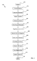
- FIG. 2 depicts a flow chart of a process for manufacturing a device with epitaxially grown piezoresistors in accordance with principles of the present invention
- FIG. 3 depicts a cross-sectional view of a substrate, which in this embodiment is a silicon on insulator (SOI) substrate, which may be used in a device in accordance with principles of the present invention
- FIG. 4 depicts a top plan view of the substrate of FIG. 3 with a photomask including windows having the shape of conductive traces to be implanted into the upper surface of the substrate;
- FIG. 5 depicts a cross sectional view of the substrate and photomask of FIG. 4 taken along the line A-A of FIG. 4 ;
- FIG. 6 depicts a cross sectional view of the substrate of FIG. 4 after impurities have been implanted and activated and a thin silicon oxide layer has been grown on the upper surface of the substrate;
- FIG. 7 depicts a top plan view of the substrate of FIG. 6 with a photomask including a window having the shape of a trench to be etched into the upper surface of the substrate;
- FIG. 8 depicts a cross sectional view of the substrate and photomask of FIG. 7 taken along the line B-B of FIG. 7 ;
- FIG. 9 depicts a top plan view of the substrate of FIG. 7 after a trench has been etched through the SOI active layer to the buried oxide layer and piezoresistive epitaxial single crystal silicon has been selectively deposited on the vertical walls of the SOI active layer exposed by the trench;
- FIG. 10 depicts a cross sectional view of the substrate of FIG. 9 taken along the line C-C of FIG. 9 ;
- FIG. 11 depicts a top plan view of the substrate of FIG. 9 the piezoresistive epitaxial single crystal silicon layer has been etched leaving two piezoresistive sensing elements positioned on the side walls of a tether area;
- FIG. 12 depicts a cross sectional view of the substrate of FIG. 11 taken along the line D-D of FIG. 11 ;
- FIG. 13 depicts a cross sectional view of the substrate of FIG. 11 after vapor etching has been used to remove portions of the buried oxide layer to create a void underneath the tether area and proof mass area;
- FIG. 14 depicts a top plan view of the substrate of FIG. 13 with a shadow mask including windows having the shape of a contact pads to be formed onto the upper surface of the substrate;
- FIG. 15 depicts a top plan view of the substrate of FIG. 14 with contact pads formed onto the upper surface of the substrate in electrically conductive contact with conductive traces in the upper surface of the substrate;
- FIG. 16 depicts a cross sectional view of the substrate of FIG. 15 taken along the line E-E of FIG. 15 ;
- FIG. 17 depicts a top plan view of an alternatively configured device formed in accordance with principles of the present invention configured with two accelerometers;
- FIG. 18 depicts a top plan view of an alternatively configured device formed in accordance with principles of the present invention configured with two accelerometers sharing a common proof mass;
- FIG. 19 depicts a top plan view of an alternatively configured device formed in accordance with principles of the present invention configured to provide three ranges of acceleration sensing.
- FIG. 1 depicts a perspective view of an accelerometer device 100 .
- the device 100 is formed on a substrate 102 , which, in this embodiment, is a silicon on insulator (SOI) substrate.
- the substrate 102 includes an SOI handle layer 104 , a buried oxide layer 106 and an SOI active layer 108 , which is shown partially cutaway for clarity of description.
- SOI silicon on insulator
- a trench 110 extends from the upper surface 112 of the SOI active layer 108 to a void area 114 between the SOI handle layer 104 and the SOI active layer 108 formed by removal of portions of the buried oxide layer 106 .
- the trench 110 circumscribes an anchor area 116 , which is connected to the SOI handle layer 104 by a remnant 118 of the buried oxide layer 106 .
- the contact pad 120 which in this embodiment is made of aluminum or could be another metal or conductive material, is in electrically conductive contact with a conductive trace 126 implanted or other conductive material such as metal or silicon in the SOI active layer 108 .
- the conductive trace 126 is in turn in electrically conductive contact with a piezoresistive sensing element 128 .
- the piezoresistive sensing element 128 extends along the length of a tether area (also referred to as a cantilever arm) 130 , extending outwardly from one side of the tether area 130 into the trench 110 .
- the contact pad 124 is in electrically conductive contact with a conductive trace 132 implanted or other conductive material such as metal or silicon in the SOI active layer 108 .
- the conductive trace 132 is in turn in electrically conductive contact with a piezoresistive sensing element 134 .
- the piezoresistive sensing element 134 extends along the length of a tether area 130 , extending outwardly from the opposite side of the tether area 130 into the trench 110 .
- the contact pad 122 is in electrically conductive contact with a conductive trace 138 implanted or other conductive material such as metal or silicon in the SOI active layer 108 .
- the conductive trace 138 includes an anchor portion 140 implanted or conductively doped or deposited in the anchor area 116 .
- An extension portion 142 of the conductive trace extends across the tether area 130 to a base section 144 .
- the base section 144 is implanted or conductively doped or deposited into a proof mass area 146 and is electrically conductively connected to the piezoresistive sensing element 128 and the piezoresistive sensing element 134 .
- the accelerometer device 100 is mounted to an object (not shown).
- the SOI handle layer 104 which is fixedly attached to the object (not shown), accelerates simultaneously with the object (not shown).
- the anchor area 116 is fixedly mounted on the SOI handle layer 104 through the remnant 118 . Accordingly, the anchor area 116 also accelerates simultaneously with the object (not shown).
- the proof mass area 146 and the tether area 130 are not fixedly mounted to the SOI handle layer 104 . Rather, the proof mass area 146 and the tether area 130 are supported by the anchor area 116 . Accordingly, as the anchor area 116 accelerates in the direction of the arrow 148 , the tether flexes because of the inertia of the tether area 130 and the proof mass area 146 . Flexure of the tether area 130 causes the piezoresistive sensing elements 128 and 134 to flex. The piezoresistive sensing elements 128 and 134 translate the mechanical movement of the flexure area into a resistance change.
- the conductive traces 126 , 132 , and 138 provide a conductive path for the current which translates the resistance change in the piezoresistive sensing element into a change in voltage across the sensing elements 128 and 134 , resulting in a voltage differential across the contact pads 120 , 122 and 126 .
- the resistance or voltage change may then be used to determine the acceleration of the object (not shown).
- FIG. 2 shows a flow chart 150 of a manufacturing process that may be used to produce the accelerometer device 100 .
- the process 150 of FIG. 2 begins (block 152 ) and a substrate is provided (block 154 ).
- a photomask defining low resistivity connection paths is then formed (block 156 ), followed by implantation of impurities to form the low resistivity paths (block 158 ).
- the implanted impurities are activated and a thin silicon dioxide layer is grown by thermal oxidation (block 160 ).
- a second photomask which is used to define an anchor, a tether and a proof mass in the thin silicon dioxide layer is formed (block 162 ) after which a deep reactive ion etch is used to create a trench from the upper surface of the substrate to a buried oxide layer of the substrate to form the anchor, tether and proof mass areas (block 164 ).
- Doped epitaxial single crystal silicon is selectively deposited on the silicon area exposed by the deep reactive ion etch (block 166 ).
- a third photomask is formed to protect the piezoresistive epitaxial single crystal silicon on the side wall area of the tether (block 168 ) and unprotected piezoresistive epitaxial single crystal silicon is etched off (block 170 ).
- Portions of the buried oxide layer are removed to release the proof mass and tether (block 172 ).
- a shadow mask is formed to define electrical contact pad areas (block 174 ) and aluminum is sputter deposited to form electrical contact areas (block 176 ). The process then ends (block 178 ).
- FIGS. 3-16 One example of the process of FIG. 2 is shown in FIGS. 3-16 .
- a substrate 200 is shown in FIG. 3 .
- the substrate 200 in this embodiment is a silicon on insulator (SOI) substrate including an SOI handle layer 202 , a buried silicon dioxide layer 204 and an active SOI layer 206 .
- SOI silicon on insulator
- a photomask 208 is formed on the exposed upper surface of the SOI active layer 206 as shown in FIGS. 4 and 5 .
- the photomask 208 includes windows 210 through which the active layer 206 is exposed. Impurities are then implanted through the windows 210 into the active layer 206 .
- Thermal oxidation is used to activate the impurities to form conductive traces 212 within the SOI active layer 206 and a thin silicon dioxide layer 214 , which covers the conductive, traces 212 and the SOI active layer 206 as shown in FIG. 6 .
- a photomask 220 shown in FIGS. 7 and 8 , is formed on the silicon oxide layer 214 .
- the photomask 220 includes a window 222 , which defines a fixed anchor area 224 , a tether area 226 and a proof mass area 228 .
- a trench 230 (see FIGS. 9 and 10 ) is then formed in the portion of the silicon dioxide layer 214 that is exposed through the window 222 , along with the portion of the SOI active layer 206 that is located directly below the exposed portion of the silicon dioxide layer 214 using a deep reactive ion etch process to expose the portion of the buried oxide layer 204 that is located directly below the exposed portion of the silicon dioxide layer 214 .
- a selective single crystal silicon layer 232 is then epitaxially deposited on the inner vertical surfaces of the SOI active layer 206 that are exposed by the trench 230 as shown in FIGS. 9 and 10 .
- the selective deposition of epitaxial silicon material also forms a single crystal silicon layer 234 on the outer vertical surfaces of the SOI active layer 206 that are exposed by the trench 230
- Photolithography is then used to protect the portions of the single crystal silicon layer 232 adjacent to the tether area 226 and the remainder of the single crystal silicon layer 232 and the single crystal silicon layer 234 are etched.
- the single crystal silicon layer 234 within the trench 230 is completely removed and the single crystal silicon layer 232 is removed with the exception of sensing elements 236 and 238 adjacent the tether area 226 .
- the sensing element 236 is electrically conductively connected to two of the traces 212 . Specifically, the sensing element 236 is conductively connected to an outer trace 240 , which is located in the anchor area 224 , and to an inner trace 242 .
- the inner trace 242 includes a base portion 244 located in the proof mass area 228 to which the sensing element 236 is conductively connected, an extension portion 246 which extends along the tether area 226 , and an end portion 248 located in the anchor area 224 .
- the sensing element 238 is also conductively connected to the base portion 244 .
- the sensing element 238 is further conductively connected to an outer trace 250 .
- a vapor phase hydrofluoric acid is then introduced through the trenches 230 to remove portions of the buried oxide layer 204 .
- the hydrofluoric acid etching creates void areas in the buried oxide layer 204 leaving the remnants 260 , 262 and 264 as shown in FIG. 13 .
- the remnant 262 supports the anchor area 224 on the SOI handle layer 202 .
- the tether area 226 and the proof mass area 228 are released from the SOI handle layer 202 as a void area in the buried oxide layer 204 separates the tether area 226 and the proof mass area 228 from the SOI handle layer 202 . Accordingly, the proof mass area 228 is supported by the tether area 226 , which acts as a cantilever arm supported by the anchor area 224 .
- a shadow mask 270 is formed on the SOI active layer 206 .
- the shadow mask 270 includes windows 272 , 274 , and 276 .
- Pad connection portions 278 , 280 , and 282 of outer trace 240 , inner trace 242 and outer trace 250 , respectively, are exposed though the windows 272 , 274 , and 276 .
- Aluminum or could be another metal or conductive material is sputter deposited onto the pad connection portions 278 , 280 , and 282 to form contact pads 284 , 286 , and 288 shown in FIGS. 15 and 16 .
- the device 300 of FIG. 17 includes two accelerometers 302 and 304 on a single substrate 306 .
- a single trench 308 defines both devices 302 and 304 .
- Each of the devices 302 and 304 are made in the same manner as the accelerometer 100 .
- an accelerometer 310 shown in FIG. 18 , includes a single proof mass 312 .
- Two cantilever arms 314 and 316 extending from two anchor areas 318 and 320 , respectively, support the proof mass 312 .
- Each of the anchor areas 318 and 320 include a set of contact pads 322 and 324 , respectively. The output from the contact pad sets 322 and 324 may be combined.
- one of the two cantilever arms 314 or 316 may be used as a primary sensor and the other of the two cantilever arms 314 or 316 used as a back-up sensor.
- a multiple range accelerometer 330 is made in substantially the same manner as the accelerometer 100 .
- the accelerometer 330 includes five cantilever arms 332 , 334 , 336 , 338 , and 340 .
- Each of the cantilever arms 332 , 334 , 336 , 338 , and 340 are conductively connected to a respective set of contact pads 342 , 344 , 346 , 348 or 350 located on a respective anchor area 352 , 354 , 356 , 358 or 360 .
- the cantilever arms 332 , 334 , 336 , 338 , and 340 support three proof masses 362 , 364 and 366 .
- the cantilever arms 332 and 338 support the proof mass 362
- the cantilever arms 334 and 336 support the proof mass 364
- the cantilever arm 340 supports the proof mass 366 .
- the proof mass 362 has the greatest mass of the proof masses 362 , 364 , and 366 while the proof mass 366 has the lowest mass.
- the inertia of the proof mass 362 is greater than the inertia of the proof mass 364 .
- the cantilever arms 332 and 338 will bend more than the cantilever arms 334 and 336 .
- the respective masses are selected such that each of the cantilever arms 332 , 334 , 336 , and 338 will bend more than the cantilever arm 340 .
- the device 330 thus provides an accelerometer, which can be wired to provide a high range output, a low range output and a medium range output.
- the device 330 is further configured to provide increased sensitivity for the medium range acceleration force output and low range acceleration force output. Specifically, the output from the contact pad sets 342 and 348 may be combined to provide increased sensitivity for the low range output while the contact pad sets 344 and 346 may be combined to provide increased sensitivity for the medium range output.
- more piezoresistors are combined to provide an output for a device.
- the cantilevers are not parallel.
- the response characteristics of a device in accordance with principles of the invention may be modified in other ways.
- the dimensions of the cantilever itself along with the possibility of different materials used in forming the cantilever may be selected to provide desired properties. Another use of these unreleased devices could be a temperature compensation reference device.
Abstract
Description
Claims (20)
Priority Applications (6)
| Application Number | Priority Date | Filing Date | Title |
|---|---|---|---|
| US12/353,080 US8187903B2 (en) | 2009-01-13 | 2009-01-13 | Method of epitaxially growing piezoresistors |
| EP10700463.2A EP2387722B1 (en) | 2009-01-13 | 2010-01-12 | Method of forming a device with a piezoresistor and accelerometer |
| CN201080008388.XA CN102326088B (en) | 2009-01-13 | 2010-01-12 | Method of forming device with piezoresistor and accelerometer |
| KR1020117018841A KR101654391B1 (en) | 2009-01-13 | 2010-01-12 | Method of forming a device with a piezoresistor |
| JP2011546301A JP5718253B2 (en) | 2009-01-13 | 2010-01-12 | Method of forming a device having a piezoresistor and an accelerometer |
| PCT/US2010/020750 WO2010083158A1 (en) | 2009-01-13 | 2010-01-12 | Method of forming a device with a piezoresistor and accelerometer |
Applications Claiming Priority (1)
| Application Number | Priority Date | Filing Date | Title |
|---|---|---|---|
| US12/353,080 US8187903B2 (en) | 2009-01-13 | 2009-01-13 | Method of epitaxially growing piezoresistors |
Publications (2)
| Publication Number | Publication Date |
|---|---|
| US20100176465A1 US20100176465A1 (en) | 2010-07-15 |
| US8187903B2 true US8187903B2 (en) | 2012-05-29 |
Family
ID=42046170
Family Applications (1)
| Application Number | Title | Priority Date | Filing Date |
|---|---|---|---|
| US12/353,080 Active 2029-10-21 US8187903B2 (en) | 2009-01-13 | 2009-01-13 | Method of epitaxially growing piezoresistors |
Country Status (6)
| Country | Link |
|---|---|
| US (1) | US8187903B2 (en) |
| EP (1) | EP2387722B1 (en) |
| JP (1) | JP5718253B2 (en) |
| KR (1) | KR101654391B1 (en) |
| CN (1) | CN102326088B (en) |
| WO (1) | WO2010083158A1 (en) |
Cited By (2)
| Publication number | Priority date | Publication date | Assignee | Title |
|---|---|---|---|---|
| US20120125117A1 (en) * | 2009-05-27 | 2012-05-24 | Frederic Njikam Njimonzie | Micromechanical component and production method for a micromechanical component |
| US20210356336A1 (en) * | 2020-05-14 | 2021-11-18 | Commissariat A L'energie Atomique Et Aux Energies Alternatives | Detection device using piezoresistive transduction |
Families Citing this family (7)
| Publication number | Priority date | Publication date | Assignee | Title |
|---|---|---|---|---|
| DE102010002992B4 (en) | 2010-03-18 | 2023-05-04 | Robert Bosch Gmbh | Piezoresistive micromechanical sensor component and corresponding manufacturing method |
| EP2697155B1 (en) * | 2011-04-14 | 2017-01-11 | Robert Bosch GmbH | Mems package or sensor package with intra-cap electrical via and method thereof |
| US8648432B2 (en) * | 2011-11-28 | 2014-02-11 | Texas Instruments Deutschland Gmbh | Fully embedded micromechanical device, system on chip and method for manufacturing the same |
| US8889451B2 (en) * | 2012-02-21 | 2014-11-18 | Freescale Semiconductor, Inc. | MEMS pressure transducer assembly and method of packaging same |
| CN107512699B (en) * | 2017-07-27 | 2019-10-11 | 沈阳工业大学 | SOI acceleration sensitive manufacturing method of chip based on bonding techniques |
| CN109087855A (en) * | 2018-07-24 | 2018-12-25 | 华东师范大学 | A kind of method of mixed structure edge protuberance in improvement SOI technology |
| CN111537396B (en) * | 2020-04-24 | 2021-02-19 | 西安交通大学 | Multi-operation-mode piezoelectric viscosity sensor chip and working method and preparation method thereof |
Citations (17)
| Publication number | Priority date | Publication date | Assignee | Title |
|---|---|---|---|---|
| US5500078A (en) | 1993-12-24 | 1996-03-19 | Kyung Pook National University Sensor Technology Research Center | 8-beam bridge-type silicon acceleration sensor and the fabricating method thereof |
| US5672551A (en) | 1994-03-18 | 1997-09-30 | The Foxboro Company | Method for manufacturing a semiconductor pressure sensor with single-crystal silicon diaphragm and single-crystal gage elements |
| US5856967A (en) | 1997-08-27 | 1999-01-05 | International Business Machines Corporation | Atomic force microscopy data storage system with tracking servo from lateral force-sensing cantilever |
| US5959200A (en) | 1997-08-27 | 1999-09-28 | The Board Of Trustees Of The Leland Stanford Junior University | Micromachined cantilever structure providing for independent multidimensional force sensing using high aspect ratio beams |
| US6025208A (en) * | 1997-08-27 | 2000-02-15 | The Board Of Trustees Of The Leland Stanford Junior University | Method of making electrical elements on the sidewalls of micromechanical structures |
| WO2000037912A1 (en) | 1998-12-18 | 2000-06-29 | Maxim Integrated Products, Inc. | Compensated semiconductor pressure sensor |
| US6096040A (en) | 1996-06-14 | 2000-08-01 | Depuy Ace Medical Company | Upper extremity bone plates |
| US6140143A (en) | 1992-02-10 | 2000-10-31 | Lucas Novasensor Inc. | Method of producing a buried boss diaphragm structure in silicon |
| US6278167B1 (en) | 1998-08-14 | 2001-08-21 | Infineon Technologies Ag | Semiconductor sensor with a base element and at least one deformation element |
| US6389899B1 (en) * | 1998-06-09 | 2002-05-21 | The Board Of Trustees Of The Leland Stanford Junior University | In-plane micromachined accelerometer and bridge circuit having same |
| WO2003023414A1 (en) | 2001-09-04 | 2003-03-20 | Tokyo Electron Limited | Microstructure with movable mass |
| EP1427010A1 (en) | 2002-11-29 | 2004-06-09 | STMicroelectronics S.r.l. | Manufacturing method for a semiconductor substrate comprising at least a buried cavity and devices formed with this method |
| US20040200281A1 (en) * | 2003-04-11 | 2004-10-14 | Kenny Thomas W. | Ultra-miniature accelerometers |
| US6897538B2 (en) | 2001-08-20 | 2005-05-24 | Honeywell International, Inc. | Micro-machined electromechanical system (MEMS) accelerometer device having arcuately shaped flexures |
| US20050266599A1 (en) | 2004-05-31 | 2005-12-01 | Naokatsu Ikegami | Method of manufacturing a micro-electrical-mechanical system |
| US20080227234A1 (en) | 2007-03-13 | 2008-09-18 | Oki Electric Industry Co., Ltd. | Method of manufacturing a semiconductor device |
| US7441440B2 (en) * | 2003-04-24 | 2008-10-28 | Sacmi Cooperativa Meccanici Imola Soc. Coop. A.R.L. | Thin semiconductor film gas sensor device |
Family Cites Families (5)
| Publication number | Priority date | Publication date | Assignee | Title |
|---|---|---|---|---|
| US3304787A (en) * | 1962-12-29 | 1967-02-21 | Toyoda Chuo Kenkyusho Kk | Three-dimensional accelerometer device |
| JPH04137671A (en) * | 1990-09-28 | 1992-05-12 | Yokogawa Electric Corp | Manufacture of semiconductor acceleration sensor |
| US5526112A (en) * | 1993-03-05 | 1996-06-11 | Sahagen; Armen N. | Probe for monitoring a fluid medium |
| JP2002323513A (en) * | 2001-02-23 | 2002-11-08 | Fuji Electric Co Ltd | Semiconductor device and manufacturing method for it |
| CN100363743C (en) * | 2005-09-12 | 2008-01-23 | 中北大学 | Resonance tunnel through pressure resistance type micro acceleration meter |
-
2009
- 2009-01-13 US US12/353,080 patent/US8187903B2/en active Active
-
2010
- 2010-01-12 CN CN201080008388.XA patent/CN102326088B/en active Active
- 2010-01-12 JP JP2011546301A patent/JP5718253B2/en active Active
- 2010-01-12 WO PCT/US2010/020750 patent/WO2010083158A1/en active Application Filing
- 2010-01-12 KR KR1020117018841A patent/KR101654391B1/en active IP Right Grant
- 2010-01-12 EP EP10700463.2A patent/EP2387722B1/en active Active
Patent Citations (18)
| Publication number | Priority date | Publication date | Assignee | Title |
|---|---|---|---|---|
| US6140143A (en) | 1992-02-10 | 2000-10-31 | Lucas Novasensor Inc. | Method of producing a buried boss diaphragm structure in silicon |
| US5500078A (en) | 1993-12-24 | 1996-03-19 | Kyung Pook National University Sensor Technology Research Center | 8-beam bridge-type silicon acceleration sensor and the fabricating method thereof |
| US5672551A (en) | 1994-03-18 | 1997-09-30 | The Foxboro Company | Method for manufacturing a semiconductor pressure sensor with single-crystal silicon diaphragm and single-crystal gage elements |
| US6096040A (en) | 1996-06-14 | 2000-08-01 | Depuy Ace Medical Company | Upper extremity bone plates |
| US5856967A (en) | 1997-08-27 | 1999-01-05 | International Business Machines Corporation | Atomic force microscopy data storage system with tracking servo from lateral force-sensing cantilever |
| US5959200A (en) | 1997-08-27 | 1999-09-28 | The Board Of Trustees Of The Leland Stanford Junior University | Micromachined cantilever structure providing for independent multidimensional force sensing using high aspect ratio beams |
| US6025208A (en) * | 1997-08-27 | 2000-02-15 | The Board Of Trustees Of The Leland Stanford Junior University | Method of making electrical elements on the sidewalls of micromechanical structures |
| US6389899B1 (en) * | 1998-06-09 | 2002-05-21 | The Board Of Trustees Of The Leland Stanford Junior University | In-plane micromachined accelerometer and bridge circuit having same |
| US6278167B1 (en) | 1998-08-14 | 2001-08-21 | Infineon Technologies Ag | Semiconductor sensor with a base element and at least one deformation element |
| WO2000037912A1 (en) | 1998-12-18 | 2000-06-29 | Maxim Integrated Products, Inc. | Compensated semiconductor pressure sensor |
| US6897538B2 (en) | 2001-08-20 | 2005-05-24 | Honeywell International, Inc. | Micro-machined electromechanical system (MEMS) accelerometer device having arcuately shaped flexures |
| US6991957B2 (en) | 2001-08-20 | 2006-01-31 | Honeywell International, Inc. | Micro-machined electromechanical system (MEMS) accelerometer device having arcuately shaped flexures |
| WO2003023414A1 (en) | 2001-09-04 | 2003-03-20 | Tokyo Electron Limited | Microstructure with movable mass |
| EP1427010A1 (en) | 2002-11-29 | 2004-06-09 | STMicroelectronics S.r.l. | Manufacturing method for a semiconductor substrate comprising at least a buried cavity and devices formed with this method |
| US20040200281A1 (en) * | 2003-04-11 | 2004-10-14 | Kenny Thomas W. | Ultra-miniature accelerometers |
| US7441440B2 (en) * | 2003-04-24 | 2008-10-28 | Sacmi Cooperativa Meccanici Imola Soc. Coop. A.R.L. | Thin semiconductor film gas sensor device |
| US20050266599A1 (en) | 2004-05-31 | 2005-12-01 | Naokatsu Ikegami | Method of manufacturing a micro-electrical-mechanical system |
| US20080227234A1 (en) | 2007-03-13 | 2008-09-18 | Oki Electric Industry Co., Ltd. | Method of manufacturing a semiconductor device |
Non-Patent Citations (3)
| Title |
|---|
| Gwiy-Sang Chung, Fabrication and Characteristics of Si Piezoresistive Micropressure Sensors for Tactile Imaging Devices (2006), Journal of the Korean Physical Society, vol. 49, No. 1, Jul. 2006, pp. 37-41 (5 pages). |
| International Search Report in corresponding PCT application (i.e., PCT/US2010/020750), mailed Apr. 13, 2010 (4 pages). |
| Jessica Arlett, Properties of piezoresistive silicon nano-scale cantilevers with applications to BioNEMS (2006) (unpublished Ph.D. dissertation, California Institute of Technology) (on file with author) (8 pages). |
Cited By (3)
| Publication number | Priority date | Publication date | Assignee | Title |
|---|---|---|---|---|
| US20120125117A1 (en) * | 2009-05-27 | 2012-05-24 | Frederic Njikam Njimonzie | Micromechanical component and production method for a micromechanical component |
| US8813573B2 (en) * | 2009-05-27 | 2014-08-26 | Robert Bosch Gmbh | Micromechanical component and production method for a micromechanical component |
| US20210356336A1 (en) * | 2020-05-14 | 2021-11-18 | Commissariat A L'energie Atomique Et Aux Energies Alternatives | Detection device using piezoresistive transduction |
Also Published As
| Publication number | Publication date |
|---|---|
| JP5718253B2 (en) | 2015-05-13 |
| JP2012515348A (en) | 2012-07-05 |
| EP2387722A1 (en) | 2011-11-23 |
| KR20110104997A (en) | 2011-09-23 |
| KR101654391B1 (en) | 2016-09-05 |
| US20100176465A1 (en) | 2010-07-15 |
| CN102326088B (en) | 2017-04-19 |
| WO2010083158A1 (en) | 2010-07-22 |
| EP2387722B1 (en) | 2020-03-11 |
| CN102326088A (en) | 2012-01-18 |
Similar Documents
| Publication | Publication Date | Title |
|---|---|---|
| US8187903B2 (en) | Method of epitaxially growing piezoresistors | |
| US9061895B2 (en) | Micromechanical structure comprising a mobile part having stops for out-of plane displacements of the structure and its production process | |
| US7268463B2 (en) | Stress release mechanism in MEMS device and method of making same | |
| US4553436A (en) | Silicon accelerometer | |
| US8810030B2 (en) | MEMS device with stress isolation and method of fabrication | |
| US7736931B1 (en) | Wafer process flow for a high performance MEMS accelerometer | |
| US9573799B2 (en) | MEMS device having variable gap width and method of manufacture | |
| EP3052901B1 (en) | Inertial and pressure sensors on single chip | |
| EP0913921A1 (en) | Method for manufacturing a semiconductor material integrated micractuator, in particular for a hard disc mobile read/write head, and a microactuator obtained thereby | |
| US20120031186A1 (en) | Inertial sensor and method for manufacturing an inertial sensor | |
| US9745189B1 (en) | MEMS device with isolation sub-frame structure | |
| KR20170002947A (en) | Pressure sensor element and method for manufacturing same | |
| US8680631B2 (en) | High aspect ratio capacitively coupled MEMS devices | |
| US6215645B1 (en) | Differential capacitor structure | |
| CN214122270U (en) | Micro-electromechanical sensor | |
| JP4220582B2 (en) | Sensor manufacturing method | |
| US8430255B2 (en) | Method of accurately spacing Z-axis electrode | |
| CN111308126A (en) | Capacitive triaxial accelerometer with mass block increased and manufacturing method thereof | |
| CN214122269U (en) | Micro-electromechanical sensor | |
| CN112327003A (en) | Micro-electromechanical sensor and method for manufacturing the same | |
| CN116430072A (en) | MEMS piezoresistive accelerometer chip with position-independent pure axial deformation piezoresistive beams and preparation method thereof |
Legal Events
| Date | Code | Title | Description |
|---|---|---|---|
| AS | Assignment |
Owner name: OFFICE OF TECHNOLOGY LICENSING, STANFORD UNIVERSIT Free format text: ASSIGNMENT OF ASSIGNORS INTEREST;ASSIGNORS:YAMA, GARY;PRUITT, BETH;BARLIAN, ARNOLDUS ALVIN;SIGNING DATES FROM 20081126 TO 20090105;REEL/FRAME:022100/0755 Owner name: ROBERT BOSCH GMBH, GERMANY Free format text: ASSIGNMENT OF ASSIGNORS INTEREST;ASSIGNORS:YAMA, GARY;PRUITT, BETH;BARLIAN, ARNOLDUS ALVIN;SIGNING DATES FROM 20081126 TO 20090105;REEL/FRAME:022100/0755 |
|
| AS | Assignment |
Owner name: NATIONAL SCIENCE FOUNDATION, VIRGINIA Free format text: CONFIRMATORY LICENSE;ASSIGNOR:STANFORD UNIVERSITY;REEL/FRAME:024570/0697 Effective date: 20100618 |
|
| STCF | Information on status: patent grant |
Free format text: PATENTED CASE |
|
| FPAY | Fee payment |
Year of fee payment: 4 |
|
| MAFP | Maintenance fee payment |
Free format text: PAYMENT OF MAINTENANCE FEE, 8TH YEAR, LARGE ENTITY (ORIGINAL EVENT CODE: M1552); ENTITY STATUS OF PATENT OWNER: LARGE ENTITY Year of fee payment: 8 |
|
| MAFP | Maintenance fee payment |
Free format text: PAYMENT OF MAINTENANCE FEE, 12TH YEAR, LARGE ENTITY (ORIGINAL EVENT CODE: M1553); ENTITY STATUS OF PATENT OWNER: LARGE ENTITY Year of fee payment: 12 |