US8202382B2 - Method for manufacturing micro movable element - Google Patents
Method for manufacturing micro movable element Download PDFInfo
- Publication number
- US8202382B2 US8202382B2 US12/509,584 US50958409A US8202382B2 US 8202382 B2 US8202382 B2 US 8202382B2 US 50958409 A US50958409 A US 50958409A US 8202382 B2 US8202382 B2 US 8202382B2
- Authority
- US
- United States
- Prior art keywords
- section
- frame
- layer
- movable element
- micro movable
- Prior art date
- Legal status (The legal status is an assumption and is not a legal conclusion. Google has not performed a legal analysis and makes no representation as to the accuracy of the status listed.)
- Expired - Fee Related, expires
Links
Images


Classifications
-
- B—PERFORMING OPERATIONS; TRANSPORTING
- B81—MICROSTRUCTURAL TECHNOLOGY
- B81C—PROCESSES OR APPARATUS SPECIALLY ADAPTED FOR THE MANUFACTURE OR TREATMENT OF MICROSTRUCTURAL DEVICES OR SYSTEMS
- B81C1/00—Manufacture or treatment of devices or systems in or on a substrate
- B81C1/00777—Preserve existing structures from alteration, e.g. temporary protection during manufacturing
- B81C1/00825—Protect against mechanical threats, e.g. against shocks, or residues
-
- G—PHYSICS
- G02—OPTICS
- G02B—OPTICAL ELEMENTS, SYSTEMS OR APPARATUS
- G02B26/00—Optical devices or arrangements for the control of light using movable or deformable optical elements
- G02B26/08—Optical devices or arrangements for the control of light using movable or deformable optical elements for controlling the direction of light
- G02B26/0816—Optical devices or arrangements for the control of light using movable or deformable optical elements for controlling the direction of light by means of one or more reflecting elements
- G02B26/0833—Optical devices or arrangements for the control of light using movable or deformable optical elements for controlling the direction of light by means of one or more reflecting elements the reflecting element being a micromechanical device, e.g. a MEMS mirror, DMD
- G02B26/0841—Optical devices or arrangements for the control of light using movable or deformable optical elements for controlling the direction of light by means of one or more reflecting elements the reflecting element being a micromechanical device, e.g. a MEMS mirror, DMD the reflecting element being moved or deformed by electrostatic means
-
- G—PHYSICS
- G02—OPTICS
- G02B—OPTICAL ELEMENTS, SYSTEMS OR APPARATUS
- G02B6/00—Light guides; Structural details of arrangements comprising light guides and other optical elements, e.g. couplings
- G02B6/24—Coupling light guides
- G02B6/26—Optical coupling means
- G02B6/35—Optical coupling means having switching means
- G02B6/351—Optical coupling means having switching means involving stationary waveguides with moving interposed optical elements
- G02B6/3512—Optical coupling means having switching means involving stationary waveguides with moving interposed optical elements the optical element being reflective, e.g. mirror
- G02B6/3518—Optical coupling means having switching means involving stationary waveguides with moving interposed optical elements the optical element being reflective, e.g. mirror the reflective optical element being an intrinsic part of a MEMS device, i.e. fabricated together with the MEMS device
-
- G—PHYSICS
- G02—OPTICS
- G02B—OPTICAL ELEMENTS, SYSTEMS OR APPARATUS
- G02B6/00—Light guides; Structural details of arrangements comprising light guides and other optical elements, e.g. couplings
- G02B6/24—Coupling light guides
- G02B6/26—Optical coupling means
- G02B6/35—Optical coupling means having switching means
- G02B6/354—Switching arrangements, i.e. number of input/output ports and interconnection types
- G02B6/3554—3D constellations, i.e. with switching elements and switched beams located in a volume
- G02B6/3556—NxM switch, i.e. regular arrays of switches elements of matrix type constellation
-
- B—PERFORMING OPERATIONS; TRANSPORTING
- B81—MICROSTRUCTURAL TECHNOLOGY
- B81B—MICROSTRUCTURAL DEVICES OR SYSTEMS, e.g. MICROMECHANICAL DEVICES
- B81B2201/00—Specific applications of microelectromechanical systems
- B81B2201/04—Optical MEMS
- B81B2201/042—Micromirrors, not used as optical switches
-
- B—PERFORMING OPERATIONS; TRANSPORTING
- B81—MICROSTRUCTURAL TECHNOLOGY
- B81B—MICROSTRUCTURAL DEVICES OR SYSTEMS, e.g. MICROMECHANICAL DEVICES
- B81B2203/00—Basic microelectromechanical structures
- B81B2203/01—Suspended structures, i.e. structures allowing a movement
- B81B2203/0145—Flexible holders
- B81B2203/0154—Torsion bars
-
- H—ELECTRICITY
- H04—ELECTRIC COMMUNICATION TECHNIQUE
- H04Q—SELECTING
- H04Q2213/00—Indexing scheme relating to selecting arrangements in general and for multiplex systems
- H04Q2213/13003—Constructional details of switching devices
Definitions
- the embodiments and examples thereof as discussed herein are related to a method for manufacturing a micro movable element including a minute movable section.
- micromovable elements having a minute structure formed by micromachining technology have been put to practical use in various technical fields.
- examples of such elements include a micro movable element having a minute oscillating section or a vibrating section, such as a micromirror element, an angular velocity sensor, and an acceleration sensor.
- a micromirror element is utilized as an element bearing a light reflection function in the technical fields of optical disks or optical telecommunications, for example.
- An angular velocity sensor and an acceleration sensor are utilized in a video camera or a camera phone as an image stabilizing function, in a car navigation system, an airbag inflation timing system, or a posture controlling system of a car or a robot, for example.
- JP-A-2003-19700, JP-A-2004-341364, and JP-A-2006-72252 disclosed such micro movable elements.
- a method for manufacturing a micro movable element that includes: forming a movable section, a frame, and a connecting section connecting the movable section with the frame on a substrate; bonding a film to a surface of the substrate in forming the movable section, the frame, and the connecting section; and patterning the film to form a support structure being bridged between the movable section and the frame.
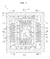
- FIG. 1 is a plan view of a micro movable element in an example of an embodiment
- FIG. 2 is a plan view partially illustrating the micro movable element illustrated in FIG. 1 ;
- FIG. 3 is a cross sectional view taken along line III-III of FIG. 1 ;
- FIG. 4 is a cross sectional view taken along line IV-IV of FIG. 1 ;
- FIG. 5 is a cross sectional view taken along line V-V of FIG. 1 ;
- FIG. 6 is a cross sectional view taken along line VI-VI of FIG. 1 ;
- FIG. 7 is a cross sectional view taken along line VII-VII of FIG. 1 ;
- FIG. 8 is a cross sectional view taken along line VIII-VIII of FIG. 1 ;
- FIGS. 9A to 9C illustrate manufacturing process of the micro movable element illustrated in FIG. 1 ;
- FIGS. 10A to 10C illustrate manufacturing process of the micro movable element subsequent to the manufacturing process illustrated in FIG. 9C ;
- FIGS. 11A to 11C illustrate manufacturing process of the micro movable element subsequent to the manufacturing process illustrated in FIG. 10C ;
- FIGS. 12A and 12B illustrate manufacturing process of the micro movable element subsequent to the manufacturing process illustrated in FIG. 11C ;
- FIGS. 13A to 13C illustrate manufacturing process of the micro movable element subsequent to the manufacturing process illustrated in FIG. 12B ;
- FIGS. 14A to 14D illustrate an assembly process according to an example of an embodiment
- FIG. 15 illustrates a support beam cutting process according to an example of an embodiment
- FIG. 16 is a schematic view of an optical switching device in another example of an embodiment.
- FIG. 17 is a schematic view of an optical switching device in still another example of an embodiment.
- FIGS. 1 to 8 illustrate a micro movable element X according to one example.
- FIG. 1 is a plan view of the micro movable element X.
- FIG. 2 is a plan view partially illustrating the micro movable element X.
- FIGS. 3 to 8 are cross sectional views respectively taken along lines III-III, IV-IV, V-V, VI-VI, VII-VII, and VIII-VIII of FIG. 1 .
- the micro movable element X includes an oscillation section 10 , a frame 20 , a frame 30 , a pair of torsion bars 40 , a pair of torsion bars 50 , comb electrodes 61 , 62 , 63 , 64 , 65 , 66 , 67 , and 68 , and support beams 71 and 72 .
- the micro movable element X is applied to a micromirror element with support beams.
- the micro movable element X is manufactured by processing a material substrate by bulk micromachining technology such as MEMS technology. As a material substrate, the so-called silicon on insulator (SOI) wafer is used.
- the material substrate has a laminated structure including a first silicon layer, a second silicon layer, and an insulating layer between the first and second silicon layers. Conductivity is imparted to the first and second silicon layers by doping an impurity.
- Each of the parts in the micro movable element X is derived and formed mainly from the first silicon layer or the second silicon layer. Accordingly, in view of the clarification of the drawing, parts which are derived from the first silicon layer and project closer to the viewer of the drawing than the insulating layer are marked with diagonal lines in FIG. 1 .
- the structure illustrated in FIG. 2 is derived from the second silicon layer in the micro movable element X.
- the oscillation section 10 is a part derived from the first silicon layer.
- a mirror surface 11 having a light reflecting function is disposed on the surface of the oscillation section 10 .
- a length W illustrated in FIG. 1 is from 20 to 300 ⁇ m, for example.
- the frame 20 is an inner frame having a shape surrounding the oscillation section 10 .
- the frame 20 has a laminated structure including a first layer section 21 derived from the first silicon layer, a second layer section 22 derived from the second silicon layer, and an insulating layer 23 between the first and second layer sections 21 and 22 .
- the second layer section 22 includes sections 22 a and 22 b .
- the first layer section 21 and the second layer section 22 are electrically separated from each other by the insulating layer 23 .
- the frame 30 is an outer frame having a shape surrounding the frame 20 .
- the frame 30 has a laminated structure including a first layer section 31 derived from the first silicon layer, a second layer section 32 derived from the second silicon layer, and an insulating layer 33 between the first and second layer sections 31 and 32 .
- the second layer section 32 includes sections 32 a , 32 b , 32 c , 32 d , and 32 e which are apart from one another via gaps.
- the first layer section 31 and the sections 32 a , 32 b , 32 c , and 32 d of the second layer section 32 are electrically separated from each other by the insulating layer 33 .
- the first layer section 31 and each of the sections 32 e of the second layer section 32 are electrically connected to each other via a conductive via 34 penetrating through the insulating layer 33 .
- an electrode pad 35 a is disposed on the surface of the section 32 a in the second layer section 32 .
- An electrode pad 35 b is disposed on the surface of the section 32 b .
- an electrode pad 35 c is disposed on the surface of the section 32 c .
- An electrode pad 35 d is disposed on the surface of the section 32 d .
- an electrode pad 35 e is disposed on the surface of each of the sections 32 e.
- Each of the pair of torsion bars 40 is a part derived from the first silicon layer.
- the pair of torsion bars 40 are connected to the oscillation section 10 and the first layer section 21 of the frame 20 .
- the oscillation section 10 and the frame 20 are connected to each other.
- the oscillation section 10 and the first layer section 21 are electrically connected to each other by the torsion bars 40 .
- the torsion bars 40 are thinner than the oscillation section 10 and thinner than the first layer section 21 of the frame 20 in a thickness direction H of the element.
- the pair of torsion bars 40 define an axial center A 1 of the oscillating operation of the oscillation section 10 .
- each of the pair of torsion bars 50 has a laminated structure including a first layer section 51 derived from the first silicon layer, a second layer section 52 derived from the second silicon layer, and an insulating layer 53 between the first and second layer sections 51 and 52 .
- the pair of torsion bars 50 connects the frame 20 with the frame 30 .
- the first layer section 51 is connected to the first layer section 21 of the frame 20 and the first layer section 31 of the frame 30 .
- the first layer sections 21 and 31 are electrically connected to each other.
- the second layer section 52 is connected to the section 22 a of the second layer section 22 of the frame 20 and the section 32 a of the second layer section 32 of the frame 30 .
- the sections 22 a and 32 a are electrically connected to each other.
- the first layer section 51 is connected to the first layer section 21 of the frame 20 and the first layer section 31 of the frame 30 .
- the first layer sections 21 and 31 are electrically connected to each other.
- the second layer section 52 is connected to the section 22 b of the second layer section 22 of the frame 20 and the section 32 b of the second layer section 32 of the frame 30 .
- the sections 22 b and 32 b are electrically connected to each other.
- Each of the first layer sections 51 of the torsion bars 50 is thinner than the first layer section 21 of the frame 20 and thinner than the first layer section 31 of the frame 30 in the element thickness direction H.
- each of the second layer sections 52 of the torsion bars 50 is thinner than the second layer section 22 of the frame 20 and thinner than the second layer section 32 of the frame 30 in the element thickness direction H.
- the pair of torsion bars 50 define an axial center A 2 of the oscillating operation of the frame 20 and the oscillation section 10 . Also, the axial center A 2 is perpendicular to the axial center A 1 .
- the comb electrode 61 is a part derived from the first silicon layer. As illustrated in FIGS. 1 and 5 , the comb electrode 61 includes a plurality of electrode teeth 61 a . The plurality of electrode teeth 61 a extend from the oscillation section 10 in a direction perpendicular to the axial center A 1 and in parallel with one another.
- the comb electrode 62 is a part derived from the first silicon layer. As illustrated in FIGS. 1 and 6 , the comb electrode 62 includes a plurality of electrode teeth 62 a .
- the plurality of electrode teeth 62 a extend from the oscillation section 10 to the side opposite to the electrode teeth 61 a in a direction perpendicular to the axial center A 1 and in parallel with one another.
- the comb electrode 63 is a part derived from the second silicon layer. As illustrated in FIGS. 1 , 2 , and 5 , the comb electrode 63 includes a plurality of electrode teeth 63 a .
- the plurality of electrode teeth 63 a extend from the section 22 a of the second layer section 22 of the frame 20 to the side of the oscillation section 10 or the comb electrode 61 in a direction perpendicular to the axial center A 1 and in parallel with one another.
- the comb electrode 63 serves as an actuator of the element in cooperation with the comb electrode 61 .
- the comb electrode 64 is a part derived from the second silicon layer. As illustrated in FIGS. 1 , 2 , and 6 , the comb electrode 64 includes a plurality of electrode teeth 64 a .
- the plurality of electrode teeth 64 a extend from the section 22 b of the second layer section 22 of the frame 20 to the side of the oscillation section 10 or the comb electrode 62 in a direction perpendicular to the axial center A 1 and in parallel with one another.
- the comb electrode 64 serves as an actuator of the element in cooperation with the comb electrode 62 .
- the comb electrode 65 is a part derived from the first silicon layer. As illustrated in FIGS. 1 and 7 , the comb electrode 65 includes a plurality of electrode teeth 65 a .
- the plurality of electrode teeth 65 a extend from the first layer section 21 of the frame 20 to the side opposite to the oscillation section 10 in a direction perpendicular to the axial center A 2 and in parallel with one another.
- the comb electrode 66 is a part derived from the first silicon layer. As illustrated in FIGS. 1 and 8 , the comb electrode 66 includes a plurality of electrode teeth 66 a . The plurality of electrode teeth 66 a extend from the first layer section 21 of the frame 20 to the side opposite to the oscillation section 10 in a direction perpendicular to the axial center A 2 and in parallel with one another.
- the comb electrode 67 is a part derived from the second silicon layer. As illustrated in FIGS. 1 , 2 , and 7 , the comb electrode 67 includes a plurality of electrode teeth 67 a .
- the plurality of electrode teeth 67 a extend from the section 32 c of the second layer section 32 of the frame 30 to the side of the frame 20 or the comb electrode 65 in a direction perpendicular to the axial center A 2 and in parallel with one another.
- the comb electrode 67 serves as an actuator of the element in cooperation with the comb electrode 65 .
- the comb electrode 68 is a part derived from the second silicon layer. As illustrated in FIGS. 1 , 2 , and 8 , the comb electrode 68 includes a plurality of electrode teeth 68 a .
- the plurality of electrode teeth 68 a extend from the section 32 d of the second layer section 32 of the frame 30 to the side of the frame 20 or the comb electrode 66 in a direction perpendicular to the axial center A 2 and in parallel with one another.
- the comb electrode 68 serves as an actuator of the element in cooperation with the comb electrode 66 .
- the support beam 71 temporarily fixes the oscillation section 10 to the frame 20 in order to prevent or at least reduce damage to the torsion bars 40 .
- the support beam 71 is bridged between the oscillation section 10 and the frame 20 on the surface on the first silicon layer side.
- the support beam 71 reinforces the connection between the oscillation section 10 and the frame 20 due to the pair of torsion bars 40 until the support beam 71 is cut.
- the support beam 71 is cut or removed before the use of the micro movable element X.
- the support beam 71 is preferably made of an insulating material.
- the support beam 72 temporarily fixes the frame 20 to the frame 30 in order to prevent or at least reduce damage to the torsion bars 50 .
- the support beam 72 is bridged between the frame 20 and the frame 30 on the surface on the first silicon layer side.
- the support beam 72 reinforces the connection between the frames 20 and 30 due to the pair of torsion bars 50 until the support beam 72 is cut.
- the support beam 72 is cut or removed before the use of the micro movable element X.
- the support beam 72 is preferably made of an insulating material.
- FIGS. 9A to 13C illustrate manufacturing process of the micro movable element X.
- the method is one technique for manufacturing the micro movable element X by micromachining technology.
- the forming process of an oscillation section M, frames F 1 , F 2 , F 3 , F 4 , and F 5 , torsion bars T 1 , T 2 , and T 3 , a set of comb electrodes E 1 and E 2 , and support beams S 1 and S 2 , illustrated in FIG. 13C is illustrated as change in one cross section.
- the oscillation section M corresponds to a part of the oscillation section 10 .
- the frames F 1 , F 2 , and F 4 correspond to the frame 20 .
- the frames F 3 and F 5 correspond to the frame 30 .
- the torsion bar T 1 corresponds to the torsion bar 40 .
- the torsion bar T 2 corresponds to the torsion bar 40 .
- the torsion bar T 3 corresponds to the torsion bar 50 .
- the comb electrode E 1 corresponds to the comb electrodes 61 , 62 , 65 , and 66 .
- the comb electrode E 2 corresponds to the comb electrodes 63 , 64 , 67 , and 68 .
- the support beam S 1 corresponds to the support beam 71 .
- the support beam S 2 corresponds to the support beam 72 .
- a material substrate 100 illustrated in FIG. 9A is prepared.
- the material substrate 100 has a laminated structure including a silicon layer 101 , a silicon layer 102 , and an insulating layer 103 between the silicon layers 101 and 102 .
- a silicon on insulator (SOI) wafer is used as the material substrate 100 .
- a conductive via which is to serve as the conductive via 34 later is previously buried and formed in the material substrate 100 at predetermined places.
- Conductivity is imparted to the silicon layers 101 and 102 by doping an impurity.
- an impurity a p-type impurity such as B or an n-type impurity such as P or Sb is employed.
- silicon oxide is used for the insulating layer 103 .
- the thickness of the silicon layer 101 is from 10 to 100 ⁇ m, for example.
- the thickness of the silicon layer 102 is from 100 to 500 ⁇ m, for example.
- the thickness of the insulating layer 103 is from 0.2 to 2 ⁇ m, for example.
- a mirror surface 11 is formed on the silicon layer 101 .
- Electrode pads 35 are formed on the silicon layer 102 .
- the electrode pads 35 correspond to the electrode pads 35 a , 35 b , 35 c , 35 d , and 35 e .
- a metal film such as of Cr (50 nm) and a metal film such as of Au (200 nm) are deposited in sequence on the silicon layer 101 by sputtering.
- an etching process is sequentially performed on these metal films via a mask.
- the mirror surface 11 is formed on the silicon layer 101 .
- etching solution for Au for example, potassium iodide-iodine aqueous solution is used.
- etching solution for Cr for example, di-ammonium cerium nitrate aqueous solution is used.
- the electrode pads 35 are formed in substantially the same manner as the mirror surface 11 , for example.
- an oxide film pattern 110 and a resist pattern 111 are formed on the silicon layer 101 .
- An oxide film pattern 112 and a resist pattern 113 are formed on the silicon layer 102 .
- the oxide film pattern 110 has a pattern shape corresponding to the oscillation section M, the frames F 1 , F 2 , F 3 , F 4 , and F 5 , and the comb electrode E 1 .
- the resist pattern 111 has a pattern shape corresponding to the torsion bars T 1 , T 2 , and T 3 .
- the oxide film pattern 112 has a pattern shape corresponding to the frames F 1 , F 3 , F 4 , and F 5 and the comb electrode E 2 .
- the resist pattern 113 has a pattern shape corresponding to the torsion bar T 3 .
- the oxide film pattern 110 In the formation of the oxide film pattern 110 , first, an oxide film such as of silicon dioxide is deposited on the surface of the silicon layer 101 by a CVD method, for example. The thickness of the oxide film is 1 ⁇ m, for example. Next, the oxide film is patterned by etching using a resist pattern as a mask. The oxide film pattern 112 is also formed by a method equivalent to that of the oxide film pattern 110 . On the other hand, in the formation of the resist pattern 111 , first, a liquid photoresist is deposited on the silicon layer 101 by spin coating. Next, through an exposure process and a subsequent development process, the photoresist film is patterned.
- a liquid photoresist is deposited on the silicon layer 101 by spin coating. Next, through an exposure process and a subsequent development process, the photoresist film is patterned.
- AZP4210 manufactured by AZ Electronic Materials
- AZ1500 manufactured by AZ Electronic Materials
- the resist pattern 113 is also formed by a method equivalent to that of the resist pattern 111 .
- anisotropic dry etching is performed on the silicon layer 101 to a predetermined depth by deep reactive ion etching (DRIE) using the oxide film pattern 110 and the resist pattern 111 as masks.
- the predetermined depth corresponds to the thickness of the torsion bars T 1 and T 2 and a part of the torsion bar T 3 (the first layer section 51 ), which is 5 ⁇ m, for example.
- an etching apparatus equipped with a vacuum chamber is used to perform DRIE in the vacuum chamber under predetermined vacuum conditions.
- DRIE the so-called Bosch process in which etching and side-wall protection are alternatively performed may be used.
- a favorable anisotropic etching process may be performed by using the Bosch process.
- an anisotropic dry etching process is performed on the silicon layer 102 to a predetermined depth by DRIE using the oxide film pattern 112 and the resist pattern 113 as masks.
- the predetermined depth corresponds to the thickness of a part of the torsion bar T 3 (the first layer section 52 ), which is 5 ⁇ m, for example.
- the resist patterns 111 and 113 are peeled off by supplying a remover.
- a remover for example, AZ remover 700 (manufactured by AZ Electronic Materials) is used.
- anisotropic etching is performed on the silicon layer 101 until it reaches the insulating layer 103 by DRIE using the oxide film pattern 110 as a mask.
- the torsion bars T 1 and T 2 and the part of the torsion bar T 3 (the first layer section 51 ) which are thin and in contact with the insulating layer 103 are left.
- the oscillation section M, parts of the frames F 1 , F 3 , F 4 , and F 5 , the frame F 2 , the part of the torsion bar T 3 , and the comb electrode E 1 are formed in addition to the torsion bars T 1 and T 2 .
- a film material 114 is bonded to the material substrate 100 on the silicon layer 101 side by using a laminator or a bonding apparatus.
- a photosensitive film such as SU-8 3000 Film (manufactured by KAYAKU MICROCHEM) or TMMR (F) S2000 (manufactured by TOKYO OHKA KOGYO) is employed.
- the film material 114 is patterned to form the support beams S 1 and S 2 .
- the support beams S 1 and S 2 are formed by an exposure process and a subsequent development process.
- SU-8 Developer manufactured by KAYAKU MICROCHEM
- PM Thinner manufactured by TOKYO OHKA KOGYO
- a predetermined resist pattern is formed on the film material 114 in the process.
- the film material 114 is patterned by wet etching or dry etching using the resist pattern as a mask.
- a sub-carrier 116 is bonded to the material substrate 100 on the silicon layer 101 side via a bonding material 115 .
- a bonding material 115 for example, a silicon substrate, a quartz substrate or a metal substrate is used.
- the bonding material 115 for example, a resist, a thermoconductive grease, a sealant or a tape is used. Specific examples of the bonding material 115 include WAFERBOND (manufactured by Brewer Science, Inc.). In the process, the material substrate 100 and the sub-carrier 116 are bonded to each other under heat and pressure.
- the purpose for bonding the sub-carrier 116 as described above is to prevent or avert damage to the material substrate 100 or an etching apparatus in the next process.
- the next process in which etching is applied to the silicon layer 102 in a vacuum chamber of an etching apparatus because not only the silicon layer 101 which has been already subjected to etching but also the silicon layer 102 is subjected to etching, the mechanical strength of the material substrate 100 is greatly reduced.
- the sub-carrier 116 prevents or averts damage of the material substrate 100 as a reinforcing material for the material substrate 100 . Assuming that the material substrate 100 is damaged in a vacuum chamber, an etching apparatus is sometimes damaged by a broken piece of the material substrate 100 . Also in this case, the sub-carrier 116 which prevents or averts the damage of the material substrate 100 contributes to prevent or avert the damage of the apparatus.
- an anisotropic etching process is performed on the silicon layer 102 until it reaches the insulating layer 103 by DRIE using the oxide film pattern 112 as a mask.
- the part of the torsion bar T 3 (the second layer section 52 ) which is thin and in contact with the insulating layer 103 is left.
- parts of the frames F 1 , F 3 , F 4 , and F 5 and the comb electrode E 2 are formed in addition to the part of the torsion bar T 3 .
- the sub-carrier 116 is removed from the material substrate 100 .
- WAFERBOND manufactured by Brewer Science, Inc.
- the material substrate 100 and the sub-carrier 116 may be separated from each other by supplying WAFERBOND Remover (manufactured by Brewer Science, Inc.) to the bonding material 115 , for example.
- etching As illustrated in FIG. 13C , next, parts exposed on the oxide film patterns 110 and 112 and parts exposed on the insulating layer 103 are removed by etching.
- dry etching or wet etching is employed.
- dry etching for example, CF 4 or CHF 3 is employed as an etching gas.
- wet etching for example, buffered hydrofluoric acid (BHF) which includes hydrofluoric acid and ammonium fluoride may be used as an etching solution.
- BHF buffered hydrofluoric acid
- the oscillation section M the frames F 1 , F 2 , F 3 , F 4 , and F 5 , the torsion bars T 1 , T 2 , and T 3 , the set of comb electrodes E 1 and E 2 , and the support beams S 1 and S 2 are formed.
- the micro movable element X with support beams is manufactured.
- FIGS. 14A to 14D illustrate assembly process for packaging the micro movable element X.
- the micro movable element X is mounted on a wiring board 81 .
- a plurality of bumps 82 for electrically connecting the micro movable element X with the wiring board 81 are previously formed on the wiring board 81 .
- the micro movable element X is mounted on the wiring board 81 via the bumps 82 .
- the bumps 82 are made of Au, for example.
- the micro movable elements X may be arranged in an array and mounted on the wiring board 81 .
- the wiring board 81 on which the micro movable element X is mounted is mounted on a ceramic package 84 via Ag materials 83 , for example.
- the wiring board 81 is attached to the ceramic package 84 via the Ag paste.
- the Ag paste is heated to fix the wiring board 81 to the ceramic package 84 .
- the wiring board 81 and the ceramic package 84 are electrically connected to each other by Au wires 85 , for example.
- FIG. 15 illustrates a state where the support beams 71 and 72 are cut by irradiation of a laser Lz.
- a laser Lz for cutting the support beams 71 and 72 for example, an Nd:YAG laser may be employed.
- the support beams 71 and 72 may be removed by reactive ion etching or oxygen plasma ashing instead of laser irradiation.
- oxide films 110 a parts of the oxide film pattern 110 ) interposed between the support beams 71 and 72 and the surface of the element may be removed by dry etching, and the support beams 71 and 72 may be removed by lift-off.
- anhydrous hydrofluoric acid may be used as an etching gas, for example.
- the support beams 71 and 72 may be cut or removed by the above method before the assembly process.
- the so-called two-axis drive is possible for the oscillation section 10 or the mirror surface 11 .
- a reference potential is given to the comb electrodes 61 , 62 , 65 , and 66 at the time of driving the micro movable element X.
- a reference potential may be given to the comb electrodes 61 and 62 via the electrode pad 35 e in the frame 30 , the section 32 e of the second layer section 32 , the conductive via 34 , the first layer section 31 , the first layer section 51 of the torsion bar 50 , the first layer section 21 of the frame 20 , the torsion bar 40 , and the oscillation section 10 .
- a reference potential may be given to the comb electrodes 65 and 66 via the electrode pad 35 e in the frame 30 , the section 32 e of the second layer section 32 , the conductive via 34 , the first layer section 31 of the frame 30 , the first layer section 51 of the torsion bar 50 , and the first layer section 21 of the frame 20 .
- the reference potential is a ground potential, which is preferably maintained at a substantially constant level.
- a driving potential is given to the comb electrode 63 to generate an electrostatic force between the comb electrodes 61 and 63 .
- the comb electrode 61 is pulled into the comb electrode 63 by using the electrostatic force, whereby the oscillation section 10 may be rotationally displaced about the axial center A 1 .
- a driving potential may be given to the comb electrode 64 to generate an electrostatic force between the comb electrodes 62 and 64 .
- the comb electrode 62 is pulled into the comb electrode 64 by using the electrostatic force, whereby the oscillation section 10 may be rotationally displaced about the axial center A 1 .
- a driving potential may be given to the comb electrode 63 via the electrode pad 35 a in the frame 30 , the section 32 a of the second layer section 32 , the second layer section 52 of one of the torsion bars 50 , and the section 22 a of the second layer section 22 of the frame 20 .
- a driving potential may be given to the comb electrode 64 via the electrode pad 35 b in the frame 30 , the section 32 b of the second layer section 32 , the second layer section 52 of the other torsion bar 50 , and the section 22 b of the second layer section 22 of the frame 20 .
- the amount of rotational displacement about the axial center A 1 may be controlled by controlling a driving potential given to the comb electrode 63 or the comb electrode 64 .
- a driving potential is given to the comb electrode 67 to generate an electrostatic force between the comb electrodes 65 and 67 .
- the comb electrode 65 is pulled into the comb electrode 67 by using the electrostatic force, whereby the frame 20 and the oscillation section 10 may be rotationally displaced about the axial center A 2 .
- a driving potential may be given to the comb electrode 68 to generate an electrostatic force between the comb electrodes 66 and 68 .
- the comb electrode 66 is pulled into the comb electrode 68 by using the electrostatic force, whereby the frame 20 and the oscillation section 10 may be rotationally displaced about the axial center A 2 .
- a driving potential may be given to the comb electrode 67 via the electrode pad 35 c in the frame 30 and the section 32 c of the second layer section 32 .
- a driving potential may be given to the comb electrode 68 via the electrode pad 35 d in the frame 30 and the section 32 d of the second layer section 32 .
- the amount of rotational displacement about the axial center A 2 may be controlled by controlling a driving potential given to the comb electrode 67 or the comb electrode 68 .
- the reflecting direction of light reflected on the mirror surface 11 disposed on the oscillation section 10 may be switched.
- the support beam 71 and the support beam 72 are formed in the film material 114 bonded to the surface of the material substrate 100 into which each part of the micro movable element X is incorporated. That is, the support beams 71 and 72 are formed on the surface of the micro movable element X.
- the cutting conditions or removal conditions for the support beams 71 and 72 may be optimized, and the support beams 71 and 72 are easily cut or removed. As described with reference to FIG.
- the support beams 71 and 72 are cut by irradiation of the laser Lz, the support beams 71 and 72 which are exposed on the surface of the micro movable element X are easily cut without damaging the element structure in the vicinity of the support beams 71 and 72 .
- the support beams 71 and 72 are removed by the reactive ion etching, oxygen plasma ashing or dry etching, the support beams 71 and 72 are easily removed properly without leaving residues of the support beams 71 and 72 on the surface of the micro movable element X.
- a material different from the constituent material of the material substrate 100 may be employed as the film material 114 . Accordingly, although the material substrate 100 includes parts excellent in conductivity (the silicon layers 101 and 102 ) therein, a material which is poor in conductivity may be used as the film material 114 .
- the support beams 71 and 72 are formed in the film material 114 . Therefore, even when a piece of material produced by cutting or removing the support beams 71 and 72 is attached to the surface of the element, it is possible to prevent or avert short circuiting which may occur by the piece of material. Accordingly, the method is suitable for preventing an operation failure caused by short circuit via a piece of material derived from the support beams 71 and 72 .
- the support beams 71 and 72 are preferably made of an insulating material as described above. Therefore, the method is suitable for preventing or averting short circuiting via a piece of material derived from the support beams 71 and 72 .
- the micro movable element X may be applied to a sensing device such as an angular velocity sensor or an acceleration sensor.
- a sensing device such as an angular velocity sensor or an acceleration sensor.
- the mirror surface 11 may not be disposed on the oscillation section 10 .
- the movable section (the oscillation section 10 , the frame 20 , the torsion bars 40 , and the comb electrodes 61 to 66 ) is oscillated and operated about the axial center A 2 at a predetermined frequency or cycle.
- This oscillating operation is achieved by alternatively applying a voltage between the comb electrodes 65 and 67 and between the comb electrodes 66 and 68 at a predetermined cycle.
- the movable section is oscillated and operated or vibrated as described above, when an angular velocity about the normal line (extending in a direction perpendicular to the paper surface in the plan view of FIG.
- the oscillation section 10 acts on the oscillation section 10 , the oscillation section 10 is oscillated and operated about the axial center A 1 at an amplitude proportional to the angular velocity.
- the relative arrangement of the comb electrodes 61 and 63 is periodically changed to periodically change the capacitance between the comb electrodes 61 and 63 .
- the relative arrangement of the comb electrodes 62 and 64 is periodically changed to periodically change the capacitance between the comb electrodes 62 and 64 .
- the amount of oscillating displacement of the oscillation section 10 may be detected.
- an angular velocity acting on the micro movable element X or the oscillation section 10 may be derived.
- the frame 20 and the oscillation section 10 are put into a substantially stopped state with respect to the frame 30 .
- an acceleration which is parallel to the paper surface and in the horizontal direction in the plan view of FIG. 1 acts on the oscillation section 10
- an inertial force having a vector component parallel to the acceleration is exerted.
- a rotating torque about the axial center A 1 acts on the oscillation section 10 to generate a rotational displacement (rotational displacement about the axial center A 1 ) proportional to the acceleration at the oscillation section 10 .
- the inertial force may be generated by designing the barycentric position of the oscillation section 10 so as not to overlap the axial center A 1 in a direction perpendicular to the paper surface in the plan view of FIG. 1 .
- the amount of rotational displacement may be electrically detected as the change in capacitance between the comb electrodes 61 and 63 and between the comb electrodes 62 and 64 . Based on the detecting result, the acceleration acting on the micro movable element X or the oscillation section 10 may be derived. Further, by designing the barycentric position of the frame 20 and the oscillation section 10 so as not to overlap the axial center A 2 in a direction perpendicular to the paper surface in the plan view of FIG.
- an acceleration which is parallel to the paper surface and in a vertical direction in the plan view of FIG. 1 may be electrically detected and derived as the change in capacitance between the comb electrodes 65 and 67 and between the comb electrodes 66 and 68 .
- the micro movable element X in which the support beams 71 and 72 are cut or removed may be employed as a micromirror element used in an optical switching device.
- FIG. 16 is a schematic view of an optical switching device 500 of spatially optical coupled type according to another example of an embodiment.
- the optical switching device 500 includes a pair of micromirror array units 501 and 502 , an input fiber array 503 , an output fiber array 504 , and a plurality of microlenses 505 and 506 .
- the input fiber array 503 includes a plurality of input fibers 503 a .
- the output fiber array 504 includes a plurality of output fibers 504 a .
- a plurality of micromirror elements 502 a corresponding to the respective output fibers 504 a are arranged.
- Each of the micromirror elements 501 a and 502 a has a mirror surface for reflecting light.
- Each of the micromirror elements 501 a and 502 a is configured to be able to control the direction of the mirror surface.
- Each of the plurality of microlenses 505 faces the end of the input fiber 503 a .
- Each of the plurality of microlenses 506 faces the end of the output fiber 504 a.
- Lights L 1 emitted from the input fibers 503 a are converted into mutually parallel lights by passing through the corresponding microlenses 505 and proceed to the micromirror array unit 501 .
- the light L 1 is reflected by the corresponding micromirror element 501 a and deflected to the micromirror array unit 502 .
- the mirror surface of the micromirror element 501 a is previously directed to a predetermined direction so that the light L 1 enters a desired micromirror element 502 a .
- the light L 1 is reflected by the micromirror element 502 a and deflected to the output fiber array 504 .
- the mirror surface of the micromirror element 502 a is previously directed to a predetermined direction so that the light L 1 enters a desired output fiber 504 a via the microlens 506 .
- the light L 1 emitted from each of the input fibers 503 a is deflected by the micromirror array units 501 and 502 and thereby reaches the desired output fiber 504 a . That is, the input fibers 503 a and the output fibers 504 a are optically connected in one-to-one correspondence. Deflection angles at the micromirror elements 501 a and 502 a are changed to thereby switch the output fiber 504 a which the light L 1 reaches.
- Characteristics required for an optical switching device for switching a transmission path of an optical signal transmitted by using an optical fiber as a medium from one fiber to another include large capacity, high speed, and high reliability in switching operation. Based on these standpoints, a micromirror element manufactured by micromachining technology is preferable as a switching element to be incorporated into an optical switching device. According to the micromirror element, a switching process may be performed with an optical signal as it is without converting it into an electrical signal between an optical transmission path on the input side and an optical transmission path on the output side in an optical switching device, which is suitable for obtaining the characteristics.
- FIG. 17 is a schematic view of a wavelength selective optical switching device 600 according to still another example of an embodiment.
- the optical switching device 600 includes a micromirror array unit 601 , one input fiber 602 , three output fibers 603 , a plurality of microlenses 604 a and 604 b , a spectroscope 605 , and a condenser lens 606 .
- the micromirror array unit 601 has a plurality of micromirror elements 601 a .
- the plurality of micromirror elements 601 a are arranged, for example, in line in the micromirror array unit 601 .
- Each of the micromirror elements 601 a has a mirror surface for reflecting light.
- Each of the micromirror elements 601 a is configured to be able to control the direction of the mirror surface.
- the microlens 604 a faces the end of the input fiber 602 .
- Each of the microlenses 604 b faces the end of the output fiber 603 .
- the spectroscope 605 is a reflective diffraction grating in which the degree of diffraction of reflected light varies depending on a wavelength.
- a light L 2 emitted from the input fiber 602 is converted into a parallel light by passing through the microlens 604 a .
- the light L 2 is reflected by the spectroscope 605 .
- the light L 2 is reflected at various angles depending on a plurality of wavelengths contained in the light L 2 .
- the reflected lights pass through the condenser lens 606 .
- the lights are focused to the respectively corresponding micromirror element 601 a in the micromirror array unit 601 depending on the wavelength.
- the light of each wavelength is reflected by the corresponding micromirror element 601 a in a predetermined direction.
- the mirror surface of the micromirror element 601 a is previously directed to a predetermined direction so that a light having the corresponding wavelength reaches a desired output fiber 603 .
- the light reflected by the micromirror element 601 a enters the selected, predetermined output fiber 603 via the condenser lens 606 , the spectroscope 605 , and the microlens 604 b .
- a light having a desired wavelength may be selected from the light L 2 as described above.
Abstract
Description
Claims (2)
Applications Claiming Priority (2)
| Application Number | Priority Date | Filing Date | Title |
|---|---|---|---|
| JP2008-193189 | 2008-07-28 | ||
| JP2008193189A JP5470767B2 (en) | 2008-07-28 | 2008-07-28 | Micro movable element manufacturing method |
Publications (2)
| Publication Number | Publication Date |
|---|---|
| US20100018635A1 US20100018635A1 (en) | 2010-01-28 |
| US8202382B2 true US8202382B2 (en) | 2012-06-19 |
Family
ID=41567568
Family Applications (1)
| Application Number | Title | Priority Date | Filing Date |
|---|---|---|---|
| US12/509,584 Expired - Fee Related US8202382B2 (en) | 2008-07-28 | 2009-07-27 | Method for manufacturing micro movable element |
Country Status (2)
| Country | Link |
|---|---|
| US (1) | US8202382B2 (en) |
| JP (1) | JP5470767B2 (en) |
Families Citing this family (10)
| Publication number | Priority date | Publication date | Assignee | Title |
|---|---|---|---|---|
| DE102008059634B4 (en) * | 2008-11-28 | 2012-12-13 | Fraunhofer-Gesellschaft zur Förderung der angewandten Forschung e.V. | Micromechanical actuator with electrostatic comb drive |
| DE102009026507A1 (en) * | 2009-05-27 | 2010-12-02 | Robert Bosch Gmbh | Micromechanical component and production method for a micromechanical component |
| JP5423577B2 (en) * | 2010-05-13 | 2014-02-19 | 株式会社豊田中央研究所 | Movable body, 2-axis angular velocity sensor, and 3-axis acceleration sensor |
| JP5527019B2 (en) * | 2010-05-28 | 2014-06-18 | セイコーエプソン株式会社 | Physical quantity sensor and electronic equipment |
| JP6175868B2 (en) * | 2013-04-03 | 2017-08-09 | 株式会社豊田中央研究所 | MEMS equipment |
| JP6020392B2 (en) | 2013-09-03 | 2016-11-02 | 株式会社デンソー | Acceleration sensor |
| JP5696756B2 (en) * | 2013-09-12 | 2015-04-08 | 株式会社豊田中央研究所 | MEMS sensor |
| JP5831582B2 (en) * | 2014-04-17 | 2015-12-09 | セイコーエプソン株式会社 | Physical quantity sensor and electronic equipment |
| DE102014211546B4 (en) * | 2014-06-17 | 2022-08-25 | Robert Bosch Gmbh | MICROSMIRROR ARRANGEMENT |
| DE102015204874A1 (en) * | 2015-03-18 | 2016-09-22 | Carl Zeiss Smt Gmbh | Device for pivoting a mirror element with two pivoting degrees of freedom |
Citations (11)
| Publication number | Priority date | Publication date | Assignee | Title |
|---|---|---|---|---|
| JP2003019700A (en) | 2001-07-06 | 2003-01-21 | Canon Inc | Micro structure and method of manufacturing it |
| JP2004066379A (en) | 2002-08-05 | 2004-03-04 | Denso Corp | Method for manufacturing micro structural body |
| JP2004341364A (en) | 2003-05-16 | 2004-12-02 | Ricoh Co Ltd | Oscillation mirror, method of manufacturing the same, optical scanning module, optical write device and image forming apparatus |
| JP2006072252A (en) | 2004-09-06 | 2006-03-16 | Nippon Signal Co Ltd:The | Planar type actuator and method of manufacturing the same |
| US20060219006A1 (en) * | 2003-10-20 | 2006-10-05 | Nasiri Steven S | Method of making an X-Y axis dual-mass tuning fork gyroscope with vertically integrated electronics and wafer-scale hermetic packaging |
| US20070012653A1 (en) * | 2003-10-20 | 2007-01-18 | Nasiri Steven S | Method of making an X-Y axis dual-mass tuning fork gyroscope with vertically integrated electronics and wafer-scale hermetic packaging |
| US20070084042A1 (en) * | 2002-08-12 | 2007-04-19 | California Institute Of Technology | Isolated planar mesogyroscope |
| US20070119252A1 (en) * | 2005-11-22 | 2007-05-31 | Kionix, Inc. | Tri-axis accelerometer |
| US20070209437A1 (en) * | 2005-10-18 | 2007-09-13 | Seagate Technology Llc | Magnetic MEMS device |
| US20070266787A1 (en) * | 2006-05-16 | 2007-11-22 | Honeywell International Inc. | Mems vertical comb drive with improved vibration performance |
| US20080115579A1 (en) * | 2005-11-18 | 2008-05-22 | Invensense Inc. | X-y axis dual-mass tuning fork gyroscope with vertically integrated electronics and wafer-scale hermetic packaging |
Family Cites Families (3)
| Publication number | Priority date | Publication date | Assignee | Title |
|---|---|---|---|---|
| EP1031736B1 (en) * | 1999-02-26 | 2004-04-28 | STMicroelectronics S.r.l. | Process for manufacturing mechanical, electromechanical and opto-electromechanical microstructures having suspended regions subject to mechanical stresses during assembly |
| JP3577693B2 (en) * | 2000-03-14 | 2004-10-13 | 日本航空電子工業株式会社 | Micro movable device and manufacturing method thereof |
| JP4919750B2 (en) * | 2006-09-27 | 2012-04-18 | 富士通株式会社 | Microstructure manufacturing method and microstructure |
-
2008
- 2008-07-28 JP JP2008193189A patent/JP5470767B2/en not_active Expired - Fee Related
-
2009
- 2009-07-27 US US12/509,584 patent/US8202382B2/en not_active Expired - Fee Related
Patent Citations (11)
| Publication number | Priority date | Publication date | Assignee | Title |
|---|---|---|---|---|
| JP2003019700A (en) | 2001-07-06 | 2003-01-21 | Canon Inc | Micro structure and method of manufacturing it |
| JP2004066379A (en) | 2002-08-05 | 2004-03-04 | Denso Corp | Method for manufacturing micro structural body |
| US20070084042A1 (en) * | 2002-08-12 | 2007-04-19 | California Institute Of Technology | Isolated planar mesogyroscope |
| JP2004341364A (en) | 2003-05-16 | 2004-12-02 | Ricoh Co Ltd | Oscillation mirror, method of manufacturing the same, optical scanning module, optical write device and image forming apparatus |
| US20060219006A1 (en) * | 2003-10-20 | 2006-10-05 | Nasiri Steven S | Method of making an X-Y axis dual-mass tuning fork gyroscope with vertically integrated electronics and wafer-scale hermetic packaging |
| US20070012653A1 (en) * | 2003-10-20 | 2007-01-18 | Nasiri Steven S | Method of making an X-Y axis dual-mass tuning fork gyroscope with vertically integrated electronics and wafer-scale hermetic packaging |
| JP2006072252A (en) | 2004-09-06 | 2006-03-16 | Nippon Signal Co Ltd:The | Planar type actuator and method of manufacturing the same |
| US20070209437A1 (en) * | 2005-10-18 | 2007-09-13 | Seagate Technology Llc | Magnetic MEMS device |
| US20080115579A1 (en) * | 2005-11-18 | 2008-05-22 | Invensense Inc. | X-y axis dual-mass tuning fork gyroscope with vertically integrated electronics and wafer-scale hermetic packaging |
| US20070119252A1 (en) * | 2005-11-22 | 2007-05-31 | Kionix, Inc. | Tri-axis accelerometer |
| US20070266787A1 (en) * | 2006-05-16 | 2007-11-22 | Honeywell International Inc. | Mems vertical comb drive with improved vibration performance |
Also Published As
| Publication number | Publication date |
|---|---|
| JP5470767B2 (en) | 2014-04-16 |
| US20100018635A1 (en) | 2010-01-28 |
| JP2010029966A (en) | 2010-02-12 |
Similar Documents
| Publication | Publication Date | Title |
|---|---|---|
| US8202382B2 (en) | Method for manufacturing micro movable element | |
| US6995495B2 (en) | 2-D actuator and manufacturing method thereof | |
| US7871687B2 (en) | Method of making microstructure device, and microstructure device made by the same | |
| KR100786739B1 (en) | Method of forming comb-shaped electrode pairs | |
| JP5344035B2 (en) | Micro movable element array and communication equipment | |
| US7903313B2 (en) | Micro movable element | |
| JP2005326620A (en) | Micromirror element | |
| KR20010045332A (en) | Fablication method of Micro Electromechanical System structure which can be packaged in the state of wafer level | |
| JP2003344785A (en) | Micromirror element | |
| US7903315B2 (en) | Micro oscillating device | |
| US9348135B2 (en) | Micro movable device and optical switching apparatus | |
| JP4640459B2 (en) | Angular velocity sensor | |
| US7880951B2 (en) | Micro oscillating device and micro oscillating device array | |
| US8320035B2 (en) | Micro-movable device | |
| JP2004219839A (en) | Three-dimensional structure and its manufacturing method, and electronic equipment | |
| JP2005504648A (en) | Hybrid MEMS manufacturing method and novel optical MEMS device | |
| US9244269B2 (en) | Micro movable device and optical switching apparatus | |
| JP3577693B2 (en) | Micro movable device and manufacturing method thereof | |
| US6743653B2 (en) | Micromachine manufacturing method | |
| JP7105934B2 (en) | MEMS mirror device and its manufacturing method | |
| CN114967107A (en) | Micro-mirror structure and preparation method thereof |
Legal Events
| Date | Code | Title | Description |
|---|---|---|---|
| AS | Assignment |
Owner name: FUJITSU LIMITED, JAPAN Free format text: ASSIGNMENT OF ASSIGNORS INTEREST;ASSIGNORS:KOUMA, NORINAO;TSUBOI, OSAMU;MIZUNO, YOSHIHIRO;AND OTHERS;REEL/FRAME:023009/0778 Effective date: 20090623 |
|
| STCF | Information on status: patent grant |
Free format text: PATENTED CASE |
|
| FEPP | Fee payment procedure |
Free format text: PAYOR NUMBER ASSIGNED (ORIGINAL EVENT CODE: ASPN); ENTITY STATUS OF PATENT OWNER: LARGE ENTITY |
|
| FPAY | Fee payment |
Year of fee payment: 4 |
|
| AS | Assignment |
Owner name: DRNC HOLDINGS, INC., DELAWARE Free format text: ASSIGNMENT OF ASSIGNORS INTEREST;ASSIGNOR:FUJITSU LIMITED;REEL/FRAME:038139/0578 Effective date: 20140404 |
|
| FEPP | Fee payment procedure |
Free format text: MAINTENANCE FEE REMINDER MAILED (ORIGINAL EVENT CODE: REM.); ENTITY STATUS OF PATENT OWNER: LARGE ENTITY |
|
| LAPS | Lapse for failure to pay maintenance fees |
Free format text: PATENT EXPIRED FOR FAILURE TO PAY MAINTENANCE FEES (ORIGINAL EVENT CODE: EXP.); ENTITY STATUS OF PATENT OWNER: LARGE ENTITY |
|
| STCH | Information on status: patent discontinuation |
Free format text: PATENT EXPIRED DUE TO NONPAYMENT OF MAINTENANCE FEES UNDER 37 CFR 1.362 |
|
| FP | Lapsed due to failure to pay maintenance fee |
Effective date: 20200619 |