US8203219B2 - Electrically enhanced wirebond package - Google Patents
Electrically enhanced wirebond package Download PDFInfo
- Publication number
- US8203219B2 US8203219B2 US12/294,211 US29421107A US8203219B2 US 8203219 B2 US8203219 B2 US 8203219B2 US 29421107 A US29421107 A US 29421107A US 8203219 B2 US8203219 B2 US 8203219B2
- Authority
- US
- United States
- Prior art keywords
- insulating material
- bonding
- semiconductor device
- bond
- conductive
- Prior art date
- Legal status (The legal status is an assumption and is not a legal conclusion. Google has not performed a legal analysis and makes no representation as to the accuracy of the status listed.)
- Active, expires
Links
- 239000004020 conductor Substances 0.000 claims abstract description 52
- 239000011810 insulating material Substances 0.000 claims abstract description 47
- 239000004065 semiconductor Substances 0.000 claims abstract description 45
- 239000011248 coating agent Substances 0.000 claims abstract description 9
- 238000000576 coating method Methods 0.000 claims abstract description 9
- 238000004806 packaging method and process Methods 0.000 claims abstract description 5
- 239000000758 substrate Substances 0.000 claims description 34
- PXHVJJICTQNCMI-UHFFFAOYSA-N Nickel Chemical compound [Ni] PXHVJJICTQNCMI-UHFFFAOYSA-N 0.000 claims description 10
- RYGMFSIKBFXOCR-UHFFFAOYSA-N Copper Chemical compound [Cu] RYGMFSIKBFXOCR-UHFFFAOYSA-N 0.000 claims description 6
- 229910052782 aluminium Inorganic materials 0.000 claims description 6
- XAGFODPZIPBFFR-UHFFFAOYSA-N aluminium Chemical compound [Al] XAGFODPZIPBFFR-UHFFFAOYSA-N 0.000 claims description 6
- 229910052802 copper Inorganic materials 0.000 claims description 6
- 239000010949 copper Substances 0.000 claims description 6
- BQCADISMDOOEFD-UHFFFAOYSA-N Silver Chemical compound [Ag] BQCADISMDOOEFD-UHFFFAOYSA-N 0.000 claims description 5
- 229910052759 nickel Inorganic materials 0.000 claims description 5
- 229910052709 silver Inorganic materials 0.000 claims description 5
- 239000004332 silver Substances 0.000 claims description 5
- PCHJSUWPFVWCPO-UHFFFAOYSA-N gold Chemical compound [Au] PCHJSUWPFVWCPO-UHFFFAOYSA-N 0.000 claims description 4
- 229910052737 gold Inorganic materials 0.000 claims description 4
- 239000010931 gold Substances 0.000 claims description 4
- 238000002161 passivation Methods 0.000 claims description 4
- 239000004033 plastic Substances 0.000 claims description 4
- 229920003023 plastic Polymers 0.000 claims description 4
- 229910000679 solder Inorganic materials 0.000 claims description 4
- 239000004593 Epoxy Substances 0.000 claims description 3
- 239000011231 conductive filler Substances 0.000 claims description 3
- 229920000052 poly(p-xylylene) Polymers 0.000 claims description 3
- OKTJSMMVPCPJKN-UHFFFAOYSA-N Carbon Chemical compound [C] OKTJSMMVPCPJKN-UHFFFAOYSA-N 0.000 claims description 2
- 229910021393 carbon nanotube Inorganic materials 0.000 claims description 2
- 239000002041 carbon nanotube Substances 0.000 claims description 2
- 229920001940 conductive polymer Polymers 0.000 claims description 2
- 239000004417 polycarbonate Substances 0.000 claims description 2
- 229920000515 polycarbonate Polymers 0.000 claims description 2
- 239000000463 material Substances 0.000 claims 1
- 238000005538 encapsulation Methods 0.000 abstract description 13
- 238000009413 insulation Methods 0.000 description 12
- 238000000034 method Methods 0.000 description 11
- XUIMIQQOPSSXEZ-UHFFFAOYSA-N Silicon Chemical compound [Si] XUIMIQQOPSSXEZ-UHFFFAOYSA-N 0.000 description 5
- 150000001875 compounds Chemical class 0.000 description 5
- 238000000465 moulding Methods 0.000 description 5
- 229910052710 silicon Inorganic materials 0.000 description 5
- 239000010703 silicon Substances 0.000 description 5
- 239000010410 layer Substances 0.000 description 4
- 238000004519 manufacturing process Methods 0.000 description 3
- 229910052751 metal Inorganic materials 0.000 description 3
- 239000002184 metal Substances 0.000 description 3
- 238000005516 engineering process Methods 0.000 description 2
- 238000012986 modification Methods 0.000 description 2
- 230000004048 modification Effects 0.000 description 2
- JBRZTFJDHDCESZ-UHFFFAOYSA-N AsGa Chemical compound [As]#[Ga] JBRZTFJDHDCESZ-UHFFFAOYSA-N 0.000 description 1
- 238000013459 approach Methods 0.000 description 1
- 238000003491 array Methods 0.000 description 1
- 230000000712 assembly Effects 0.000 description 1
- 238000000429 assembly Methods 0.000 description 1
- 238000005452 bending Methods 0.000 description 1
- 239000000969 carrier Substances 0.000 description 1
- 230000000295 complement effect Effects 0.000 description 1
- 230000002708 enhancing effect Effects 0.000 description 1
- 230000007613 environmental effect Effects 0.000 description 1
- 230000005669 field effect Effects 0.000 description 1
- 238000001459 lithography Methods 0.000 description 1
- 238000004377 microelectronic Methods 0.000 description 1
- 239000002991 molded plastic Substances 0.000 description 1
- 238000010422 painting Methods 0.000 description 1
- 238000000206 photolithography Methods 0.000 description 1
- 229920001690 polydopamine Polymers 0.000 description 1
- 229920001296 polysiloxane Polymers 0.000 description 1
- 238000007639 printing Methods 0.000 description 1
- 239000012858 resilient material Substances 0.000 description 1
- 239000002356 single layer Substances 0.000 description 1
- 239000002002 slurry Substances 0.000 description 1
- 238000005507 spraying Methods 0.000 description 1
- 230000002459 sustained effect Effects 0.000 description 1
- 229920001169 thermoplastic Polymers 0.000 description 1
- 239000004416 thermosoftening plastic Substances 0.000 description 1
Images


Classifications
-
- H—ELECTRICITY
- H01—ELECTRIC ELEMENTS
- H01L—SEMICONDUCTOR DEVICES NOT COVERED BY CLASS H10
- H01L24/00—Arrangements for connecting or disconnecting semiconductor or solid-state bodies; Methods or apparatus related thereto
- H01L24/01—Means for bonding being attached to, or being formed on, the surface to be connected, e.g. chip-to-package, die-attach, "first-level" interconnects; Manufacturing methods related thereto
- H01L24/42—Wire connectors; Manufacturing methods related thereto
- H01L24/47—Structure, shape, material or disposition of the wire connectors after the connecting process
- H01L24/49—Structure, shape, material or disposition of the wire connectors after the connecting process of a plurality of wire connectors
-
- H—ELECTRICITY
- H01—ELECTRIC ELEMENTS
- H01L—SEMICONDUCTOR DEVICES NOT COVERED BY CLASS H10
- H01L23/00—Details of semiconductor or other solid state devices
- H01L23/28—Encapsulations, e.g. encapsulating layers, coatings, e.g. for protection
- H01L23/31—Encapsulations, e.g. encapsulating layers, coatings, e.g. for protection characterised by the arrangement or shape
- H01L23/3107—Encapsulations, e.g. encapsulating layers, coatings, e.g. for protection characterised by the arrangement or shape the device being completely enclosed
- H01L23/3121—Encapsulations, e.g. encapsulating layers, coatings, e.g. for protection characterised by the arrangement or shape the device being completely enclosed a substrate forming part of the encapsulation
- H01L23/3128—Encapsulations, e.g. encapsulating layers, coatings, e.g. for protection characterised by the arrangement or shape the device being completely enclosed a substrate forming part of the encapsulation the substrate having spherical bumps for external connection
-
- H—ELECTRICITY
- H01—ELECTRIC ELEMENTS
- H01L—SEMICONDUCTOR DEVICES NOT COVERED BY CLASS H10
- H01L23/00—Details of semiconductor or other solid state devices
- H01L23/28—Encapsulations, e.g. encapsulating layers, coatings, e.g. for protection
- H01L23/31—Encapsulations, e.g. encapsulating layers, coatings, e.g. for protection characterised by the arrangement or shape
- H01L23/3107—Encapsulations, e.g. encapsulating layers, coatings, e.g. for protection characterised by the arrangement or shape the device being completely enclosed
- H01L23/3135—Double encapsulation or coating and encapsulation
-
- H—ELECTRICITY
- H01—ELECTRIC ELEMENTS
- H01L—SEMICONDUCTOR DEVICES NOT COVERED BY CLASS H10
- H01L23/00—Details of semiconductor or other solid state devices
- H01L23/48—Arrangements for conducting electric current to or from the solid state body in operation, e.g. leads, terminal arrangements ; Selection of materials therefor
- H01L23/488—Arrangements for conducting electric current to or from the solid state body in operation, e.g. leads, terminal arrangements ; Selection of materials therefor consisting of soldered or bonded constructions
- H01L23/495—Lead-frames or other flat leads
- H01L23/49517—Additional leads
- H01L23/4952—Additional leads the additional leads being a bump or a wire
-
- H—ELECTRICITY
- H01—ELECTRIC ELEMENTS
- H01L—SEMICONDUCTOR DEVICES NOT COVERED BY CLASS H10
- H01L23/00—Details of semiconductor or other solid state devices
- H01L23/48—Arrangements for conducting electric current to or from the solid state body in operation, e.g. leads, terminal arrangements ; Selection of materials therefor
- H01L23/488—Arrangements for conducting electric current to or from the solid state body in operation, e.g. leads, terminal arrangements ; Selection of materials therefor consisting of soldered or bonded constructions
- H01L23/495—Lead-frames or other flat leads
- H01L23/49541—Geometry of the lead-frame
- H01L23/49558—Insulating layers on lead frames, e.g. bridging members
-
- H—ELECTRICITY
- H01—ELECTRIC ELEMENTS
- H01L—SEMICONDUCTOR DEVICES NOT COVERED BY CLASS H10
- H01L23/00—Details of semiconductor or other solid state devices
- H01L23/48—Arrangements for conducting electric current to or from the solid state body in operation, e.g. leads, terminal arrangements ; Selection of materials therefor
- H01L23/488—Arrangements for conducting electric current to or from the solid state body in operation, e.g. leads, terminal arrangements ; Selection of materials therefor consisting of soldered or bonded constructions
- H01L23/498—Leads, i.e. metallisations or lead-frames on insulating substrates, e.g. chip carriers
- H01L23/49811—Additional leads joined to the metallisation on the insulating substrate, e.g. pins, bumps, wires, flat leads
- H01L23/49816—Spherical bumps on the substrate for external connection, e.g. ball grid arrays [BGA]
-
- H—ELECTRICITY
- H01—ELECTRIC ELEMENTS
- H01L—SEMICONDUCTOR DEVICES NOT COVERED BY CLASS H10
- H01L23/00—Details of semiconductor or other solid state devices
- H01L23/52—Arrangements for conducting electric current within the device in operation from one component to another, i.e. interconnections, e.g. wires, lead frames
- H01L23/538—Arrangements for conducting electric current within the device in operation from one component to another, i.e. interconnections, e.g. wires, lead frames the interconnection structure between a plurality of semiconductor chips being formed on, or in, insulating substrates
- H01L23/5389—Arrangements for conducting electric current within the device in operation from one component to another, i.e. interconnections, e.g. wires, lead frames the interconnection structure between a plurality of semiconductor chips being formed on, or in, insulating substrates the chips being integrally enclosed by the interconnect and support structures
-
- H—ELECTRICITY
- H01—ELECTRIC ELEMENTS
- H01L—SEMICONDUCTOR DEVICES NOT COVERED BY CLASS H10
- H01L24/00—Arrangements for connecting or disconnecting semiconductor or solid-state bodies; Methods or apparatus related thereto
- H01L24/01—Means for bonding being attached to, or being formed on, the surface to be connected, e.g. chip-to-package, die-attach, "first-level" interconnects; Manufacturing methods related thereto
- H01L24/18—High density interconnect [HDI] connectors; Manufacturing methods related thereto
- H01L24/19—Manufacturing methods of high density interconnect preforms
-
- H—ELECTRICITY
- H01—ELECTRIC ELEMENTS
- H01L—SEMICONDUCTOR DEVICES NOT COVERED BY CLASS H10
- H01L24/00—Arrangements for connecting or disconnecting semiconductor or solid-state bodies; Methods or apparatus related thereto
- H01L24/01—Means for bonding being attached to, or being formed on, the surface to be connected, e.g. chip-to-package, die-attach, "first-level" interconnects; Manufacturing methods related thereto
- H01L24/18—High density interconnect [HDI] connectors; Manufacturing methods related thereto
- H01L24/23—Structure, shape, material or disposition of the high density interconnect connectors after the connecting process
- H01L24/24—Structure, shape, material or disposition of the high density interconnect connectors after the connecting process of an individual high density interconnect connector
-
- H—ELECTRICITY
- H01—ELECTRIC ELEMENTS
- H01L—SEMICONDUCTOR DEVICES NOT COVERED BY CLASS H10
- H01L24/00—Arrangements for connecting or disconnecting semiconductor or solid-state bodies; Methods or apparatus related thereto
- H01L24/01—Means for bonding being attached to, or being formed on, the surface to be connected, e.g. chip-to-package, die-attach, "first-level" interconnects; Manufacturing methods related thereto
- H01L24/34—Strap connectors, e.g. copper straps for grounding power devices; Manufacturing methods related thereto
- H01L24/36—Structure, shape, material or disposition of the strap connectors prior to the connecting process
- H01L24/37—Structure, shape, material or disposition of the strap connectors prior to the connecting process of an individual strap connector
-
- H—ELECTRICITY
- H01—ELECTRIC ELEMENTS
- H01L—SEMICONDUCTOR DEVICES NOT COVERED BY CLASS H10
- H01L24/00—Arrangements for connecting or disconnecting semiconductor or solid-state bodies; Methods or apparatus related thereto
- H01L24/01—Means for bonding being attached to, or being formed on, the surface to be connected, e.g. chip-to-package, die-attach, "first-level" interconnects; Manufacturing methods related thereto
- H01L24/34—Strap connectors, e.g. copper straps for grounding power devices; Manufacturing methods related thereto
- H01L24/39—Structure, shape, material or disposition of the strap connectors after the connecting process
- H01L24/40—Structure, shape, material or disposition of the strap connectors after the connecting process of an individual strap connector
-
- H—ELECTRICITY
- H01—ELECTRIC ELEMENTS
- H01L—SEMICONDUCTOR DEVICES NOT COVERED BY CLASS H10
- H01L24/00—Arrangements for connecting or disconnecting semiconductor or solid-state bodies; Methods or apparatus related thereto
- H01L24/01—Means for bonding being attached to, or being formed on, the surface to be connected, e.g. chip-to-package, die-attach, "first-level" interconnects; Manufacturing methods related thereto
- H01L24/34—Strap connectors, e.g. copper straps for grounding power devices; Manufacturing methods related thereto
- H01L24/39—Structure, shape, material or disposition of the strap connectors after the connecting process
- H01L24/41—Structure, shape, material or disposition of the strap connectors after the connecting process of a plurality of strap connectors
-
- H—ELECTRICITY
- H01—ELECTRIC ELEMENTS
- H01L—SEMICONDUCTOR DEVICES NOT COVERED BY CLASS H10
- H01L24/00—Arrangements for connecting or disconnecting semiconductor or solid-state bodies; Methods or apparatus related thereto
- H01L24/01—Means for bonding being attached to, or being formed on, the surface to be connected, e.g. chip-to-package, die-attach, "first-level" interconnects; Manufacturing methods related thereto
- H01L24/42—Wire connectors; Manufacturing methods related thereto
- H01L24/47—Structure, shape, material or disposition of the wire connectors after the connecting process
- H01L24/48—Structure, shape, material or disposition of the wire connectors after the connecting process of an individual wire connector
-
- H—ELECTRICITY
- H01—ELECTRIC ELEMENTS
- H01L—SEMICONDUCTOR DEVICES NOT COVERED BY CLASS H10
- H01L24/00—Arrangements for connecting or disconnecting semiconductor or solid-state bodies; Methods or apparatus related thereto
- H01L24/73—Means for bonding being of different types provided for in two or more of groups H01L24/10, H01L24/18, H01L24/26, H01L24/34, H01L24/42, H01L24/50, H01L24/63, H01L24/71
-
- H—ELECTRICITY
- H01—ELECTRIC ELEMENTS
- H01L—SEMICONDUCTOR DEVICES NOT COVERED BY CLASS H10
- H01L24/00—Arrangements for connecting or disconnecting semiconductor or solid-state bodies; Methods or apparatus related thereto
- H01L24/80—Methods for connecting semiconductor or other solid state bodies using means for bonding being attached to, or being formed on, the surface to be connected
- H01L24/82—Methods for connecting semiconductor or other solid state bodies using means for bonding being attached to, or being formed on, the surface to be connected by forming build-up interconnects at chip-level, e.g. for high density interconnects [HDI]
-
- H—ELECTRICITY
- H01—ELECTRIC ELEMENTS
- H01L—SEMICONDUCTOR DEVICES NOT COVERED BY CLASS H10
- H01L24/00—Arrangements for connecting or disconnecting semiconductor or solid-state bodies; Methods or apparatus related thereto
- H01L24/91—Methods for connecting semiconductor or solid state bodies including different methods provided for in two or more of groups H01L24/80 - H01L24/90
-
- H—ELECTRICITY
- H01—ELECTRIC ELEMENTS
- H01L—SEMICONDUCTOR DEVICES NOT COVERED BY CLASS H10
- H01L2223/00—Details relating to semiconductor or other solid state devices covered by the group H01L23/00
- H01L2223/58—Structural electrical arrangements for semiconductor devices not otherwise provided for
- H01L2223/64—Impedance arrangements
- H01L2223/66—High-frequency adaptations
- H01L2223/6605—High-frequency electrical connections
- H01L2223/6611—Wire connections
-
- H—ELECTRICITY
- H01—ELECTRIC ELEMENTS
- H01L—SEMICONDUCTOR DEVICES NOT COVERED BY CLASS H10
- H01L2224/00—Indexing scheme for arrangements for connecting or disconnecting semiconductor or solid-state bodies and methods related thereto as covered by H01L24/00
- H01L2224/01—Means for bonding being attached to, or being formed on, the surface to be connected, e.g. chip-to-package, die-attach, "first-level" interconnects; Manufacturing methods related thereto
- H01L2224/18—High density interconnect [HDI] connectors; Manufacturing methods related thereto
- H01L2224/23—Structure, shape, material or disposition of the high density interconnect connectors after the connecting process
- H01L2224/24—Structure, shape, material or disposition of the high density interconnect connectors after the connecting process of an individual high density interconnect connector
- H01L2224/241—Disposition
- H01L2224/24151—Connecting between a semiconductor or solid-state body and an item not being a semiconductor or solid-state body, e.g. chip-to-substrate, chip-to-passive
- H01L2224/24221—Connecting between a semiconductor or solid-state body and an item not being a semiconductor or solid-state body, e.g. chip-to-substrate, chip-to-passive the body and the item being stacked
- H01L2224/24225—Connecting between a semiconductor or solid-state body and an item not being a semiconductor or solid-state body, e.g. chip-to-substrate, chip-to-passive the body and the item being stacked the item being non-metallic, e.g. insulating substrate with or without metallisation
- H01L2224/24226—Connecting between a semiconductor or solid-state body and an item not being a semiconductor or solid-state body, e.g. chip-to-substrate, chip-to-passive the body and the item being stacked the item being non-metallic, e.g. insulating substrate with or without metallisation the HDI interconnect connecting to the same level of the item at which the semiconductor or solid-state body is mounted, e.g. the item being planar
-
- H—ELECTRICITY
- H01—ELECTRIC ELEMENTS
- H01L—SEMICONDUCTOR DEVICES NOT COVERED BY CLASS H10
- H01L2224/00—Indexing scheme for arrangements for connecting or disconnecting semiconductor or solid-state bodies and methods related thereto as covered by H01L24/00
- H01L2224/01—Means for bonding being attached to, or being formed on, the surface to be connected, e.g. chip-to-package, die-attach, "first-level" interconnects; Manufacturing methods related thereto
- H01L2224/34—Strap connectors, e.g. copper straps for grounding power devices; Manufacturing methods related thereto
- H01L2224/36—Structure, shape, material or disposition of the strap connectors prior to the connecting process
- H01L2224/37—Structure, shape, material or disposition of the strap connectors prior to the connecting process of an individual strap connector
- H01L2224/37001—Core members of the connector
- H01L2224/37099—Material
- H01L2224/371—Material with a principal constituent of the material being a metal or a metalloid, e.g. boron [B], silicon [Si], germanium [Ge], arsenic [As], antimony [Sb], tellurium [Te] and polonium [Po], and alloys thereof
- H01L2224/37117—Material with a principal constituent of the material being a metal or a metalloid, e.g. boron [B], silicon [Si], germanium [Ge], arsenic [As], antimony [Sb], tellurium [Te] and polonium [Po], and alloys thereof the principal constituent melting at a temperature of greater than or equal to 400°C and less than 950°C
- H01L2224/37124—Aluminium [Al] as principal constituent
-
- H—ELECTRICITY
- H01—ELECTRIC ELEMENTS
- H01L—SEMICONDUCTOR DEVICES NOT COVERED BY CLASS H10
- H01L2224/00—Indexing scheme for arrangements for connecting or disconnecting semiconductor or solid-state bodies and methods related thereto as covered by H01L24/00
- H01L2224/01—Means for bonding being attached to, or being formed on, the surface to be connected, e.g. chip-to-package, die-attach, "first-level" interconnects; Manufacturing methods related thereto
- H01L2224/34—Strap connectors, e.g. copper straps for grounding power devices; Manufacturing methods related thereto
- H01L2224/36—Structure, shape, material or disposition of the strap connectors prior to the connecting process
- H01L2224/37—Structure, shape, material or disposition of the strap connectors prior to the connecting process of an individual strap connector
- H01L2224/37001—Core members of the connector
- H01L2224/37099—Material
- H01L2224/371—Material with a principal constituent of the material being a metal or a metalloid, e.g. boron [B], silicon [Si], germanium [Ge], arsenic [As], antimony [Sb], tellurium [Te] and polonium [Po], and alloys thereof
- H01L2224/37138—Material with a principal constituent of the material being a metal or a metalloid, e.g. boron [B], silicon [Si], germanium [Ge], arsenic [As], antimony [Sb], tellurium [Te] and polonium [Po], and alloys thereof the principal constituent melting at a temperature of greater than or equal to 950°C and less than 1550°C
- H01L2224/37139—Silver [Ag] as principal constituent
-
- H—ELECTRICITY
- H01—ELECTRIC ELEMENTS
- H01L—SEMICONDUCTOR DEVICES NOT COVERED BY CLASS H10
- H01L2224/00—Indexing scheme for arrangements for connecting or disconnecting semiconductor or solid-state bodies and methods related thereto as covered by H01L24/00
- H01L2224/01—Means for bonding being attached to, or being formed on, the surface to be connected, e.g. chip-to-package, die-attach, "first-level" interconnects; Manufacturing methods related thereto
- H01L2224/34—Strap connectors, e.g. copper straps for grounding power devices; Manufacturing methods related thereto
- H01L2224/36—Structure, shape, material or disposition of the strap connectors prior to the connecting process
- H01L2224/37—Structure, shape, material or disposition of the strap connectors prior to the connecting process of an individual strap connector
- H01L2224/37001—Core members of the connector
- H01L2224/37099—Material
- H01L2224/371—Material with a principal constituent of the material being a metal or a metalloid, e.g. boron [B], silicon [Si], germanium [Ge], arsenic [As], antimony [Sb], tellurium [Te] and polonium [Po], and alloys thereof
- H01L2224/37138—Material with a principal constituent of the material being a metal or a metalloid, e.g. boron [B], silicon [Si], germanium [Ge], arsenic [As], antimony [Sb], tellurium [Te] and polonium [Po], and alloys thereof the principal constituent melting at a temperature of greater than or equal to 950°C and less than 1550°C
- H01L2224/37144—Gold [Au] as principal constituent
-
- H—ELECTRICITY
- H01—ELECTRIC ELEMENTS
- H01L—SEMICONDUCTOR DEVICES NOT COVERED BY CLASS H10
- H01L2224/00—Indexing scheme for arrangements for connecting or disconnecting semiconductor or solid-state bodies and methods related thereto as covered by H01L24/00
- H01L2224/01—Means for bonding being attached to, or being formed on, the surface to be connected, e.g. chip-to-package, die-attach, "first-level" interconnects; Manufacturing methods related thereto
- H01L2224/34—Strap connectors, e.g. copper straps for grounding power devices; Manufacturing methods related thereto
- H01L2224/36—Structure, shape, material or disposition of the strap connectors prior to the connecting process
- H01L2224/37—Structure, shape, material or disposition of the strap connectors prior to the connecting process of an individual strap connector
- H01L2224/37001—Core members of the connector
- H01L2224/37099—Material
- H01L2224/371—Material with a principal constituent of the material being a metal or a metalloid, e.g. boron [B], silicon [Si], germanium [Ge], arsenic [As], antimony [Sb], tellurium [Te] and polonium [Po], and alloys thereof
- H01L2224/37138—Material with a principal constituent of the material being a metal or a metalloid, e.g. boron [B], silicon [Si], germanium [Ge], arsenic [As], antimony [Sb], tellurium [Te] and polonium [Po], and alloys thereof the principal constituent melting at a temperature of greater than or equal to 950°C and less than 1550°C
- H01L2224/37147—Copper [Cu] as principal constituent
-
- H—ELECTRICITY
- H01—ELECTRIC ELEMENTS
- H01L—SEMICONDUCTOR DEVICES NOT COVERED BY CLASS H10
- H01L2224/00—Indexing scheme for arrangements for connecting or disconnecting semiconductor or solid-state bodies and methods related thereto as covered by H01L24/00
- H01L2224/01—Means for bonding being attached to, or being formed on, the surface to be connected, e.g. chip-to-package, die-attach, "first-level" interconnects; Manufacturing methods related thereto
- H01L2224/34—Strap connectors, e.g. copper straps for grounding power devices; Manufacturing methods related thereto
- H01L2224/36—Structure, shape, material or disposition of the strap connectors prior to the connecting process
- H01L2224/37—Structure, shape, material or disposition of the strap connectors prior to the connecting process of an individual strap connector
- H01L2224/37001—Core members of the connector
- H01L2224/37099—Material
- H01L2224/371—Material with a principal constituent of the material being a metal or a metalloid, e.g. boron [B], silicon [Si], germanium [Ge], arsenic [As], antimony [Sb], tellurium [Te] and polonium [Po], and alloys thereof
- H01L2224/37138—Material with a principal constituent of the material being a metal or a metalloid, e.g. boron [B], silicon [Si], germanium [Ge], arsenic [As], antimony [Sb], tellurium [Te] and polonium [Po], and alloys thereof the principal constituent melting at a temperature of greater than or equal to 950°C and less than 1550°C
- H01L2224/37155—Nickel [Ni] as principal constituent
-
- H—ELECTRICITY
- H01—ELECTRIC ELEMENTS
- H01L—SEMICONDUCTOR DEVICES NOT COVERED BY CLASS H10
- H01L2224/00—Indexing scheme for arrangements for connecting or disconnecting semiconductor or solid-state bodies and methods related thereto as covered by H01L24/00
- H01L2224/01—Means for bonding being attached to, or being formed on, the surface to be connected, e.g. chip-to-package, die-attach, "first-level" interconnects; Manufacturing methods related thereto
- H01L2224/34—Strap connectors, e.g. copper straps for grounding power devices; Manufacturing methods related thereto
- H01L2224/39—Structure, shape, material or disposition of the strap connectors after the connecting process
- H01L2224/40—Structure, shape, material or disposition of the strap connectors after the connecting process of an individual strap connector
- H01L2224/401—Disposition
- H01L2224/40151—Connecting between a semiconductor or solid-state body and an item not being a semiconductor or solid-state body, e.g. chip-to-substrate, chip-to-passive
- H01L2224/40221—Connecting between a semiconductor or solid-state body and an item not being a semiconductor or solid-state body, e.g. chip-to-substrate, chip-to-passive the body and the item being stacked
- H01L2224/40225—Connecting between a semiconductor or solid-state body and an item not being a semiconductor or solid-state body, e.g. chip-to-substrate, chip-to-passive the body and the item being stacked the item being non-metallic, e.g. insulating substrate with or without metallisation
-
- H—ELECTRICITY
- H01—ELECTRIC ELEMENTS
- H01L—SEMICONDUCTOR DEVICES NOT COVERED BY CLASS H10
- H01L2224/00—Indexing scheme for arrangements for connecting or disconnecting semiconductor or solid-state bodies and methods related thereto as covered by H01L24/00
- H01L2224/01—Means for bonding being attached to, or being formed on, the surface to be connected, e.g. chip-to-package, die-attach, "first-level" interconnects; Manufacturing methods related thereto
- H01L2224/42—Wire connectors; Manufacturing methods related thereto
- H01L2224/44—Structure, shape, material or disposition of the wire connectors prior to the connecting process
- H01L2224/45—Structure, shape, material or disposition of the wire connectors prior to the connecting process of an individual wire connector
- H01L2224/45001—Core members of the connector
- H01L2224/45099—Material
- H01L2224/451—Material with a principal constituent of the material being a metal or a metalloid, e.g. boron (B), silicon (Si), germanium (Ge), arsenic (As), antimony (Sb), tellurium (Te) and polonium (Po), and alloys thereof
- H01L2224/45117—Material with a principal constituent of the material being a metal or a metalloid, e.g. boron (B), silicon (Si), germanium (Ge), arsenic (As), antimony (Sb), tellurium (Te) and polonium (Po), and alloys thereof the principal constituent melting at a temperature of greater than or equal to 400°C and less than 950°C
- H01L2224/45124—Aluminium (Al) as principal constituent
-
- H—ELECTRICITY
- H01—ELECTRIC ELEMENTS
- H01L—SEMICONDUCTOR DEVICES NOT COVERED BY CLASS H10
- H01L2224/00—Indexing scheme for arrangements for connecting or disconnecting semiconductor or solid-state bodies and methods related thereto as covered by H01L24/00
- H01L2224/01—Means for bonding being attached to, or being formed on, the surface to be connected, e.g. chip-to-package, die-attach, "first-level" interconnects; Manufacturing methods related thereto
- H01L2224/42—Wire connectors; Manufacturing methods related thereto
- H01L2224/44—Structure, shape, material or disposition of the wire connectors prior to the connecting process
- H01L2224/45—Structure, shape, material or disposition of the wire connectors prior to the connecting process of an individual wire connector
- H01L2224/45001—Core members of the connector
- H01L2224/45099—Material
- H01L2224/451—Material with a principal constituent of the material being a metal or a metalloid, e.g. boron (B), silicon (Si), germanium (Ge), arsenic (As), antimony (Sb), tellurium (Te) and polonium (Po), and alloys thereof
- H01L2224/45138—Material with a principal constituent of the material being a metal or a metalloid, e.g. boron (B), silicon (Si), germanium (Ge), arsenic (As), antimony (Sb), tellurium (Te) and polonium (Po), and alloys thereof the principal constituent melting at a temperature of greater than or equal to 950°C and less than 1550°C
- H01L2224/45144—Gold (Au) as principal constituent
-
- H—ELECTRICITY
- H01—ELECTRIC ELEMENTS
- H01L—SEMICONDUCTOR DEVICES NOT COVERED BY CLASS H10
- H01L2224/00—Indexing scheme for arrangements for connecting or disconnecting semiconductor or solid-state bodies and methods related thereto as covered by H01L24/00
- H01L2224/01—Means for bonding being attached to, or being formed on, the surface to be connected, e.g. chip-to-package, die-attach, "first-level" interconnects; Manufacturing methods related thereto
- H01L2224/42—Wire connectors; Manufacturing methods related thereto
- H01L2224/44—Structure, shape, material or disposition of the wire connectors prior to the connecting process
- H01L2224/45—Structure, shape, material or disposition of the wire connectors prior to the connecting process of an individual wire connector
- H01L2224/45001—Core members of the connector
- H01L2224/45099—Material
- H01L2224/451—Material with a principal constituent of the material being a metal or a metalloid, e.g. boron (B), silicon (Si), germanium (Ge), arsenic (As), antimony (Sb), tellurium (Te) and polonium (Po), and alloys thereof
- H01L2224/45138—Material with a principal constituent of the material being a metal or a metalloid, e.g. boron (B), silicon (Si), germanium (Ge), arsenic (As), antimony (Sb), tellurium (Te) and polonium (Po), and alloys thereof the principal constituent melting at a temperature of greater than or equal to 950°C and less than 1550°C
- H01L2224/45147—Copper (Cu) as principal constituent
-
- H—ELECTRICITY
- H01—ELECTRIC ELEMENTS
- H01L—SEMICONDUCTOR DEVICES NOT COVERED BY CLASS H10
- H01L2224/00—Indexing scheme for arrangements for connecting or disconnecting semiconductor or solid-state bodies and methods related thereto as covered by H01L24/00
- H01L2224/01—Means for bonding being attached to, or being formed on, the surface to be connected, e.g. chip-to-package, die-attach, "first-level" interconnects; Manufacturing methods related thereto
- H01L2224/42—Wire connectors; Manufacturing methods related thereto
- H01L2224/44—Structure, shape, material or disposition of the wire connectors prior to the connecting process
- H01L2224/45—Structure, shape, material or disposition of the wire connectors prior to the connecting process of an individual wire connector
- H01L2224/4554—Coating
- H01L2224/4556—Disposition, e.g. coating on a part of the core
-
- H—ELECTRICITY
- H01—ELECTRIC ELEMENTS
- H01L—SEMICONDUCTOR DEVICES NOT COVERED BY CLASS H10
- H01L2224/00—Indexing scheme for arrangements for connecting or disconnecting semiconductor or solid-state bodies and methods related thereto as covered by H01L24/00
- H01L2224/01—Means for bonding being attached to, or being formed on, the surface to be connected, e.g. chip-to-package, die-attach, "first-level" interconnects; Manufacturing methods related thereto
- H01L2224/42—Wire connectors; Manufacturing methods related thereto
- H01L2224/44—Structure, shape, material or disposition of the wire connectors prior to the connecting process
- H01L2224/45—Structure, shape, material or disposition of the wire connectors prior to the connecting process of an individual wire connector
- H01L2224/4554—Coating
- H01L2224/45565—Single coating layer
-
- H—ELECTRICITY
- H01—ELECTRIC ELEMENTS
- H01L—SEMICONDUCTOR DEVICES NOT COVERED BY CLASS H10
- H01L2224/00—Indexing scheme for arrangements for connecting or disconnecting semiconductor or solid-state bodies and methods related thereto as covered by H01L24/00
- H01L2224/01—Means for bonding being attached to, or being formed on, the surface to be connected, e.g. chip-to-package, die-attach, "first-level" interconnects; Manufacturing methods related thereto
- H01L2224/42—Wire connectors; Manufacturing methods related thereto
- H01L2224/44—Structure, shape, material or disposition of the wire connectors prior to the connecting process
- H01L2224/45—Structure, shape, material or disposition of the wire connectors prior to the connecting process of an individual wire connector
- H01L2224/4554—Coating
- H01L2224/45599—Material
- H01L2224/4569—Material with a principal constituent of the material being a polymer, e.g. polyester, phenolic based polymer, epoxy
-
- H—ELECTRICITY
- H01—ELECTRIC ELEMENTS
- H01L—SEMICONDUCTOR DEVICES NOT COVERED BY CLASS H10
- H01L2224/00—Indexing scheme for arrangements for connecting or disconnecting semiconductor or solid-state bodies and methods related thereto as covered by H01L24/00
- H01L2224/01—Means for bonding being attached to, or being formed on, the surface to be connected, e.g. chip-to-package, die-attach, "first-level" interconnects; Manufacturing methods related thereto
- H01L2224/42—Wire connectors; Manufacturing methods related thereto
- H01L2224/47—Structure, shape, material or disposition of the wire connectors after the connecting process
- H01L2224/48—Structure, shape, material or disposition of the wire connectors after the connecting process of an individual wire connector
- H01L2224/4805—Shape
- H01L2224/4809—Loop shape
- H01L2224/48091—Arched
-
- H—ELECTRICITY
- H01—ELECTRIC ELEMENTS
- H01L—SEMICONDUCTOR DEVICES NOT COVERED BY CLASS H10
- H01L2224/00—Indexing scheme for arrangements for connecting or disconnecting semiconductor or solid-state bodies and methods related thereto as covered by H01L24/00
- H01L2224/01—Means for bonding being attached to, or being formed on, the surface to be connected, e.g. chip-to-package, die-attach, "first-level" interconnects; Manufacturing methods related thereto
- H01L2224/42—Wire connectors; Manufacturing methods related thereto
- H01L2224/47—Structure, shape, material or disposition of the wire connectors after the connecting process
- H01L2224/48—Structure, shape, material or disposition of the wire connectors after the connecting process of an individual wire connector
- H01L2224/484—Connecting portions
-
- H—ELECTRICITY
- H01—ELECTRIC ELEMENTS
- H01L—SEMICONDUCTOR DEVICES NOT COVERED BY CLASS H10
- H01L2224/00—Indexing scheme for arrangements for connecting or disconnecting semiconductor or solid-state bodies and methods related thereto as covered by H01L24/00
- H01L2224/01—Means for bonding being attached to, or being formed on, the surface to be connected, e.g. chip-to-package, die-attach, "first-level" interconnects; Manufacturing methods related thereto
- H01L2224/42—Wire connectors; Manufacturing methods related thereto
- H01L2224/47—Structure, shape, material or disposition of the wire connectors after the connecting process
- H01L2224/48—Structure, shape, material or disposition of the wire connectors after the connecting process of an individual wire connector
- H01L2224/485—Material
- H01L2224/48505—Material at the bonding interface
- H01L2224/48599—Principal constituent of the connecting portion of the wire connector being Gold (Au)
-
- H—ELECTRICITY
- H01—ELECTRIC ELEMENTS
- H01L—SEMICONDUCTOR DEVICES NOT COVERED BY CLASS H10
- H01L2224/00—Indexing scheme for arrangements for connecting or disconnecting semiconductor or solid-state bodies and methods related thereto as covered by H01L24/00
- H01L2224/01—Means for bonding being attached to, or being formed on, the surface to be connected, e.g. chip-to-package, die-attach, "first-level" interconnects; Manufacturing methods related thereto
- H01L2224/42—Wire connectors; Manufacturing methods related thereto
- H01L2224/47—Structure, shape, material or disposition of the wire connectors after the connecting process
- H01L2224/48—Structure, shape, material or disposition of the wire connectors after the connecting process of an individual wire connector
- H01L2224/485—Material
- H01L2224/48505—Material at the bonding interface
- H01L2224/48699—Principal constituent of the connecting portion of the wire connector being Aluminium (Al)
-
- H—ELECTRICITY
- H01—ELECTRIC ELEMENTS
- H01L—SEMICONDUCTOR DEVICES NOT COVERED BY CLASS H10
- H01L2224/00—Indexing scheme for arrangements for connecting or disconnecting semiconductor or solid-state bodies and methods related thereto as covered by H01L24/00
- H01L2224/01—Means for bonding being attached to, or being formed on, the surface to be connected, e.g. chip-to-package, die-attach, "first-level" interconnects; Manufacturing methods related thereto
- H01L2224/42—Wire connectors; Manufacturing methods related thereto
- H01L2224/47—Structure, shape, material or disposition of the wire connectors after the connecting process
- H01L2224/49—Structure, shape, material or disposition of the wire connectors after the connecting process of a plurality of wire connectors
- H01L2224/4901—Structure
- H01L2224/4903—Connectors having different sizes, e.g. different diameters
-
- H—ELECTRICITY
- H01—ELECTRIC ELEMENTS
- H01L—SEMICONDUCTOR DEVICES NOT COVERED BY CLASS H10
- H01L2224/00—Indexing scheme for arrangements for connecting or disconnecting semiconductor or solid-state bodies and methods related thereto as covered by H01L24/00
- H01L2224/01—Means for bonding being attached to, or being formed on, the surface to be connected, e.g. chip-to-package, die-attach, "first-level" interconnects; Manufacturing methods related thereto
- H01L2224/42—Wire connectors; Manufacturing methods related thereto
- H01L2224/47—Structure, shape, material or disposition of the wire connectors after the connecting process
- H01L2224/49—Structure, shape, material or disposition of the wire connectors after the connecting process of a plurality of wire connectors
- H01L2224/4905—Shape
- H01L2224/49051—Connectors having different shapes
-
- H—ELECTRICITY
- H01—ELECTRIC ELEMENTS
- H01L—SEMICONDUCTOR DEVICES NOT COVERED BY CLASS H10
- H01L2224/00—Indexing scheme for arrangements for connecting or disconnecting semiconductor or solid-state bodies and methods related thereto as covered by H01L24/00
- H01L2224/01—Means for bonding being attached to, or being formed on, the surface to be connected, e.g. chip-to-package, die-attach, "first-level" interconnects; Manufacturing methods related thereto
- H01L2224/42—Wire connectors; Manufacturing methods related thereto
- H01L2224/47—Structure, shape, material or disposition of the wire connectors after the connecting process
- H01L2224/49—Structure, shape, material or disposition of the wire connectors after the connecting process of a plurality of wire connectors
- H01L2224/491—Disposition
- H01L2224/4912—Layout
- H01L2224/49175—Parallel arrangements
-
- H—ELECTRICITY
- H01—ELECTRIC ELEMENTS
- H01L—SEMICONDUCTOR DEVICES NOT COVERED BY CLASS H10
- H01L2224/00—Indexing scheme for arrangements for connecting or disconnecting semiconductor or solid-state bodies and methods related thereto as covered by H01L24/00
- H01L2224/73—Means for bonding being of different types provided for in two or more of groups H01L2224/10, H01L2224/18, H01L2224/26, H01L2224/34, H01L2224/42, H01L2224/50, H01L2224/63, H01L2224/71
- H01L2224/732—Location after the connecting process
- H01L2224/73251—Location after the connecting process on different surfaces
- H01L2224/73277—Wire and HDI connectors
-
- H—ELECTRICITY
- H01—ELECTRIC ELEMENTS
- H01L—SEMICONDUCTOR DEVICES NOT COVERED BY CLASS H10
- H01L24/00—Arrangements for connecting or disconnecting semiconductor or solid-state bodies; Methods or apparatus related thereto
- H01L24/01—Means for bonding being attached to, or being formed on, the surface to be connected, e.g. chip-to-package, die-attach, "first-level" interconnects; Manufacturing methods related thereto
- H01L24/42—Wire connectors; Manufacturing methods related thereto
- H01L24/44—Structure, shape, material or disposition of the wire connectors prior to the connecting process
- H01L24/45—Structure, shape, material or disposition of the wire connectors prior to the connecting process of an individual wire connector
-
- H—ELECTRICITY
- H01—ELECTRIC ELEMENTS
- H01L—SEMICONDUCTOR DEVICES NOT COVERED BY CLASS H10
- H01L2924/00—Indexing scheme for arrangements or methods for connecting or disconnecting semiconductor or solid-state bodies as covered by H01L24/00
- H01L2924/0001—Technical content checked by a classifier
- H01L2924/00014—Technical content checked by a classifier the subject-matter covered by the group, the symbol of which is combined with the symbol of this group, being disclosed without further technical details
-
- H—ELECTRICITY
- H01—ELECTRIC ELEMENTS
- H01L—SEMICONDUCTOR DEVICES NOT COVERED BY CLASS H10
- H01L2924/00—Indexing scheme for arrangements or methods for connecting or disconnecting semiconductor or solid-state bodies as covered by H01L24/00
- H01L2924/01—Chemical elements
- H01L2924/01005—Boron [B]
-
- H—ELECTRICITY
- H01—ELECTRIC ELEMENTS
- H01L—SEMICONDUCTOR DEVICES NOT COVERED BY CLASS H10
- H01L2924/00—Indexing scheme for arrangements or methods for connecting or disconnecting semiconductor or solid-state bodies as covered by H01L24/00
- H01L2924/01—Chemical elements
- H01L2924/01006—Carbon [C]
-
- H—ELECTRICITY
- H01—ELECTRIC ELEMENTS
- H01L—SEMICONDUCTOR DEVICES NOT COVERED BY CLASS H10
- H01L2924/00—Indexing scheme for arrangements or methods for connecting or disconnecting semiconductor or solid-state bodies as covered by H01L24/00
- H01L2924/01—Chemical elements
- H01L2924/01013—Aluminum [Al]
-
- H—ELECTRICITY
- H01—ELECTRIC ELEMENTS
- H01L—SEMICONDUCTOR DEVICES NOT COVERED BY CLASS H10
- H01L2924/00—Indexing scheme for arrangements or methods for connecting or disconnecting semiconductor or solid-state bodies as covered by H01L24/00
- H01L2924/01—Chemical elements
- H01L2924/01014—Silicon [Si]
-
- H—ELECTRICITY
- H01—ELECTRIC ELEMENTS
- H01L—SEMICONDUCTOR DEVICES NOT COVERED BY CLASS H10
- H01L2924/00—Indexing scheme for arrangements or methods for connecting or disconnecting semiconductor or solid-state bodies as covered by H01L24/00
- H01L2924/01—Chemical elements
- H01L2924/01015—Phosphorus [P]
-
- H—ELECTRICITY
- H01—ELECTRIC ELEMENTS
- H01L—SEMICONDUCTOR DEVICES NOT COVERED BY CLASS H10
- H01L2924/00—Indexing scheme for arrangements or methods for connecting or disconnecting semiconductor or solid-state bodies as covered by H01L24/00
- H01L2924/01—Chemical elements
- H01L2924/01028—Nickel [Ni]
-
- H—ELECTRICITY
- H01—ELECTRIC ELEMENTS
- H01L—SEMICONDUCTOR DEVICES NOT COVERED BY CLASS H10
- H01L2924/00—Indexing scheme for arrangements or methods for connecting or disconnecting semiconductor or solid-state bodies as covered by H01L24/00
- H01L2924/01—Chemical elements
- H01L2924/01029—Copper [Cu]
-
- H—ELECTRICITY
- H01—ELECTRIC ELEMENTS
- H01L—SEMICONDUCTOR DEVICES NOT COVERED BY CLASS H10
- H01L2924/00—Indexing scheme for arrangements or methods for connecting or disconnecting semiconductor or solid-state bodies as covered by H01L24/00
- H01L2924/01—Chemical elements
- H01L2924/01031—Gallium [Ga]
-
- H—ELECTRICITY
- H01—ELECTRIC ELEMENTS
- H01L—SEMICONDUCTOR DEVICES NOT COVERED BY CLASS H10
- H01L2924/00—Indexing scheme for arrangements or methods for connecting or disconnecting semiconductor or solid-state bodies as covered by H01L24/00
- H01L2924/01—Chemical elements
- H01L2924/01033—Arsenic [As]
-
- H—ELECTRICITY
- H01—ELECTRIC ELEMENTS
- H01L—SEMICONDUCTOR DEVICES NOT COVERED BY CLASS H10
- H01L2924/00—Indexing scheme for arrangements or methods for connecting or disconnecting semiconductor or solid-state bodies as covered by H01L24/00
- H01L2924/01—Chemical elements
- H01L2924/01047—Silver [Ag]
-
- H—ELECTRICITY
- H01—ELECTRIC ELEMENTS
- H01L—SEMICONDUCTOR DEVICES NOT COVERED BY CLASS H10
- H01L2924/00—Indexing scheme for arrangements or methods for connecting or disconnecting semiconductor or solid-state bodies as covered by H01L24/00
- H01L2924/01—Chemical elements
- H01L2924/01074—Tungsten [W]
-
- H—ELECTRICITY
- H01—ELECTRIC ELEMENTS
- H01L—SEMICONDUCTOR DEVICES NOT COVERED BY CLASS H10
- H01L2924/00—Indexing scheme for arrangements or methods for connecting or disconnecting semiconductor or solid-state bodies as covered by H01L24/00
- H01L2924/01—Chemical elements
- H01L2924/01079—Gold [Au]
-
- H—ELECTRICITY
- H01—ELECTRIC ELEMENTS
- H01L—SEMICONDUCTOR DEVICES NOT COVERED BY CLASS H10
- H01L2924/00—Indexing scheme for arrangements or methods for connecting or disconnecting semiconductor or solid-state bodies as covered by H01L24/00
- H01L2924/01—Chemical elements
- H01L2924/01082—Lead [Pb]
-
- H—ELECTRICITY
- H01—ELECTRIC ELEMENTS
- H01L—SEMICONDUCTOR DEVICES NOT COVERED BY CLASS H10
- H01L2924/00—Indexing scheme for arrangements or methods for connecting or disconnecting semiconductor or solid-state bodies as covered by H01L24/00
- H01L2924/013—Alloys
- H01L2924/014—Solder alloys
-
- H—ELECTRICITY
- H01—ELECTRIC ELEMENTS
- H01L—SEMICONDUCTOR DEVICES NOT COVERED BY CLASS H10
- H01L2924/00—Indexing scheme for arrangements or methods for connecting or disconnecting semiconductor or solid-state bodies as covered by H01L24/00
- H01L2924/10—Details of semiconductor or other solid state devices to be connected
- H01L2924/102—Material of the semiconductor or solid state bodies
- H01L2924/1025—Semiconducting materials
- H01L2924/10251—Elemental semiconductors, i.e. Group IV
- H01L2924/10253—Silicon [Si]
-
- H—ELECTRICITY
- H01—ELECTRIC ELEMENTS
- H01L—SEMICONDUCTOR DEVICES NOT COVERED BY CLASS H10
- H01L2924/00—Indexing scheme for arrangements or methods for connecting or disconnecting semiconductor or solid-state bodies as covered by H01L24/00
- H01L2924/10—Details of semiconductor or other solid state devices to be connected
- H01L2924/102—Material of the semiconductor or solid state bodies
- H01L2924/1025—Semiconducting materials
- H01L2924/1026—Compound semiconductors
- H01L2924/1032—III-V
- H01L2924/10329—Gallium arsenide [GaAs]
-
- H—ELECTRICITY
- H01—ELECTRIC ELEMENTS
- H01L—SEMICONDUCTOR DEVICES NOT COVERED BY CLASS H10
- H01L2924/00—Indexing scheme for arrangements or methods for connecting or disconnecting semiconductor or solid-state bodies as covered by H01L24/00
- H01L2924/10—Details of semiconductor or other solid state devices to be connected
- H01L2924/11—Device type
- H01L2924/13—Discrete devices, e.g. 3 terminal devices
- H01L2924/1304—Transistor
- H01L2924/1305—Bipolar Junction Transistor [BJT]
-
- H—ELECTRICITY
- H01—ELECTRIC ELEMENTS
- H01L—SEMICONDUCTOR DEVICES NOT COVERED BY CLASS H10
- H01L2924/00—Indexing scheme for arrangements or methods for connecting or disconnecting semiconductor or solid-state bodies as covered by H01L24/00
- H01L2924/10—Details of semiconductor or other solid state devices to be connected
- H01L2924/11—Device type
- H01L2924/13—Discrete devices, e.g. 3 terminal devices
- H01L2924/1304—Transistor
- H01L2924/1306—Field-effect transistor [FET]
- H01L2924/13091—Metal-Oxide-Semiconductor Field-Effect Transistor [MOSFET]
-
- H—ELECTRICITY
- H01—ELECTRIC ELEMENTS
- H01L—SEMICONDUCTOR DEVICES NOT COVERED BY CLASS H10
- H01L2924/00—Indexing scheme for arrangements or methods for connecting or disconnecting semiconductor or solid-state bodies as covered by H01L24/00
- H01L2924/10—Details of semiconductor or other solid state devices to be connected
- H01L2924/11—Device type
- H01L2924/14—Integrated circuits
-
- H—ELECTRICITY
- H01—ELECTRIC ELEMENTS
- H01L—SEMICONDUCTOR DEVICES NOT COVERED BY CLASS H10
- H01L2924/00—Indexing scheme for arrangements or methods for connecting or disconnecting semiconductor or solid-state bodies as covered by H01L24/00
- H01L2924/15—Details of package parts other than the semiconductor or other solid state devices to be connected
- H01L2924/151—Die mounting substrate
- H01L2924/1515—Shape
- H01L2924/15153—Shape the die mounting substrate comprising a recess for hosting the device
-
- H—ELECTRICITY
- H01—ELECTRIC ELEMENTS
- H01L—SEMICONDUCTOR DEVICES NOT COVERED BY CLASS H10
- H01L2924/00—Indexing scheme for arrangements or methods for connecting or disconnecting semiconductor or solid-state bodies as covered by H01L24/00
- H01L2924/15—Details of package parts other than the semiconductor or other solid state devices to be connected
- H01L2924/151—Die mounting substrate
- H01L2924/1517—Multilayer substrate
-
- H—ELECTRICITY
- H01—ELECTRIC ELEMENTS
- H01L—SEMICONDUCTOR DEVICES NOT COVERED BY CLASS H10
- H01L2924/00—Indexing scheme for arrangements or methods for connecting or disconnecting semiconductor or solid-state bodies as covered by H01L24/00
- H01L2924/15—Details of package parts other than the semiconductor or other solid state devices to be connected
- H01L2924/151—Die mounting substrate
- H01L2924/153—Connection portion
- H01L2924/1531—Connection portion the connection portion being formed only on the surface of the substrate opposite to the die mounting surface
- H01L2924/15311—Connection portion the connection portion being formed only on the surface of the substrate opposite to the die mounting surface being a ball array, e.g. BGA
-
- H—ELECTRICITY
- H01—ELECTRIC ELEMENTS
- H01L—SEMICONDUCTOR DEVICES NOT COVERED BY CLASS H10
- H01L2924/00—Indexing scheme for arrangements or methods for connecting or disconnecting semiconductor or solid-state bodies as covered by H01L24/00
- H01L2924/15—Details of package parts other than the semiconductor or other solid state devices to be connected
- H01L2924/181—Encapsulation
-
- H—ELECTRICITY
- H01—ELECTRIC ELEMENTS
- H01L—SEMICONDUCTOR DEVICES NOT COVERED BY CLASS H10
- H01L2924/00—Indexing scheme for arrangements or methods for connecting or disconnecting semiconductor or solid-state bodies as covered by H01L24/00
- H01L2924/19—Details of hybrid assemblies other than the semiconductor or other solid state devices to be connected
- H01L2924/1901—Structure
- H01L2924/1904—Component type
- H01L2924/19043—Component type being a resistor
-
- H—ELECTRICITY
- H01—ELECTRIC ELEMENTS
- H01L—SEMICONDUCTOR DEVICES NOT COVERED BY CLASS H10
- H01L2924/00—Indexing scheme for arrangements or methods for connecting or disconnecting semiconductor or solid-state bodies as covered by H01L24/00
- H01L2924/30—Technical effects
- H01L2924/301—Electrical effects
- H01L2924/3011—Impedance
Definitions
- the invention relates to integrated circuit (IC) packaging. More particularly this invention relates to wire bonding an IC device die wherein selected connection conductors between a semiconductor die and package substrate are covered with an insulating material.
- IC integrated circuit
- MOSFET metal-oxide-semiconductor field-effect transistors
- PMOS p-channel MOS
- NMOS n-channel MOS
- CMOS complementary MOS
- BiCMOS transistors bipolar transistors
- IGFETs insulated-gate FET
- Each of these semiconductor devices generally includes a semiconductor substrate on which a number of active devices are formed.
- the particular structure of a given active device can vary between device types.
- an active device generally includes source and drain regions and a gate electrode that modulates current between the source/drain regions.
- Such devices may be digital or analog devices produced in a number of wafer fabrication processes, for example, CMOS, BiCMOS, Bipolar, etc.
- the substrates may be silicon, gallium arsenide (GaAs) or other substrate suitable for building microelectronic circuits thereon.
- the silicon wafer After undergoing the process of fabrication, the silicon wafer has a predetermined number of devices. These devices are tested. Good devices are collected and packaged.
- the packaging of complex IC devices is increasingly playing a role in their ultimate performance.
- Many packages include a substrate upon which a device die is mounted on a predetermined die attach area surrounded by pad landings.
- the device die itself has bonding pads to facilitate its connection to the outside world via bond wires attached to respective bonding pads from their respective pad landings surrounding the die attach area.
- the pad landings connect to external contacts through electrical traces defined in the substrate.
- the assembled device is protected from environmental damage through encapsulation in a suitable molding compound.
- a semiconductor integrated circuit package is provided with insulated bonding wires.
- the bonding wires have an oxygen-plasma oxide formed thereupon to thereby provide electrically insulated bonding wires that help to prevent short-circuits between adjacent bonding wires.
- the oxide formed on the bond wires is somewhat brittle.
- the flexing of the bond wires from the flow of molding compound may cause the insulating oxide to flake off and risk the touching and short-circuiting of adjacent bond wires with one another.
- the present invention has been found useful in providing insulation on bond wires whose movement during package encapsulation may result in short circuits between bond wires in the vicinity of one another.
- conductive straps surrounded by an insulating material may be used.
- one or more bond wires may be coated with a resilient insulating material.
- conductive straps may be suitable for voltage reference connections of a device while signal pins are bond wires coated with insulating material.
- an integrated circuit (IC) device in a package having electrically insulated connections.
- the IC device comprises a semiconductor device mounted onto a die attachment area; the semiconductor device has a plurality of bonding pads.
- a lead frame having a plurality of bonding fingers surrounds the die attachment area.
- a plurality of mutually isolated connection conductors having respective first ends are attached to respective bonding pads on the semiconductor device and the plurality of mutually isolated connection conductors having respective second respective second ends are attached to respective bonding fingers of the lead frame. At least a portion of the plurality of mutually isolated connection conductors are coated with an insulating material.
- an integrated circuit (IC) device in a BGA package substrate, the BGA package substrate having electrically insulated connections.
- the IC comprises a semiconductor device mounted onto an attachment area, the semiconductor device having bonding pads. Bonding fingers surround the die attachment area.
- There is a plurality of mutually isolated connection conductors having respective first ends attached to respective bonding pads on the semiconductor device and having respective second ends attached to respective bonding fingers. A portion of the plurality of mutually isolated connection conductors is coated with an insulating material.
- an integrated circuit (IC) device in a package substrate, the package substrate having electrically insulated connections.
- the IC device comprises a semiconductor device mounted onto an attachment area, the semiconductor device having bonding pads. Bonding fingers surround the die attachment area.
- There are signal connection conductors having respective first ends attached to respective bonding pads on the semiconductor device and having respective second ends attached to respective bonding fingers.
- a number of the signal connection conductors are bond wires coated with a resilient insulating coating.
- There are voltage reference conductors having respective first ends attached to respective bonding pads on the semiconductor device and having respective second ends attached to respective bonding finger.
- a number of the voltage reference conductors are conductive straps surrounded by dams of insulating material.
- a passivation envelope encapsulates the semiconductor device, signal connection conductors, voltage reference conductors, and bonding fingers on the substrate.
- a method for providing enhanced conductors in a package substrate containing a semiconductor device chip comprises selecting a suitable package substrate and bond finger combination. On selected bond fingers, voltage reference locations are defined. Signal pins having insulation are determined. On a mask, patterns printing strap trenches are defined. With the mask, strap trenches on the package substrate are defined. In the strap trenches, conductive material is deposited therein, filling the strap trenches. Previously determined signal pins are bonded with either insulated or non-insulated wires. Insulated signal wires at their respective ends are sealed at the respective bond pads and bond fingers. In a passivating envelope, the semiconductor device chip is encapsulated.
- FIG. 1A is a top view of a package substrate depicting insulating trenches defining the voltage reference straps that will formed between the respective bond pads and bonding fingers in a package substrate according to an embodiment of the present invention
- FIG. 1B is the view of FIG. 1B with the insulating trenches filled with conductive material connecting the voltage references from the IC device die to the package substrate;
- FIG. 1C is the view of FIG. 1B encapsulated in a passivating envelope
- FIG. 1D is a side-view of the package depicted in FIG. 1C , showing the power strap surrounded by insulating material;
- FIG. 1E is a side-view of the package depicted in FIG. 1C , showing an insulated bond wire according to an embodiment of the present invention
- FIG. 1F is a side view of a package showing an embodiment of an insulated bond wire having additional insulation applied at the bond finger and bond pad so that the ends of the insulation are sealed.
- FIG. 2 is a side-view of a package using multiple layers for conductive straps and a conductive strap enveloping an insulated bond wire;
- FIG. 3 is a flowchart of a process of electrically enhancing a package according to an embodiment of the present invention.
- the present invention has been found to be useful reducing the likelihood of short circuits of electrical conductors in a wire bond package. Short circuits are avoided by insulating bond wires with a resilient insulating material. In addition, electrical performance of the wire bond package is improved by using conductive straps to connect power and ground between their respective bond pads and lead fingers of the package lead frame. The conductive straps reduce the impedance of insulated bond wires. In a further enhancement, insulating material may be interposed between the conductive straps, as well. During encapsulation with a molding compound, the interposed insulating material minimizes any movement of the bond wires and conductive straps. Any movement that does resulting in touching of conductors does not short circuit them in that they are protected by insulating material.
- a ball grid array (BGA) package has been modified to make use of the present invention.
- Conductive straps connect the power and ground pads of the IC device to their respective bond fingers on the package substrate.
- a bond wire in the vicinity of the conductive straps is insulated with a resilient material.
- Another bond wire not near the conductive straps is not insulated, as it is unlikely that bond wire will short circuit against other bond wires.
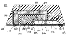
- An IC device is packaged in a BGA substrate 5 .
- Semiconductor device 100 is attached on an attachment area 10 .
- the semiconductor device 100 has a plurality of bonding pads 20 a , 25 a , 30 a , and 35 a .
- a lead frame with a plurality of bonding fingers 20 b , 25 b , 30 b , and 35 b surrounds the die attachment area 10 .
- Each of these respective bonding pads ( 20 a , 25 a , 30 a , and 35 a ) and bonding fingers ( 20 b , 25 b , 30 b , and 35 b ) will be connected to one another.
- bonding finger 25 b is a voltage (VDD) connection and bonding finger 30 b is a ground (GND) connection, and bonding finger 20 b is one signal (SIG) connection.
- VDD voltage
- GND ground
- SIG signal
- Another signal connection (SIG 2 ) bond finger 35 b is connected with a bond wire to bond pad 35 a.
- a layer of insulating material 15 applied to the substrate 5 A conductive strap region 25 c is defined between the VDD bond finger 25 b and bond pad 25 a . Another conductive strap region 30 c is defined between the GND bond finger 30 b and bond pad 30 a . An opening 20 c is defined between SIG bond finger 20 b and bond finger 20 a . Another opening 35 c is defined between bond finger 35 b and bond pad 35 a .
- the conductive strap regions may be defined with photolithography. It may be integrated into the solder mask. Molded plastic areas may define trenches containing the conductive straps. In a particular process, parylene may be selectively applied by painting or spraying.
- a bond wire 40 connects the bond pad 20 a to a bonding finger 20 b that connects to a signal pin 55 .
- the bond wire 40 is covered with a resilient insulation 45 .
- automatic bonding apparatus dispenses insulated bond wire.
- Bond wire may be gold, copper, or aluminum depending on the particular application.
- the bond wire may be insulated with parylene, epoxy, or a polycarbonate.
- a conductive strap 30 d has been defined in the conductive strap region 30 c and connects the bonding pad 30 a to the bonding finger 30 b that connects to a package ground pin.
- a conductive strap 25 d has been defined in the conductive strap region 25 c .
- the bonding pad 25 a is connected to the bonding finger 25 b that connects to a package ground pin.
- Bond pad 35 a is connected to bond finger 35 b with a non-insulated bond wire 50 . In this area, there is little chance of adjacent bond wires flexing and touching one another during encapsulation in a passivating envelope.
- the conductive material may be sputtered metal, electro-plated metal, a conductive plastic applied as a slurry subjected to a curing process, or plasma-deposited metal, etc.
- Some conductive materials include, but are not limited to, copper, gold, silver, aluminum, nickel, conductive polymer, etc. Additional conductive materials may also include plastics having conductive fillers of aluminum, copper, silver, nickel, and carbon nanotubes, etc.
- the semiconductor device 100 having been electrically connected to the package, is encapsulated in a passivating envelope 50 .
- FIGS. 1D and 1E depict in side view to regions of the packaged semiconductor device 100 of FIG. 1C .
- FIG. 1D shows the conductive strap 25 d surrounded by the insulating material 15 at 15 a .
- FIG. 1E depicts to insulated bond wire 40 and non-insulated bond wire 50 .
- the passivating envelope 50 encapsulates these bond wires 40 , 50 .
- the insulating material 15 prevents the conductive straps 25 d and 30 d and from shifting owing to forces sustained during encapsulation.
- the insulated bond wire 40 has additional insulation applied at the bond finger and bond bad 45 a so that the ends of the insulation 45 are sealed.
- the bond wire 40 is fully insulated.
- a conductive material can envelope the fully insulated bond wire.
- the conductive material is connected to a reference voltage, such as power and ground. Having the reference voltage closer to the fully insulated bond wire reduces the impedance of the bond wire with respect to that voltage reference.
- the embodiments mentioned thus far are applicable to a single layer of insulating material applied to the substrate and the conductive straps are situated on one level.
- the present invention may be applied in a substrate in which multiple levels of conductive straps and insulating layers may be used.
- a semiconductor device 200 is assembled according to an embodiment of the present invention.
- a substrate 205 has respective bond fingers 210 b , 215 b , 220 b , and 225 b for power (PWR), ground (GND), signal (SIG), and a second signal (SIG 2 ).
- PWR power
- GND ground
- SIG signal
- SIG 2 second signal
- These bond pads are electrically connected to corresponding bond fingers 210 b , 215 b , 220 b , and 225 b , upon which solder balls may be attached.
- SIG has bond wire 250 connecting its bond finger 220 b to bond pad 220 a on semiconductor device 200 .
- Bond wire 250 is surrounded with insulating material 255 .
- the bond wire 250 with insulating material 255 may be encapsulated in another insulating material 260 ; at the bond pad 222 a , the bond wire 250 with insulating material 255 may be encapsulated with another insulating material 265 .
- a conductive strap 215 connects the pad landing 215 b (GND) with bond pad 215 a .
- insulating material 270 may be applied.
- a subsequent conductive layer 210 c connects bond finger 210 b (PWR).
- the insulating material 270 prevents the short-circuiting of conductive strap 210 c with conductive strap 215 .
- an additional insulating layer 275 may be applied.
- bond wire 230 connects bond pad 225 a with bond finger 225 b at SIG 2 .
- the package as depicted in FIG. 1 may be used, however additional insulated dams are defined between the conductive straps. These dams reduce the probability that the conductive straps move and possibly short-circuit one another during encapsulation.
- a separate power bus and ground bus may be defined for an inner core and a power/ground bus for an outer ring of input/output pins. Often, these separate power/ground buses help improve device performance by isolating input/output switching transients from the IC device core.
- the present invention may be applied to a variety of packages using wire bonding to connect IC device die.
- the packages may include, but not limited to leadless chip carriers (LCC), ball grid arrays (BGA), etc.
- LCC leadless chip carriers
- BGA ball grid arrays
- FIG. 3 the user first selects a suitable package type 110 .
- the locations 120 of voltage reference pins i.e., the VDD and GND
- the locations 130 of the signal pins i.e., inputs and outputs
- Those signal pins in which impedance has to be controlled may be located closer to voltage reference pins.
- the location of the conductive straps that connect IC bond pads with their respective package bond fingers are defined 140 .
- a strap mask is generated so that insulating trenches and dams may be printed onto the package substrate. These trenches may be formed with resilient insulating materials. These insulating materials may include, but are not limited to, epoxy, thermoplastic, or silicone, etc.
- the strap mask pattern is applied through standard lithography techniques. A trench surrounding an IC bond pad and its corresponding bonding finger is created. The user applies a conductive material to fill the trenches 150 .
- the voltage references have a more robust electrical connection than that afforded by bonding wires, in that higher currents may pass through them.
- those pins using wire bonds are bonded 160 .
- bond wire covered with a resilient insulating material is used.
- additional insulation 170 may be added.
- the package undergoes encapsulation 180 in a suitable molding compound.
Abstract
Description
Claims (20)
Priority Applications (1)
| Application Number | Priority Date | Filing Date | Title |
|---|---|---|---|
| US12/294,211 US8203219B2 (en) | 2006-03-23 | 2007-03-23 | Electrically enhanced wirebond package |
Applications Claiming Priority (4)
| Application Number | Priority Date | Filing Date | Title |
|---|---|---|---|
| US78590806P | 2006-03-23 | 2006-03-23 | |
| IBPCT/IB2007/050997 | 2007-03-23 | ||
| PCT/IB2007/050997 WO2007107964A1 (en) | 2006-03-23 | 2007-03-23 | Electrically enhanced wirebond package |
| US12/294,211 US8203219B2 (en) | 2006-03-23 | 2007-03-23 | Electrically enhanced wirebond package |
Publications (2)
| Publication Number | Publication Date |
|---|---|
| US20090102067A1 US20090102067A1 (en) | 2009-04-23 |
| US8203219B2 true US8203219B2 (en) | 2012-06-19 |
Family
ID=38283993
Family Applications (1)
| Application Number | Title | Priority Date | Filing Date |
|---|---|---|---|
| US12/294,211 Active 2029-07-22 US8203219B2 (en) | 2006-03-23 | 2007-03-23 | Electrically enhanced wirebond package |
Country Status (5)
| Country | Link |
|---|---|
| US (1) | US8203219B2 (en) |
| EP (1) | EP2002478B1 (en) |
| JP (1) | JP5340912B2 (en) |
| CN (1) | CN101410974B (en) |
| WO (1) | WO2007107964A1 (en) |
Cited By (4)
| Publication number | Priority date | Publication date | Assignee | Title |
|---|---|---|---|---|
| US20150155243A1 (en) * | 2013-12-04 | 2015-06-04 | Taiwan Semiconductor Manufacturing Company, Ltd. | Warpage Control in Package-on-Package Structures |
| US20150235927A1 (en) * | 2014-02-19 | 2015-08-20 | Dsp Group Ltd. | Integrated circuit package |
| US20160172274A1 (en) * | 2014-12-16 | 2016-06-16 | Qualcomm Incorporated | System, apparatus, and method for semiconductor package grounds |
| US11508687B2 (en) | 2020-02-07 | 2022-11-22 | Samsung Electronics Co., Ltd. | Semiconductor package |
Families Citing this family (25)
| Publication number | Priority date | Publication date | Assignee | Title |
|---|---|---|---|---|
| JP2009016383A (en) * | 2007-06-29 | 2009-01-22 | Fujitsu Ltd | Packaged device, and method of manufacturing packaged device |
| US20090243051A1 (en) * | 2008-03-28 | 2009-10-01 | Micron Technology, Inc. | Integrated conductive shield for microelectronic device assemblies and associated methods |
| US8138587B2 (en) * | 2008-09-30 | 2012-03-20 | Infineon Technologies Ag | Device including two mounting surfaces |
| KR101013557B1 (en) * | 2008-11-06 | 2011-02-14 | 주식회사 하이닉스반도체 | Flexible semiconductor package and wire bonding apparatus for manufacturing the same |
| JP2010199547A (en) | 2009-01-30 | 2010-09-09 | Nichia Corp | Light emitting device and method of manufacturing same |
| KR100935854B1 (en) | 2009-09-22 | 2010-01-08 | 테세라 리써치 엘엘씨 | Microelectronic assembly with impedance controlled wirebond and reference wirebond |
| KR100950511B1 (en) | 2009-09-22 | 2010-03-30 | 테세라 리써치 엘엘씨 | Microelectronic assembly with impedance controlled wirebond and conductive reference element |
| JP5481277B2 (en) * | 2010-06-04 | 2014-04-23 | シャープ株式会社 | Light emitting device |
| US9136197B2 (en) | 2010-09-16 | 2015-09-15 | Tessera, Inc. | Impedence controlled packages with metal sheet or 2-layer RDL |
| US8853708B2 (en) | 2010-09-16 | 2014-10-07 | Tessera, Inc. | Stacked multi-die packages with impedance control |
| US8786083B2 (en) | 2010-09-16 | 2014-07-22 | Tessera, Inc. | Impedance controlled packages with metal sheet or 2-layer RDL |
| US8581377B2 (en) | 2010-09-16 | 2013-11-12 | Tessera, Inc. | TSOP with impedance control |
| US9035435B2 (en) * | 2012-11-14 | 2015-05-19 | Power Integrations, Inc. | Magnetically coupled galvanically isolated communication using lead frame |
| EP3017470B1 (en) * | 2013-07-03 | 2018-10-24 | Rosenberger Hochfrequenztechnik GmbH & Co. KG | Electronic device having a lead with selectively modified electrical properties and method of manufacturing the same |
| US9756726B2 (en) * | 2013-11-04 | 2017-09-05 | Infineon Technologies Ag | Electronic device and method of fabricating an electronic device |
| US9263420B2 (en) * | 2013-12-05 | 2016-02-16 | Freescale Semiconductor, Inc. | Devices and stacked microelectronic packages with package surface conductors and methods of their fabrication |
| CN103928452A (en) * | 2014-04-28 | 2014-07-16 | 张家港市大明玻璃制品有限公司 | Novel solar photoelectric glass |
| US10388607B2 (en) | 2014-12-17 | 2019-08-20 | Nxp Usa, Inc. | Microelectronic devices with multi-layer package surface conductors and methods of their fabrication |
| US9842831B2 (en) * | 2015-05-14 | 2017-12-12 | Mediatek Inc. | Semiconductor package and fabrication method thereof |
| US10685943B2 (en) | 2015-05-14 | 2020-06-16 | Mediatek Inc. | Semiconductor chip package with resilient conductive paste post and fabrication method thereof |
| US10224306B2 (en) | 2016-11-03 | 2019-03-05 | Stmicroelectronics (Grenoble 2) Sas | Method for forming an electrical connection between an electronic chip and a carrier substrate and electronic device |
| CN107833838B (en) * | 2017-11-22 | 2019-10-18 | 华进半导体封装先导技术研发中心有限公司 | A kind of the high reliability packaging structure and its manufacturing method of air-tightness device |
| IT201800004209A1 (en) * | 2018-04-05 | 2019-10-05 | SEMICONDUCTIVE POWER DEVICE WITH RELATIVE ENCAPSULATION AND CORRESPONDING MANUFACTURING PROCEDURE | |
| IT201900013743A1 (en) | 2019-08-01 | 2021-02-01 | St Microelectronics Srl | ENCAPSULATED ELECTRONIC POWER DEVICE, IN PARTICULAR BRIDGE CIRCUIT INCLUDING POWER TRANSISTORS, AND RELATED ASSEMBLY PROCEDURE |
| IT202000016840A1 (en) | 2020-07-10 | 2022-01-10 | St Microelectronics Srl | HIGH VOLTAGE ENCAPSULATED MOSFET DEVICE EQUIPPED WITH CONNECTION CLIP AND RELATED MANUFACTURING PROCEDURE |
Citations (22)
| Publication number | Priority date | Publication date | Assignee | Title |
|---|---|---|---|---|
| JPS57113234A (en) | 1980-12-29 | 1982-07-14 | Seiko Epson Corp | Structure of bonding wire |
| US4488674A (en) | 1981-10-12 | 1984-12-18 | Tokyo Shibaura Denki Kabushiki Kaisha | Bonding wire, semiconductor device having the same, and bonding method using the same |
| JPS62183544A (en) | 1986-02-07 | 1987-08-11 | Nec Corp | Resin molded semiconductor device |
| JPS63250832A (en) | 1987-04-08 | 1988-10-18 | Mitsubishi Electric Corp | Wire bonding |
| EP0418749A2 (en) | 1989-09-21 | 1991-03-27 | STMicroelectronics S.r.l. | Integrated device with improved connections between the pins and the semiconductor material chip |
| JPH0465840A (en) | 1990-07-06 | 1992-03-02 | Oki Electric Ind Co Ltd | Resin-sealed semiconductor device and its manufacture |
| US5170930A (en) | 1991-11-14 | 1992-12-15 | Microelectronics And Computer Technology Corporation | Liquid metal paste for thermal and electrical connections |
| JPH06216183A (en) | 1992-12-10 | 1994-08-05 | Internatl Business Mach Corp <Ibm> | Constituent of ic chip and its preparation |
| EP0786806A1 (en) | 1996-01-23 | 1997-07-30 | Montpellier Technologies | High I/O density package for high power wire-bonded IC chips and method for making the same |
| US5986885A (en) * | 1997-04-08 | 1999-11-16 | Integrated Device Technology, Inc. | Semiconductor package with internal heatsink and assembly method |
| US6023103A (en) * | 1994-11-15 | 2000-02-08 | Formfactor, Inc. | Chip-scale carrier for semiconductor devices including mounted spring contacts |
| US6046075A (en) | 1997-12-23 | 2000-04-04 | Vlsi Technology, Inc. | Oxide wire bond insulation in semiconductor assemblies |
| JP2002170842A (en) | 2000-11-20 | 2002-06-14 | Texas Instruments Inc | Semiconductor device bonded by wire with small coupling capacitance |
| US20020117330A1 (en) * | 1993-11-16 | 2002-08-29 | Formfactor, Inc. | Resilient contact structures formed and then attached to a substrate |
| US6534711B1 (en) * | 1998-04-14 | 2003-03-18 | The Goodyear Tire & Rubber Company | Encapsulation package and method of packaging an electronic circuit module |
| US20030089983A1 (en) | 2001-11-15 | 2003-05-15 | Siliconware Precision Industries Co., Ltd. | Ball grid array semiconductor package |
| US20040014309A1 (en) | 2002-07-17 | 2004-01-22 | Texas Instruments Incorporated | Multilayer laser trim interconnect method |
| US6727579B1 (en) * | 1994-11-16 | 2004-04-27 | Formfactor, Inc. | Electrical contact structures formed by configuring a flexible wire to have a springable shape and overcoating the wire with at least one layer of a resilient conductive material, methods of mounting the contact structures to electronic components, and applications for employing the contact structures |
| US20040119172A1 (en) | 2002-12-18 | 2004-06-24 | Downey Susan H. | Packaged IC using insulated wire |
| US20040124546A1 (en) * | 2002-12-29 | 2004-07-01 | Mukul Saran | Reliable integrated circuit and package |
| JP2005099301A (en) | 2003-09-24 | 2005-04-14 | Seiko Epson Corp | Packaged structure, electrooptical device, electronic equipment, and method for manufacturing packaged structure |
| US20060226534A1 (en) | 2005-03-18 | 2006-10-12 | Silicon Integrated Systems Corp. | Structure and assembly method of integrated circuit package |
Family Cites Families (3)
| Publication number | Priority date | Publication date | Assignee | Title |
|---|---|---|---|---|
| EP0924762A3 (en) * | 1997-12-22 | 2002-04-24 | Siemens Aktiengesellschaft | Interconnections in integrated circuit devices |
| JP2000058579A (en) * | 1998-08-04 | 2000-02-25 | Hitachi Ltd | Semiconductor device and its manufacture |
| US7685497B2 (en) | 2004-03-31 | 2010-03-23 | Nxp B.V. | Method and apparatus for efficient computation of check equations in periodical low density parity check (LDPC) codes |
-
2007
- 2007-03-23 JP JP2009501011A patent/JP5340912B2/en active Active
- 2007-03-23 WO PCT/IB2007/050997 patent/WO2007107964A1/en active Application Filing
- 2007-03-23 EP EP07735213.6A patent/EP2002478B1/en active Active
- 2007-03-23 CN CN2007800104244A patent/CN101410974B/en active Active
- 2007-03-23 US US12/294,211 patent/US8203219B2/en active Active
Patent Citations (23)
| Publication number | Priority date | Publication date | Assignee | Title |
|---|---|---|---|---|
| JPS57113234A (en) | 1980-12-29 | 1982-07-14 | Seiko Epson Corp | Structure of bonding wire |
| US4488674A (en) | 1981-10-12 | 1984-12-18 | Tokyo Shibaura Denki Kabushiki Kaisha | Bonding wire, semiconductor device having the same, and bonding method using the same |
| JPS62183544A (en) | 1986-02-07 | 1987-08-11 | Nec Corp | Resin molded semiconductor device |
| JPS63250832A (en) | 1987-04-08 | 1988-10-18 | Mitsubishi Electric Corp | Wire bonding |
| EP0418749A2 (en) | 1989-09-21 | 1991-03-27 | STMicroelectronics S.r.l. | Integrated device with improved connections between the pins and the semiconductor material chip |
| JPH0465840A (en) | 1990-07-06 | 1992-03-02 | Oki Electric Ind Co Ltd | Resin-sealed semiconductor device and its manufacture |
| US5170930A (en) | 1991-11-14 | 1992-12-15 | Microelectronics And Computer Technology Corporation | Liquid metal paste for thermal and electrical connections |
| JPH06216183A (en) | 1992-12-10 | 1994-08-05 | Internatl Business Mach Corp <Ibm> | Constituent of ic chip and its preparation |
| US5622898A (en) | 1992-12-10 | 1997-04-22 | International Business Machines Corporation | Process of making an integrated circuit chip composite including parylene coated wire |
| US20020117330A1 (en) * | 1993-11-16 | 2002-08-29 | Formfactor, Inc. | Resilient contact structures formed and then attached to a substrate |
| US6023103A (en) * | 1994-11-15 | 2000-02-08 | Formfactor, Inc. | Chip-scale carrier for semiconductor devices including mounted spring contacts |
| US6727579B1 (en) * | 1994-11-16 | 2004-04-27 | Formfactor, Inc. | Electrical contact structures formed by configuring a flexible wire to have a springable shape and overcoating the wire with at least one layer of a resilient conductive material, methods of mounting the contact structures to electronic components, and applications for employing the contact structures |
| EP0786806A1 (en) | 1996-01-23 | 1997-07-30 | Montpellier Technologies | High I/O density package for high power wire-bonded IC chips and method for making the same |
| US5986885A (en) * | 1997-04-08 | 1999-11-16 | Integrated Device Technology, Inc. | Semiconductor package with internal heatsink and assembly method |
| US6046075A (en) | 1997-12-23 | 2000-04-04 | Vlsi Technology, Inc. | Oxide wire bond insulation in semiconductor assemblies |
| US6534711B1 (en) * | 1998-04-14 | 2003-03-18 | The Goodyear Tire & Rubber Company | Encapsulation package and method of packaging an electronic circuit module |
| JP2002170842A (en) | 2000-11-20 | 2002-06-14 | Texas Instruments Inc | Semiconductor device bonded by wire with small coupling capacitance |
| US20030089983A1 (en) | 2001-11-15 | 2003-05-15 | Siliconware Precision Industries Co., Ltd. | Ball grid array semiconductor package |
| US20040014309A1 (en) | 2002-07-17 | 2004-01-22 | Texas Instruments Incorporated | Multilayer laser trim interconnect method |
| US20040119172A1 (en) | 2002-12-18 | 2004-06-24 | Downey Susan H. | Packaged IC using insulated wire |
| US20040124546A1 (en) * | 2002-12-29 | 2004-07-01 | Mukul Saran | Reliable integrated circuit and package |
| JP2005099301A (en) | 2003-09-24 | 2005-04-14 | Seiko Epson Corp | Packaged structure, electrooptical device, electronic equipment, and method for manufacturing packaged structure |
| US20060226534A1 (en) | 2005-03-18 | 2006-10-12 | Silicon Integrated Systems Corp. | Structure and assembly method of integrated circuit package |
Non-Patent Citations (1)
| Title |
|---|
| Japanese Patent Office, Office Action dated Aug. 30, 2011, Application No. 2009-501011, 2 pages. |
Cited By (9)
| Publication number | Priority date | Publication date | Assignee | Title |
|---|---|---|---|---|
| US20150155243A1 (en) * | 2013-12-04 | 2015-06-04 | Taiwan Semiconductor Manufacturing Company, Ltd. | Warpage Control in Package-on-Package Structures |
| US9559064B2 (en) * | 2013-12-04 | 2017-01-31 | Taiwan Semiconductor Manufacturing Company, Ltd. | Warpage control in package-on-package structures |
| US9941221B2 (en) | 2013-12-04 | 2018-04-10 | Taiwan Semiconductor Manufacturing Company, Ltd. | Warpage control in package-on-package structures |
| US10170434B2 (en) | 2013-12-04 | 2019-01-01 | Taiwan Semiconductor Manufacturing Company, Ltd. | Warpage control in package-on-package structures |
| US10535616B2 (en) | 2013-12-04 | 2020-01-14 | Taiwan Semiconductor Manufacturing Company, Ltd. | Warpage control in package-on-package structures |
| US20150235927A1 (en) * | 2014-02-19 | 2015-08-20 | Dsp Group Ltd. | Integrated circuit package |
| US9514957B2 (en) * | 2014-02-19 | 2016-12-06 | Dsp Group Ltd. | Integrated circuit package |
| US20160172274A1 (en) * | 2014-12-16 | 2016-06-16 | Qualcomm Incorporated | System, apparatus, and method for semiconductor package grounds |
| US11508687B2 (en) | 2020-02-07 | 2022-11-22 | Samsung Electronics Co., Ltd. | Semiconductor package |
Also Published As
| Publication number | Publication date |
|---|---|
| JP5340912B2 (en) | 2013-11-13 |
| EP2002478B1 (en) | 2016-09-07 |
| US20090102067A1 (en) | 2009-04-23 |
| EP2002478A1 (en) | 2008-12-17 |
| CN101410974B (en) | 2013-02-20 |
| CN101410974A (en) | 2009-04-15 |
| WO2007107964A1 (en) | 2007-09-27 |
| JP2009530842A (en) | 2009-08-27 |
Similar Documents
| Publication | Publication Date | Title |
|---|---|---|
| US8203219B2 (en) | Electrically enhanced wirebond package | |
| US8310064B2 (en) | Semiconductor devices including voltage switchable materials for over-voltage protection | |
| US7154186B2 (en) | Multi-flip chip on lead frame on over molded IC package and method of assembly | |
| US6552417B2 (en) | Molded plastic package with heat sink and enhanced electrical performance | |
| US7378298B2 (en) | Method of making stacked die package | |
| US8129226B2 (en) | Power lead-on-chip ball grid array package | |
| US7825526B2 (en) | Fine-pitch routing in a lead frame based system-in-package (SIP) device | |
| US20060094161A1 (en) | Thermal enhance package and manufacturing method thereof | |
| US20090057915A1 (en) | Semiconductor device | |
| US10582617B2 (en) | Method of fabricating a circuit module | |
| EP1911080B1 (en) | Flip-chip package with air cavity | |
| US20090302483A1 (en) | Stacked die package | |
| KR20060126645A (en) | Land grid array packaged device and method of forming same | |
| US20060125079A1 (en) | High density package interconnect wire bond strip line and method therefor | |
| CN107342276B (en) | Semiconductor device and corresponding method | |
| US20070281393A1 (en) | Method of forming a trace embedded package | |
| US9721928B1 (en) | Integrated circuit package having two substrates | |
| WO2008114094A1 (en) | Thin profile packaging with exposed die attach adhesive | |
| US20080315432A1 (en) | Electrical Shielding in Stacked Dies by Using Conductive Die Dttach Adhesive | |
| US11869837B2 (en) | Semiconductor device packaging extendable lead and method therefor | |
| US20240014123A1 (en) | Semiconductor device with lead-on-chip interconnect and method therefor | |
| US20220102258A1 (en) | Semiconductor device and corresponding method of manufacturing semiconductor devices |
Legal Events
| Date | Code | Title | Description |
|---|---|---|---|
| AS | Assignment |
Owner name: NXP, B.V., NETHERLANDS Free format text: ASSIGNMENT OF ASSIGNORS INTEREST;ASSIGNOR:WYLAND, CHRIS;REEL/FRAME:021574/0102 Effective date: 20080322 |
|
| AS | Assignment |
Owner name: TAIWAN SEMICONDUCTOR MANUFACTURING COMPANY, LTD., Free format text: ASSIGNMENT OF ASSIGNORS INTEREST;ASSIGNOR:NXP B.V.;REEL/FRAME:022266/0047 Effective date: 20090217 Owner name: TAIWAN SEMICONDUCTOR MANUFACTURING COMPANY, LTD.,T Free format text: ASSIGNMENT OF ASSIGNORS INTEREST;ASSIGNOR:NXP B.V.;REEL/FRAME:022266/0047 Effective date: 20090217 |
|
| STCF | Information on status: patent grant |
Free format text: PATENTED CASE |
|
| FPAY | Fee payment |
Year of fee payment: 4 |
|
| AS | Assignment |
Owner name: MORGAN STANLEY SENIOR FUNDING, INC., MARYLAND Free format text: SECURITY AGREEMENT SUPPLEMENT;ASSIGNOR:NXP B.V.;REEL/FRAME:038017/0058 Effective date: 20160218 |
|
| AS | Assignment |
Owner name: MORGAN STANLEY SENIOR FUNDING, INC., MARYLAND Free format text: CORRECTIVE ASSIGNMENT TO CORRECT THE REMOVE APPLICATION 12092129 PREVIOUSLY RECORDED ON REEL 038017 FRAME 0058. ASSIGNOR(S) HEREBY CONFIRMS THE SECURITY AGREEMENT SUPPLEMENT;ASSIGNOR:NXP B.V.;REEL/FRAME:039361/0212 Effective date: 20160218 |
|
| AS | Assignment |
Owner name: NXP B.V., NETHERLANDS Free format text: PATENT RELEASE;ASSIGNOR:MORGAN STANLEY SENIOR FUNDING, INC.;REEL/FRAME:039707/0471 Effective date: 20160805 |
|
| AS | Assignment |
Owner name: MORGAN STANLEY SENIOR FUNDING, INC., MARYLAND Free format text: CORRECTIVE ASSIGNMENT TO CORRECT THE REMOVE APPLICATION 12681366 PREVIOUSLY RECORDED ON REEL 039361 FRAME 0212. ASSIGNOR(S) HEREBY CONFIRMS THE SECURITY AGREEMENT SUPPLEMENT;ASSIGNOR:NXP B.V.;REEL/FRAME:042762/0145 Effective date: 20160218 Owner name: MORGAN STANLEY SENIOR FUNDING, INC., MARYLAND Free format text: CORRECTIVE ASSIGNMENT TO CORRECT THE REMOVE APPLICATION 12681366 PREVIOUSLY RECORDED ON REEL 038017 FRAME 0058. ASSIGNOR(S) HEREBY CONFIRMS THE SECURITY AGREEMENT SUPPLEMENT;ASSIGNOR:NXP B.V.;REEL/FRAME:042985/0001 Effective date: 20160218 |
|
| AS | Assignment |
Owner name: NXP B.V., NETHERLANDS Free format text: RELEASE BY SECURED PARTY;ASSIGNOR:MORGAN STANLEY SENIOR FUNDING, INC.;REEL/FRAME:050745/0001 Effective date: 20190903 |
|
| AS | Assignment |
Owner name: MORGAN STANLEY SENIOR FUNDING, INC., MARYLAND Free format text: CORRECTIVE ASSIGNMENT TO CORRECT THE REMOVE APPLICATION 12298143 PREVIOUSLY RECORDED ON REEL 042762 FRAME 0145. ASSIGNOR(S) HEREBY CONFIRMS THE SECURITY AGREEMENT SUPPLEMENT;ASSIGNOR:NXP B.V.;REEL/FRAME:051145/0184 Effective date: 20160218 Owner name: MORGAN STANLEY SENIOR FUNDING, INC., MARYLAND Free format text: CORRECTIVE ASSIGNMENT TO CORRECT THE REMOVE APPLICATION 12298143 PREVIOUSLY RECORDED ON REEL 039361 FRAME 0212. ASSIGNOR(S) HEREBY CONFIRMS THE SECURITY AGREEMENT SUPPLEMENT;ASSIGNOR:NXP B.V.;REEL/FRAME:051029/0387 Effective date: 20160218 Owner name: MORGAN STANLEY SENIOR FUNDING, INC., MARYLAND Free format text: CORRECTIVE ASSIGNMENT TO CORRECT THE REMOVE APPLICATION 12298143 PREVIOUSLY RECORDED ON REEL 042985 FRAME 0001. ASSIGNOR(S) HEREBY CONFIRMS THE SECURITY AGREEMENT SUPPLEMENT;ASSIGNOR:NXP B.V.;REEL/FRAME:051029/0001 Effective date: 20160218 Owner name: MORGAN STANLEY SENIOR FUNDING, INC., MARYLAND Free format text: CORRECTIVE ASSIGNMENT TO CORRECT THE REMOVE APPLICATION 12298143 PREVIOUSLY RECORDED ON REEL 038017 FRAME 0058. ASSIGNOR(S) HEREBY CONFIRMS THE SECURITY AGREEMENT SUPPLEMENT;ASSIGNOR:NXP B.V.;REEL/FRAME:051030/0001 Effective date: 20160218 Owner name: MORGAN STANLEY SENIOR FUNDING, INC., MARYLAND Free format text: CORRECTIVE ASSIGNMENT TO CORRECT THE REMOVE APPLICATION12298143 PREVIOUSLY RECORDED ON REEL 042985 FRAME 0001. ASSIGNOR(S) HEREBY CONFIRMS THE SECURITY AGREEMENT SUPPLEMENT;ASSIGNOR:NXP B.V.;REEL/FRAME:051029/0001 Effective date: 20160218 Owner name: MORGAN STANLEY SENIOR FUNDING, INC., MARYLAND Free format text: CORRECTIVE ASSIGNMENT TO CORRECT THE REMOVE APPLICATION12298143 PREVIOUSLY RECORDED ON REEL 039361 FRAME 0212. ASSIGNOR(S) HEREBY CONFIRMS THE SECURITY AGREEMENT SUPPLEMENT;ASSIGNOR:NXP B.V.;REEL/FRAME:051029/0387 Effective date: 20160218 Owner name: MORGAN STANLEY SENIOR FUNDING, INC., MARYLAND Free format text: CORRECTIVE ASSIGNMENT TO CORRECT THE REMOVE APPLICATION12298143 PREVIOUSLY RECORDED ON REEL 042762 FRAME 0145. ASSIGNOR(S) HEREBY CONFIRMS THE SECURITY AGREEMENT SUPPLEMENT;ASSIGNOR:NXP B.V.;REEL/FRAME:051145/0184 Effective date: 20160218 |
|
| MAFP | Maintenance fee payment |
Free format text: PAYMENT OF MAINTENANCE FEE, 8TH YEAR, LARGE ENTITY (ORIGINAL EVENT CODE: M1552); ENTITY STATUS OF PATENT OWNER: LARGE ENTITY Year of fee payment: 8 |
|
| MAFP | Maintenance fee payment |
Free format text: PAYMENT OF MAINTENANCE FEE, 12TH YEAR, LARGE ENTITY (ORIGINAL EVENT CODE: M1553); ENTITY STATUS OF PATENT OWNER: LARGE ENTITY Year of fee payment: 12 |