US8215946B2 - Imprint lithography system and method - Google Patents
Imprint lithography system and method Download PDFInfo
- Publication number
- US8215946B2 US8215946B2 US12/582,091 US58209109A US8215946B2 US 8215946 B2 US8215946 B2 US 8215946B2 US 58209109 A US58209109 A US 58209109A US 8215946 B2 US8215946 B2 US 8215946B2
- Authority
- US
- United States
- Prior art keywords
- substrate
- template
- chuck
- height
- mold
- Prior art date
- Legal status (The legal status is an assumption and is not a legal conclusion. Google has not performed a legal analysis and makes no representation as to the accuracy of the status listed.)
- Expired - Fee Related
Links
Images


Classifications
-
- G—PHYSICS
- G03—PHOTOGRAPHY; CINEMATOGRAPHY; ANALOGOUS TECHNIQUES USING WAVES OTHER THAN OPTICAL WAVES; ELECTROGRAPHY; HOLOGRAPHY
- G03F—PHOTOMECHANICAL PRODUCTION OF TEXTURED OR PATTERNED SURFACES, e.g. FOR PRINTING, FOR PROCESSING OF SEMICONDUCTOR DEVICES; MATERIALS THEREFOR; ORIGINALS THEREFOR; APPARATUS SPECIALLY ADAPTED THEREFOR
- G03F7/00—Photomechanical, e.g. photolithographic, production of textured or patterned surfaces, e.g. printing surfaces; Materials therefor, e.g. comprising photoresists; Apparatus specially adapted therefor
- G03F7/0002—Lithographic processes using patterning methods other than those involving the exposure to radiation, e.g. by stamping
-
- B—PERFORMING OPERATIONS; TRANSPORTING
- B82—NANOTECHNOLOGY
- B82Y—SPECIFIC USES OR APPLICATIONS OF NANOSTRUCTURES; MEASUREMENT OR ANALYSIS OF NANOSTRUCTURES; MANUFACTURE OR TREATMENT OF NANOSTRUCTURES
- B82Y10/00—Nanotechnology for information processing, storage or transmission, e.g. quantum computing or single electron logic
-
- B—PERFORMING OPERATIONS; TRANSPORTING
- B82—NANOTECHNOLOGY
- B82Y—SPECIFIC USES OR APPLICATIONS OF NANOSTRUCTURES; MEASUREMENT OR ANALYSIS OF NANOSTRUCTURES; MANUFACTURE OR TREATMENT OF NANOSTRUCTURES
- B82Y40/00—Manufacture or treatment of nanostructures
Definitions
- Nano-fabrication includes the fabrication of very small structures that have features on the order of 100 nanometers or smaller.
- One application in which nano-fabrication has had a sizeable impact is in the processing of integrated circuits.
- the semiconductor processing industry continues to strive for larger production yields, while increasing the circuits per unit area formed on a substrate; therefore, nano-fabrication becomes increasingly important.
- Nano-fabrication provides greater process control while allowing continued reduction of the minimum feature dimensions of the structures formed.
- Other areas of development in which nano-fabrication has been employed include biotechnology, optical technology, mechanical systems, and the like.
- imprint lithography An exemplary nano-fabrication technique in use today is commonly referred to as imprint lithography.
- Exemplary imprint lithography processes are described in detail in numerous publications, such as U.S. Patent Publication No. 2004/0065976, U.S. Patent Publication No. 2004/0065252, and U.S. Pat. No. 6,936,194, all of which are hereby incorporated by reference.
- An imprint lithography technique disclosed in each of the aforementioned U.S. patent publications and patent includes formation of a relief pattern in a polymerizable layer and transferring a pattern corresponding to the relief pattern into an underlying substrate.
- the substrate may be coupled to a motion stage to obtain a desired positioning to facilitate the patterning process. Additionally, the substrate may be coupled to a substrate chuck.
- the patterning process uses a template spaced apart from the substrate and a formable liquid applied between the template and the substrate.
- the formable liquid is solidified to form a rigid layer that has a pattern conforming to a shape of the surface of the template that contacts the formable liquid.
- the template is separated from the rigid layer such that the template and the substrate are spaced apart.
- the substrate and the solidified layer are then subjected to additional processes to transfer a relief image into the substrate that corresponds to the pattern in the solidified layer.
- FIG. 1 is a simplified side view of a lithographic system having a patterning device spaced-apart from a substrate, the patterning device comprising a template and a mold;
- FIG. 2 is a top down view of the substrate shown in FIG. 1 , the substrate having an inner, middle, and outer radius;
- FIG. 3 is a side view of the substrate shown in FIG. 1 coupled to a substrate chuck;
- FIG. 4 is a bottom-up plan view of the substrate chuck shown in FIG. 3
- FIG. 5 is a top down view of the template shown in FIG. 1 , having a mold coupled thereto;
- FIG. 6 is a side view of the template shown in FIG. 1 coupled to a template chuck;
- FIG. 7 is a bottom-up plan view of the template chuck shown in FIG. 6 ;
- FIG. 8 is a top down view showing an array of droplets of imprinting material positioned upon a region of the substrate shown in FIG. 1 ;
- FIG. 9 is a simplified side view of the substrate shown in FIG. 1 , having a patterned layer positioned thereon;
- FIG. 10 is a flow diagram showing a method of patterning the substrate shown in FIG. 1 , in a first embodiment
- FIG. 11 is a side view of the patterning device shown in FIG. 1 having an altered shape
- FIG. 12 is a side view of the patterning device shown in FIG. 11 , in contact with a portion of the droplets of imprinting material shown in FIG. 8 ;
- FIGS. 13-15 are top down views showing the compression of the droplets shown in FIG. 8 , employing the altered shape of the template shown in FIG. 12 ;
- FIG. 16 is a flow diagram showing a method of patterning a region of the substrate shown in FIG. 1 , in a second embodiment
- FIG. 17 is a side view of the substrate shown in FIG. 1 having an altered shape
- FIG. 18 is a side view of a pin exerting a force on the patterning device shown in FIG. 1 , to alter a shape thereof;
- FIG. 19 is a side view of the system shown in FIG. 1 , with a gas being introduced between the patterning device and the mold.
- FIG. 20 is a simplified side view of an exemplary substrate chuck providing substrate in a single wave formation.
- FIGS. 21A-21C are simplified side view of an exemplary substrate chuck providing substrate in multiple exemplary formations.
- FIGS. 22A and 22B are simplified side views of an exemplary substrate chuck having exemplary outer lands.
- FIG. 23 is a simplified side view of an exemplary template chuck and an exemplary, substrate chuck providing an imprint lithography template and a substrate in single wave formations.
- FIG. 24A-24D are simplified side view of another exemplary template chuck and an exemplary substrate chuck providing an imprint lithography template in a double wave formation and a substrate in a single wave formation.
- FIG. 25 is a top down view of a substrate subjected to forces.
- FIG. 26 is a simplified side view of an exemplary holding system in a first position, the first position constraining a substrate during separation of a template from the substrate.
- FIG. 27 is a simplified side view of the holding system illustrated in FIG. 26 in a second position, the second position distancing the holding system from the substrate.
- FIG. 28 illustrates a flow chart of an exemplary method for constraining a substrate during separation of a template from the substrate.
- Substrate 12 may have circular shape; however, in a further embodiment, substrate 12 may have any geometric shape.
- substrate 12 may have a disk shape having an inner radius r 1 and outer radius r 2 , with radius r 2 being greater than radius r 1 .
- inner radius r 1 and outer radius r 2 is defined between inner radius r 1 and outer radius r 2 .
- middle radius r 3 is defined between inner radius r 1 and outer radius r 2 .
- substrate 12 may be coupled to a substrate chuck 14 .
- substrate chuck 14 is a vacuum chuck, however, substrate chuck 14 may be any chuck including, but not limited to, vacuum, pin-type, groove-type, or electromagnetic, as described in U.S. Pat. No. 6,873,087 entitled “High-Precision Orientation Alignment and Gap Control Stages for Imprint Lithography Processes,” which is incorporated herein by reference.
- Substrate 12 and substrate chuck 14 may be supported upon a stage 16 . Further, substrate 12 , substrate chuck 14 , and stage 16 may be positioned on a base (not shown).
- Stage 16 may provide motion about a first and a second axis, with the first and the second axis being orthogonal to one another, i.e., the x and y axes.
- substrate chuck 14 includes first 18 and second 20 opposed sides.
- a side, or edge, surface 22 extends between first side 18 and second side 20 .
- First side 18 includes a first recess 20 , a second recess 22 , and a third recess 24 , defining first 26 , second 28 , third 30 , and fourth 32 spaced-apart support regions.
- First support region 26 cinctures second 28 , third 30 , and fourth 32 support regions and first 20 , second 22 , and third 24 recesses.
- Second support region 28 cinctures third 30 and fourth 32 support regions and second 22 and third 24 recesses.
- Third support region 30 cinctures fourth support region 32 and third recess 24 .
- Third recess 24 cinctures fourth support region 32 .
- first 26 , second 28 , third 30 , and fourth 32 support regions may be formed from a compliant material.
- First 26 , second 28 , third 30 , and fourth 32 support regions may have a circular shape; however, in a further embodiment, first 26 , second 28 , third 30 , and fourth 32 may comprise any geometric shape desired.
- substrate chuck 12 may comprise any number of throughways.
- Throughway 34 places first and third recesses 20 and 24 in fluid communication with side surface 18 , however, in a further embodiment, it should be understood that throughway 34 may place first and third recesses 20 and 24 in fluid communication with any surface of substrate chuck 14 .
- Throughway 36 places second recess 22 in fluid communication with side surface 18 , however, in a further embodiment, it should be understood that throughway 36 may place second recess 22 in fluid communication with any surface of substrate chuck 14 .
- throughway 34 facilitates placing first 20 and third 24 recesses and throughway 36 facilitates placing second recesses 22 in fluid communication with a pressure control system, such as a pump system 38 .
- Pump system 38 may include one or more pumps to control the pressure proximate to first 20 , second 22 , and third 24 recesses. To that end, when substrate 12 is coupled to substrate chuck 14 , substrate 12 rests against first 26 , second 28 , third 30 , and fourth 32 support regions, covering first 20 , second 22 , and third 24 recesses. First recess 20 and a portion 40 a of substrate 12 in superimposition therewith define a first chamber 42 . Second recess 22 and a portion 40 b of substrate 12 in superimposition therewith define a second chamber 44 . Third recesses 24 and a portion 40 c of substrate 12 in superimposition therewith define a third chamber 46 . Pump system 38 operates to control a pressure in first 42 , second 44 , and third 46 chambers.
- Patterning device 48 spaced-apart from substrate 12 is a patterning device 48 .
- Patterning device 48 comprises a template 50 having a mesa 52 extending therefrom towards substrate 12 with a patterning surface 54 thereon.
- mesa 52 may be referred to as a mold 52 .
- template 50 may be substantially absent of mold 52 .
- Template 50 and/or mold 52 may be formed from such materials including but not limited to, fused-silica, quartz, silicon, organic polymers, siloxane polymers, borosilicate glass, fluorocarbon polymers, metal, and hardened sapphire.
- patterning surface 54 comprises features defined by a plurality of spaced-apart recesses 56 and protrusions 58 .
- patterning surface 54 may be substantially smooth and/or planar. Patterning surface 54 may define an original pattern that forms the basis of a pattern to be formed on substrate 12 .
- template 50 may be coupled to a template chuck 60 , template chuck 60 being any chuck including, but not limited to, vacuum, pin-type, groove-type, or electromagnetic, as described in U.S. Pat. No. 6,873,087 entitled “High-Precision Orientation Alignment and Gap Control Stages for Imprint Lithography Processes”.
- Template chuck 60 includes first 62 and second 64 opposed sides. A side, or edge, surface 66 extends between first side 62 and second side 64 .
- First side 62 includes a first recess 68 , a second recess 70 , and a third recess 72 , defining first 74 , second 76 , and third 78 spaced-apart support regions.
- First support region 74 cinctures second 70 and third 72 support regions and first 68 , second 70 , and third 72 recesses.
- Second support region 76 cinctures third support region 78 and second 70 and third 72 recesses.
- Third support region 78 cinctures third recess 72 .
- first 74 , second 76 , and third 78 support regions may be formed from a compliant material.
- First 74 , second 76 , and third 78 support regions may have a circular shape; however, in a further embodiment, first 74 , second 76 , and third 78 support regions may have any geometric shape desired.
- template chuck 60 may comprise any number of throughways.
- Throughway 80 places first and third recesses 68 and 72 in fluid communication with second side 64 , however, in a further embodiment, it should be understood that throughway 80 may place first and third recesses 68 and 72 in fluid communication with any surface of template chuck 60 .
- Throughway 82 places second recess 70 in fluid communication with second side 64 , however, in a further embodiment, it should be understood that throughway 80 may place second recess 70 in fluid communication with any surface of template chuck 60 .
- throughway 80 facilitates placing first 68 and third 72 recesses and throughway 82 facilitates placing second recesses 70 in fluid communication with a pressure control system, such as a pump system 84 .
- Pump system 84 may include one or more pumps to control the pressure proximate to first 68 , second 70 , and third 72 recesses. To that end, when template 50 is coupled to template chuck 60 , template 50 rests against first 74 , second 76 , and third 78 support regions, covering first 68 , second 70 , and third 72 recesses. First recess 68 and a portion 86 a of template 50 in superimposition therewith define a first chamber 88 . Second recess 70 and a portion 86 b of template 50 in superimposition therewith define a second chamber 92 . Third recess 72 and a portion 86 c of substrate 12 in superimposition therewith define a third chamber 96 . Pump system 84 operates to control a pressure in first 88 , second 92 , and third 96 chambers. Further, template chuck 60 may be coupled to an imprint head 97 to facilitate movement of patterning device 48 .
- system 10 further comprises a fluid dispense system 98 .
- Fluid dispense system 98 may be in fluid communication with substrate 12 so as to deposit polymerizable material 100 thereon.
- Fluid dispense system 98 may comprise a plurality of dispensing units therein.
- polymerizable material 100 may be deposited using any known technique, e.g., drop dispense, spin-coating, dip coating, chemical vapor deposition (CVD), physical vapor deposition (PVD), thin film deposition, thick film deposition, and the like.
- CVD chemical vapor deposition
- PVD physical vapor deposition
- thin film deposition thick film deposition
- thick film deposition thick film deposition
- polymerizable material 100 may fill the volume after the desired volume has been obtained. As shown in FIG. 8 , polymerizable material 100 may be deposited upon substrate 12 as a plurality of spaced-apart droplets 102 , defining a matrix array 104 . In an example, each droplet of droplets 102 may have a unit volume of approximately 1-10 pico-liters. Droplets 102 may be arranged in any two-dimensional arrangement on substrate 12 .
- system 10 further comprises a source 106 of energy 108 coupled to direct energy 108 along a path 110 .
- Imprint head 97 and stage 16 are configured to arrange mold 52 and substrate 12 , respectively, to be in superimposition and disposed in path 110 . Either imprint head 97 , stage 16 , or both vary a distance between mold 52 and substrate 12 to define a desired volume therebetween that is filled by polymerizable material 100 .
- source 106 produces energy 108 , e.g., broadband ultraviolet radiation that causes polymerizable material 100 to solidify and/or cross-link conforming to the shape of a surface 112 of substrate 12 and patterning surface 54 , defining a patterned layer 114 on substrate 12 .
- Patterned layer 114 may comprise a residual layer 116 and a plurality of features shown as protrusions 118 and recessions 120 . Control of this process is regulated by a processor 122 that is in data communication with stage 16 , pump systems 38 and 84 , imprint head 97 , fluid dispense system 98 , and source 106 , operating on a computer readable program stored in a memory 124 .
- system 10 further includes a pin 126 coupled to stage 16 .
- Pin 126 may translate about a third axis orthogonal to the first and second axis, i.e., along the z axis. As a result, pin 126 may contact mold 52 to alter a shape thereof, described further below.
- Pin 126 may be any force or displacement actuator known in the art including, inter alia, pneumatic, piezoelectric, magnetostrictive, linear, and voice coils.
- pin 126 may be a high resolution pressure regulator and clean series air piston, with a center pin thereof comprising a vacuum source that may evacuate an atmosphere between an interface of patterning device 48 and substrate 12 .
- a distance between mold 52 and substrate 12 is varied such that a desired volume is defined therebetween that is filled by polymerizable material 100 . Furthermore, after solidification, polymerizable material 100 conforms to the shape of surface 112 of substrate 12 and patterning surface 54 , defining patterned layer 114 on substrate 12 . To that end, in a volume 128 defined between droplets 102 of matrix array 104 , there are gases present, and droplets 102 in matrix array 104 are spread over substrate 12 so as to avoid, if not prevent, trapping of gases and/or gas pockets between substrate 12 and mold 52 and within patterned layer 114 .
- the gases and/or gas pockets may be such gases including, but not limited to air, nitrogen, carbon dioxide, and helium.
- Gas and/or gas pockets between substrate 12 and mold 52 and within patterned layer 114 may result in, inter alia, pattern distortion of features formed in patterned layer 114 , low fidelity of features formed in patterned layer 114 , and a non-uniform thickness of residual layer 116 across patterned layer 114 , all of which are undesirable.
- a method and a system of minimizing, if not preventing, trapping of gas and/or gas pockets between substrate 12 and mold 52 and within patterned layer 114 are described below.
- polymerizable material 100 may be positioned on substrate 12 by drop dispense, spin-coating, dip coating, chemical vapor deposition (CVD), physical vapor deposition (PVD), thin film deposition, thick film deposition, and the like.
- polymerizable material 100 may be positioned on mold 52 .
- a shape of patterning device 48 may be altered. More specifically, a shape of patterning device 48 may be altered such that a distance d 1 defined between mold 52 and substrate 12 at middle radius r 3 of substrate 12 , shown in FIG. 2 , is less than a distance defined between mold 52 and substrate 12 at remaining portions of mold 52 . In an example, distance d 1 is less than a distance d 2 , distance d 2 being defined at an edge of mold 52 . In a further embodiment, the distance d 1 may be defined at any desired location of mold 52 .
- the shape of patterning device 48 may be altered by controlling a pressure within first and third chambers 68 and 72 .
- pump system 84 operates to control the pressure in first and third chambers 68 and 72 .
- pump system 84 may create a vacuum within first and third chambers 68 and 72 via throughway 80 such that portions 86 a and 86 c of template 50 may bow away from substrate 12 and bow towards template chuck 60 .
- portion 86 b of template 50 bows toward substrate 12 and away from template chuck 60 .
- either imprint head 97 shown in FIG. 1 , stage 16 , or both, may vary distance d 1 , shown in FIG. 11 , such that a portion of mold 52 contacts a sub-portion of droplets 102 .
- a portion of mold 52 in superimposition with middle radius r 3 of substrate 12 shown in FIG. 2 , contacts a sub-portion of droplets 102 prior to the remaining portions of mold 52 contacting the remaining droplets of droplets 102 .
- any portion of mold 52 may contact droplets 102 prior to remaining portions of mold 52 .
- mold 52 contacts all of droplets 102 in superimposition with middle radius r 3 of substrate 12 , shown in FIG. 2 , substantially concurrently.
- This causes droplets 102 to spread and to produce a contiguous liquid sheet 130 of polymerizable material 100 .
- Edge 132 of liquid sheet 130 defines a liquid-gas interface 134 that functions to push gases in volume 128 toward edge 136 of substrate 12 .
- Volume 128 between droplets 102 define gas passages through which gas may be pushed to edge 136 .
- liquid-gas interface 134 in conjunction with the gas passages reduces, if not prevents, trapping of gases in liquid sheet 130 .
- the shape of patterning device 48 may be altered such that the desired volume defined between mold 52 and substrate 12 may be filled by polymerizable material 100 , as described above with respect to FIG. 1 . More specifically, the shape of patterning device 48 may be altered by the combination of controlling the pressure within first and third chambers 88 and 96 and a force exerted by imprint head 97 , shown in FIG. 1 , and/or stage 16 upon patterning device 48 as a result of contact been polymerizable material 100 and mold 52 . More specifically, as mentioned above, pump system 84 operates to control the pressure in first and third chambers 88 and 96 .
- pump system 84 decreases a magnitude of the vacuum created within first and third chambers 88 and 96 via throughway 80 such that polymerizable material 100 associated with subsequent subsets of droplets 100 surrounding middle radius r 3 of substrate 12 shown in FIG. 2 , spread to become included in contiguous fluid sheet 130 , as shown in FIG. 14 .
- the shape of patterning device 48 continues to be altered such that mold 52 subsequently comes into contact with the remaining droplets 102 so that polymerizable material 100 associated therewith spreads to become included in contiguous sheet 130 , as shown in FIG. 15 .
- interface 134 has moved towards edge 136 so that there is an unimpeded path for the gases in the remaining volume 128 , shown in FIG. 8 , to travel thereto.
- a pressure within second chamber 92 may be controlled. More specifically, as mentioned above, pump system 84 operates to control the pressure in second chamber 92 .
- pump system 84 may create a pressure within second chamber 92 via throughway 82 such that portion 86 c of template 50 may bow towards substrate 12 and bow away from template chuck 60 . Further, a pressure may be created within second chamber 92 concurrently with creating a vacuum in first and third chamber 88 and 96 , as mentioned above.
- polymerizable material 100 may be then be solidified and/or cross-linked, defining patterned layer 114 , shown in FIG. 9 .
- mold 52 may be separated from patterned layer 114 , shown in FIG. 9 .
- polymerizable material 100 may be positioned on substrate 12 or mold 52 .
- a shape of patterning device 48 may be altered. Furthermore, concurrently with altering a shape of patterning device 48 , a shape of substrate 12 may be altered. More specifically, a shape of substrate 12 may be altered by controlling a pressure within first and third chambers 42 and 46 . More specifically, as mentioned above, pump system 38 operates to control the pressure in first and third chambers 42 and 46 .
- pump system 38 may create a vacuum within first and third chambers 42 and 46 via throughway 36 such that portions 40 a and 40 c of substrate 12 may bow away from substrate chuck 14 and bow towards mold 52 , as shown in FIG. 17 .
- portion 40 b of substrate 12 bows toward mold 52 and away from substrate chuck 14 .
- imprint head 97 , stage 16 , or both may vary distance d 1 , shown in FIG.
- the shape of patterning device 48 may be altered such that the desired volume defined between mold 52 and substrate 12 may be filled by polymerizable material 100 . Furthermore, concurrently with altering the shape of patterning device 48 , the shape of substrate 12 may be altered. More specifically, as mentioned above, pump system 38 operates to control the pressure in first and third chambers 42 and 46 . To that end, pump system 38 decreases a magnitude of the vacuum created within first and third chambers 42 and 46 via throughway 36 concurrently with altering a shape of patterning device 48 as mentioned above in step 204 , shown in FIG.
- the shape of substrate 12 may be further altered concurrently with the shape of patterning device 48 being altered such that mold 52 subsequently comes into contact with the remaining droplets 102 so that polymerizable material 100 associated therewith spreads to become included in contiguous sheet 130 , as shown in FIG. 15 .
- the gases in volume 128 shown in FIG. 8 may egress from between mold 52 and substrate 12 vis-à-vis edge 136 in substantially the same method as mentioned above with respect to step 206 , shown in FIG. 10 .
- a pressure within second chamber 44 may be controlled. More specifically, as mentioned above, pump system 38 operates to control the pressure in second chamber 44 . To that end, pump system 38 may create a pressure within second chamber 44 via throughway 34 such that portion 40 b of substrate 50 may bow towards mold 52 and bow away from substrate chuck 14 . Further, a pressure may be created within second chamber 44 concurrently with creating a vacuum in first and third chamber 42 and 46 , as mentioned above.
- polymerizable material 100 may be then be solidified and/or cross-linked, defining patterned layer 114 , shown in FIG. 9 .
- mold 52 may be separated from patterned layer 114 , shown in FIG. 9 .
- pin 126 may be employed. More specifically, pin 126 may exert a force upon patterning device 48 , and in the present example, upon third portion 86 c of template 50 . As a result, patterning device 48 may comprise the aforementioned desired altered shape and may be employed in any of the methods mentioned above. Pin 126 may be also employed to facilitate separation of mold 52 and substrate 12 , as mentioned above with respect to steps 208 and 308 , shown in FIGS. 10 and 16 , respectively. Furthermore, after formation of patterned layer 114 , shown in FIG. 9 , pin 126 may translate away from patterned device 48 such that patterning device 48 may be substantially flat. Pin 126 may be in communication with processor 122 such that pin 126 may employ force feedback to determine a magnitude of the force.
- a gas 148 may be introduced between substrate 12 and mold 52 via pin 126 .
- pin 126 may comprise a throughway 150 having apertures 152 in fluid communication with a pressure control system, such as a pump system 38 .
- pin 126 may comprise any number of apertures.
- Apertures 152 may be positioned to introduce gas 148 between mold 52 and substrate 12 .
- Gas 148 exerts a force upon mold 52 and substrate 12 to push mold 52 in a direction away from substrate 12 and to push substrate 12 in a direction away from mold 52 .
- gas 148 may be introduced between mold 52 and substrate 12 when pin 126 is proximate to template 50 ; however, in a further embodiment, gas 148 may be introduced between mold 52 and substrate 12 when pin 126 is in any position.
- FIG. 20 illustrates another embodiment of substrate chuck 14 a shown in FIG. 1 that may provide single wave bending of substrate 12 .
- inner diameter d 1 of substrate 12 may minimize sensitivity to non-uniformity of chuck 14 (e.g., planarity), tilt errors between template 18 and substrate 12 , and/or axial errors between template 18 and substrate 12 .
- inner diameter d 1 of substrate 12 may be reserved as a non-imprinted zone, imprinting defects and/or separation defects may be minimized.
- chuck 14 a may minimize contact between outer diameter d 3 of substrate 12 and chuck 14 a reducing defects.
- Substrate chuck 14 a may include first 218 and second 220 opposed sides. A side, or edge, surface 222 may extend between first 218 and second 220 opposed sides.
- First side 218 may include a first recess 224 and a second recess 226 .
- First recess 224 and second recess 226 may define first support region 228 and second support region 230 .
- First support region 228 may cincture second support region.
- Support regions 228 and 230 may have a circular shape, rectangular shape, square shape, and/or any fanciful shape based on design considerations.
- support region 228 may include a height h 1 greater than height h 2 of support region 230 .
- Height h 1 of support region 228 may have a magnitude greater than height h 2 of support region 230 such that during imprinting substrate 12 obtains a single wave deformation.
- Single wave deformation may generally be described as a single wave shape wherein substrate 12 assumes a concave bend such that surface 229 of substrate 12 may be substantially tangential to support region 230 and/or support region 228 .
- height h 1 of support region 228 may have a magnitude approximately 80 microns greater than height h 2 of support region 230 .
- height h 1 of support region 228 , height h 2 of support region 230 , and/or magnitude difference between height h 1 of support region 228 and height h 2 of support region 230 may be based on thickness t 1 of substrate 12 and/or material of substrate 12 .
- magnitude difference between height h 1 of support region 228 and height h 2 of support region 230 may be approximately 100 microns for substrate 12 of fused silica having thickness t 1 of approximately 635 microns.
- outer diameter d 3 of substrate 12 may generally be the first point of separation and as such may require maximum retention capability during separation of template 18 and patterned layer 46 subsequent to imprinting as described in relation to FIGS. 1 and 2 .
- vacuum force provided by chuck 14 a may be biased towards outer diameter d 3 . Biasing of vacuum force may decrease retention force needed and/or decrease separation force needed during separation of template 18 and patterned layer 46 .
- substrate chuck 14 a Formed in substrate chuck 14 a may be throughways 234 and 236 . It should be noted substrate chuck 14 a may include additional throughways depending on design considerations. Two throughways 234 and 236 are shown for simplicity. Throughways 234 and 236 may be in fluid communication with side surface 218 at recesses 224 and 226 . Throughways 234 and 236 may facilitate positioning of recesses 224 and/or 226 in fluid communication with a pressure control system (e.g., pump system). For example, pump system may provide one or more pumps capable of controlling pressure proximate to recesses 224 and/or 226 .
- a pressure control system e.g., pump system
- pump system may provide one or more pumps capable of controlling pressure proximate to recesses 224 and/or 226 .
- height h 1 of support region 228 may be determined based on a pre-determined pressure level applied by pressure control system to recesses 224 and/or 226 in addition to or in lieu of determining characteristics described herein (e.g., thickness t 1 , materiality of substrate 12 , and/or the like).
- height h 1 of support region 228 may be based on a standard pressure level that when applied provides substrate 12 in a single wave as illustrated in FIG. 20 .
- inner diameter d 2 of substrate 12 may assume a substantially concave shape.
- Pressure level(s) may be adapted to provide single wave deformation of substrate 12 based on height h 1 of support region 228 .
- FIG. 21A illustrates substrate 12 subjected to about 0 kPa.
- Substrate 12 at about 0 kPa may exhibit substantial planarity.
- substrate 12 and support region 230 may be separated by a distance d.
- substrate 12 and support region 230 may be separated by approximately 100 microns.
- throughways 234 and 236 may provide recess 224 at approximately ⁇ 5 kPa bending substrate 12 in a substantially single wave shape wherein substrate 12 assumes a concave bend such that surface 229 of substrate 12 may be substantially tangential to support region 230 .
- substrate 12 assumes a double wave shape forming multiple concave bends in recess 224 .
- chuck 14 a may provide substrate 12 in a single wave formation during imprinting while minimizing and/or eliminating defects at outer diameter d 3 .
- FIG. 22A illustrates an exemplary embodiment of chuck 14 a wherein chuck 14 a includes a tapered land 228 a .
- Tapered land 228 a may provide minimal contact between chuck 14 a and substrate 12 at outer diameter d 3 . Minimization of contact may further minimize defects at outer diameter d 3 .
- Tapered land 228 a may include height h 1 greater than height h 2 of support region 230 .
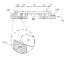
- tapered edge 240 of tapered land 228 a may be set at an angle (e.g., approximately 2-5°) relative to an axis 242 . Angle may be adapted such tapered land 228 a has minimal contact or no contact with edge 244 (i.e., flat region) of substrate 12 as shown in FIG. 22A .
- FIG. 22B illustrates another exemplary embodiment of chuck 14 a wherein chuck 14 a includes substantially planar land 228 b . Positioning of substrate 12 in single wave shape may provide outer diameter d 3 of substrate 12 at a distance g, from substantially planar land 228 b.
- template chuck 28 a may provide patterning surface 22 of template 18 to conform to single wave shape of substrate 12 during imprinting and/or separation.
- Template chuck 28 a may include throughways 254 adapted to provide a vacuum and/or pressure affecting shaping of template 18 .
- throughway(s) 254 a may provide a vacuum holding outer edge of template 18 such that outer edges of template 18 bow towards chuck 28 .
- Throughway(s) 254 b may provide vacuum and/or pressure such that center of template 18 bows towards substrate 12 . Center of template 18 may contact substrate 12 conforming to single wave shape.
- center of template 18 may contact inner diameter d 1 of substrate 12 with fluid motion of polymerizable material 34 flowing outward towards outer diameter d 3 of substrate 12 . Additionally, during separation, final separation may occur at center of template 18 and inner diameter d 1 of substrate 12 with single wave shape of substrate 12 and conforming shape of template 18 .
- template chuck 28 b may provide patterning surface 22 of template 18 in a double wave formation during imprinting and/or separation with substrate 12 having a single wave shape.
- throughways 560 a - 560 c of template chuck 28 b may provide vacuum and/or pressure to provide template 18 in a double wave formation.
- throughway 560 b may provide pressure while throughways 560 a and 560 c may provide vacuum in chambers formed by lands 562 a - 562 c (e.g., three or more chambers).
- Pressure and/or vacuum within chambers may provide template 18 in a double wave formation such that portions of template 18 in superimposition with throughway 560 b bow towards substrate 12 and portions of template 18 in superimposition with throughways 560 a and 560 c may bow away from substrate 12 .
- Portions of template 18 in superimposition with throughway 560 b may contact substrate 12 first.
- additional throughways 560 and/or chambers may be used. As illustrated in FIG. 24 b , vacuum may be reduced and/or pressure reduced such that template 18 contacts remaining portions of substrate 12 . In particular, portion of template 18 in superimposition with throughway 560 c (e.g., in superimposition with inner diameter of substrate 12 ), may contact substrate 12 last. As such, gas between template 18 and substrate 12 may be evacuated at inner diameter of substrate 12 .
- the surface of substrate 12 may be provided in a substantially well-controlled shape by substrate chuck 14 to avoid any localized fluid from spreading abnormally. Local surface adhesion between the mask 20 and the patterned surface 46 on the substrate 12 , however, may exceed the holding effort from the substrate chuck 14 . This may cause a localized bending of the substrate 12 at the boundary of the imprinted area. Such localized bending may cause a loss of vacuum holding pressure, and as such, separation may fail.
- constraint of substrate 12 may be provided by a holding system 660 in addition to, or in lieu of substrate chuck 14 .
- holding system 660 may engage substrate 12 , and by using a force F, may provide constraint of the substrate 12 during separation of patterned layer from template as described herein.
- holding system 660 surrounds substrate 12 .
- multiple holding systems 660 may be strategically placed about substrate 12 to provide constraint of the substrate 12 during separation of template 18 from substrate 12 .
- Holding system 660 may include a contact head 668 and body 669 .
- Contact head 668 may provide force F to constrain substrate 12 .
- Contact head 668 may be stationary or adjustable depending on design considerations.
- Contact head 668 may comprise a surface for contacting substrate 12 .
- Contact head 668 have at least one surface 670 at an angle T relative to body 669 such that surface 670 aligns with a portion of substrate 12 .
- surface 670 at an angle T relative to body 669 such that surface 670 aligns with a chamfered edge 664 of substrate 12 as illustrated in FIG. 26 .
- Having contact head 668 contact the chamfered edge 664 of substrate 12 may prevent interference of holding system 660 with patterned layer 46 (shown in FIG. 2 ) on substrate 12 .
- contact head 668 may provide force F to substrate 12 for constraining substrate 12 to substrate chuck 14 .
- contact head 668 may provide force F to chamfered edge 664 of substrate 12 , as illustrated in FIG. 27 , to substantially constrain substrate 12 to substrate chuck 14 during separation as described herein.
- Holding system 660 may also comprise a base 666 .
- body 669 may be adjustably attached to base 666 to provide radial motion of body 669 about the x- and y-axes. Radial motion of the body 669 about base 666 may provide distance between substrate 12 and contact head 668 for loading and unloading of substrate 12 .
- body 669 in a first position body 669 may be positioned on base 666 such that contact head 668 may be in contact with substrate 12 .
- radial motion of body 669 about base 666 may provide contact head 668 to be located a set distance D away from substrate 12 .
- the motion range of the body 669 about base 666 generally is no more than needed for loading and unloading of substrate 12 .
- motion range of body 669 about base 666 may be on the order of 50 microns to 1 mm.
- motion of body 669 about base 666 may exceed necessary requirements for general loading and unloading of substrate 12 depending on design considerations.
- base 666 may provide an additional force F C to body 669 for constraining substrate 12 during separation as described herein.
- body 669 may be adjustably attached to base 666 to provide a constraining force F C about the z-axes.
- contact head 668 may be coupled to base 666 by a vacuum preloaded air bearing, magnetic preloaded air bearing, and/or the like.
- FIG. 28 illustrates a flow chart 680 of an exemplary method for constraining substrate 12 during separation of template 18 from substrate 12 .
- substrate 12 may be loaded to system 10 .
- contact head 668 may be placed in contact with substrate 12 .
- surface 670 of contact head 668 may contact chamfered edge 664 of substrate 12 .
- contact head 668 may provide force F constraining substrate 12 .
- base 666 may provide force F C for constraining body 669 .
- the system 10 may perform the imprinting process.
- contact head 668 may be separated from substrate 12 by radial motion of body 669 about bass 666 .
- substrate 12 may be unloaded from system 10 .
Abstract
Description
Claims (16)
Priority Applications (7)
| Application Number | Priority Date | Filing Date | Title |
|---|---|---|---|
| US12/582,091 US8215946B2 (en) | 2006-05-18 | 2009-10-20 | Imprint lithography system and method |
| JP2011533171A JP5289577B2 (en) | 2008-10-23 | 2009-10-21 | Equipment with vacuum chuck for imprint lithography equipment |
| PCT/US2009/005721 WO2010047788A2 (en) | 2008-10-23 | 2009-10-21 | Imprint lithography system and method |
| SG2013079025A SG195597A1 (en) | 2008-10-23 | 2009-10-21 | Imprint lithography system and method |
| MYPI2011001704A MY165977A (en) | 2008-10-23 | 2009-10-21 | Imprint lithography system and method |
| CN2009801427660A CN102203672B (en) | 2008-10-23 | 2009-10-21 | Imprint lithography system and method |
| JP2013028729A JP5335156B2 (en) | 2008-10-23 | 2013-02-18 | Substrate holding device |
Applications Claiming Priority (6)
| Application Number | Priority Date | Filing Date | Title |
|---|---|---|---|
| US80126506P | 2006-05-18 | 2006-05-18 | |
| US82712806P | 2006-09-27 | 2006-09-27 | |
| US11/749,909 US7641840B2 (en) | 2002-11-13 | 2007-05-17 | Method for expelling gas positioned between a substrate and a mold |
| US10772908P | 2008-10-23 | 2008-10-23 | |
| US10864008P | 2008-10-27 | 2008-10-27 | |
| US12/582,091 US8215946B2 (en) | 2006-05-18 | 2009-10-20 | Imprint lithography system and method |
Related Parent Applications (1)
| Application Number | Title | Priority Date | Filing Date |
|---|---|---|---|
| US11/749,909 Continuation-In-Part US7641840B2 (en) | 2002-11-13 | 2007-05-17 | Method for expelling gas positioned between a substrate and a mold |
Publications (2)
| Publication Number | Publication Date |
|---|---|
| US20100072652A1 US20100072652A1 (en) | 2010-03-25 |
| US8215946B2 true US8215946B2 (en) | 2012-07-10 |
Family
ID=42036819
Family Applications (1)
| Application Number | Title | Priority Date | Filing Date |
|---|---|---|---|
| US12/582,091 Expired - Fee Related US8215946B2 (en) | 2006-05-18 | 2009-10-20 | Imprint lithography system and method |
Country Status (6)
| Country | Link |
|---|---|
| US (1) | US8215946B2 (en) |
| JP (2) | JP5289577B2 (en) |
| CN (1) | CN102203672B (en) |
| MY (1) | MY165977A (en) |
| SG (1) | SG195597A1 (en) |
| WO (1) | WO2010047788A2 (en) |
Cited By (12)
| Publication number | Priority date | Publication date | Assignee | Title |
|---|---|---|---|---|
| US20110049761A1 (en) * | 2009-08-31 | 2011-03-03 | Fujifilm Corporation | Pattern transfer apparatus and pattern forming method |
| US20120015065A1 (en) * | 2009-03-26 | 2012-01-19 | Marel Townsend Further Processing B.V. | Mass-distributing device and moulding device comprising a mass-distributing device of this type |
| US20120256346A1 (en) * | 2003-03-20 | 2012-10-11 | Masahiko Ogino | Mold structures, and method of transfer of fine structures |
| US20140141135A1 (en) * | 2011-05-24 | 2014-05-22 | Hendrikus Cornelis Koos van Doom | Moulding device and method for moulding a food product |
| US9653329B2 (en) | 2012-11-19 | 2017-05-16 | Ev Group E. Thallner Gmbh | Semiconductor treating device and method |
| US9682510B2 (en) | 2012-05-08 | 2017-06-20 | Canon Kabushiki Kaisha | Imprint apparatus and method of manufacturing article |
| US20180056577A1 (en) * | 2016-08-25 | 2018-03-01 | National Cheng Kung University | Flexible mold with variable thickness |
| US9921469B2 (en) | 2013-04-24 | 2018-03-20 | Canon Kabushiki Kaisha | Imprint method, imprint apparatus, and method of manufacturing article |
| WO2018075174A1 (en) * | 2016-10-18 | 2018-04-26 | Molecular Imprints, Inc. | Microlithographic fabrication of structures |
| US10335984B2 (en) * | 2014-04-09 | 2019-07-02 | Canon Kabushiki Kaisha | Imprint apparatus and article manufacturing method |
| US10359697B2 (en) * | 2015-08-04 | 2019-07-23 | Toshiba Memory Corporation | Imprinting template substrate, method for manufacturing the same, imprinting template substrate manufacturing apparatus, and method for manufacturing semiconductor apparatus |
| US11104057B2 (en) | 2015-12-11 | 2021-08-31 | Canon Kabushiki Kaisha | Imprint apparatus and method of imprinting a partial field |
Families Citing this family (22)
| Publication number | Priority date | Publication date | Assignee | Title |
|---|---|---|---|---|
| US9164375B2 (en) * | 2009-06-19 | 2015-10-20 | Canon Nanotechnologies, Inc. | Dual zone template chuck |
| JP5395756B2 (en) * | 2010-07-07 | 2014-01-22 | 株式会社東芝 | Imprint template manufacturing method and pattern forming method |
| US9864279B2 (en) * | 2010-08-05 | 2018-01-09 | Asml Netherlands B.V. | Imprint lithography |
| WO2012083578A1 (en) * | 2010-12-22 | 2012-06-28 | 青岛理工大学 | Device and method for nano-imprinting full wafer |
| JP5492162B2 (en) * | 2011-09-01 | 2014-05-14 | 株式会社日立ハイテクノロジーズ | Microstructure transfer device |
| JP2013064836A (en) * | 2011-09-16 | 2013-04-11 | Olympus Corp | Manufacturing method of mold for forming fine structure and optical element |
| KR20130085759A (en) | 2012-01-20 | 2013-07-30 | 삼성전자주식회사 | Stamp and method of fabricating stamp and imprinting method using the same |
| JP6000656B2 (en) * | 2012-05-30 | 2016-10-05 | 株式会社日立ハイテクノロジーズ | Resin stamper manufacturing apparatus and resin stamper manufacturing method |
| JP6497839B2 (en) * | 2013-11-07 | 2019-04-10 | キヤノン株式会社 | Imprint apparatus and article manufacturing method |
| TWI665513B (en) | 2013-11-08 | 2019-07-11 | 美商佳能奈米科技股份有限公司 | Low contact imprint lithography template chuck system for improved overlay correction |
| CN106462053B (en) * | 2014-04-22 | 2020-12-01 | Ev 集团 E·索尔纳有限责任公司 | Method and apparatus for imprinting nanostructures |
| US10620532B2 (en) * | 2014-11-11 | 2020-04-14 | Canon Kabushiki Kaisha | Imprint method, imprint apparatus, mold, and article manufacturing method |
| JP6774178B2 (en) * | 2015-11-16 | 2020-10-21 | キヤノン株式会社 | Equipment for processing substrates and manufacturing methods for articles |
| KR20230037681A (en) | 2016-10-20 | 2023-03-16 | 몰레큘러 임프린츠 인코퍼레이티드 | Positioning substrates in imprint lithography processes |
| JP6762853B2 (en) * | 2016-11-11 | 2020-09-30 | キヤノン株式会社 | Equipment, methods, and article manufacturing methods |
| US11454883B2 (en) * | 2016-11-14 | 2022-09-27 | Canon Kabushiki Kaisha | Template replication |
| US10969680B2 (en) * | 2016-11-30 | 2021-04-06 | Canon Kabushiki Kaisha | System and method for adjusting a position of a template |
| JP6940944B2 (en) | 2016-12-06 | 2021-09-29 | キヤノン株式会社 | Imprint device and article manufacturing method |
| TWI666128B (en) * | 2018-07-24 | 2019-07-21 | 奇景光電股份有限公司 | Measuring fixture |
| US11198235B2 (en) * | 2018-08-09 | 2021-12-14 | Canon Kabushiki Kaisha | Flexible mask modulation for controlling atmosphere between mask and substrate and methods of using the same |
| JP7410616B2 (en) | 2019-09-24 | 2024-01-10 | キヤノン株式会社 | Flattening device, article manufacturing method, flattening method, and imprint device |
| JP7418127B2 (en) | 2020-03-24 | 2024-01-19 | キヤノン株式会社 | Flattening device, flattening method, and article manufacturing method |
Citations (182)
| Publication number | Priority date | Publication date | Assignee | Title |
|---|---|---|---|---|
| US3637381A (en) | 1966-09-22 | 1972-01-25 | Teeg Research Inc | Radiation-sensitive self-revealing elements and methods of making and utilizing the same |
| US3997447A (en) | 1974-06-07 | 1976-12-14 | Composite Sciences, Inc. | Fluid processing apparatus |
| US4119688A (en) | 1975-11-03 | 1978-10-10 | International Business Machines Corporation | Electro-lithography method |
| US4233261A (en) | 1977-09-28 | 1980-11-11 | U.S. Philips Corporation | Method and device for manufacturing information carriers |
| US4279628A (en) | 1979-12-31 | 1981-07-21 | Energy Synergistics, Inc. | Apparatus for drying a natural gas stream |
| US4312823A (en) | 1977-03-14 | 1982-01-26 | U.S. Philips Corporation | Method of manufacturing a plastic record carrier having a stratified structure |
| US4395211A (en) * | 1979-08-10 | 1983-07-26 | U.S. Philips Corporation | Method and device for manufacturing a plastic record carrier |
| US4475223A (en) | 1981-06-12 | 1984-10-02 | Hitachi, Ltd. | Exposure process and system |
| US4506184A (en) * | 1984-01-10 | 1985-03-19 | Varian Associates, Inc. | Deformable chuck driven by piezoelectric means |
| US4512848A (en) | 1984-02-06 | 1985-04-23 | Exxon Research And Engineering Co. | Procedure for fabrication of microstructures over large areas using physical replication |
| US4521175A (en) | 1980-03-14 | 1985-06-04 | Multivac Sepp Haggenmuller Kg | Apparatus for producing containers from thermoplastic sheet material |
| US4551192A (en) | 1983-06-30 | 1985-11-05 | International Business Machines Corporation | Electrostatic or vacuum pinchuck formed with microcircuit lithography |
| US4559717A (en) | 1984-02-21 | 1985-12-24 | The United States Of America As Represented By The Secretary Of Commerce | Flexure hinge |
| US4689004A (en) | 1985-04-18 | 1987-08-25 | Firma Carl Freudenberg | Apparatus for adhering thermally-softenable plastic particles into a plastic body |
| US4724222A (en) | 1986-04-28 | 1988-02-09 | American Telephone And Telegraph Company, At&T Bell Laboratories | Wafer chuck comprising a curved reference surface |
| US4731155A (en) | 1987-04-15 | 1988-03-15 | General Electric Company | Process for forming a lithographic mask |
| US4767584A (en) | 1985-04-03 | 1988-08-30 | Massachusetts Institute Of Technology | Process of and apparatus for producing design patterns in materials |
| US4887282A (en) * | 1986-11-18 | 1989-12-12 | Siemens Aktiengesellschaft | Method and apparatus for changing the imaging scale in X-ray lithograph |
| US5028361A (en) | 1987-11-09 | 1991-07-02 | Takeo Fujimoto | Method for molding a photosensitive composition |
| US5028366A (en) | 1988-01-12 | 1991-07-02 | Air Products And Chemicals, Inc. | Water based mold release compositions for making molded polyurethane foam |
| US5029418A (en) * | 1990-03-05 | 1991-07-09 | Eastman Kodak Company | Sawing method for substrate cutting operations |
| US5213600A (en) | 1987-06-09 | 1993-05-25 | International Business Machines Corp. | Method of manufacturing an optical storage disk |
| US5259926A (en) | 1991-09-24 | 1993-11-09 | Hitachi, Ltd. | Method of manufacturing a thin-film pattern on a substrate |
| US5324012A (en) | 1991-07-16 | 1994-06-28 | Nikon Corporation | Holding apparatus for holding an article such as a semiconductor wafer |
| US5331371A (en) | 1990-09-26 | 1994-07-19 | Canon Kabushiki Kaisha | Alignment and exposure method |
| US5338177A (en) | 1992-04-22 | 1994-08-16 | Societe Nationale Industrielle Et Aerospatiale | Hot compacting device for the production of parts requiring simultaneous pressure and temperature rises |
| US5364222A (en) | 1992-02-05 | 1994-11-15 | Tokyo Electron Limited | Apparatus for processing wafer-shaped substrates |
| US5374829A (en) * | 1990-05-07 | 1994-12-20 | Canon Kabushiki Kaisha | Vacuum chuck |
| US5425848A (en) | 1993-03-16 | 1995-06-20 | U.S. Philips Corporation | Method of providing a patterned relief of cured photoresist on a flat substrate surface and device for carrying out such a method |
| US5512131A (en) | 1993-10-04 | 1996-04-30 | President And Fellows Of Harvard College | Formation of microstamped patterns on surfaces and derivative articles |
| US5515167A (en) | 1994-09-13 | 1996-05-07 | Hughes Aircraft Company | Transparent optical chuck incorporating optical monitoring |
| US5527662A (en) | 1990-05-24 | 1996-06-18 | Matsushita Electric Industrial Co., Ltd. | Process for forming fine pattern |
| US5534073A (en) | 1992-09-07 | 1996-07-09 | Mitsubishi Denki Kabushiki Kaisha | Semiconductor producing apparatus comprising wafer vacuum chucking device |
| US5545367A (en) | 1992-04-15 | 1996-08-13 | Soane Technologies, Inc. | Rapid prototype three dimensional stereolithography |
| US5550654A (en) | 1993-07-19 | 1996-08-27 | Lucent Technologies Inc. | Method for forming, in optical media, refractive index perturbations having reduced birefringence |
| US5563684A (en) | 1994-11-30 | 1996-10-08 | Sgs-Thomson Microelectronics, Inc. | Adaptive wafer modulator for placing a selected pattern on a semiconductor wafer |
| US5601641A (en) | 1992-07-21 | 1997-02-11 | Tse Industries, Inc. | Mold release composition with polybutadiene and method of coating a mold core |
| US5669303A (en) | 1996-03-04 | 1997-09-23 | Motorola | Apparatus and method for stamping a surface |
| US5675403A (en) * | 1994-11-22 | 1997-10-07 | Wisconsin Alumni Research Foundation | Stress-free mount for imaging mask |
| US5737064A (en) | 1994-03-15 | 1998-04-07 | Matsushita Electric Industrial Co., Ltd. | Exposure apparatus for transferring a mask pattern onto a substrate |
| US5772905A (en) | 1995-11-15 | 1998-06-30 | Regents Of The University Of Minnesota | Nanoimprint lithography |
| US5776748A (en) | 1993-10-04 | 1998-07-07 | President And Fellows Of Harvard College | Method of formation of microstamped patterns on plates for adhesion of cells and other biological materials, devices and uses therefor |
| US5804089A (en) | 1994-10-31 | 1998-09-08 | Matsushita Electric Industrial Co., Ltd. | Plasma processing apparatus and method |
| US5820769A (en) | 1995-05-24 | 1998-10-13 | Regents Of The University Of Minnesota | Method for making magnetic storage having discrete elements with quantized magnetic moments |
| US5821175A (en) | 1988-07-08 | 1998-10-13 | Cauldron Limited Partnership | Removal of surface contaminants by irradiation using various methods to achieve desired inert gas flow over treated surface |
| US5849209A (en) | 1995-03-31 | 1998-12-15 | Johnson & Johnson Vision Products, Inc. | Mold material made with additives |
| US5849222A (en) | 1995-09-29 | 1998-12-15 | Johnson & Johnson Vision Products, Inc. | Method for reducing lens hole defects in production of contact lens blanks |
| US5888120A (en) * | 1997-09-29 | 1999-03-30 | Lsi Logic Corporation | Method and apparatus for chemical mechanical polishing |
| US5900062A (en) | 1995-12-28 | 1999-05-04 | Applied Materials, Inc. | Lift pin for dechucking substrates |
| US5923408A (en) | 1996-01-31 | 1999-07-13 | Canon Kabushiki Kaisha | Substrate holding system and exposure apparatus using the same |
| US5932045A (en) * | 1997-06-02 | 1999-08-03 | Lucent Technologies Inc. | Method for fabricating a multilayer optical article |
| US5948470A (en) | 1997-04-28 | 1999-09-07 | Harrison; Christopher | Method of nanoscale patterning and products made thereby |
| US5947027A (en) | 1998-09-08 | 1999-09-07 | Motorola, Inc. | Printing apparatus with inflatable means for advancing a substrate towards the stamping surface |
| US5997963A (en) | 1998-05-05 | 1999-12-07 | Ultratech Stepper, Inc. | Microchamber |
| US6019166A (en) | 1997-12-30 | 2000-02-01 | Intel Corporation | Pickup chuck with an integral heatsink |
| US6030275A (en) * | 1998-03-17 | 2000-02-29 | International Business Machines Corporation | Variable control of carrier curvature with direct feedback loop |
| US6032506A (en) | 1996-05-30 | 2000-03-07 | S.C. Recherche Et Developpement Groupe | Improvment to the blank holder force regulating system in a press |
| US6099771A (en) | 1998-07-08 | 2000-08-08 | Lear Corporation | Vacuum compression method for forming molded thermoplastic floor mat having a "Class A" finish |
| US6137562A (en) | 1996-12-05 | 2000-10-24 | Nikon Corporation | Substrate adjuster, substrate holder and substrate holding method |
| US6159400A (en) | 1995-08-01 | 2000-12-12 | Laquer; Henry Louis | Method for deforming solids in a controlled atmosphere and at adjustable rates, pressures and temperature |
| US6160430A (en) | 1999-03-22 | 2000-12-12 | Ati International Srl | Powerup sequence artificial voltage supply circuit |
| EP1072954A2 (en) | 1999-07-28 | 2001-01-31 | Lucent Technologies Inc. | Lithographic process for device fabrication |
| US6182510B1 (en) | 1997-04-30 | 2001-02-06 | Sensys Instruments Corporation | Apparatus and method for characterizing semiconductor wafers during processing |
| US6218316B1 (en) | 1998-10-22 | 2001-04-17 | Micron Technology, Inc. | Planarization of non-planar surfaces in device fabrication |
| US6220561B1 (en) | 1999-06-30 | 2001-04-24 | Sandia Corporation | Compound floating pivot micromechanisms |
| US6247579B1 (en) | 1999-01-18 | 2001-06-19 | Tokyo Ohka Kogyo Co., Ltd | Substrate transfer apparatus and method of substrate transfer |
| US6257866B1 (en) | 1996-06-18 | 2001-07-10 | Hy-Tech Forming Systems, Inc. | Apparatus for accurately forming plastic sheet |
| US6304424B1 (en) | 1998-04-03 | 2001-10-16 | Applied Materials Inc. | Method and apparatus for minimizing plasma destabilization within a semiconductor wafer processing system |
| US6305677B1 (en) | 1999-03-30 | 2001-10-23 | Lam Research Corporation | Perimeter wafer lifting |
| US6309580B1 (en) | 1995-11-15 | 2001-10-30 | Regents Of The University Of Minnesota | Release surfaces, particularly for use in nanoimprint lithography |
| US6313567B1 (en) | 2000-04-10 | 2001-11-06 | Motorola, Inc. | Lithography chuck having piezoelectric elements, and method |
| US6334960B1 (en) | 1999-03-11 | 2002-01-01 | Board Of Regents, The University Of Texas System | Step and flash imprint lithography |
| US20020018190A1 (en) | 2000-06-15 | 2002-02-14 | Hideki Nogawa | Exposure apparatus and device manufacturing method |
| US6355198B1 (en) | 1996-03-15 | 2002-03-12 | President And Fellows Of Harvard College | Method of forming articles including waveguides via capillary micromolding and microtransfer molding |
| US20020042027A1 (en) | 1998-10-09 | 2002-04-11 | Chou Stephen Y. | Microscale patterning and articles formed thereby |
| US6383890B2 (en) | 1997-12-26 | 2002-05-07 | Canon Kabushiki Kaisha | Wafer bonding method, apparatus and vacuum chuck |
| US6391217B2 (en) | 1999-12-23 | 2002-05-21 | University Of Massachusetts | Methods and apparatus for forming submicron patterns on films |
| US20020069525A1 (en) | 2000-09-18 | 2002-06-13 | Junichi Hada | Apparatus and method for mounting components on substrate |
| US6407006B1 (en) | 1999-09-09 | 2002-06-18 | Honeywell International, Inc. | Method for integrated circuit planarization |
| US6416311B1 (en) | 1998-05-04 | 2002-07-09 | Jenoptik Aktiengesellschaft | Device and method for separating a shaped substrate from a stamping tool |
| US20020094496A1 (en) | 2000-07-17 | 2002-07-18 | Choi Byung J. | Method and system of automatic fluid dispensing for imprint lithography processes |
| US20020132482A1 (en) | 2000-07-18 | 2002-09-19 | Chou Stephen Y. | Fluid pressure imprint lithography |
| US6461524B1 (en) | 1999-05-27 | 2002-10-08 | Sanyo Electric Co., Ltd. | Method of filtering a fluid |
| US20020150398A1 (en) | 2000-08-21 | 2002-10-17 | Choi Byung J. | Flexure based macro motion translation stage |
| US6512401B2 (en) | 1999-09-10 | 2003-01-28 | Intel Corporation | Output buffer for high and low voltage bus |
| US6513796B2 (en) * | 2001-02-23 | 2003-02-04 | International Business Machines Corporation | Wafer chuck having a removable insert |
| US6518189B1 (en) | 1995-11-15 | 2003-02-11 | Regents Of The University Of Minnesota | Method and apparatus for high density nanostructures |
| US6517995B1 (en) | 1999-09-14 | 2003-02-11 | Massachusetts Institute Of Technology | Fabrication of finely featured devices by liquid embossing |
| US6538733B2 (en) * | 2000-08-22 | 2003-03-25 | Ade Corporation | Ring chuck to hold 200 and 300 mm wafer |
| US20030062334A1 (en) | 2001-09-25 | 2003-04-03 | Lee Hong Hie | Method for forming a micro-pattern on a substrate by using capillary force |
| US20030080472A1 (en) | 2001-10-29 | 2003-05-01 | Chou Stephen Y. | Lithographic method with bonded release layer for molding small patterns |
| US20030092261A1 (en) | 2000-12-04 | 2003-05-15 | Fumio Kondo | Substrate processing method |
| US6580172B2 (en) | 2001-03-02 | 2003-06-17 | Motorola, Inc. | Lithographic template and method of formation and use |
| US6612590B2 (en) | 2001-01-12 | 2003-09-02 | Tokyo Electron Limited | Apparatus and methods for manipulating semiconductor wafers |
| US20030179354A1 (en) | 1996-03-22 | 2003-09-25 | Nikon Corporation | Mask-holding apparatus for a light exposure apparatus and related scanning-exposure method |
| US20030189273A1 (en) | 2002-04-04 | 2003-10-09 | Lennart Olsson | Imprint method and device |
| US6646662B1 (en) | 1998-05-26 | 2003-11-11 | Seiko Epson Corporation | Patterning method, patterning apparatus, patterning template, and method for manufacturing the patterning template |
| US20040029041A1 (en) | 2002-02-27 | 2004-02-12 | Brewer Science, Inc. | Novel planarization method for multi-layer lithography processing |
| US6696220B2 (en) | 2000-10-12 | 2004-02-24 | Board Of Regents, The University Of Texas System | Template for room temperature, low pressure micro-and nano-imprint lithography |
| US20040036201A1 (en) | 2000-07-18 | 2004-02-26 | Princeton University | Methods and apparatus of field-induced pressure imprint lithography |
| US20040036850A1 (en) | 1999-08-19 | 2004-02-26 | Canon Kabushiki Kaisha | Substrate attracting and holding system for use in exposure apparatus |
| US20040046288A1 (en) | 2000-07-18 | 2004-03-11 | Chou Stephen Y. | Laset assisted direct imprint lithography |
| US6726195B1 (en) | 1998-10-13 | 2004-04-27 | Dek International Gmbh | Method for ensuring planarity when using a flexible, self conforming, workpiece support system |
| US6736408B2 (en) | 2002-01-25 | 2004-05-18 | Applied Materials Inc. | Rotary vacuum-chuck with venturi formed at base of rotating shaft |
| US20040110856A1 (en) | 2002-12-04 | 2004-06-10 | Young Jung Gun | Polymer solution for nanoimprint lithography to reduce imprint temperature and pressure |
| US20040129293A1 (en) | 2003-01-08 | 2004-07-08 | Eichenberger Louis C. | Flow system flush process |
| US20040132301A1 (en) | 2002-09-12 | 2004-07-08 | Harper Bruce M. | Indirect fluid pressure imprinting |
| US20040131718A1 (en) | 2000-07-18 | 2004-07-08 | Princeton University | Lithographic apparatus for fluid pressure imprint lithography |
| US20040137734A1 (en) | 1995-11-15 | 2004-07-15 | Princeton University | Compositions and processes for nanoimprinting |
| US6764386B2 (en) | 2002-01-11 | 2004-07-20 | Applied Materials, Inc. | Air bearing-sealed micro-processing chamber |
| US6771372B1 (en) | 2001-11-01 | 2004-08-03 | Therma-Wave, Inc. | Rotational stage with vertical axis adjustment |
| US20040156108A1 (en) | 2001-10-29 | 2004-08-12 | Chou Stephen Y. | Articles comprising nanoscale patterns with reduced edge roughness and methods of making same |
| US6776094B1 (en) | 1993-10-04 | 2004-08-17 | President & Fellows Of Harvard College | Kit For Microcontact Printing |
| US20040163563A1 (en) | 2000-07-16 | 2004-08-26 | The Board Of Regents, The University Of Texas System | Imprint lithography template having a mold to compensate for material changes of an underlying liquid |
| US20040192041A1 (en) | 2003-03-27 | 2004-09-30 | Jun-Ho Jeong | UV nanoimprint lithography process using elementwise embossed stamp and selectively additive pressurization |
| US20040197712A1 (en) | 2002-12-02 | 2004-10-07 | Jacobson Joseph M. | System for contact printing |
| US20040197843A1 (en) | 2001-07-25 | 2004-10-07 | Chou Stephen Y. | Nanochannel arrays and their preparation and use for high throughput macromolecular analysis |
| US20040250945A1 (en) | 2003-06-10 | 2004-12-16 | Industrial Technology Research Institute | Method for and apparatus for bonding patterned imprint to a substrate by adhering means |
| US6849558B2 (en) | 2002-05-22 | 2005-02-01 | The Board Of Trustees Of The Leland Stanford Junior University | Replication and transfer of microstructures and nanostructures |
| US20050037143A1 (en) | 2000-07-18 | 2005-02-17 | Chou Stephen Y. | Imprint lithography with improved monitoring and control and apparatus therefor |
| US20050046449A1 (en) | 2003-08-26 | 2005-03-03 | Davis Jeffrey B. | Voltage mismatch tolerant input/output buffer |
| US6869890B2 (en) | 2001-01-09 | 2005-03-22 | Ebara Corporation | Processing apparatus to be sealed against workpiece |
| US6870301B2 (en) | 1999-10-29 | 2005-03-22 | Board Of Regents, The University Of Texas System | Method of separating a template from a substrate during imprint lithography |
| US20050064054A1 (en) * | 2003-09-24 | 2005-03-24 | Canon Kabushiki Kaisha | Pattern forming apparatus |
| US20050061773A1 (en) | 2003-08-21 | 2005-03-24 | Byung-Jin Choi | Capillary imprinting technique |
| US6871558B2 (en) | 2002-12-12 | 2005-03-29 | Molecular Imprints, Inc. | Method for determining characteristics of substrate employing fluid geometries |
| US20050072757A1 (en) | 2003-10-02 | 2005-04-07 | University Of Texas System Board Of Regents | Method of creating a turbulent flow of fluid between a mold and a substrate |
| US20050106321A1 (en) | 2003-11-14 | 2005-05-19 | Molecular Imprints, Inc. | Dispense geometery to achieve high-speed filling and throughput |
| US6898064B1 (en) | 2001-08-29 | 2005-05-24 | Lsi Logic Corporation | System and method for optimizing the electrostatic removal of a workpiece from a chuck |
| US6900881B2 (en) | 2002-07-11 | 2005-05-31 | Molecular Imprints, Inc. | Step and repeat imprint lithography systems |
| US6908861B2 (en) | 2002-07-11 | 2005-06-21 | Molecular Imprints, Inc. | Method for imprint lithography using an electric field |
| US6916584B2 (en) | 2002-08-01 | 2005-07-12 | Molecular Imprints, Inc. | Alignment methods for imprint lithography |
| US6926929B2 (en) | 2002-07-09 | 2005-08-09 | Molecular Imprints, Inc. | System and method for dispensing liquids |
| US6932934B2 (en) | 2002-07-11 | 2005-08-23 | Molecular Imprints, Inc. | Formation of discontinuous films during an imprint lithography process |
| US20050189676A1 (en) | 2004-02-27 | 2005-09-01 | Molecular Imprints, Inc. | Full-wafer or large area imprinting with multiple separated sub-fields for high throughput lithography |
| US6951173B1 (en) | 2003-05-14 | 2005-10-04 | Molecular Imprints, Inc. | Assembly and method for transferring imprint lithography templates |
| US6954275B2 (en) | 2000-08-01 | 2005-10-11 | Boards Of Regents, The University Of Texas System | Methods for high-precision gap and orientation sensing between a transparent template and substrate for imprint lithography |
| US6965506B2 (en) | 1998-09-30 | 2005-11-15 | Lam Research Corporation | System and method for dechucking a workpiece from an electrostatic chuck |
| US20050270312A1 (en) | 2004-06-03 | 2005-12-08 | Molecular Imprints, Inc. | Fluid dispensing and drop-on-demand dispensing for nano-scale manufacturing |
| US20050276919A1 (en) | 2004-06-01 | 2005-12-15 | Molecular Imprints, Inc. | Method for dispensing a fluid on a substrate |
| US20050274693A1 (en) | 2004-05-07 | 2005-12-15 | Babak Heidari | Device and method for lithography |
| US6980282B2 (en) | 2002-12-11 | 2005-12-27 | Molecular Imprints, Inc. | Method for modulating shapes of substrates |
| US6982783B2 (en) | 2002-11-13 | 2006-01-03 | Molecular Imprints, Inc. | Chucking system for modulating shapes of substrates |
| US20060063112A1 (en) | 2004-09-21 | 2006-03-23 | Molecular Imprints, Inc. | Pattern reversal employing thick residual layers |
| US7018572B2 (en) | 2001-06-11 | 2006-03-28 | General Electric Company | Method for producing data storage media |
| US7023238B1 (en) | 2004-01-07 | 2006-04-04 | Altera Corporation | Input buffer with selectable threshold and hysteresis option |
| US20060076717A1 (en) | 2002-07-11 | 2006-04-13 | Molecular Imprints, Inc. | Step and repeat imprint lithography processes |
| US20060115999A1 (en) | 2004-12-01 | 2006-06-01 | Molecular Imprints, Inc. | Methods of exposure for the purpose of thermal management for imprint lithography processes |
| US20060121728A1 (en) | 2004-12-07 | 2006-06-08 | Molecular Imprints, Inc. | Method for fast filling of templates for imprint lithography using on template dispense |
| US7070405B2 (en) | 2002-08-01 | 2006-07-04 | Molecular Imprints, Inc. | Alignment systems for imprint lithography |
| US7071088B2 (en) | 2002-08-23 | 2006-07-04 | Molecular Imprints, Inc. | Method for fabricating bulbous-shaped vias |
| US20060172553A1 (en) * | 2005-01-31 | 2006-08-03 | Molecular Imprints, Inc. | Method of retaining a substrate to a wafer chuck |
| US20060172549A1 (en) * | 2005-01-31 | 2006-08-03 | Molecular Imprints, Inc. | Method of separating a mold from a solidified layer disposed on a substrate |
| US20060177535A1 (en) | 2005-02-04 | 2006-08-10 | Molecular Imprints, Inc. | Imprint lithography template to facilitate control of liquid movement |
| US20060177532A1 (en) | 2005-02-04 | 2006-08-10 | Molecular Imprints, Inc. | Imprint lithography method to control extrusion of a liquid from a desired region on a substrate |
| US7119884B2 (en) * | 2003-12-24 | 2006-10-10 | Asml Netherlands B.V. | Lithographic apparatus and device manufacturing method |
| US7150622B2 (en) | 2003-07-09 | 2006-12-19 | Molecular Imprints, Inc. | Systems for magnification and distortion correction for imprint lithography processes |
| US7179079B2 (en) | 2002-07-08 | 2007-02-20 | Molecular Imprints, Inc. | Conforming template for patterning liquids disposed on substrates |
| US20070063384A1 (en) | 2005-09-21 | 2007-03-22 | Molecular Imprints, Inc. | Method to control an atmostphere between a body and a substrate |
| US20070126150A1 (en) | 2005-12-01 | 2007-06-07 | Molecular Imprints, Inc. | Bifurcated contact printing technique |
| US20070132152A1 (en) | 2005-12-08 | 2007-06-14 | Molecular Imprints, Inc. | Method and System for Double-Sided Patterning of Substrates |
| US20070141271A1 (en) | 2004-09-23 | 2007-06-21 | Molecular Imprints, Inc. | Method for controlling distribution of fluid components on a body |
| US7245358B2 (en) | 2004-05-28 | 2007-07-17 | Board Of Regents, The University Of Texas System | Substrate support system |
| US7244386B2 (en) | 2004-09-27 | 2007-07-17 | Molecular Imprints, Inc. | Method of compensating for a volumetric shrinkage of a material disposed upon a substrate to form a substantially planar structure therefrom |
| US20070170617A1 (en) | 2006-01-20 | 2007-07-26 | Molecular Imprints, Inc. | Patterning Substrates Employing Multiple Chucks |
| US20070190200A1 (en) | 2005-01-31 | 2007-08-16 | Molecular Imprints, Inc. | Chucking system comprising an array of fluid chambers |
| US20070228593A1 (en) | 2006-04-03 | 2007-10-04 | Molecular Imprints, Inc. | Residual Layer Thickness Measurement and Correction |
| US20070228608A1 (en) | 2006-04-03 | 2007-10-04 | Molecular Imprints, Inc. | Preserving Filled Features when Vacuum Wiping |
| US20070231422A1 (en) | 2006-04-03 | 2007-10-04 | Molecular Imprints, Inc. | System to vary dimensions of a thin template |
| US7292426B2 (en) * | 2003-10-01 | 2007-11-06 | Canon Kabushiki Kaisha | Substrate holding system and exposure apparatus using the same |
| US7298456B2 (en) | 2004-06-03 | 2007-11-20 | Molecular Imprints, Inc. | System for varying dimensions of a substrate during nanoscale manufacturing |
| US7307697B2 (en) | 2004-05-28 | 2007-12-11 | Board Of Regents, The University Of Texas System | Adaptive shape substrate support system |
| US20070287081A1 (en) | 2004-06-03 | 2007-12-13 | Molecular Imprints, Inc. | Method for obtaining force combinations for template deformation using nullspace and methods optimization techniques |
| US20080141862A1 (en) | 2003-10-02 | 2008-06-19 | Molecular Imprints, Inc. | Single Phase Fluid Imprint Lithography Method |
| US7462028B2 (en) | 2006-04-03 | 2008-12-09 | Molecular Imprints, Inc. | Partial vacuum environment imprinting |
| US20080303187A1 (en) | 2006-12-29 | 2008-12-11 | Molecular Imprints, Inc. | Imprint Fluid Control |
| US20090014917A1 (en) | 2007-07-10 | 2009-01-15 | Molecular Imprints, Inc. | Drop Pattern Generation for Imprint Lithography |
| US20090115110A1 (en) | 2007-11-02 | 2009-05-07 | Molecular Imprints, Inc. | Drop Pattern Generation for Imprint Lithography |
| US20090148619A1 (en) | 2007-12-05 | 2009-06-11 | Molecular Imprints, Inc. | Controlling Thickness of Residual Layer |
| US7641840B2 (en) | 2002-11-13 | 2010-01-05 | Molecular Imprints, Inc. | Method for expelling gas positioned between a substrate and a mold |
| US20100112220A1 (en) | 2008-11-03 | 2010-05-06 | Molecular Imprints, Inc. | Dispense system set-up and characterization |
| US7780893B2 (en) | 2006-04-03 | 2010-08-24 | Molecular Imprints, Inc. | Method of concurrently patterning a substrate having a plurality of fields and a plurality of alignment marks |
Family Cites Families (21)
| Publication number | Priority date | Publication date | Assignee | Title |
|---|---|---|---|---|
| JPS59107723U (en) * | 1982-12-29 | 1984-07-20 | 富士通株式会社 | disk fixing device |
| JPS6194323A (en) * | 1984-10-16 | 1986-05-13 | Canon Inc | Apparatus for correcting surface shape of laminar plate |
| JPS6194322A (en) * | 1984-10-16 | 1986-05-13 | Canon Inc | Apparatus for correcting surface shape of laminar plate |
| JPH03504285A (en) * | 1988-05-18 | 1991-09-19 | シーメンス、アクチエンゲゼルシヤフト | How to change the projection scale of X-ray lithography |
| JPH0245951A (en) * | 1988-08-08 | 1990-02-15 | Kyushu Electron Metal Co Ltd | Holding device for semiconductor substrate |
| JPH07312194A (en) * | 1994-05-18 | 1995-11-28 | Shimadzu Corp | Analyzer device |
| US5804017A (en) * | 1995-07-27 | 1998-09-08 | Imation Corp. | Method and apparatus for making an optical information record |
| JP2000031253A (en) * | 1998-07-10 | 2000-01-28 | Komatsu Ltd | Substrate processing device and method |
| JP3862131B2 (en) * | 1999-10-14 | 2006-12-27 | 日本精工株式会社 | Proximity exposure equipment |
| US6936194B2 (en) | 2002-09-05 | 2005-08-30 | Molecular Imprints, Inc. | Functional patterning material for imprint lithography processes |
| US20040065252A1 (en) | 2002-10-04 | 2004-04-08 | Sreenivasan Sidlgata V. | Method of forming a layer on a substrate to facilitate fabrication of metrology standards |
| US8349241B2 (en) | 2002-10-04 | 2013-01-08 | Molecular Imprints, Inc. | Method to arrange features on a substrate to replicate features having minimal dimensional variability |
| EP2261966B1 (en) * | 2002-11-13 | 2012-03-14 | Molecular Imprints, Inc. | A lithographic system including a chucking system |
| US20050035514A1 (en) * | 2003-08-11 | 2005-02-17 | Supercritical Systems, Inc. | Vacuum chuck apparatus and method for holding a wafer during high pressure processing |
| KR101293059B1 (en) * | 2005-12-08 | 2013-08-05 | 몰레큘러 임프린츠 인코퍼레이티드 | Method for expelling gas positioned between a substrate and a mold |
| KR20090004910A (en) * | 2006-04-03 | 2009-01-12 | 몰레큘러 임프린츠 인코퍼레이티드 | Chucking system comprising an array of fluid chambers |
| JP2007281053A (en) * | 2006-04-04 | 2007-10-25 | Miraial Kk | Thin plate housing container |
| WO2007136832A2 (en) * | 2006-05-18 | 2007-11-29 | Molecular Imprints, Inc. | Method for expelling gas positioned between a substrate and a mold |
| JP3919022B2 (en) * | 2006-07-26 | 2007-05-23 | 日本精工株式会社 | Exposure method and mask holding method |
| US20100103402A1 (en) * | 2007-02-26 | 2010-04-29 | Dai Nippon Printing Co., Ltd | Work stage of exposing apparatus, exposing method and method of manufacturing a structure |
| JP4478164B2 (en) * | 2007-03-12 | 2010-06-09 | 株式会社日立ハイテクノロジーズ | MICROSTRUCTURE TRANSFER APPARATUS, STAMPER, AND MICROSTRUCTURE MANUFACTURING METHOD |
-
2009
- 2009-10-20 US US12/582,091 patent/US8215946B2/en not_active Expired - Fee Related
- 2009-10-21 WO PCT/US2009/005721 patent/WO2010047788A2/en active Application Filing
- 2009-10-21 JP JP2011533171A patent/JP5289577B2/en not_active Expired - Fee Related
- 2009-10-21 SG SG2013079025A patent/SG195597A1/en unknown
- 2009-10-21 MY MYPI2011001704A patent/MY165977A/en unknown
- 2009-10-21 CN CN2009801427660A patent/CN102203672B/en not_active Expired - Fee Related
-
2013
- 2013-02-18 JP JP2013028729A patent/JP5335156B2/en not_active Expired - Fee Related
Patent Citations (221)
| Publication number | Priority date | Publication date | Assignee | Title |
|---|---|---|---|---|
| US3637381A (en) | 1966-09-22 | 1972-01-25 | Teeg Research Inc | Radiation-sensitive self-revealing elements and methods of making and utilizing the same |
| US3997447A (en) | 1974-06-07 | 1976-12-14 | Composite Sciences, Inc. | Fluid processing apparatus |
| US4119688A (en) | 1975-11-03 | 1978-10-10 | International Business Machines Corporation | Electro-lithography method |
| US4312823A (en) | 1977-03-14 | 1982-01-26 | U.S. Philips Corporation | Method of manufacturing a plastic record carrier having a stratified structure |
| US4233261A (en) | 1977-09-28 | 1980-11-11 | U.S. Philips Corporation | Method and device for manufacturing information carriers |
| US4395211A (en) * | 1979-08-10 | 1983-07-26 | U.S. Philips Corporation | Method and device for manufacturing a plastic record carrier |
| US4279628A (en) | 1979-12-31 | 1981-07-21 | Energy Synergistics, Inc. | Apparatus for drying a natural gas stream |
| US4521175A (en) | 1980-03-14 | 1985-06-04 | Multivac Sepp Haggenmuller Kg | Apparatus for producing containers from thermoplastic sheet material |
| US4475223A (en) | 1981-06-12 | 1984-10-02 | Hitachi, Ltd. | Exposure process and system |
| US4551192A (en) | 1983-06-30 | 1985-11-05 | International Business Machines Corporation | Electrostatic or vacuum pinchuck formed with microcircuit lithography |
| US4506184A (en) * | 1984-01-10 | 1985-03-19 | Varian Associates, Inc. | Deformable chuck driven by piezoelectric means |
| US4512848A (en) | 1984-02-06 | 1985-04-23 | Exxon Research And Engineering Co. | Procedure for fabrication of microstructures over large areas using physical replication |
| US4559717A (en) | 1984-02-21 | 1985-12-24 | The United States Of America As Represented By The Secretary Of Commerce | Flexure hinge |
| US4767584A (en) | 1985-04-03 | 1988-08-30 | Massachusetts Institute Of Technology | Process of and apparatus for producing design patterns in materials |
| US4689004A (en) | 1985-04-18 | 1987-08-25 | Firma Carl Freudenberg | Apparatus for adhering thermally-softenable plastic particles into a plastic body |
| US4724222A (en) | 1986-04-28 | 1988-02-09 | American Telephone And Telegraph Company, At&T Bell Laboratories | Wafer chuck comprising a curved reference surface |
| US4887282A (en) * | 1986-11-18 | 1989-12-12 | Siemens Aktiengesellschaft | Method and apparatus for changing the imaging scale in X-ray lithograph |
| US4731155A (en) | 1987-04-15 | 1988-03-15 | General Electric Company | Process for forming a lithographic mask |
| US5213600A (en) | 1987-06-09 | 1993-05-25 | International Business Machines Corp. | Method of manufacturing an optical storage disk |
| US5427599A (en) | 1987-06-09 | 1995-06-27 | International Business Machines Corporation | System for stamping an optical storage disk |
| US5028361A (en) | 1987-11-09 | 1991-07-02 | Takeo Fujimoto | Method for molding a photosensitive composition |
| US5028366A (en) | 1988-01-12 | 1991-07-02 | Air Products And Chemicals, Inc. | Water based mold release compositions for making molded polyurethane foam |
| US5821175A (en) | 1988-07-08 | 1998-10-13 | Cauldron Limited Partnership | Removal of surface contaminants by irradiation using various methods to achieve desired inert gas flow over treated surface |
| US5029418A (en) * | 1990-03-05 | 1991-07-09 | Eastman Kodak Company | Sawing method for substrate cutting operations |
| US5374829A (en) * | 1990-05-07 | 1994-12-20 | Canon Kabushiki Kaisha | Vacuum chuck |
| US5527662A (en) | 1990-05-24 | 1996-06-18 | Matsushita Electric Industrial Co., Ltd. | Process for forming fine pattern |
| US5331371A (en) | 1990-09-26 | 1994-07-19 | Canon Kabushiki Kaisha | Alignment and exposure method |
| US5324012A (en) | 1991-07-16 | 1994-06-28 | Nikon Corporation | Holding apparatus for holding an article such as a semiconductor wafer |
| US5259926A (en) | 1991-09-24 | 1993-11-09 | Hitachi, Ltd. | Method of manufacturing a thin-film pattern on a substrate |
| US5364222A (en) | 1992-02-05 | 1994-11-15 | Tokyo Electron Limited | Apparatus for processing wafer-shaped substrates |
| US5545367A (en) | 1992-04-15 | 1996-08-13 | Soane Technologies, Inc. | Rapid prototype three dimensional stereolithography |
| US5338177A (en) | 1992-04-22 | 1994-08-16 | Societe Nationale Industrielle Et Aerospatiale | Hot compacting device for the production of parts requiring simultaneous pressure and temperature rises |
| US5601641A (en) | 1992-07-21 | 1997-02-11 | Tse Industries, Inc. | Mold release composition with polybutadiene and method of coating a mold core |
| US5534073A (en) | 1992-09-07 | 1996-07-09 | Mitsubishi Denki Kabushiki Kaisha | Semiconductor producing apparatus comprising wafer vacuum chucking device |
| US5425848A (en) | 1993-03-16 | 1995-06-20 | U.S. Philips Corporation | Method of providing a patterned relief of cured photoresist on a flat substrate surface and device for carrying out such a method |
| US5550654A (en) | 1993-07-19 | 1996-08-27 | Lucent Technologies Inc. | Method for forming, in optical media, refractive index perturbations having reduced birefringence |
| US5512131A (en) | 1993-10-04 | 1996-04-30 | President And Fellows Of Harvard College | Formation of microstamped patterns on surfaces and derivative articles |
| US6776094B1 (en) | 1993-10-04 | 2004-08-17 | President & Fellows Of Harvard College | Kit For Microcontact Printing |
| US5776748A (en) | 1993-10-04 | 1998-07-07 | President And Fellows Of Harvard College | Method of formation of microstamped patterns on plates for adhesion of cells and other biological materials, devices and uses therefor |
| US5737064A (en) | 1994-03-15 | 1998-04-07 | Matsushita Electric Industrial Co., Ltd. | Exposure apparatus for transferring a mask pattern onto a substrate |
| US5515167A (en) | 1994-09-13 | 1996-05-07 | Hughes Aircraft Company | Transparent optical chuck incorporating optical monitoring |
| US5804089A (en) | 1994-10-31 | 1998-09-08 | Matsushita Electric Industrial Co., Ltd. | Plasma processing apparatus and method |
| US5675403A (en) * | 1994-11-22 | 1997-10-07 | Wisconsin Alumni Research Foundation | Stress-free mount for imaging mask |
| US5563684A (en) | 1994-11-30 | 1996-10-08 | Sgs-Thomson Microelectronics, Inc. | Adaptive wafer modulator for placing a selected pattern on a semiconductor wafer |
| US5849209A (en) | 1995-03-31 | 1998-12-15 | Johnson & Johnson Vision Products, Inc. | Mold material made with additives |
| US5820769A (en) | 1995-05-24 | 1998-10-13 | Regents Of The University Of Minnesota | Method for making magnetic storage having discrete elements with quantized magnetic moments |
| US5956216A (en) | 1995-05-24 | 1999-09-21 | Regents Of The University Of Minnesota | Magnetic storage having discrete elements with quantized magnetic moments |
| US6159400A (en) | 1995-08-01 | 2000-12-12 | Laquer; Henry Louis | Method for deforming solids in a controlled atmosphere and at adjustable rates, pressures and temperature |
| US5849222A (en) | 1995-09-29 | 1998-12-15 | Johnson & Johnson Vision Products, Inc. | Method for reducing lens hole defects in production of contact lens blanks |
| US5772905A (en) | 1995-11-15 | 1998-06-30 | Regents Of The University Of Minnesota | Nanoimprint lithography |
| US20040137734A1 (en) | 1995-11-15 | 2004-07-15 | Princeton University | Compositions and processes for nanoimprinting |
| US6828244B2 (en) | 1995-11-15 | 2004-12-07 | Regents Of The University Of Minnesota | Method and apparatus for high density nanostructures |
| US6809356B2 (en) | 1995-11-15 | 2004-10-26 | Regents Of The University Of Minnesota | Method and apparatus for high density nanostructures |
| US6518189B1 (en) | 1995-11-15 | 2003-02-11 | Regents Of The University Of Minnesota | Method and apparatus for high density nanostructures |
| US6309580B1 (en) | 1995-11-15 | 2001-10-30 | Regents Of The University Of Minnesota | Release surfaces, particularly for use in nanoimprint lithography |
| US5900062A (en) | 1995-12-28 | 1999-05-04 | Applied Materials, Inc. | Lift pin for dechucking substrates |
| US5923408A (en) | 1996-01-31 | 1999-07-13 | Canon Kabushiki Kaisha | Substrate holding system and exposure apparatus using the same |
| US5669303A (en) | 1996-03-04 | 1997-09-23 | Motorola | Apparatus and method for stamping a surface |
| US6355198B1 (en) | 1996-03-15 | 2002-03-12 | President And Fellows Of Harvard College | Method of forming articles including waveguides via capillary micromolding and microtransfer molding |
| US20030179354A1 (en) | 1996-03-22 | 2003-09-25 | Nikon Corporation | Mask-holding apparatus for a light exposure apparatus and related scanning-exposure method |
| US6032506A (en) | 1996-05-30 | 2000-03-07 | S.C. Recherche Et Developpement Groupe | Improvment to the blank holder force regulating system in a press |
| US6257866B1 (en) | 1996-06-18 | 2001-07-10 | Hy-Tech Forming Systems, Inc. | Apparatus for accurately forming plastic sheet |
| US6137562A (en) | 1996-12-05 | 2000-10-24 | Nikon Corporation | Substrate adjuster, substrate holder and substrate holding method |
| US5948470A (en) | 1997-04-28 | 1999-09-07 | Harrison; Christopher | Method of nanoscale patterning and products made thereby |
| US6182510B1 (en) | 1997-04-30 | 2001-02-06 | Sensys Instruments Corporation | Apparatus and method for characterizing semiconductor wafers during processing |
| US5932045A (en) * | 1997-06-02 | 1999-08-03 | Lucent Technologies Inc. | Method for fabricating a multilayer optical article |
| US5888120A (en) * | 1997-09-29 | 1999-03-30 | Lsi Logic Corporation | Method and apparatus for chemical mechanical polishing |
| US6383890B2 (en) | 1997-12-26 | 2002-05-07 | Canon Kabushiki Kaisha | Wafer bonding method, apparatus and vacuum chuck |
| US6019166A (en) | 1997-12-30 | 2000-02-01 | Intel Corporation | Pickup chuck with an integral heatsink |
| US6030275A (en) * | 1998-03-17 | 2000-02-29 | International Business Machines Corporation | Variable control of carrier curvature with direct feedback loop |
| US6304424B1 (en) | 1998-04-03 | 2001-10-16 | Applied Materials Inc. | Method and apparatus for minimizing plasma destabilization within a semiconductor wafer processing system |
| US6416311B1 (en) | 1998-05-04 | 2002-07-09 | Jenoptik Aktiengesellschaft | Device and method for separating a shaped substrate from a stamping tool |
| US5997963A (en) | 1998-05-05 | 1999-12-07 | Ultratech Stepper, Inc. | Microchamber |
| US6646662B1 (en) | 1998-05-26 | 2003-11-11 | Seiko Epson Corporation | Patterning method, patterning apparatus, patterning template, and method for manufacturing the patterning template |
| US20030034329A1 (en) | 1998-06-30 | 2003-02-20 | Chou Stephen Y. | Lithographic method for molding pattern with nanoscale depth |
| US20020167117A1 (en) | 1998-06-30 | 2002-11-14 | Regents Of The University Of Minnesota | Release surfaces, particularly for use in nanoimprint lithography |
| US6099771A (en) | 1998-07-08 | 2000-08-08 | Lear Corporation | Vacuum compression method for forming molded thermoplastic floor mat having a "Class A" finish |
| US5947027A (en) | 1998-09-08 | 1999-09-07 | Motorola, Inc. | Printing apparatus with inflatable means for advancing a substrate towards the stamping surface |
| US6965506B2 (en) | 1998-09-30 | 2005-11-15 | Lam Research Corporation | System and method for dechucking a workpiece from an electrostatic chuck |
| US20020042027A1 (en) | 1998-10-09 | 2002-04-11 | Chou Stephen Y. | Microscale patterning and articles formed thereby |
| US6713238B1 (en) | 1998-10-09 | 2004-03-30 | Stephen Y. Chou | Microscale patterning and articles formed thereby |
| US20040118809A1 (en) | 1998-10-09 | 2004-06-24 | Chou Stephen Y. | Microscale patterning and articles formed thereby |
| US6726195B1 (en) | 1998-10-13 | 2004-04-27 | Dek International Gmbh | Method for ensuring planarity when using a flexible, self conforming, workpiece support system |
| US6218316B1 (en) | 1998-10-22 | 2001-04-17 | Micron Technology, Inc. | Planarization of non-planar surfaces in device fabrication |
| US6247579B1 (en) | 1999-01-18 | 2001-06-19 | Tokyo Ohka Kogyo Co., Ltd | Substrate transfer apparatus and method of substrate transfer |
| US6334960B1 (en) | 1999-03-11 | 2002-01-01 | Board Of Regents, The University Of Texas System | Step and flash imprint lithography |
| US20050236739A1 (en) | 1999-03-11 | 2005-10-27 | Board Of Regents, The University Of Texas System | Step and flash imprint lithography |
| US6160430A (en) | 1999-03-22 | 2000-12-12 | Ati International Srl | Powerup sequence artificial voltage supply circuit |
| US6305677B1 (en) | 1999-03-30 | 2001-10-23 | Lam Research Corporation | Perimeter wafer lifting |
| US6461524B1 (en) | 1999-05-27 | 2002-10-08 | Sanyo Electric Co., Ltd. | Method of filtering a fluid |
| US6220561B1 (en) | 1999-06-30 | 2001-04-24 | Sandia Corporation | Compound floating pivot micromechanisms |
| EP1072954A2 (en) | 1999-07-28 | 2001-01-31 | Lucent Technologies Inc. | Lithographic process for device fabrication |
| US20040036850A1 (en) | 1999-08-19 | 2004-02-26 | Canon Kabushiki Kaisha | Substrate attracting and holding system for use in exposure apparatus |
| US6809802B1 (en) * | 1999-08-19 | 2004-10-26 | Canon Kabushiki Kaisha | Substrate attracting and holding system for use in exposure apparatus |
| US6407006B1 (en) | 1999-09-09 | 2002-06-18 | Honeywell International, Inc. | Method for integrated circuit planarization |
| US6512401B2 (en) | 1999-09-10 | 2003-01-28 | Intel Corporation | Output buffer for high and low voltage bus |
| US6517995B1 (en) | 1999-09-14 | 2003-02-11 | Massachusetts Institute Of Technology | Fabrication of finely featured devices by liquid embossing |
| US6870301B2 (en) | 1999-10-29 | 2005-03-22 | Board Of Regents, The University Of Texas System | Method of separating a template from a substrate during imprint lithography |
| US6391217B2 (en) | 1999-12-23 | 2002-05-21 | University Of Massachusetts | Methods and apparatus for forming submicron patterns on films |
| US6313567B1 (en) | 2000-04-10 | 2001-11-06 | Motorola, Inc. | Lithography chuck having piezoelectric elements, and method |
| US20020018190A1 (en) | 2000-06-15 | 2002-02-14 | Hideki Nogawa | Exposure apparatus and device manufacturing method |
| US6916585B2 (en) | 2000-07-16 | 2005-07-12 | Board Of Regents, The University Of Texas Systems | Method of varying template dimensions to achieve alignment during imprint lithography |
| US20040163563A1 (en) | 2000-07-16 | 2004-08-26 | The Board Of Regents, The University Of Texas System | Imprint lithography template having a mold to compensate for material changes of an underlying liquid |
| US20040141163A1 (en) | 2000-07-16 | 2004-07-22 | The University Of Texas System, Board Of Regents, Ut System | Device for holding a template for use in imprint lithography |
| US6842229B2 (en) | 2000-07-16 | 2005-01-11 | Board Of Regents, The University Of Texas System | Imprint lithography template comprising alignment marks |
| US20020094496A1 (en) | 2000-07-17 | 2002-07-18 | Choi Byung J. | Method and system of automatic fluid dispensing for imprint lithography processes |
| US20080199816A1 (en) | 2000-07-17 | 2008-08-21 | The University Of Texas Board Of Regents | Method of Automatic Fluid Dispensing for Imprint Lithography Processes |
| US20040046288A1 (en) | 2000-07-18 | 2004-03-11 | Chou Stephen Y. | Laset assisted direct imprint lithography |
| US20050037143A1 (en) | 2000-07-18 | 2005-02-17 | Chou Stephen Y. | Imprint lithography with improved monitoring and control and apparatus therefor |
| US20040036201A1 (en) | 2000-07-18 | 2004-02-26 | Princeton University | Methods and apparatus of field-induced pressure imprint lithography |
| US20020132482A1 (en) | 2000-07-18 | 2002-09-19 | Chou Stephen Y. | Fluid pressure imprint lithography |
| US6482742B1 (en) | 2000-07-18 | 2002-11-19 | Stephen Y. Chou | Fluid pressure imprint lithography |
| US20040131718A1 (en) | 2000-07-18 | 2004-07-08 | Princeton University | Lithographic apparatus for fluid pressure imprint lithography |
| US6954275B2 (en) | 2000-08-01 | 2005-10-11 | Boards Of Regents, The University Of Texas System | Methods for high-precision gap and orientation sensing between a transparent template and substrate for imprint lithography |
| US20020150398A1 (en) | 2000-08-21 | 2002-10-17 | Choi Byung J. | Flexure based macro motion translation stage |
| US6538733B2 (en) * | 2000-08-22 | 2003-03-25 | Ade Corporation | Ring chuck to hold 200 and 300 mm wafer |
| US20020069525A1 (en) | 2000-09-18 | 2002-06-13 | Junichi Hada | Apparatus and method for mounting components on substrate |
| US6696220B2 (en) | 2000-10-12 | 2004-02-24 | Board Of Regents, The University Of Texas System | Template for room temperature, low pressure micro-and nano-imprint lithography |
| US20030092261A1 (en) | 2000-12-04 | 2003-05-15 | Fumio Kondo | Substrate processing method |
| US6869890B2 (en) | 2001-01-09 | 2005-03-22 | Ebara Corporation | Processing apparatus to be sealed against workpiece |
| US6612590B2 (en) | 2001-01-12 | 2003-09-02 | Tokyo Electron Limited | Apparatus and methods for manipulating semiconductor wafers |
| US6513796B2 (en) * | 2001-02-23 | 2003-02-04 | International Business Machines Corporation | Wafer chuck having a removable insert |
| US6580172B2 (en) | 2001-03-02 | 2003-06-17 | Motorola, Inc. | Lithographic template and method of formation and use |
| US7018572B2 (en) | 2001-06-11 | 2006-03-28 | General Electric Company | Method for producing data storage media |
| US20040197843A1 (en) | 2001-07-25 | 2004-10-07 | Chou Stephen Y. | Nanochannel arrays and their preparation and use for high throughput macromolecular analysis |
| US6898064B1 (en) | 2001-08-29 | 2005-05-24 | Lsi Logic Corporation | System and method for optimizing the electrostatic removal of a workpiece from a chuck |
| US20030062334A1 (en) | 2001-09-25 | 2003-04-03 | Lee Hong Hie | Method for forming a micro-pattern on a substrate by using capillary force |
| US20030080472A1 (en) | 2001-10-29 | 2003-05-01 | Chou Stephen Y. | Lithographic method with bonded release layer for molding small patterns |
| US20030080471A1 (en) | 2001-10-29 | 2003-05-01 | Chou Stephen Y. | Lithographic method for molding pattern with nanoscale features |
| US20040156108A1 (en) | 2001-10-29 | 2004-08-12 | Chou Stephen Y. | Articles comprising nanoscale patterns with reduced edge roughness and methods of making same |
| US6771372B1 (en) | 2001-11-01 | 2004-08-03 | Therma-Wave, Inc. | Rotational stage with vertical axis adjustment |
| US6764386B2 (en) | 2002-01-11 | 2004-07-20 | Applied Materials, Inc. | Air bearing-sealed micro-processing chamber |
| US6736408B2 (en) | 2002-01-25 | 2004-05-18 | Applied Materials Inc. | Rotary vacuum-chuck with venturi formed at base of rotating shaft |
| US20040029041A1 (en) | 2002-02-27 | 2004-02-12 | Brewer Science, Inc. | Novel planarization method for multi-layer lithography processing |
| US20030189273A1 (en) | 2002-04-04 | 2003-10-09 | Lennart Olsson | Imprint method and device |
| US7144539B2 (en) | 2002-04-04 | 2006-12-05 | Obducat Ab | Imprint method and device |
| US6849558B2 (en) | 2002-05-22 | 2005-02-01 | The Board Of Trustees Of The Leland Stanford Junior University | Replication and transfer of microstructures and nanostructures |
| US7179079B2 (en) | 2002-07-08 | 2007-02-20 | Molecular Imprints, Inc. | Conforming template for patterning liquids disposed on substrates |
| US7252715B2 (en) | 2002-07-09 | 2007-08-07 | Molecular Imprints, Inc. | System for dispensing liquids |
| US6926929B2 (en) | 2002-07-09 | 2005-08-09 | Molecular Imprints, Inc. | System and method for dispensing liquids |
| US20060076717A1 (en) | 2002-07-11 | 2006-04-13 | Molecular Imprints, Inc. | Step and repeat imprint lithography processes |
| US6900881B2 (en) | 2002-07-11 | 2005-05-31 | Molecular Imprints, Inc. | Step and repeat imprint lithography systems |
| US6908861B2 (en) | 2002-07-11 | 2005-06-21 | Molecular Imprints, Inc. | Method for imprint lithography using an electric field |
| US7077992B2 (en) | 2002-07-11 | 2006-07-18 | Molecular Imprints, Inc. | Step and repeat imprint lithography processes |
| US6932934B2 (en) | 2002-07-11 | 2005-08-23 | Molecular Imprints, Inc. | Formation of discontinuous films during an imprint lithography process |
| US20060077374A1 (en) | 2002-07-11 | 2006-04-13 | Molecular Imprints, Inc. | Step and repeat imprint lithography systems |
| US7338275B2 (en) | 2002-07-11 | 2008-03-04 | Molecular Imprints, Inc. | Formation of discontinuous films during an imprint lithography process |
| US20080174046A1 (en) | 2002-07-11 | 2008-07-24 | Molecular Imprints Inc. | Capillary Imprinting Technique |
| US7070405B2 (en) | 2002-08-01 | 2006-07-04 | Molecular Imprints, Inc. | Alignment systems for imprint lithography |
| US6916584B2 (en) | 2002-08-01 | 2005-07-12 | Molecular Imprints, Inc. | Alignment methods for imprint lithography |
| US7071088B2 (en) | 2002-08-23 | 2006-07-04 | Molecular Imprints, Inc. | Method for fabricating bulbous-shaped vias |
| US20040132301A1 (en) | 2002-09-12 | 2004-07-08 | Harper Bruce M. | Indirect fluid pressure imprinting |
| US6982783B2 (en) | 2002-11-13 | 2006-01-03 | Molecular Imprints, Inc. | Chucking system for modulating shapes of substrates |
| US7224443B2 (en) | 2002-11-13 | 2007-05-29 | Molecular Imprints, Inc. | Imprint lithography substrate processing tool for modulating shapes of substrates |
| US20070114686A1 (en) | 2002-11-13 | 2007-05-24 | Molecular Imprints, Inc. | Method for expelling gas positioned between a substrate and a mold |
| US7641840B2 (en) | 2002-11-13 | 2010-01-05 | Molecular Imprints, Inc. | Method for expelling gas positioned between a substrate and a mold |
| US7019819B2 (en) | 2002-11-13 | 2006-03-28 | Molecular Imprints, Inc. | Chucking system for modulating shapes of substrates |
| US20040197712A1 (en) | 2002-12-02 | 2004-10-07 | Jacobson Joseph M. | System for contact printing |
| US20040110856A1 (en) | 2002-12-04 | 2004-06-10 | Young Jung Gun | Polymer solution for nanoimprint lithography to reduce imprint temperature and pressure |
| US6980282B2 (en) | 2002-12-11 | 2005-12-27 | Molecular Imprints, Inc. | Method for modulating shapes of substrates |
| US6871558B2 (en) | 2002-12-12 | 2005-03-29 | Molecular Imprints, Inc. | Method for determining characteristics of substrate employing fluid geometries |
| US6990870B2 (en) | 2002-12-12 | 2006-01-31 | Molecular Imprints, Inc. | System for determining characteristics of substrates employing fluid geometries |
| US7036389B2 (en) | 2002-12-12 | 2006-05-02 | Molecular Imprints, Inc. | System for determining characteristics of substrates employing fluid geometries |
| US20040129293A1 (en) | 2003-01-08 | 2004-07-08 | Eichenberger Louis C. | Flow system flush process |
| US20040192041A1 (en) | 2003-03-27 | 2004-09-30 | Jun-Ho Jeong | UV nanoimprint lithography process using elementwise embossed stamp and selectively additive pressurization |
| US6951173B1 (en) | 2003-05-14 | 2005-10-04 | Molecular Imprints, Inc. | Assembly and method for transferring imprint lithography templates |
| US20040250945A1 (en) | 2003-06-10 | 2004-12-16 | Industrial Technology Research Institute | Method for and apparatus for bonding patterned imprint to a substrate by adhering means |
| US7150622B2 (en) | 2003-07-09 | 2006-12-19 | Molecular Imprints, Inc. | Systems for magnification and distortion correction for imprint lithography processes |
| US20050061773A1 (en) | 2003-08-21 | 2005-03-24 | Byung-Jin Choi | Capillary imprinting technique |
| US20050046449A1 (en) | 2003-08-26 | 2005-03-03 | Davis Jeffrey B. | Voltage mismatch tolerant input/output buffer |
| US20050064054A1 (en) * | 2003-09-24 | 2005-03-24 | Canon Kabushiki Kaisha | Pattern forming apparatus |
| US7292426B2 (en) * | 2003-10-01 | 2007-11-06 | Canon Kabushiki Kaisha | Substrate holding system and exposure apparatus using the same |
| US20050072757A1 (en) | 2003-10-02 | 2005-04-07 | University Of Texas System Board Of Regents | Method of creating a turbulent flow of fluid between a mold and a substrate |
| US20080141862A1 (en) | 2003-10-02 | 2008-06-19 | Molecular Imprints, Inc. | Single Phase Fluid Imprint Lithography Method |
| US7270533B2 (en) | 2003-10-02 | 2007-09-18 | University Of Texas System, Board Of Regents | System for creating a turbulent flow of fluid between a mold and a substrate |
| US7090716B2 (en) | 2003-10-02 | 2006-08-15 | Molecular Imprints, Inc. | Single phase fluid imprint lithography method |
| US20050106321A1 (en) | 2003-11-14 | 2005-05-19 | Molecular Imprints, Inc. | Dispense geometery to achieve high-speed filling and throughput |
| US7119884B2 (en) * | 2003-12-24 | 2006-10-10 | Asml Netherlands B.V. | Lithographic apparatus and device manufacturing method |
| US7023238B1 (en) | 2004-01-07 | 2006-04-04 | Altera Corporation | Input buffer with selectable threshold and hysteresis option |
| US20080153312A1 (en) | 2004-02-18 | 2008-06-26 | Molecular Imprints, Inc. | Methods for Exposure for the Purpose of Thermal Management for Imprint Lithography Processes |
| US20050189676A1 (en) | 2004-02-27 | 2005-09-01 | Molecular Imprints, Inc. | Full-wafer or large area imprinting with multiple separated sub-fields for high throughput lithography |
| US20050274693A1 (en) | 2004-05-07 | 2005-12-15 | Babak Heidari | Device and method for lithography |
| US7259833B2 (en) | 2004-05-28 | 2007-08-21 | Board Of Regents, The Universtiy Of Texas System | Substrate support method |
| US20080204693A1 (en) | 2004-05-28 | 2008-08-28 | Board Of Regents, The University Of Texas System | Substrate Support Method |
| US7245358B2 (en) | 2004-05-28 | 2007-07-17 | Board Of Regents, The University Of Texas System | Substrate support system |
| US7307697B2 (en) | 2004-05-28 | 2007-12-11 | Board Of Regents, The University Of Texas System | Adaptive shape substrate support system |
| US20050276919A1 (en) | 2004-06-01 | 2005-12-15 | Molecular Imprints, Inc. | Method for dispensing a fluid on a substrate |
| US20050270312A1 (en) | 2004-06-03 | 2005-12-08 | Molecular Imprints, Inc. | Fluid dispensing and drop-on-demand dispensing for nano-scale manufacturing |
| US7298456B2 (en) | 2004-06-03 | 2007-11-20 | Molecular Imprints, Inc. | System for varying dimensions of a substrate during nanoscale manufacturing |
| US20070287081A1 (en) | 2004-06-03 | 2007-12-13 | Molecular Imprints, Inc. | Method for obtaining force combinations for template deformation using nullspace and methods optimization techniques |
| US20060063112A1 (en) | 2004-09-21 | 2006-03-23 | Molecular Imprints, Inc. | Pattern reversal employing thick residual layers |
| US20070141271A1 (en) | 2004-09-23 | 2007-06-21 | Molecular Imprints, Inc. | Method for controlling distribution of fluid components on a body |
| US7244386B2 (en) | 2004-09-27 | 2007-07-17 | Molecular Imprints, Inc. | Method of compensating for a volumetric shrinkage of a material disposed upon a substrate to form a substantially planar structure therefrom |
| US20060115999A1 (en) | 2004-12-01 | 2006-06-01 | Molecular Imprints, Inc. | Methods of exposure for the purpose of thermal management for imprint lithography processes |
| US20060121728A1 (en) | 2004-12-07 | 2006-06-08 | Molecular Imprints, Inc. | Method for fast filling of templates for imprint lithography using on template dispense |
| US7281919B2 (en) | 2004-12-07 | 2007-10-16 | Molecular Imprints, Inc. | System for controlling a volume of material on a mold |
| US20070190200A1 (en) | 2005-01-31 | 2007-08-16 | Molecular Imprints, Inc. | Chucking system comprising an array of fluid chambers |
| US7635263B2 (en) * | 2005-01-31 | 2009-12-22 | Molecular Imprints, Inc. | Chucking system comprising an array of fluid chambers |
| US20060172549A1 (en) * | 2005-01-31 | 2006-08-03 | Molecular Imprints, Inc. | Method of separating a mold from a solidified layer disposed on a substrate |
| US7636999B2 (en) * | 2005-01-31 | 2009-12-29 | Molecular Imprints, Inc. | Method of retaining a substrate to a wafer chuck |
| US7473090B2 (en) | 2005-01-31 | 2009-01-06 | Molecular Imprints, Inc. | Imprint lithography template to facilitate control of liquid movement |
| US20060172031A1 (en) * | 2005-01-31 | 2006-08-03 | Molecular Imprints, Inc. | Chucking system for nano-manufacturing |
| US20060172553A1 (en) * | 2005-01-31 | 2006-08-03 | Molecular Imprints, Inc. | Method of retaining a substrate to a wafer chuck |
| US20060177535A1 (en) | 2005-02-04 | 2006-08-10 | Molecular Imprints, Inc. | Imprint lithography template to facilitate control of liquid movement |
| US20060177532A1 (en) | 2005-02-04 | 2006-08-10 | Molecular Imprints, Inc. | Imprint lithography method to control extrusion of a liquid from a desired region on a substrate |
| US7316554B2 (en) | 2005-09-21 | 2008-01-08 | Molecular Imprints, Inc. | System to control an atmosphere between a body and a substrate |
| US20070063384A1 (en) | 2005-09-21 | 2007-03-22 | Molecular Imprints, Inc. | Method to control an atmostphere between a body and a substrate |
| US20070126150A1 (en) | 2005-12-01 | 2007-06-07 | Molecular Imprints, Inc. | Bifurcated contact printing technique |
| US20070132152A1 (en) | 2005-12-08 | 2007-06-14 | Molecular Imprints, Inc. | Method and System for Double-Sided Patterning of Substrates |
| US7670529B2 (en) * | 2005-12-08 | 2010-03-02 | Molecular Imprints, Inc. | Method and system for double-sided patterning of substrates |
| US20070170617A1 (en) | 2006-01-20 | 2007-07-26 | Molecular Imprints, Inc. | Patterning Substrates Employing Multiple Chucks |
| US20070228593A1 (en) | 2006-04-03 | 2007-10-04 | Molecular Imprints, Inc. | Residual Layer Thickness Measurement and Correction |
| US20070231422A1 (en) | 2006-04-03 | 2007-10-04 | Molecular Imprints, Inc. | System to vary dimensions of a thin template |
| US20070228608A1 (en) | 2006-04-03 | 2007-10-04 | Molecular Imprints, Inc. | Preserving Filled Features when Vacuum Wiping |
| US7462028B2 (en) | 2006-04-03 | 2008-12-09 | Molecular Imprints, Inc. | Partial vacuum environment imprinting |
| US7780893B2 (en) | 2006-04-03 | 2010-08-24 | Molecular Imprints, Inc. | Method of concurrently patterning a substrate having a plurality of fields and a plurality of alignment marks |
| US20080303187A1 (en) | 2006-12-29 | 2008-12-11 | Molecular Imprints, Inc. | Imprint Fluid Control |
| US20090014917A1 (en) | 2007-07-10 | 2009-01-15 | Molecular Imprints, Inc. | Drop Pattern Generation for Imprint Lithography |
| US20090115110A1 (en) | 2007-11-02 | 2009-05-07 | Molecular Imprints, Inc. | Drop Pattern Generation for Imprint Lithography |
| US20090148619A1 (en) | 2007-12-05 | 2009-06-11 | Molecular Imprints, Inc. | Controlling Thickness of Residual Layer |
| US20100112220A1 (en) | 2008-11-03 | 2010-05-06 | Molecular Imprints, Inc. | Dispense system set-up and characterization |
Non-Patent Citations (31)
| Title |
|---|
| Abstract of Japanese Patent 02-24848, Jan. 26, 1990. |
| Abstract of Japanese Patent 02-92603, Aug. 12, 2004. |
| Abstract of Japanese Patent 4-148549, May 21, 1992. |
| Abstract of Japanese Patent 57-032629, Feb. 22, 1982. |
| Abstract of Japanese Patent 57-153434, Sep. 22, 1982. |
| Abstract of Japanese Patent 60-127935, Jul. 8, 1985. |
| Bailey et al., Step and Flash Imprint Lithography: Defect Analysis, Journal of Vacuum Science, B 19(6), pp. 2806-2810 Nov. 1, 2001. |
| Bailey et al., Step and Flash Imprint Lithography: Template Surface Treatment and Defect Analysis, Journal of Vacuum Science, B 18(6), pp. 3572-3577 Nov. 1, 2000. |
| Choi et al., Design of Orientation Stages for Step and Flash Imprint Lithography, Precision Engineering, pp. 192-199 Jan. 1, 2001. |
| Chou et al., Imprint Lithography with 25-Nanometer Resolution, Science vol. 272, pp. 85-87 Apr. 5, 1996. |
| Chou et al., Imprint Lithography with Sub-10 nm Feature Size and High Throughput, Microelectronic Engineering 35, pp. 237-240 Jan. 1, 1997. |
| Chou et al., Imprint of Sub-25 nm Vias and Trenches in Polymers, Appl. Phys. Lett. 67 (21) Nov. 20, 1995. |
| Chou et al., Lithographically Induced Self-assembly of Periodic Polymer Micropillar Arrays, J. Vac. Sci. Technol. B 17 (6), pp. 3197-3202 Nov. 1, 1999. |
| Chou et al., Nanoimprint Lithography, Journal of Vacuum Science Technolgoy B 14(16), pp. 4129-4133 Nov. 1, 1996. |
| Chou et al., Ultrafast and Direct Imprint of Nanostructures in Silicon, Nature, col. 417, (Jun. 2002), pp. 835-837 Jun. 1, 2002. |
| Chou, Nanoimprint Lithography and Lithographically Induced Self-Assembly, MRS Bulletin, pp. 512-517 Jul. 1, 2001. |
| Colburn et al., Characterization and Modeling of Volumetric and Mechanical Properties for Step and Flash Imprint Lithography Photopolymers, Journal of Vacuum Science Technology. vol. b. 19(6) Nov. 1, 2001. |
| Colburn et al., Development and Advantages of Step-and-Flash Lithography, Solid State Technology Jul. 1, 2001. |
| Colburn et al., Step and Flash Imprint Lithography for sub-100 nm Patterning, Proceedings of SPIE vol. 3997, pp. 453-457 Jan. 1, 2000. |
| Colburn et al., Step and Flash Imprint Lithography: A New Approach to High-Resolution Patterning, Proc. of SPIE, vol. 3676 Mar. 1, 1999. |
| Colburn, Dissertation for the Degree of Doctor of Philosophy, Step and Flash Imprint Lithography: A Low-Pressure, Room-Temperature Nanoimprint Lithography Aug. 1, 2001. |
| Feldman, Wafer Chuck for Magnification Correction in X-ray Lithography, J. Vac. Sci. Technol. B 16(6), pp. 3476-3479 Nov. 1, 1998. |
| Feynman, There's Plenty of Room at the Bottom, Dec. 1, 1959. |
| Haisma et al., Mold-assisted Nanolithography: A Process for Reliable Pattern Replication, J. Vac. Sci. Technol. B, pp. 4124-4128 Nov. 1, 1996. |
| Heidari, Nanoimprint Lithography at the 6 in. Wafer Scale, J. Vac. Sci. Technol. B 18(6), pp. 3557-3560 Nov. 1, 2000. |
| Johnson et al., Advances in Step and Flash Imprint Lithography, SPIE Microlithography Conference Feb. 23, 2003. |
| Nguyen, Asymmetric Fluid-Structure Dynamics in Nanoscale Imprint Lithography, The University of Texas at Austin, pp. 1-111 Aug. 1, 2001. |
| Schneider et al., Stripes of Partially Fluorinated Alkyl Chains: Dipolar Langmuir Monolayers, J. Chem. Phys. vol. 122, Issue 9 Mar. 1, 2005. |
| Translation of Japanese Patent 02-24848, Jan. 26, 1990. |
| Translation of Japanese Patent 02-92603, Apr. 3, 1990. |
| Xia et al., Soft Lithography, Angew. Chem. Int. Ed., pp. 550-575 Jan. 1, 1998. |
Cited By (24)
| Publication number | Priority date | Publication date | Assignee | Title |
|---|---|---|---|---|
| US20120256346A1 (en) * | 2003-03-20 | 2012-10-11 | Masahiko Ogino | Mold structures, and method of transfer of fine structures |
| US8632714B2 (en) * | 2003-03-20 | 2014-01-21 | Hitachi, Ltd. | Mold structures, and method of transfer of fine structures |
| US20120015065A1 (en) * | 2009-03-26 | 2012-01-19 | Marel Townsend Further Processing B.V. | Mass-distributing device and moulding device comprising a mass-distributing device of this type |
| US9044029B2 (en) * | 2009-03-26 | 2015-06-02 | Marel Townsend Further Processing B.V. | Mass-distributing device and moulding device comprising a mass-distributing device of this type |
| US9433238B2 (en) | 2009-03-26 | 2016-09-06 | Marel Townsend Further Processing B.V. | Mass-distributing device and moulding device comprising a mass distributing device of this type |
| US20110049761A1 (en) * | 2009-08-31 | 2011-03-03 | Fujifilm Corporation | Pattern transfer apparatus and pattern forming method |
| US8609006B2 (en) * | 2009-08-31 | 2013-12-17 | Fujifilm Corporation | Pattern transfer apparatus and pattern forming method |
| US20140141135A1 (en) * | 2011-05-24 | 2014-05-22 | Hendrikus Cornelis Koos van Doom | Moulding device and method for moulding a food product |
| US9526269B2 (en) * | 2011-05-24 | 2016-12-27 | Marel Townsend Further Procesing B.V. | Moulding device and method for moulding a food product |
| US9682510B2 (en) | 2012-05-08 | 2017-06-20 | Canon Kabushiki Kaisha | Imprint apparatus and method of manufacturing article |
| US9653329B2 (en) | 2012-11-19 | 2017-05-16 | Ev Group E. Thallner Gmbh | Semiconductor treating device and method |
| US9921469B2 (en) | 2013-04-24 | 2018-03-20 | Canon Kabushiki Kaisha | Imprint method, imprint apparatus, and method of manufacturing article |
| US10335984B2 (en) * | 2014-04-09 | 2019-07-02 | Canon Kabushiki Kaisha | Imprint apparatus and article manufacturing method |
| US10359697B2 (en) * | 2015-08-04 | 2019-07-23 | Toshiba Memory Corporation | Imprinting template substrate, method for manufacturing the same, imprinting template substrate manufacturing apparatus, and method for manufacturing semiconductor apparatus |
| US11104057B2 (en) | 2015-12-11 | 2021-08-31 | Canon Kabushiki Kaisha | Imprint apparatus and method of imprinting a partial field |
| TWI769998B (en) * | 2015-12-11 | 2022-07-11 | 日商佳能股份有限公司 | Imprint apparatus and method of imprinting a partial field |
| US20180056577A1 (en) * | 2016-08-25 | 2018-03-01 | National Cheng Kung University | Flexible mold with variable thickness |
| WO2018075174A1 (en) * | 2016-10-18 | 2018-04-26 | Molecular Imprints, Inc. | Microlithographic fabrication of structures |
| US10274823B2 (en) | 2016-10-18 | 2019-04-30 | Molecular Imprints, Inc. | Microlithographic fabrication of structures |
| CN109937127A (en) * | 2016-10-18 | 2019-06-25 | 分子印记公司 | The microlithography of structure manufactures |
| US10585350B2 (en) | 2016-10-18 | 2020-03-10 | Molecular Imprints, Inc. | Microlithographic fabrication of structures |
| US10802397B2 (en) | 2016-10-18 | 2020-10-13 | Molecular Imprints, Inc. | Microlithographic fabrication of structures |
| CN109937127B (en) * | 2016-10-18 | 2021-06-08 | 分子印记公司 | Microlithographic fabrication of structures |
| US11307493B2 (en) | 2016-10-18 | 2022-04-19 | Molecular Imprints, Inc. | Microlithographic fabrication of structures |
Also Published As
| Publication number | Publication date |
|---|---|
| SG195597A1 (en) | 2013-12-30 |
| WO2010047788A3 (en) | 2010-11-04 |
| CN102203672A (en) | 2011-09-28 |
| WO2010047788A2 (en) | 2010-04-29 |
| JP2013157607A (en) | 2013-08-15 |
| JP5335156B2 (en) | 2013-11-06 |
| JP2012507138A (en) | 2012-03-22 |
| CN102203672B (en) | 2013-11-13 |
| MY165977A (en) | 2018-05-18 |
| US20100072652A1 (en) | 2010-03-25 |
| JP5289577B2 (en) | 2013-09-11 |
Similar Documents
| Publication | Publication Date | Title |
|---|---|---|
| US8215946B2 (en) | Imprint lithography system and method | |
| US7641840B2 (en) | Method for expelling gas positioned between a substrate and a mold | |
| USRE47483E1 (en) | Template having a varying thickness to facilitate expelling a gas positioned between a substrate and the template | |
| US8033813B2 (en) | Chucking system comprising an array of fluid chambers | |
| US8282383B2 (en) | Method for expelling gas positioned between a substrate and a mold | |
| US7670530B2 (en) | Patterning substrates employing multiple chucks | |
| EP1958025B1 (en) | Method for expelling gas positioned between a substrate and a mold | |
| US9529274B2 (en) | Chucking system with recessed support feature | |
| US9164375B2 (en) | Dual zone template chuck | |
| US20070231422A1 (en) | System to vary dimensions of a thin template | |
| KR20090004910A (en) | Chucking system comprising an array of fluid chambers | |
| WO2007136832A2 (en) | Method for expelling gas positioned between a substrate and a mold | |
| TWI414418B (en) | Imprint lithography system and method | |
| JP2020043173A (en) | Molding apparatus and article manufacturing method |
Legal Events
| Date | Code | Title | Description |
|---|---|---|---|
| AS | Assignment |
Owner name: MOLECULAR IMPRINTS, INC.,TEXAS Free format text: ASSIGNMENT OF ASSIGNORS INTEREST;ASSIGNORS:GANAPATHISUBRAMANIAN, MAHADEVAN;CHOI, BYUNG-JIN;MEISSL, MARIO JOHANNES;REEL/FRAME:023501/0929 Effective date: 20091111 Owner name: MOLECULAR IMPRINTS, INC., TEXAS Free format text: ASSIGNMENT OF ASSIGNORS INTEREST;ASSIGNORS:GANAPATHISUBRAMANIAN, MAHADEVAN;CHOI, BYUNG-JIN;MEISSL, MARIO JOHANNES;REEL/FRAME:023501/0929 Effective date: 20091111 |
|
| FEPP | Fee payment procedure |
Free format text: PAYOR NUMBER ASSIGNED (ORIGINAL EVENT CODE: ASPN); ENTITY STATUS OF PATENT OWNER: LARGE ENTITY |
|
| AS | Assignment |
Owner name: MII NEWCO, INC., TEXAS Free format text: ASSIGNMENT OF JOINT OWNERSHIP;ASSIGNOR:MOLECULAR IMPRINTS, INC.;REEL/FRAME:033329/0280 Effective date: 20140710 |
|
| AS | Assignment |
Owner name: CANON NANOTECHNOLOGIES, INC., TEXAS Free format text: CHANGE OF NAME;ASSIGNOR:MOLECULAR IMPRINTS, INC.;REEL/FRAME:033400/0184 Effective date: 20140417 |
|
| AS | Assignment |
Owner name: MOLECULAR IMPRINTS, INC., TEXAS Free format text: CHANGE OF NAME;ASSIGNOR:MII NEWCO, INC.;REEL/FRAME:033449/0684 Effective date: 20140423 |
|
| AS | Assignment |
Owner name: CANON NANOTECHNOLOGIES, INC., TEXAS Free format text: ASSIGNMENT OF ASSIGNORS INTEREST;ASSIGNOR:MOLECULAR IMPRINTS, INC.;REEL/FRAME:034981/0206 Effective date: 20150216 |
|
| AS | Assignment |
Owner name: MOLECULAR IMPRINTS, INC., TEXAS Free format text: CONFIRMATORY ASSIGNMENT OF JOINT PATENT OWNERSHIP;ASSIGNOR:CANON NANOTECHNOLOGIES, INC.;REEL/FRAME:035507/0559 Effective date: 20150427 |
|
| REMI | Maintenance fee reminder mailed | ||
| LAPS | Lapse for failure to pay maintenance fees | ||
| STCH | Information on status: patent discontinuation |
Free format text: PATENT EXPIRED DUE TO NONPAYMENT OF MAINTENANCE FEES UNDER 37 CFR 1.362 |
|
| FP | Lapsed due to failure to pay maintenance fee |
Effective date: 20160710 |
|
| AS | Assignment |
Owner name: JP MORGAN CHASE BANK, N.A., NEW YORK Free format text: PATENT SECURITY AGREEMENT;ASSIGNORS:MAGIC LEAP, INC.;MOLECULAR IMPRINTS, INC.;MENTOR ACQUISITION ONE, LLC;REEL/FRAME:050138/0287 Effective date: 20190820 |
|
| AS | Assignment |
Owner name: CITIBANK, N.A., NEW YORK Free format text: ASSIGNMENT OF SECURITY INTEREST IN PATENTS;ASSIGNOR:JPMORGAN CHASE BANK, N.A.;REEL/FRAME:050967/0138 Effective date: 20191106 |