US8228091B2 - False-link protection circuit and method for utilizing same - Google Patents
False-link protection circuit and method for utilizing same Download PDFInfo
- Publication number
- US8228091B2 US8228091B2 US12/660,430 US66043010A US8228091B2 US 8228091 B2 US8228091 B2 US 8228091B2 US 66043010 A US66043010 A US 66043010A US 8228091 B2 US8228091 B2 US 8228091B2
- Authority
- US
- United States
- Prior art keywords
- false
- protection circuit
- link
- link protection
- differential
- Prior art date
- Legal status (The legal status is an assumption and is not a legal conclusion. Google has not performed a legal analysis and makes no representation as to the accuracy of the status listed.)
- Expired - Fee Related
Links
Images


Classifications
-
- H—ELECTRICITY
- H04—ELECTRIC COMMUNICATION TECHNIQUE
- H04B—TRANSMISSION
- H04B3/00—Line transmission systems
- H04B3/02—Details
- H04B3/30—Reducing interference caused by unbalance current in a normally balanced line
-
- H—ELECTRICITY
- H04—ELECTRIC COMMUNICATION TECHNIQUE
- H04L—TRANSMISSION OF DIGITAL INFORMATION, e.g. TELEGRAPHIC COMMUNICATION
- H04L25/00—Baseband systems
- H04L25/02—Details ; arrangements for supplying electrical power along data transmission lines
- H04L25/0264—Arrangements for coupling to transmission lines
- H04L25/0272—Arrangements for coupling to multiple lines, e.g. for differential transmission
Definitions
- the present invention is generally in the field of electronic circuits and systems. More specifically, the present invention is in the field of communication circuits and systems.
- a client system that is false-linked to an electronic network may undermine the robustness of the electronic network. Under a false-link condition, a client system appears to actively communicate with the electronic network even though the client system is powered down. A false-linked client system may erroneously appear to transmit or receive data, may disrupt electronic communications and may fail interoperability specifications.
- the circuit topology of a client system may contribute to a false-link condition. Even when a client system is powered down, pulse currents from the electronic network may transfer through the client system as feedthrough currents. The feedthrough currents may activate devices within the client system and make the client system appear to communicate with the electronic network. Conventional link protection mechanisms have proven insufficient to limit these feedthrough currents or prevent a false-link condition from undermining the integrity of an electronic network.
- the false-link protection circuit should enhance interoperability of the client system with the electronic network and should be compatible with existing semiconductor manufacturing and packaging technology.
- a false-link protection circuit and method for utilizing same substantially as shown in and/or described in connection with at least one of the figures, as set forth more completely in the claims.
- FIG. 1 shows a block diagram of an exemplary network environment suitable for implementation of one embodiment of the present invention.
- FIG. 2 shows a shows a conventional line-driver circuit.
- FIG. 3 shows a line-driver circuit including a false-link protection circuit, according to one embodiment of the present invention.
- FIG. 4 shows a more detailed view of a false-link protection circuit, according to one embodiment of the present invention.
- FIG. 5 is a flowchart presenting a method for attenuating a pulse link signal, according to one embodiment of the present invention.
- the present invention is directed to a false-link protection circuit and method for utilizing same.
- the principles of the invention, as defined by the claims appended herein, can obviously be applied beyond the specifically described embodiments of the invention described herein.
- certain details have been left out in order to not obscure the inventive aspects of the invention. The details left out are within the knowledge of a person of ordinary skill in the art.
- FIG. 1 shows a block diagram of exemplary network environment 100 .
- FIG. 1 provides an overview and elements shown in FIG. 1 conceptually represent physical and electrical elements.
- network environment 100 may contain remote system 170 and client system 180 .
- Remote system 170 and client system 180 may reside on the same computer or printed circuit board, or on different nodes of a data, telecommunications, or other network, for example.
- Remote system 170 may be connected to client system 180 through a communication link, illustrated in FIG. 1 as transmission link 104 and reception link 102 .
- Transmission link 104 and reception link 102 may each comprise single-ended lines or differential lines.
- Remote system 170 may contain far-end transceiver 172 , which may send or receive data from remote system 170 through transmission link 104 and reception link 102 .
- Client system 180 may contain near-end transceiver 182 to send and receive data over the respective communication links.
- Near-end transceiver 182 may include an analog front-end unit (not pictured in FIG. 1 ) as well as analog and digital components as are known in the art.
- near-end transceiver 182 may contain low noise amplifiers, control circuitry, signal converters, and other circuits.
- Near-end transceiver 182 may also contain line-driver circuit 110 to increase the quality of an entering signal before the entering signal is used by client system 180 or transmitted via transmission link 104 .
- line-driver circuit 110 may appear to be linked to remote system 170 , despite being in a powered down state, i.e. a problem known as false-link in the art.
- conventional line-driver circuit 210 may include differential switches 214 and 222 , differential pair 230 and bias transistor 238 .
- Differential switch 214 may include metal-oxide-semiconductor field-effect transistors (“MOSFETs”) 216 and 220 connected to common source node 218 .
- differential switch 222 may include MOSFETs 224 and 228 connected to common source node 226 .
- Differential pair 230 may contain MOSFETs 232 and 236 connected to common source node 234 .
- MOSFETs 216 , 220 , 224 , 228 , 232 , 236 and 238 are illustrated as N type metal-oxide-semiconductor (“NMOS”) transistors, but may be P type metal oxide semiconductor (“P-MOS”) transistors or other types of transistors as are known in the art.
- Conventional line-driver circuit 210 may include control terminals 212 a , 212 b , 212 c , 212 d and 212 e .
- Conventional line-driver circuit 210 may also comprise positive transmission terminal 204 a , positive reception terminal 202 a , negative transmission terminal 204 b and negative reception terminal 202 b.
- MOSFETs 216 , 220 , 224 and 228 may create parasitic bipolar junction transistors (“BJTs”) that provide at least two unwanted conduction paths for current to travel through conventional line-driver circuit 210 .
- BJTs parasitic bipolar junction transistors
- each of MOSFETs 216 , 220 , 224 and 228 typically contains a parasitic BJT between its drain, channel and source regions, a configuration which may conduct current between a communication terminal of a differential switch and a common source of the differential switch.
- the physical layout of differential switches 214 and 222 can create parasitic BJTs between the respective transmission terminal, the chip substrate and the respective reception terminal of each differential switch.
- All of these parasitic BJTs may allow a pulse link signal present at communication terminals 204 a , 202 a , 204 b or 202 b to feed through conventional line-driver circuit 210 when conventional line-driver circuit 210 is powered down, e.g., is in an OFF state. More specifically, when conventional line-driver circuit 210 is powered down, a differential voltage present at communication terminals 204 a , 202 a , 204 b or 202 b is not known to correspond to transmission or reception data from conventional line-driver circuit 210 .
- a differential voltage present at, for example, positive transmission terminal 204 a and negative transmission terminal 204 b may pass through the parasitic BJTs of conventional line-driver circuit 210 and transfer to positive reception terminal 202 a and negative reception terminal 202 b , respectively.
- the feed-through current may register at positive reception terminal 202 a and negative reception terminal 202 b as a signal to link conventional line-driver circuit 210 to the far-end transceiver even though conventional line-driver circuit 210 is powered OFF.
- a negative pulse link signal present at positive reception terminal 202 a and negative reception terminal 202 b may similarly register at positive transmission terminal 204 a and negative transmission terminal 204 b as a signal to link to the far-end transceiver even though conventional line-driver circuit 210 is powered OFF.
- conventional line-driver circuit 210 would appear falsely linked to a network even though the circuit is powered OFF.
- a false-link condition may disrupt electronic communications within the network environment and may cause conventional line-driver circuit 210 to fail interoperability specifications that are required to integrate various components across an electronic platform.
- FIG. 3 illustrates exemplary line-driver circuit 310 according to an embodiment of the present invention.
- Exemplary line-driver circuit 310 may be integrated into one semiconductor die or an Ethernet physical layer (“EPHY”) as is known in the art.
- the circuit of FIG. 3 may also be integrated into an EPHY with a cascoded differential switch configuration, as a cost reduced EPHY, for example.
- line-driver circuit 310 may comprise differential switch 314 with MOSFETs 316 and 320 , and common source-node 318 .
- Line-driver circuit 310 may also comprise differential switch 322 with MOSFETs 324 and 328 , and common source node 326 .
- Exemplary line-driver circuit 310 may include bias MOSFET 338 , differential pair 330 (with MOSFETs 332 and 336 and common source node 334 ), and control terminals 312 a , 312 b , 312 c , 312 d and 312 e.
- line-driver circuit 310 comprises a plurality of communication terminals including positive transmission terminal 304 a , positive reception terminal 302 a , negative transmission terminal 304 b and negative reception terminal 302 b .
- Positive transmission terminal 304 a , positive reception terminal 302 a , negative transmission terminal 304 b and negative reception terminal 302 b may correspond to differential inputs of transmission link 104 and reception link 102 in FIG. 1 .
- MOSFETs 316 , 320 , 324 and 328 as well as differential switches 314 and 322 in FIG. 3 may be characterized by respective parasitic BJTs.
- Exemplary line-driver circuit 310 may comprise first diversionary circuit 340 a connected to common source 318 of differential switch 314 .
- Line-driver circuit 310 may further comprise second diversionary circuit 340 b connected to common source 326 of differential switch 322 .
- each of first diversionary circuit 340 a and second diversionary circuit 340 b may include a diversionary device connected between a respective common source node and ground.
- first diversionary circuit 340 a may include first diversionary transistor 342 a with grounded gate and source nodes.
- second diversionary circuit 340 b may include second diversionary transistor 342 b with grounded gate and source nodes.
- diversionary circuits 340 a and 340 b may comprise alternative diversionary devices.
- a diversionary reverse-biased diode clamp coupling one or both of respective common source nodes 318 and 326 could replace one or both of diversionary transistors 342 a and 342 b.
- Line-driver circuit 310 may also include first false-link protection circuit 350 a connected to positive transmission terminal 304 a and negative transmission terminal 304 b .
- Exemplary line-driver circuit 310 may further include second false-link protection circuit 350 b connected to positive reception terminal 302 a and negative reception terminal 302 b .
- First false-link protection circuit 350 a and second false-link protection circuit 350 b may be implemented alone or in conjunction with one another.
- FIG. 4 shows an exemplary configuration of false-link protection circuit 450 , which may correspond to either first false-link protection circuit 350 a or to second false-link protection circuit 350 b in FIG. 3 .
- false-link protection circuit 450 comprises native switch 452 , which may be a native NMOS transistor, for example. Native switch 452 may have its gate connected to ground terminal 468 .
- False-link protection circuit 450 may also include passive termination networks 456 a and 456 b .
- Passive termination networks 456 a and 456 b may each comprise termination resistors 458 and may act to protect native switch 452 and match the line impedance when the differential switches are powered up.
- passive termination network 456 a can couple the source of native switch 452 to positive terminal 462
- passive termination network 456 b can couple the drain of native switch 452 to negative terminal 464 .
- Positive terminal 462 may correspond to positive transmission terminal 304 a , in FIG. 3 , when negative terminal 464 corresponds to negative transmission terminal 304 b in that previous figure, for example.
- Positive terminal 462 may correspond to positive reception terminal 302 a when negative terminal 464 corresponds to negative reception terminal 302 b.
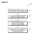
- FIG. 5 describes the steps, according to one embodiment of the present invention, of a method for attenuating a pulse link signal. It is noted that certain details and features have been left out of flowchart 500 that are apparent to a person of ordinary skill in the art. For example, a step may comprise one or more substeps as known in the art. While steps 510 through 540 indicated in flowchart 500 are sufficient to describe one embodiment of the present invention, other embodiments of the invention may utilize steps different from those shown in flowchart 500 .
- step 510 comprises activating a native switch of a false-link protection circuit by powering down a pair of differential switches.
- first false-link protection circuit 350 a and second false-link protection circuit 350 b may be activated when differential switches 314 and 322 are powered OFF. More specifically, as shown in FIG. 4 , during regular operation of the line-driver circuit the voltage at the source terminal of native switch 452 will exceed one threshold voltage value over the grounded gate voltage. In such case, native switch 452 will be in an OFF state.
- the line driver circuit when the line driver circuit is powered OFF, the voltage at the source terminal of native switch 452 need not exceed one threshold voltage value over the grounded gate voltage. That is, once the differential switches connected to false-link protection circuit 452 are powered OFF, the source voltage of native switch 452 may transition to a value that is less than one threshold voltage over the grounded gate voltage. Native switch 452 within false-link protection circuit 450 may therefore be activated when the pair of differential switches is powered down.
- step 520 comprises receiving a pulse link signal at a communication terminal of the pair of differential switches.
- a pulse link signal may be received from a far-end transceiver by one of positive transmission terminal 304 a , positive reception terminal 302 a , negative transmission terminal 304 b or negative reception terminal 302 b .
- the positive component of the pulse link signal may be received by positive terminal 462 of false-link protection circuit 450
- the negative component of the pulse link signal may be received by negative terminal 464 of false-link protection circuit 450 .
- step 530 comprises diverting a portion of the pulse link signal away from the pair of differential switches by the false-link protection circuit when the pair of differential switches is in a powered down state.
- first false-link protection circuit 350 a or second false-link protection circuit 350 b may divert a portion of a pulse link signal away from differential switches 314 and 322 .
- the pulse link signal may create a potential difference across positive terminal 462 and negative terminal 464 of false-link protection circuit 450 .
- passive termination networks 456 a and 456 b may bias the source and drain terminals of native switch 452 to conduct a portion of the pulse link signal and thus attenuate a portion of the pulse link signal. A portion of the pulse link signal may therefore be diverted away when the pair of differential switches is in a powered down state.
- step 540 comprises diverting another portion of the pulse link signal away from the common source of at least one switch of the pair of differential switches, thereby further attenuating the pulse link signal.
- the portions of the pulse link signal that did not dissipate though first false-link protection circuit 350 a and second false-link protection circuit 350 b may still flow through a differential switch.
- a portion of the pulse link signal may flow through first differential switch 314 or second differential switch 322 .
- a diversionary circuit or diversionary device may connect to a common source of a differential switch.
- first diversionary transistor 342 a may be connected to common source 318 of first differential switch 314 .
- second diversionary transistor 342 b may be connected to common source 326 of second differential switch 322 .
- First diversionary transistor 342 a may then conduct a portion of the pulse link signal away from common source 318 of differential switch 314 to ground.
- second diversionary transistor 342 b may conduct a portion of the pulse link signal away from common source 326 of differential switch 322 to ground. Accordingly, first diversionary transistor 342 a and second diversionary transistor 342 b may serve to further attenuate a portion of the pulse link signal.
- the present invention discloses a novel and inventive false-link protection circuit and method for utilizing same.
- the present invention can limit feedthrough currents and can reduce the possibility of a false-link to a far-end transceiver without undue fabrication cost or waste of semiconductor die area.
- the present invention may also maintain performance specifications of front-end transceivers and EPHYs.
- the present invention therefore presents significant advantages without adversely affecting return loss, interface specifications and system response specifications, including specifications related to rise-time response and fall-time response.
- the present invention is applicable to the design and development of EPHYs, including EPHYs with cascoded differential switches and cost reduced EPHYs.
Abstract
Description
Claims (20)
Priority Applications (1)
| Application Number | Priority Date | Filing Date | Title |
|---|---|---|---|
| US12/660,430 US8228091B2 (en) | 2010-02-25 | 2010-02-25 | False-link protection circuit and method for utilizing same |
Applications Claiming Priority (1)
| Application Number | Priority Date | Filing Date | Title |
|---|---|---|---|
| US12/660,430 US8228091B2 (en) | 2010-02-25 | 2010-02-25 | False-link protection circuit and method for utilizing same |
Publications (2)
| Publication Number | Publication Date |
|---|---|
| US20110204967A1 US20110204967A1 (en) | 2011-08-25 |
| US8228091B2 true US8228091B2 (en) | 2012-07-24 |
Family
ID=44476017
Family Applications (1)
| Application Number | Title | Priority Date | Filing Date |
|---|---|---|---|
| US12/660,430 Expired - Fee Related US8228091B2 (en) | 2010-02-25 | 2010-02-25 | False-link protection circuit and method for utilizing same |
Country Status (1)
| Country | Link |
|---|---|
| US (1) | US8228091B2 (en) |
Families Citing this family (1)
| Publication number | Priority date | Publication date | Assignee | Title |
|---|---|---|---|---|
| US10498301B2 (en) | 2018-04-27 | 2019-12-03 | Taiwan Semiconductor Manufacturing Co., Ltd. | Line drivers for wireline transmission devices |
Citations (6)
| Publication number | Priority date | Publication date | Assignee | Title |
|---|---|---|---|---|
| US20020130767A1 (en) * | 2000-11-09 | 2002-09-19 | Broadcom Corporation | IP telephone system |
| US6833734B2 (en) * | 2000-10-26 | 2004-12-21 | Broadcom Corporation | Line-driver with power down loopback protection |
| US20050024088A1 (en) * | 2003-08-01 | 2005-02-03 | Samsung Electronics Co., Ltd. | Level shifter for detecting grounded power-supply and level shifting method |
| US20070139086A1 (en) * | 2005-12-16 | 2007-06-21 | Chih-Min Liu | Transmitter and Transmission Circuit |
| US20070247209A1 (en) * | 2006-04-19 | 2007-10-25 | Chuen-Shiu Chen | Voltage level shifter apparatus |
| US20080088374A1 (en) * | 2006-10-13 | 2008-04-17 | Mediatek Inc. | Variable gain amplifiers |
-
2010
- 2010-02-25 US US12/660,430 patent/US8228091B2/en not_active Expired - Fee Related
Patent Citations (6)
| Publication number | Priority date | Publication date | Assignee | Title |
|---|---|---|---|---|
| US6833734B2 (en) * | 2000-10-26 | 2004-12-21 | Broadcom Corporation | Line-driver with power down loopback protection |
| US20020130767A1 (en) * | 2000-11-09 | 2002-09-19 | Broadcom Corporation | IP telephone system |
| US20050024088A1 (en) * | 2003-08-01 | 2005-02-03 | Samsung Electronics Co., Ltd. | Level shifter for detecting grounded power-supply and level shifting method |
| US20070139086A1 (en) * | 2005-12-16 | 2007-06-21 | Chih-Min Liu | Transmitter and Transmission Circuit |
| US20070247209A1 (en) * | 2006-04-19 | 2007-10-25 | Chuen-Shiu Chen | Voltage level shifter apparatus |
| US20080088374A1 (en) * | 2006-10-13 | 2008-04-17 | Mediatek Inc. | Variable gain amplifiers |
Also Published As
| Publication number | Publication date |
|---|---|
| US20110204967A1 (en) | 2011-08-25 |
Similar Documents
| Publication | Publication Date | Title |
|---|---|---|
| US7468638B1 (en) | Transmit/receive switch device | |
| US7088166B1 (en) | LVDS input circuit with extended common mode range | |
| US20160241140A1 (en) | High-Frequency Switching Circuit | |
| US20070290744A1 (en) | Radio frequency switching circuit, radio frequency switching device, and transmitter module device | |
| US7675329B2 (en) | Transmitter and control method for same | |
| CN109714234B (en) | Transceiver unit for transmitting data via a differential bus | |
| WO2019078994A1 (en) | T-coil enhanced esd protection with passive equalization | |
| US9921596B2 (en) | Power supply noise reduction circuit and power supply noise reduction method | |
| US20020177417A1 (en) | Transmit/receive switch for an RF transceiver | |
| US20120243712A1 (en) | Switch and switch circuit using the same | |
| US8135357B1 (en) | Integrated transmitter/receiver switch with impedance matching network | |
| US20140084997A1 (en) | Transmit/receive switch with series, doubly-floating device and switched bias voltage | |
| US8228091B2 (en) | False-link protection circuit and method for utilizing same | |
| US6944239B2 (en) | CMOS receiver for simultaneous bi-directional links | |
| US20190045675A1 (en) | Apparatuses for implementing cold-sparable serdes | |
| US6396326B1 (en) | High voltage driver having overshoot/undershoot protection circuitry | |
| US20170264281A1 (en) | Low side output driver reverse current protection circuit | |
| JP2004215230A (en) | Circuit device operable under high voltage | |
| US6646489B1 (en) | Device for switching radio frequency signals | |
| US7982491B2 (en) | Active termination and switchable passive termination circuits | |
| US20140065984A1 (en) | Transmit-receive switching circuit and wireless device | |
| CN109891758B (en) | Circuit and method for virtual mixing for full duplex transmission | |
| US20100014856A1 (en) | System and method of blocking an electrical signal transmission | |
| US6445220B1 (en) | Method and apparatus for fully-differential half-circulator for bi-directional small-signal signaling | |
| CN113037320B (en) | High-resistance state control circuit for RS-485 transceiver |
Legal Events
| Date | Code | Title | Description |
|---|---|---|---|
| AS | Assignment |
Owner name: BROADCOM CORPORATION, CALIFORNIA Free format text: ASSIGNMENT OF ASSIGNORS INTEREST;ASSIGNORS:WONG, ARK-CHEW;AZIZ, JOSEPH;TAM, DEREK;AND OTHERS;SIGNING DATES FROM 20100222 TO 20100224;REEL/FRAME:024075/0595 |
|
| AS | Assignment |
Owner name: BANK OF AMERICA, N.A., AS COLLATERAL AGENT, NORTH CAROLINA Free format text: PATENT SECURITY AGREEMENT;ASSIGNOR:BROADCOM CORPORATION;REEL/FRAME:037806/0001 Effective date: 20160201 Owner name: BANK OF AMERICA, N.A., AS COLLATERAL AGENT, NORTH Free format text: PATENT SECURITY AGREEMENT;ASSIGNOR:BROADCOM CORPORATION;REEL/FRAME:037806/0001 Effective date: 20160201 |
|
| REMI | Maintenance fee reminder mailed | ||
| LAPS | Lapse for failure to pay maintenance fees | ||
| STCH | Information on status: patent discontinuation |
Free format text: PATENT EXPIRED DUE TO NONPAYMENT OF MAINTENANCE FEES UNDER 37 CFR 1.362 |
|
| FP | Lapsed due to failure to pay maintenance fee |
Effective date: 20160724 |
|
| AS | Assignment |
Owner name: AVAGO TECHNOLOGIES GENERAL IP (SINGAPORE) PTE. LTD., SINGAPORE Free format text: ASSIGNMENT OF ASSIGNORS INTEREST;ASSIGNOR:BROADCOM CORPORATION;REEL/FRAME:041706/0001 Effective date: 20170120 Owner name: AVAGO TECHNOLOGIES GENERAL IP (SINGAPORE) PTE. LTD Free format text: ASSIGNMENT OF ASSIGNORS INTEREST;ASSIGNOR:BROADCOM CORPORATION;REEL/FRAME:041706/0001 Effective date: 20170120 |
|
| AS | Assignment |
Owner name: BROADCOM CORPORATION, CALIFORNIA Free format text: TERMINATION AND RELEASE OF SECURITY INTEREST IN PATENTS;ASSIGNOR:BANK OF AMERICA, N.A., AS COLLATERAL AGENT;REEL/FRAME:041712/0001 Effective date: 20170119 |