US8242489B2 - OLED with high efficiency blue light-emitting layer - Google Patents

OLED with high efficiency blue light-emitting layer Download PDF

Info

Publication number
US8242489B2
US8242489B2 US12/640,100 US64010009A US8242489B2 US 8242489 B2 US8242489 B2 US 8242489B2 US 64010009 A US64010009 A US 64010009A US 8242489 B2 US8242489 B2 US 8242489B2
Authority
US
United States
Prior art keywords
electron
transporting layer
layer
anthracene
oled device
Prior art date
Legal status (The legal status is an assumption and is not a legal conclusion. Google has not performed a legal analysis and makes no representation as to the accuracy of the status listed.)
Active, expires
Application number
US12/640,100
Other versions
US20110147716A1 (en
Inventor
Marina E. Kondakova
Ralph H. Young
Current Assignee (The listed assignees may be inaccurate. Google has not performed a legal analysis and makes no representation or warranty as to the accuracy of the list.)
Global OLED Technology LLC
Original Assignee
Global OLED Technology LLC
Priority date (The priority date is an assumption and is not a legal conclusion. Google has not performed a legal analysis and makes no representation as to the accuracy of the date listed.)
Filing date
Publication date
Application filed by Global OLED Technology LLC filed Critical Global OLED Technology LLC
Priority to US12/640,100 priority Critical patent/US8242489B2/en
Assigned to EASTMAN KODAK COMPANY reassignment EASTMAN KODAK COMPANY ASSIGNMENT OF ASSIGNORS INTEREST (SEE DOCUMENT FOR DETAILS). Assignors: YOUNG, RALPH H., KONDAKOVA, MARINA E.
Assigned to GLOBAL OLED TECHNOLOGY LLC reassignment GLOBAL OLED TECHNOLOGY LLC ASSIGNMENT OF ASSIGNORS INTEREST (SEE DOCUMENT FOR DETAILS). Assignors: EASTMAN KODAK COMPANY
Priority to EP10838128.6A priority patent/EP2512798B1/en
Priority to PCT/US2010/059440 priority patent/WO2011075359A1/en
Priority to CN201080056848.6A priority patent/CN102712170B/en
Priority to KR1020127015404A priority patent/KR101668044B1/en
Priority to JP2012544621A priority patent/JP5778689B2/en
Priority to TW099143241A priority patent/TWI493017B/en
Publication of US20110147716A1 publication Critical patent/US20110147716A1/en
Publication of US8242489B2 publication Critical patent/US8242489B2/en
Application granted granted Critical
Active legal-status Critical Current
Adjusted expiration legal-status Critical

Links

Images

Classifications

    • HELECTRICITY
    • H10SEMICONDUCTOR DEVICES; ELECTRIC SOLID-STATE DEVICES NOT OTHERWISE PROVIDED FOR
    • H10KORGANIC ELECTRIC SOLID-STATE DEVICES
    • H10K50/00Organic light-emitting devices
    • H10K50/10OLEDs or polymer light-emitting diodes [PLED]
    • H10K50/11OLEDs or polymer light-emitting diodes [PLED] characterised by the electroluminescent [EL] layers
    • HELECTRICITY
    • H10SEMICONDUCTOR DEVICES; ELECTRIC SOLID-STATE DEVICES NOT OTHERWISE PROVIDED FOR
    • H10KORGANIC ELECTRIC SOLID-STATE DEVICES
    • H10K50/00Organic light-emitting devices
    • H10K50/10OLEDs or polymer light-emitting diodes [PLED]
    • H10K50/14Carrier transporting layers
    • H10K50/16Electron transporting layers
    • H10K50/166Electron transporting layers comprising a multilayered structure
    • HELECTRICITY
    • H10SEMICONDUCTOR DEVICES; ELECTRIC SOLID-STATE DEVICES NOT OTHERWISE PROVIDED FOR
    • H10KORGANIC ELECTRIC SOLID-STATE DEVICES
    • H10K85/00Organic materials used in the body or electrodes of devices covered by this subclass
    • H10K85/60Organic compounds having low molecular weight
    • H10K85/615Polycyclic condensed aromatic hydrocarbons, e.g. anthracene
    • HELECTRICITY
    • H10SEMICONDUCTOR DEVICES; ELECTRIC SOLID-STATE DEVICES NOT OTHERWISE PROVIDED FOR
    • H10KORGANIC ELECTRIC SOLID-STATE DEVICES
    • H10K2101/00Properties of the organic materials covered by group H10K85/00
    • H10K2101/30Highest occupied molecular orbital [HOMO], lowest unoccupied molecular orbital [LUMO] or Fermi energy values
    • HELECTRICITY
    • H10SEMICONDUCTOR DEVICES; ELECTRIC SOLID-STATE DEVICES NOT OTHERWISE PROVIDED FOR
    • H10KORGANIC ELECTRIC SOLID-STATE DEVICES
    • H10K2101/00Properties of the organic materials covered by group H10K85/00
    • H10K2101/40Interrelation of parameters between multiple constituent active layers or sublayers, e.g. HOMO values in adjacent layers
    • HELECTRICITY
    • H10SEMICONDUCTOR DEVICES; ELECTRIC SOLID-STATE DEVICES NOT OTHERWISE PROVIDED FOR
    • H10KORGANIC ELECTRIC SOLID-STATE DEVICES
    • H10K85/00Organic materials used in the body or electrodes of devices covered by this subclass
    • H10K85/30Coordination compounds
    • H10K85/341Transition metal complexes, e.g. Ru(II)polypyridine complexes
    • H10K85/342Transition metal complexes, e.g. Ru(II)polypyridine complexes comprising iridium
    • HELECTRICITY
    • H10SEMICONDUCTOR DEVICES; ELECTRIC SOLID-STATE DEVICES NOT OTHERWISE PROVIDED FOR
    • H10KORGANIC ELECTRIC SOLID-STATE DEVICES
    • H10K85/00Organic materials used in the body or electrodes of devices covered by this subclass
    • H10K85/60Organic compounds having low molecular weight
    • H10K85/631Amine compounds having at least two aryl rest on at least one amine-nitrogen atom, e.g. triphenylamine

Definitions

  • This invention relates to an electroluminescent device, more specifically, an organic light-emitting diode (OLED) device having a light-emitting layer containing a blue light-emitting styrylamine compound and an anthracene host; a thin first electron-transporting layer; and a second electron-transporting layer consisting essentially of an anthracene.
  • the first electron-transporting layer contains a compound with a LUMO level less negative than the LUMO level of the anthracene of the second electron-transporting layer.
  • organic electroluminescent (EL) devices have been known for over two decades, their performance limitations have represented a barrier to many desirable applications.
  • organic light-emitting diodes also referred to as organic electroluminescent devices, contain spaced electrodes separated by an organic light-emitting structure which emits light in response to the application of an electrical potential difference across the electrodes.
  • At least one of the electrodes is light-transmissive, and the organic light-emitting structure can have multiple layers of organic thin films which provide for hole injection and transport from an anode, and for electron injection and transport from a cathode, respectively, with light emission resulting from electron-hole recombination at or near the internal junction formed at the interface between the hole-transporting and the electron-transporting thin films.
  • EL devices in recent years has expanded to include not only single color emitting devices, such as red, green and blue, but also devices that emit white light.
  • Efficient white light producing OLED devices are highly desirable in the industry and are considered as a low cost alternative for several applications such as paper-thin light sources, backlights in LCD displays, automotive dome lights, and office lighting.
  • White light producing OLED devices should be bright, efficient, and generally have Commission International de l'Eclairage (CIE) 1931 chromaticity coordinates of about (0.33, 0.33).
  • CIE Commission International de l'Eclairage
  • white light is that light which is perceived by a user as having a white color. Typical color combinations that produce white light are red, green and blue; blue-green and orange; blue and yellow; but others are known.
  • organic EL device components such as blue light emitting layers
  • blue light emitting layers are particularly beneficial for white-light-producing OLEDs since blue light emitters tend to have lower efficiencies than emitters of other colors, so that in order to produce balanced whites, the blue pixel (in a RGB OLED device) may need to be driven at higher current densities, resulting in increased power consumption as well as shortened blue lifetimes, and the color-complementary layer(s) (in a white OLED) may need to operate at less than their maximum potential efficiency.
  • Styrylamines are well known emitters of blue light.
  • Anthracenes are well known as electron-transporting materials (for example, see U.S. Pat. No. 6,387,546) useful as hosts in light-emitting layers (for example, see U.S. Pat. No. 5,935,721) including those with styrylamine emitters (for examples, see U.S. Pat. No. 6,534,199, U.S. Pat. No. 7,252,893, U.S. Pat. No. 7,504,526 and U.S. Pat. No. 6,713,192).
  • US Patent Publication 2007/0252522 discloses OLED devices with a blue light-emitting layer (LEL) with a styrylamine emitter and an anthracene host where the electron-transporting layer (ETL), which is located in contact with the LEL, consists of an anthracene.
  • LEL blue light-emitting layer
  • ETL electron-transporting layer
  • US Patent Publication 2007/0075631 discloses OLEDs with a thin electron-impeding layer between the LEL, which is preferably phosphorescent, and the ETL, where the materials in the thin layer can be hole-transporting and have a LUMO level that is less negative than the LUMO levels of the ETL and the host in the LEL.
  • U.S. Pat. No. 7,018,723 discloses OLEDs with ETLs that contain naphthalene and benzene derivatives.
  • Lee et al., Applied Physics Letters, 92(20), 203305/1-3 (2008) discloses OLEDs with ETLs that contain silylated benzene derivatives.
  • the invention provides an OLED device comprising an anode, a cathode and a light-emitting layer located therebetween, said light-emitting layer comprising an anthracene host and a styrylamine blue light-emitting compound; and located between the said light-emitting layer and the cathode, a first electron-transporting layer that is greater than 0.5 nm and less than 5 nm thick, and a second electron-transporting layer consisting essentially of an anthracene, located between the first electron-transporting layer and the cathode.
  • the first electron-transporting layer includes a compound with a less negative LUMO level than the LUMO level of the anthracene in the second electron-transporting layer.
  • Devices of the invention provide improved features such as increased efficiency while maintaining sufficient operational stability and excellent color characteristics.
  • FIG. 1 shows a schematic cross-sectional view of one embodiment of an inventive OLED device. It will be understood that FIG. 1 is not to scale since the individual layers are too thin and the thickness differences of various layers are too great to permit depiction to scale.
  • An OLED device of the invention is a multilayer electroluminescent device comprising a cathode, an anode, light-emitting layer(s) (LEL), electron-transporting layers (ETLs) and optionally additional layers such as electron-injecting layer(s) (EIL), hole-injecting layer(s) (HIL), hole-transporting layer(s) (HTL), exciton-blocking layer(s), spacer layer(s), connecting layer(s) and hole-blocking layer(s).
  • LEL light-emitting layer
  • ETLs electron-transporting layers
  • EIL electron-injecting layer(s)
  • HIL hole-injecting layer(s)
  • HTL hole-transporting layer(s)
  • exciton-blocking layer(s) spacer layer(s)
  • the LEL of the invention is a blue light-emitting layer. This means that at least 80% of the light emitted from this layer is blue light which has a wavelength less than 500 nm.
  • the thickness of the blue LEL is not critical, but generally between 0.5 and 50 nm, desirably between 10 and 35 nm.
  • the blue light-emitting layer of the invention comprises a host material and a blue light-emitting material.
  • the majority host material is an anthracene.
  • the host material is non-emitting; that is, produces no significant (less than 10% of the total) proportion of the light emitted by that layer.
  • the anthracene(s) should be the predominant host material(s) and present in greater percentage by volume than the other host materials.
  • the anthracene host of the invention is according to Formula (I).
  • R 1 and R 6 each independently represent an aryl group having 6-24 carbon atoms such as a phenyl group or a naphthyl group.
  • R 2 -R 5 and R 7 -R 10 are each independently chosen from hydrogen, alkyl groups of 1-24 carbon atoms or aromatic groups (including heterocyclic aromatic groups) of 5-24 carbon atoms.
  • R 1 and R 6 each represent an independently selected phenyl group, biphenyl group, or naphthyl group. It is preferred that at least one of R 1 and R 6 is naphthyl and most preferred that both are naphthyl.
  • R 3 represents hydrogen or an aromatic group of 6-24 carbon atoms and R 2 , R 4 , R 5 , R 7 -R 10 represent hydrogen.
  • a particularly preferred anthracene is one where both R 1 and R 6 are naphthyl, R 3 is aryl and R 2 , R 4 , R 5 , R 7 -R 10 represent hydrogen.
  • the blue light-emitting layer of the invention also contains a styrylamine as a blue light-emitting compound.
  • the styrylamine should be the predominating light-emitting material in that layer.
  • predominating it is meant that at least 90% of the total amount of light emitted by this layer is produced by the compound; preferably, it should be the only detectable light-emitter in this layer.
  • the styrylamine is present at 0.1% to 20% by volume of the LEL, desirably from 1% to 10%.
  • Preferred styrylamines are according to Formula (II):
  • R 1 , R 2 , R 3 and R 4 are independently chosen aryl groups of 6-24 nucleus carbon atoms with the proviso that R 1 and R 2 or R 3 and R 4 can be joined together to form a ring; or alkyl groups of 1-6 carbon atoms;
  • R 5 is selected from alkyl and aryl groups
  • n 0-4;
  • R 6 and R 7 are independently selected from hydrogen, alkyl or aryl groups
  • Ar represents a substituted or unsubstituted aryl group of 6 to 30 nucleus carbon atoms.
  • R 1 or R 2 can also be connected with R 5 to form a ring system or that R 3 or R 4 (or both) can be connected with Ar to form a ring system.
  • More preferred styrylamines are those in which R 1 , R 2 , R 3 and R 4 are substituted or unsubstituted phenyl or naphthyl groups or where (R 1 and R 2 ) or (R 3 and R 4 ) are joined together to form a carbazole group.
  • R 1 , R 2 , R 3 and R 4 is p-methylphenyl (p-tolyl).
  • R 5 can be alkyl of 1-10 carbon atoms (for example, t-butyl) or aryl groups of 6-20 nucleus carbon atoms. Adjacent R 5 substituents can also be combined to form an additional fused ring system. However, it is preferred that n is 0.
  • R 6 and R 7 can be the same alkyl or aryl groups as defined for R 5 , it is preferred that both are hydrogen.
  • Preferred Ar groups are substituted or unsubstituted phenyl, biphenyl, styryl or naphthyl.
  • Preferred substituents for Ar include styryl and phenyl.
  • Ar is a biphenyl group according to Formula (IIa):
  • Ar 1 -Ar 4 are each independently an aryl group of 6 to 24 nucleus carbon atoms where Ar 1 -Ar 2 and Ar 3 -Ar 4 can be optionally joined together to form a ring system.
  • Ar 1 -Ar 4 groups are phenyl, naphthyl, anthracenyl, fluoranthenyl, pyrenyl, and phenanthryl.
  • Ar 1 and Ar 2 or Ar 3 and Ar 4 can be joined to form a carbazole group.
  • Ar 1 -Ar 4 groups are each individually unsubstituted phenyl or alkyl substituted phenyl.
  • Methyl groups are particularly preferred alkyl substituents for when Ar 1 -Ar 4 are alkyl substituted phenyl.
  • OLEDs of the invention have a thin first ETL (denoted ETL 1 ) located between the blue LEL and the cathode along with a second ETL (denoted ETL 2 ) consisting essentially of an electron-transporting anthracene derivative that is located between the ETL 1 and the cathode.
  • ETL 1 first ETL
  • ETL 2 second ETL
  • Anthracene ETLs have many desirable properties, but when used in contact with a blue LEL that has an anthracene host, the efficiency can be less than optimal.
  • the ETL 1 contains a compound with a LUMO energy that is higher (less negative) than the LUMO energy of the anthracene used in the ETL 2 .
  • the terms LUMO level, LUMO value and LUMO energy are used synonymously herein. Without being restricted to the following theory, it is believed that this difference in LUMO energies results in a bather for injection of electrons from the ETL 2 into the ETL 1 , which causes a change in the electric field profile in the light-emitting layer. As a consequence, it is further believed that the recombination zone shifts away from the HTL/LEL interface towards the cathode side of the LEL or broadens towards the cathode side of the LEL. It is yet further believed that the shift or broadening of the recombination zone is responsible for the improved efficiency of the inventive devices, although the detailed mechanism of the improvement is not understood.
  • the ETL 1 In order to reduce voltage increase due to the presence of a barrier to electron injection and an additional layer between the ETL 2 and the LEL, this additional layer must be thin. Therefore, the ETL 1 should be less than 5 nm thick. However, it cannot be so thin as to be ineffective as a bather. Thus, the ETL 1 should be more than 0.5 nm thick. Preferably, the ETL 1 should be between 1 and 4 nm thick and ideally between 2 and 3 nm thick.
  • the ETL 1 is located between and in contact with both the blue LEL on one side (towards the anode) and the ETL 2 on the other side (towards the cathode).
  • This arrangement corresponds to the specific partial structure of anode/ . . . /blue LEL/ETL 1 /ETL 2 / . . . /cathode.
  • there can be additional layers between the ETL 2 and the cathode such as additional ETL(s) and electron-injection layers.
  • the material with the higher (less negative) LUMO should be present at 50% or more, or even more desirably 90% or more, by volume of all materials in the layer.
  • the additional component(s) should be an anthracene at 10% by volume or less.
  • Suitable anthracenes for this usage are the same as those used as hosts in the LEL according to Formula (I) and can be the same or different from the anthracene host in the LEL or the anthracene in the ETL 2 .
  • the ETL 1 is not directly adjacent to the blue LEL but is separated from it by an additional layer consisting essentially of an anthracene.
  • This layer is believed to serve primarily to transport electrons and will be denoted ETL 3 .
  • Suitable anthracenes for this usage are the same as those used as hosts in the LEL according to Formula (I).
  • the anthracene in the ETL 3 is identical to that used in the ETL 2 .
  • the ETL 1 should be between and in contact with both the ETL 3 and the ETL 2 . This corresponds to the specific partial structure of anode/ . . . /blue LEL/ETL 3 /ETL 1 /ETL 2 / . . .
  • the total thickness of the ETL 3 /ETL 1 /ETL 2 unit can be in the range of 1-50 nm, preferably between 5 and 30 nm. Although the thickness of ETL 2 and ETL 3 can be the same, it is not required, and the relative thickness of both can be varied to optimize performance.
  • Suitable materials for use in the ETL 1 having a LUMO level higher (less negative) than the LUMO level of the anthracene used in the ETL 2 are derivatives of benzene and naphthalene as well as organometallic compounds of iridium.
  • the difference between the LUMO levels of the material in the ETL 1 and the anthracene in the ETL 2 is indicative of the energy barrier for electron injection and provides the benefits of the invention.
  • the difference in LUMO levels should be at least 0.26 eV or, more preferably, it should exceed 0.35 eV.
  • the LUMO level (energy) for any compound can often be experimentally determined using well-known techniques (see, for examples, U.S. Pat. No. 7,132,174 B2, U.S. Pat. No. 7,128,982 B2, US Patent Publication 2006/0246315 or U.S. Pat. No. 7,045,952 B2) or can be calculated from theory. If possible, the HOMO (highest occupied molecular orbital) and LUMO (lowest unoccupied molecular orbital) energies of a compound should be experimentally determined for this invention. Experimentally determined LUMO energy data shown in the Table A for specific compounds were evaluated by the cyclic voltammetry method. Each LUMO energy was evaluated by adding 4.8 eV to the reduction potential vs.
  • s.c.e. saturated calomel electrode
  • a solvent mixture of acetonitrile and toluene 50%/50% v/v, i.e., 1:1 acetonitrile/toluene by volume
  • 0.1M TBAF tetrabutylammonium tetrafluoroborate
  • E Hraw is the raw energy of the HOMO
  • E Lraw is the raw energy of the LUMO
  • all quantities are expressed in electron volts (eV).
  • Values of E Hraw and E Lraw are obtained using the B3 ⁇ YP method as implemented in the Gaussian 98 (Gaussian, Inc., Pittsburgh, Pa.) computer program.
  • the basis set for use with the B3 ⁇ YP method is defined as follows: MIDI! for all atoms for which MIDI! is defined, 6-31 ⁇ * for all atoms defined in 6-31 ⁇ * but not in MIDI!, and either the LACV3 ⁇ or the LANL2 ⁇ Z basis set and pseudopotential for atoms not defined in MIDI!
  • LUMO energies differing by less than 0.05 should be considered equal for the purposes of this invention.
  • the calculated LUMO energies are also shown in Table A.
  • the experimentally determined values generally agree well with the calculated numbers.
  • the LUMO values for the materials of the invention should be experimentally determined and calculated LUMO values should be used only when it is not possible to experimentally determine the LUMO values. In any case, experimental values should be compared only to other experimental values and calculated values compared only to calculated values.
  • One class of suitable materials for the ETL 1 is benzene derivatives according to Formula (III):
  • R 8 -R 11 both represent hydrogen or substituted carbon, silicon or nitrogen atoms with the proviso that no more than two of R 8 -R 11 are hydrogen.
  • R 9′ and R 10′ are both tri-substituted silicon atoms or both di-substituted nitrogen atoms. While R 9′ and R 10′ can be different, it is preferred that they are identical. Suitable examples of tri-substituted silicon atoms are triphenylsilyl, tri-t-butylsilyl and diphenylnaphthylsilyl. Suitable examples of di-substituted nitrogen atoms are diphenylamino, di(p-methylphenyl)amino, N-phenyl-N-1-naphthylamino and heterocycles like carbazolyl.
  • R 8 -R 11 in formula (III) both represent substituted carbon atoms
  • the preferred benzene derivatives are those where R 8 -R 10 are all substituted carbon atoms as shown in Formula (IIIb):
  • R 8* -R 10* are tetrasubstituted or aromatic carbon atoms.
  • R 11* can be a hydrogen or a tetrasubstituted or aromatic carbon atom.
  • suitable aromatic carbon atoms are carbon atoms belonging to substituted or unsubstituted phenyl, naphthyl, or fluorenyl ring systems.
  • naphthalene derivatives Another class of suitable materials for the ETL 1 is naphthalene derivatives.
  • useful naphthalene derivatives are those with no additional fused aromatic rings and whose substituents are attached to the core naphthyl nucleus via single bonds.
  • Suitable naphthyl derivatives are according to Formula (IV):
  • R 12 is an aromatic substituent and p is 2 to 8.
  • Suitable materials for the ETL 1 is cyclometallated organometallic complexes of iridium. Although such a compound is often used as a phosphorescent dopant in a LEL, in the present usage it should not emit any significant amount of light (less than 10% of the total amount of light from the device). When used as the single material in a layer in any OLED, such a compound generally emits weakly if at all, because of a phenomenon known as concentration quenching. Further, contact with an anthracene in the adjoining LEL or ETL 2 favors energy transfer to the anthracene, tending to suppress any remaining emission. For iridium complexes that emit green or greater wavelength light, any emission from an ETL 1 containing the iridium complex can easily be determined from examination of the EL light output. Suitable iridium complexes are according to Formula (V):
  • M is iridium
  • A is a substituted or unsubstituted heterocyclic ring containing at least one nitrogen atom
  • B is a substituted or unsubstituted aromatic or heteroaromatic ring, or ring containing a vinyl or aromatic carbon bonded to M;
  • X—Y is an anionic bidentate ligand
  • n is an integer from 1 to 3 and
  • Compounds according to Formula (V) can be referred to as C,N- (or C ⁇ N-) cyclometallated complexes to indicate that the central metal atom is contained in a cyclic unit formed by bonding the metal atom to carbon and nitrogen atoms of one or more ligands.
  • heterocyclic ring A in formula (V) include substituted or unsubstituted pyridine, quinoline, isoquinoline, pyrimidine, indole, indazole, thiazole, and oxazole rings.
  • Examples of ring B in Formula (V) include substituted or unsubstituted phenyl, napthyl, thienyl, benzothienyl, furanyl rings.
  • Ring B in formula (V) can also be a N-containing ring such as pyridine, with the proviso that this N-containing ring bonds to M through a C atom as shown in formula (V), and not through a N atom.
  • tris-C,N-cyclometallated iridium complexes are tris(2-phenyl-4-t-butylpyridinato-N,C 2 )iridium(III) (Ir(tbuppy) 3 ), tris(2-(4′-methylphenyl)pyridinato-N,C 2′ )iridium(III), tris(3-phenylisoquinolinato-N,C 2′ )iridium(III), tris(2-phenylquinolinato-N,C 2′ )iridium(III), tris(1-(4′-methylphenyl)isoquinolinato-N,C 2′ )iridium(III), tris(2-(4′,6′-difluorophenyl)-pyridinato-N,C 2′ )iridium(III), tris(2-((5′-phenyl)-phenyl)pyridinato-N,C 2 )iridium(III),
  • Suitable iridium complexes also include compounds according to formula (V) wherein the monoanionic bidentate ligand X—Y is another C,N-cyclometallating ligand.
  • Examples include bis(1-phenylisoquinolinato-N,C 2′ )(2-phenylpyridinato-N,C 2′ )iridium(III) and bis(2-phenylpyridinato-N,C 2′ ) (1-phenylisoquinolinato-N,C 2′ )iridium(III).
  • Suitable iridium complexes according to Formula (V) can, in addition to the C,N-cyclometallating ligand(s), also contain monoanionic bidentate ligand(s) X—Y that are not C,N-cyclometallating.
  • monoanionic bidentate ligand(s) X—Y that are not C,N-cyclometallating.
  • Common examples are beta-diketonates such as acetylacetonate, and Schiff bases such as picolinate.
  • Examples of such mixed ligand complexes according to formula (V) include bis(2-phenylpyridinato-N,C 2′ )iridium(III)(acetylacetonate), bis(2-(2′-benzothienyl)pyridinato-N,C 3′ )iridium(III)(acetylacetonate), and bis(2-(4,6′-difluorophenyl)-pyridinato-N,C 2′ )iridium(III)(picolinate).
  • iridium complexes that can be suitably used in the ETL 1 should be selected according their LUMO levels from this broad list.
  • the devices of the invention contain an ETL 2 which is located between the ETL 1 and the cathode and which consists essentially of an anthracene.
  • the function of this layer is to transport electrons. Ideally, this layer is located in direct contact to the cathode side of the ETL 1 .
  • Suitable anthracenes for this usage are the same as those used as hosts in the LEL according to Formula (I). Although a mixture of anthracenes can be used, it is desirable for simplicity that a single anthracene is used.
  • anthracene consists essentially of an anthracene
  • this layer is composed of anthracene derivatives except that it can contain small and insignificant amounts of other materials such as not to materially affect the basic electrical properties that would characterize the layer in their absence.
  • the ETL 2 is composed of at least 99% of a single anthracene derivative.
  • the total thickness of the (optional ETL3)/ETL1/ETL 2 unit can be in the range of 1-50 nm, preferably between 5 and 30 nm, so that the thickness of the ETL 2 should be no more than about 49.5 nm, and desirably less than about 29.5 nm.
  • an additional electron-injection layer (EIL) or layers present between the ETL 2 and the cathode.
  • EIL electron-injection layer
  • suitable materials for the electron-injection layer include, but are not limited to, phenanthrolines (such as 4,7-diphenyl-1,10-phenanthroline (Bphen)), organic alkali metal or alkaline earth salts (such as lithium 8-hydroxyquinolate (LiQ), tris(quinolin-8-olato)aluminum(III) (Alq) or its derivatives), inorganic salts (such as LiF) or combinations thereof.
  • the electron-injection layer can also be doped with metals such as lithium.
  • the EL device emits white light, in which case the device typically includes one or more emitters of complementary color(s).
  • the device would comprise a layer with a blue fluorescent emitter together with proper proportions of a yellow emitting layer, or a combination of green and red emitting layers, suitable to make white emission.
  • This invention can be used in so-called stacked device architecture, for example, as taught in U.S. Pat. No. 5,703,436 and U.S. Pat. No. 6,337,492.
  • Embodiments of the current invention can be used in stacked devices that comprise solely fluorescent elements to produce white light.
  • the blue LEL of the invention is a fluorescent layer.
  • the white device can also include combinations of fluorescent emitting materials and phosphorescent emitting materials (sometimes referred to as hybrid OLED devices).
  • white emission can be produced by one or more hybrid blue fluorescent/red phosphorescent elements stacked in series with a green phosphorescent element using p/n junction connectors as disclosed in Tang et al. U.S. Pat. No. 6,936,961 B2.
  • White-emitting OLEDs may be used with suitable color filters to produce colored light for the pixels of a display device.
  • the EL device is part of a display device. In another suitable embodiment, the EL device is part of an area lighting device.
  • the EL device of the invention is useful in any device where stable light emission is desired such as a lamp or a component in a static or motion imaging device, such as a television, cell phone, DVD player, or computer monitor.
  • substituent group when a substituent group contains substitutable hydrogen, it is also intended to encompass not only the substituent's unsubstituted form, but also its form further substituted with any substituent group or groups as herein mentioned, so long as the substituent does not destroy properties necessary for device utility. If desired, the substituents can themselves be further substituted one or more times with the described substituent groups.
  • the particular substituents used can be selected by those skilled in the art to attain desirable properties for a specific application and can include, for example, electron-withdrawing groups, electron-donating groups, and groups providing steric bulk. When a molecule can have two or more substituents, the substituents can be joined together to form a ring such as a fused ring unless otherwise provided.
  • the present invention can be employed in many OLED configurations using small molecule materials, oligomeric materials, polymeric materials, or combinations thereof. These include from very simple structures having a single anode and cathode to more complex devices, such as passive matrix displays having orthogonal arrays of anodes and cathodes to form pixels, and active-matrix displays where each pixel is controlled independently, for example, with thin film transistors (TFTs).
  • TFTs thin film transistors
  • OLED 100 contains a substrate 110 , an anode 120 , a hole-injecting layer 130 , a hole-transporting layer 132 , a light-emitting layer (LEL) 134 , a thin first electron-transporting layer (ETL 1 ) 135 , a second electron-transporting layer (ETL 2 ) 136 , an electron-injecting layer (EIL) 138 and a cathode 140 .
  • LEL light-emitting layer
  • ETL 1 thin first electron-transporting layer
  • ETL 2 second electron-transporting layer
  • EIL electron-injecting layer
  • the LEL 134 contains the inventive combination of anthracene host and styrylamine dopant, with thin layer 135 representing the inventive ETL 1 with the material that has a less negative LUMO level than the anthracene in the ETL 2 , and ETL 136 representing the ETL 2 .
  • the substrate 110 can alternatively be located adjacent to the cathode 140 , or the substrate can actually constitute the anode 120 or cathode 140 .
  • the total combined thickness of the organic layers is preferably less than 500 nm.
  • the EIL ( 138 ) can be subdivided into two or more sublayers, namely a first electron-injecting layer (EIL 1 ) adjacent to the ETL 2 ( 136 ) and a second electron-injecting layer (ETL 2 ) located between the EIL 1 and the cathode.
  • the HIL ( 130 ) can be subdivided into two or more sublayers, namely a first hole-injecting layer (HIL 1 ) between the anode and the HTL, and a second hole-injecting layer (HIL 2 ) between the HIL 1 and the anode.
  • the anode 120 and cathode 140 of the OLED are connected to a voltage/current source 150 , through electrical conductors 160 . Applying an electrical potential difference between the anode 120 and cathode 140 such that the anode is at a more positive potential than the cathode operates the OLED. Holes are injected into the organic light-emitting structure from the anode 120 . Electrons are injected from the cathode 140 . Enhanced device stability can sometimes be achieved when the OLED is operated in an AC mode where, for some time period in a cycle, the potential bias is reversed and no current flows. An example of an AC driven OLED is described in U.S. Pat. No. 5,552,678.
  • LELs For full color display, the pixelation of LELs can be needed. This pixelated deposition of LELs is achieved using shadow masks, integral shadow masks, U.S. Pat. No. 5,294,870, spatially defined thermal dye transfer from a donor sheet, U.S. Pat. Nos. 5,688,551, 5,851,709, and 6,066,357 and an inkjet method, U.S. Pat. No. 6,066,357.
  • OLEDs of this invention can employ various well-known optical effects in order to enhance their emissive properties if desired. These include optimizing layer thicknesses to yield improved light extraction, providing dielectric mirror structures, replacing reflective electrodes with light-absorbing electrodes, providing anti-glare or anti-reflection coatings over the display, providing a polarizing medium over the display, or providing colored, neutral density, or color-conversion filters over the display. Filters, polarizers, and anti-glare or anti-reflection coatings can be specifically provided over the OLED or as part of the OLED.
  • Embodiments of the invention can provide EL devices that have good luminance efficiency, good operational stability, excellent color and low drive voltages. Embodiments of the invention can be produced consistently and with high reproducibility to provide good power efficiency. They can have lower power consumption requirements and, when used with a battery, provide longer battery lifetimes.
  • percentage or “percent” and the symbol “%”, applied to mixtures of materials, indicates the volume percent (or a thickness ratio as measured on a thin film thickness monitor) of a particular first or second compound relative to the total material in a layer of the invention. If more than one second compound is present, the total volume of the second compounds can also be expressed as a percentage of the total material in the layer of the invention.
  • TPBI 2,2′,2′′-(1,3,5-benzenetriyl)tris[1-phenyl-1H-benzimidazole].
  • Alq is tris(quinolin-8-olato)aluminum(III).
  • BAlq′ is bis(2-methylquinolin-8-olato)(2,6-diphenyl-phenolato)aluminum(III).
  • CH-1 is bis(9,9′-spirobifluorene-2-yl) ketone.
  • EL devices 1-1 to 1-36 were constructed in the following manner:
  • the above sequence completed the deposition of the EL device.
  • the cells thus formed were tested for efficiency and color at an operating current density of 20 mA/cm 2 and the results are reported in the form of driving voltage (V), luminous yield (cd/A), external quantum efficiency (EQE), and 1931 CIE (Commission Internationale de l'Eclairage) coordinates.
  • EQE is given as a percentage and is the ratio of photons of light that are emitted externally from the device to the number of electrons (or holes) injected into the OLED device. It was evaluated by measuring the EL emission perpendicular to the plane of the device and assuming that emission in other directions has a Lambertian distribution.
  • the anthracene host is A-4 in all devices of series 1.
  • EL devices 2-1 to 2-9 were constructed in the same manner as Example Series 1 except that the material in the LEL was varied according to Table 2.
  • CBP is 4,4′-bis(N-carbazolyl)-1,1′-biphenyl.
  • Devices were aged electrically at room temperature at a constant current density of 80 mA/cm 2 (DC mode).
  • the lifetime (T 50 ), or operational stability, of an OLED device is defined as the number of hours required for the luminance at 80 mA/cm 2 to drop to half the luminance of the fresh device.
  • comparative examples 2-1 to 2-9 demonstrate that using a host that is not an anthracene in the LEL with a blue styrylamine emitter causes low efficiency and significantly degrades stability.
  • the efficiency can be improved to a small degree by the addition of an ETL 1 according to the invention but overall external quantum efficiency remains much less than that of the blue fluorescent devices with an anthracene in the LEL.
  • EL devices 3-1 to 3-27 were constructed in the same manner as Example Series 1 except that the material in the ETL 2 was varied according to Table 3. In examples 3-11 to 3-27, the thickness was adjusted so that the thickness of the ETL 1 and ETL 2 together was always 30 nm and the EIL of Bphen of step 8 was omitted.
  • F-1 and BAlq′ have the following structures:
  • EL devices 4-1 to 4-20 were constructed in the same manner as Example Series 1 except that the light-emitting material in the LEL was according to Table 4.
  • the LEL host is A-4 and ETL 2 is A-1.
  • the comparative emitters have the following structures:
  • EL devices 5-1 to 5-6 were constructed in the following manner:
  • Example series 1 The above sequence completed the deposition of the EL device.
  • the cells thus formed were tested as describes for Example series 1.
  • Table 5 confirm that the ETL 1 need not be directly adjacent to the LEL to provide increased efficiency but can be separated from it by another layer (ETL 3 ) which consists essentially of an anthracene.
  • ETL 3 another layer which consists essentially of an anthracene. Examples 5-5 and 5-6 show that the ETL 1 , placed at a distance from the LEL as described above, can be doped with an anthracene and still provide the improvement in device efficiency.
  • EL devices 6-1 to 6-8 were constructed in the following manner:
  • the above sequence completed the deposition of the EL device.
  • the device, together with a desiccant, was then hermetically packaged in a dry glove box for protection against the ambient environment.
  • the cells thus formed were tested for efficiency and color at an operating current density of 1 mA/cm 2 .
  • Devices were aged electrically at room temperature at current density of 40 mA/cm 2 in DC mode.
  • the lifetime (T 50 ), or operational stability, of these OLED devices is defined as the number of hours required for the luminance at 40 mA/cm 2 to drop to half the luminance of the fresh device.
  • CH-1 The structure of CH-1 is:
  • OLED 110 Substrate 120 Anode 130 Hole-Injecting layer (HIL) 132 Hole-Transporting layer (HTL) 134 Light-Emitting layer (LEL) 135 Thin First Electron-Transporting Layer (ETL1) 136 Second Electron-Transporting layer (ETL2) 138 Electron-Injecting layer (EIL) 140 Cathode 150 Voltage/Current Source 160 Electrical Connectors

Abstract

The invention provides an OLED device comprising an anode, a cathode and a light-emitting layer located therebetween, said light-emitting layer comprising an anthracene host and a styrylamine blue light-emitting compound; and, located between the said light-emitting layer and the cathode, a first electron-transporting layer that is greater than 0.5 nm and less than 5 nm thick; and a second electron-transporting layer consisting essentially of an anthracene located between the first electron-transporting layer and the cathode. The first electron-transporting layer includes a compound with a less negative LUMO level than the anthracene in the second electron-transporting layer. Devices of the invention provide improvement in features such as efficiency.

Description

FIELD OF THE INVENTION
This invention relates to an electroluminescent device, more specifically, an organic light-emitting diode (OLED) device having a light-emitting layer containing a blue light-emitting styrylamine compound and an anthracene host; a thin first electron-transporting layer; and a second electron-transporting layer consisting essentially of an anthracene. The first electron-transporting layer contains a compound with a LUMO level less negative than the LUMO level of the anthracene of the second electron-transporting layer.
BACKGROUND OF THE INVENTION
While organic electroluminescent (EL) devices have been known for over two decades, their performance limitations have represented a barrier to many desirable applications. In their simplest forms, organic light-emitting diodes (OLEDs), also referred to as organic electroluminescent devices, contain spaced electrodes separated by an organic light-emitting structure which emits light in response to the application of an electrical potential difference across the electrodes. At least one of the electrodes is light-transmissive, and the organic light-emitting structure can have multiple layers of organic thin films which provide for hole injection and transport from an anode, and for electron injection and transport from a cathode, respectively, with light emission resulting from electron-hole recombination at or near the internal junction formed at the interface between the hole-transporting and the electron-transporting thin films.
The range of EL devices in recent years has expanded to include not only single color emitting devices, such as red, green and blue, but also devices that emit white light. Efficient white light producing OLED devices are highly desirable in the industry and are considered as a low cost alternative for several applications such as paper-thin light sources, backlights in LCD displays, automotive dome lights, and office lighting. White light producing OLED devices should be bright, efficient, and generally have Commission International de l'Eclairage (CIE) 1931 chromaticity coordinates of about (0.33, 0.33). In any event, in accordance with this disclosure, white light is that light which is perceived by a user as having a white color. Typical color combinations that produce white light are red, green and blue; blue-green and orange; blue and yellow; but others are known.
Notwithstanding this development there are continuing needs for organic EL device components, such as blue light emitting layers, that will provide even higher luminance efficiencies while maintaining low device drive voltages and long lifetimes combined with high color purity. Such improvements in blue light emitting layers are particularly beneficial for white-light-producing OLEDs since blue light emitters tend to have lower efficiencies than emitters of other colors, so that in order to produce balanced whites, the blue pixel (in a RGB OLED device) may need to be driven at higher current densities, resulting in increased power consumption as well as shortened blue lifetimes, and the color-complementary layer(s) (in a white OLED) may need to operate at less than their maximum potential efficiency.
Styrylamines (for example, see U.S. Pat. No. 5,121,029 and U.S. Pat. No. 7,544,425) are well known emitters of blue light. Anthracenes are well known as electron-transporting materials (for example, see U.S. Pat. No. 6,387,546) useful as hosts in light-emitting layers (for example, see U.S. Pat. No. 5,935,721) including those with styrylamine emitters (for examples, see U.S. Pat. No. 6,534,199, U.S. Pat. No. 7,252,893, U.S. Pat. No. 7,504,526 and U.S. Pat. No. 6,713,192).
US Patent Publication 2007/0252522 discloses OLED devices with a blue light-emitting layer (LEL) with a styrylamine emitter and an anthracene host where the electron-transporting layer (ETL), which is located in contact with the LEL, consists of an anthracene.
U.S. Pat. No. 7,074,500, US Patent Publications 2002/0197511 and US 2006/0251923 all disclose OLEDs with a thin electron-blocking layer between the LEL and the ETL. US Patent Publication 2007/0075631 discloses OLEDs with a thin electron-impeding layer between the LEL, which is preferably phosphorescent, and the ETL, where the materials in the thin layer can be hole-transporting and have a LUMO level that is less negative than the LUMO levels of the ETL and the host in the LEL. US Patent Publications 2003/0175553 and US 2003/0068528 both show the use of Ir(ppy)3 as a thin hole-blocking layer on the cathode side of a LEL.
U.S. Pat. No. 7,018,723 discloses OLEDs with ETLs that contain naphthalene and benzene derivatives. Lee et al., Applied Physics Letters, 92(20), 203305/1-3 (2008) discloses OLEDs with ETLs that contain silylated benzene derivatives.
However, these devices do not necessarily have all desired EL characteristics in terms of high luminance, low drive voltage, and sufficient operational stability. Notwithstanding all these developments, there remains a need to improve efficiency of blue light-emitting layers in OLED devices, as well as to provide embodiments with other improved features.
SUMMARY OF THE INVENTION
The invention provides an OLED device comprising an anode, a cathode and a light-emitting layer located therebetween, said light-emitting layer comprising an anthracene host and a styrylamine blue light-emitting compound; and located between the said light-emitting layer and the cathode, a first electron-transporting layer that is greater than 0.5 nm and less than 5 nm thick, and a second electron-transporting layer consisting essentially of an anthracene, located between the first electron-transporting layer and the cathode. The first electron-transporting layer includes a compound with a less negative LUMO level than the LUMO level of the anthracene in the second electron-transporting layer.
Devices of the invention provide improved features such as increased efficiency while maintaining sufficient operational stability and excellent color characteristics.
BRIEF DESCRIPTION OF THE DRAWINGS
FIG. 1 shows a schematic cross-sectional view of one embodiment of an inventive OLED device. It will be understood that FIG. 1 is not to scale since the individual layers are too thin and the thickness differences of various layers are too great to permit depiction to scale.
DETAILED DESCRIPTION OF THE INVENTION
The invention is generally as described above. An OLED device of the invention is a multilayer electroluminescent device comprising a cathode, an anode, light-emitting layer(s) (LEL), electron-transporting layers (ETLs) and optionally additional layers such as electron-injecting layer(s) (EIL), hole-injecting layer(s) (HIL), hole-transporting layer(s) (HTL), exciton-blocking layer(s), spacer layer(s), connecting layer(s) and hole-blocking layer(s).
The LEL of the invention is a blue light-emitting layer. This means that at least 80% of the light emitted from this layer is blue light which has a wavelength less than 500 nm. The thickness of the blue LEL is not critical, but generally between 0.5 and 50 nm, desirably between 10 and 35 nm.
The blue light-emitting layer of the invention comprises a host material and a blue light-emitting material. The majority host material is an anthracene. As used in the invention, the host material is non-emitting; that is, produces no significant (less than 10% of the total) proportion of the light emitted by that layer. Suitably, only a single anthracene host material is used in the light-emitting layer although there can be other non-emitting materials present in the host composition, including other anthracenes. However, the anthracene(s) should be the predominant host material(s) and present in greater percentage by volume than the other host materials.
The anthracene host of the invention is according to Formula (I).
Figure US08242489-20120814-C00001
In Formula (I), R1 and R6 each independently represent an aryl group having 6-24 carbon atoms such as a phenyl group or a naphthyl group. R2-R5 and R7-R10 are each independently chosen from hydrogen, alkyl groups of 1-24 carbon atoms or aromatic groups (including heterocyclic aromatic groups) of 5-24 carbon atoms.
In one suitable embodiment R1 and R6 each represent an independently selected phenyl group, biphenyl group, or naphthyl group. It is preferred that at least one of R1 and R6 is naphthyl and most preferred that both are naphthyl. In preferred embodiments, R3 represents hydrogen or an aromatic group of 6-24 carbon atoms and R2, R4, R5, R7-R10 represent hydrogen. A particularly preferred anthracene is one where both R1 and R6 are naphthyl, R3 is aryl and R2, R4, R5, R7-R10 represent hydrogen.
Illustrative examples of useful anthracenes are listed below.
Figure US08242489-20120814-C00002
Figure US08242489-20120814-C00003
The blue light-emitting layer of the invention also contains a styrylamine as a blue light-emitting compound. Desirably, the styrylamine should be the predominating light-emitting material in that layer. By predominating, it is meant that at least 90% of the total amount of light emitted by this layer is produced by the compound; preferably, it should be the only detectable light-emitter in this layer. The styrylamine is present at 0.1% to 20% by volume of the LEL, desirably from 1% to 10%.
Preferred styrylamines are according to Formula (II):
Figure US08242489-20120814-C00004

wherein:
R1, R2, R3 and R4 are independently chosen aryl groups of 6-24 nucleus carbon atoms with the proviso that R1 and R2 or R3 and R4 can be joined together to form a ring; or alkyl groups of 1-6 carbon atoms;
R5 is selected from alkyl and aryl groups;
n is 0-4;
R6 and R7 are independently selected from hydrogen, alkyl or aryl groups; and
Ar represents a substituted or unsubstituted aryl group of 6 to 30 nucleus carbon atoms.
It should be noted that it is possible that R1 or R2 (or both) can also be connected with R5 to form a ring system or that R3 or R4 (or both) can be connected with Ar to form a ring system.
More preferred styrylamines are those in which R1, R2, R3 and R4 are substituted or unsubstituted phenyl or naphthyl groups or where (R1 and R2) or (R3 and R4) are joined together to form a carbazole group. One desirable example of a substituted phenyl for R1, R2, R3 and R4 is p-methylphenyl (p-tolyl). R5 can be alkyl of 1-10 carbon atoms (for example, t-butyl) or aryl groups of 6-20 nucleus carbon atoms. Adjacent R5 substituents can also be combined to form an additional fused ring system. However, it is preferred that n is 0. While R6 and R7 can be the same alkyl or aryl groups as defined for R5, it is preferred that both are hydrogen. Preferred Ar groups are substituted or unsubstituted phenyl, biphenyl, styryl or naphthyl. Preferred substituents for Ar include styryl and phenyl.
Most preferred as Ar is a biphenyl group according to Formula (IIa):
Figure US08242489-20120814-C00005

wherein:
Ar1-Ar4 are each independently an aryl group of 6 to 24 nucleus carbon atoms where Ar1-Ar2 and Ar3-Ar4 can be optionally joined together to form a ring system.
Some examples of suitable Ar1-Ar4 groups are phenyl, naphthyl, anthracenyl, fluoranthenyl, pyrenyl, and phenanthryl. Ar1 and Ar2 or Ar3 and Ar4 can be joined to form a carbazole group. Preferably, Ar1-Ar4 groups are each individually unsubstituted phenyl or alkyl substituted phenyl. Methyl groups are particularly preferred alkyl substituents for when Ar1-Ar4 are alkyl substituted phenyl.
Some illustrative examples of styrylamine compounds according to Formula (II) are:
Figure US08242489-20120814-C00006
OLEDs of the invention have a thin first ETL (denoted ETL1) located between the blue LEL and the cathode along with a second ETL (denoted ETL2) consisting essentially of an electron-transporting anthracene derivative that is located between the ETL1 and the cathode. Anthracene ETLs have many desirable properties, but when used in contact with a blue LEL that has an anthracene host, the efficiency can be less than optimal.
In the present invention, the ETL1 contains a compound with a LUMO energy that is higher (less negative) than the LUMO energy of the anthracene used in the ETL2. The terms LUMO level, LUMO value and LUMO energy are used synonymously herein. Without being restricted to the following theory, it is believed that this difference in LUMO energies results in a bather for injection of electrons from the ETL2 into the ETL1, which causes a change in the electric field profile in the light-emitting layer. As a consequence, it is further believed that the recombination zone shifts away from the HTL/LEL interface towards the cathode side of the LEL or broadens towards the cathode side of the LEL. It is yet further believed that the shift or broadening of the recombination zone is responsible for the improved efficiency of the inventive devices, although the detailed mechanism of the improvement is not understood.
In order to reduce voltage increase due to the presence of a barrier to electron injection and an additional layer between the ETL2 and the LEL, this additional layer must be thin. Therefore, the ETL1 should be less than 5 nm thick. However, it cannot be so thin as to be ineffective as a bather. Thus, the ETL1 should be more than 0.5 nm thick. Preferably, the ETL1 should be between 1 and 4 nm thick and ideally between 2 and 3 nm thick.
In a first embodiment, the ETL1 is located between and in contact with both the blue LEL on one side (towards the anode) and the ETL2 on the other side (towards the cathode). This arrangement corresponds to the specific partial structure of anode/ . . . /blue LEL/ETL1/ETL2/ . . . /cathode. In this embodiment, there can be additional layers between the ETL2 and the cathode such as additional ETL(s) and electron-injection layers.
In this first embodiment, there can be more than one component in the ETL1, although the material with the higher (less negative) LUMO should be present at 50% or more, or even more desirably 90% or more, by volume of all materials in the layer. Preferably, the additional component(s) should be an anthracene at 10% by volume or less. Suitable anthracenes for this usage are the same as those used as hosts in the LEL according to Formula (I) and can be the same or different from the anthracene host in the LEL or the anthracene in the ETL2.
In a second embodiment, the ETL1 is not directly adjacent to the blue LEL but is separated from it by an additional layer consisting essentially of an anthracene. This layer is believed to serve primarily to transport electrons and will be denoted ETL3. Suitable anthracenes for this usage are the same as those used as hosts in the LEL according to Formula (I). Desirably, the anthracene in the ETL3 is identical to that used in the ETL2. The ETL1 should be between and in contact with both the ETL3 and the ETL2. This corresponds to the specific partial structure of anode/ . . . /blue LEL/ETL3/ETL1/ETL2/ . . . /cathode. The total thickness of the ETL3/ETL1/ETL2 unit can be in the range of 1-50 nm, preferably between 5 and 30 nm. Although the thickness of ETL2 and ETL3 can be the same, it is not required, and the relative thickness of both can be varied to optimize performance.
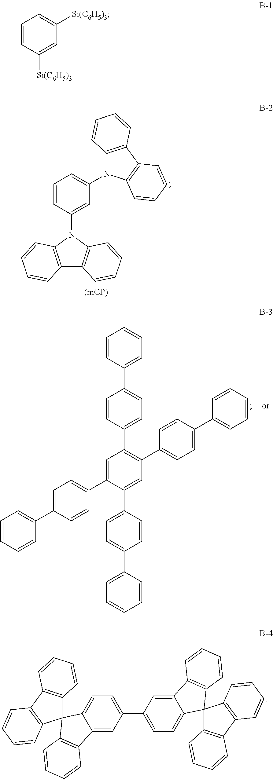
Suitable materials for use in the ETL1, having a LUMO level higher (less negative) than the LUMO level of the anthracene used in the ETL2 are derivatives of benzene and naphthalene as well as organometallic compounds of iridium. The difference between the LUMO levels of the material in the ETL1 and the anthracene in the ETL2 is indicative of the energy barrier for electron injection and provides the benefits of the invention. Preferably, the difference in LUMO levels should be at least 0.26 eV or, more preferably, it should exceed 0.35 eV.
The LUMO level (energy) for any compound can often be experimentally determined using well-known techniques (see, for examples, U.S. Pat. No. 7,132,174 B2, U.S. Pat. No. 7,128,982 B2, US Patent Publication 2006/0246315 or U.S. Pat. No. 7,045,952 B2) or can be calculated from theory. If possible, the HOMO (highest occupied molecular orbital) and LUMO (lowest unoccupied molecular orbital) energies of a compound should be experimentally determined for this invention. Experimentally determined LUMO energy data shown in the Table A for specific compounds were evaluated by the cyclic voltammetry method. Each LUMO energy was evaluated by adding 4.8 eV to the reduction potential vs. s.c.e. (saturated calomel electrode) using a solvent mixture of acetonitrile and toluene (50%/50% v/v, i.e., 1:1 acetonitrile/toluene by volume) containing 0.1M TBAF (tetrabutylammonium tetrafluoroborate) as the supporting electrolyte.
However, if the energies are unavailable or cannot be measured, theoretically calculated values can be used. HOMO and LUMO energies for a molecule can be derived from the orbital energies of Density Functional Theory calculations (here termed “raw” orbital energies). These raw HOMO and LUMO orbital energies (EHraw and ELraw respectively) are modified using an empirically derived linear correlation whose parameters were obtained previously by comparing the computed raw energies of various molecules to experimental energies obtained from electrochemical data. The HOMO and LUMO energies are given by this correlation according to equations 1 and 2:
HOMO=0.643*(E Hraw)−2.13  (eq. 1)
LUMO=0.827*(E Lraw)−1.09  (eq. 2)
EHraw is the raw energy of the HOMO, and ELraw is the raw energy of the LUMO, and all quantities are expressed in electron volts (eV). Values of EHraw and ELraw are obtained using the B3βYP method as implemented in the Gaussian 98 (Gaussian, Inc., Pittsburgh, Pa.) computer program. The basis set for use with the B3βYP method is defined as follows: MIDI! for all atoms for which MIDI! is defined, 6-31β* for all atoms defined in 6-31β* but not in MIDI!, and either the LACV3β or the LANL2βZ basis set and pseudopotential for atoms not defined in MIDI! or 6-31β*, with LACV3β being the preferred method. For any remaining atoms, any published basis set and pseudopotential can be used. MIDI!, 6-31β* and LANL2βZ are used as implemented in the Gaussian98 computer code and LACV3β is used as implemented in the Jaguar 4.1 (Schrodinger, Inc., Portland Oreg.) computer code. For polymeric or oligomeric materials, it is sufficient to compute EHraw and ELraw over a monomer or oligomer of sufficient size so that additional units do not substantially change the values of EHraw and ELraw. It should be noted that the calculated energy values can typically show some deviation from the experimental values. Because the molecular orbital energies cannot be either calculated or measured accurately in some situations, LUMO energies differing by less than 0.05 should be considered equal for the purposes of this invention. The calculated LUMO energies are also shown in Table A. The experimentally determined values generally agree well with the calculated numbers. As stated above, the LUMO values for the materials of the invention should be experimentally determined and calculated LUMO values should be used only when it is not possible to experimentally determine the LUMO values. In any case, experimental values should be compared only to other experimental values and calculated values compared only to calculated values.
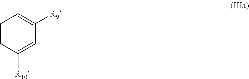
One class of suitable materials for the ETL1 is benzene derivatives according to Formula (III):
Figure US08242489-20120814-C00007

wherein at least two of R8-R11 both represent hydrogen or substituted carbon, silicon or nitrogen atoms with the proviso that no more than two of R8-R11 are hydrogen.
When at least two of R8-R11 in Formula (III) both represent substituted silicon or nitrogen atoms, then the preferred benzene derivatives are those where R8 and R11 are both hydrogen as shown in Formula (IIIa):
Figure US08242489-20120814-C00008

where R9′ and R10′ are both tri-substituted silicon atoms or both di-substituted nitrogen atoms. While R9′ and R10′ can be different, it is preferred that they are identical. Suitable examples of tri-substituted silicon atoms are triphenylsilyl, tri-t-butylsilyl and diphenylnaphthylsilyl. Suitable examples of di-substituted nitrogen atoms are diphenylamino, di(p-methylphenyl)amino, N-phenyl-N-1-naphthylamino and heterocycles like carbazolyl.
Some illustrative examples of compounds according to Formula (IIIa) are:
Figure US08242489-20120814-C00009
When at least two of R8-R11 in formula (III) both represent substituted carbon atoms, then the preferred benzene derivatives are those where R8-R10 are all substituted carbon atoms as shown in Formula (IIIb):
Figure US08242489-20120814-C00010

where R8*-R10* are tetrasubstituted or aromatic carbon atoms. In Formula (IIIb), R11* can be a hydrogen or a tetrasubstituted or aromatic carbon atom. Examples of suitable aromatic carbon atoms are carbon atoms belonging to substituted or unsubstituted phenyl, naphthyl, or fluorenyl ring systems.
Some illustrative examples of compounds according to Formula (IIIb) are:
Figure US08242489-20120814-C00011
Another class of suitable materials for the ETL1 is naphthalene derivatives. In order to have higher LUMO levels than anthracenes, useful naphthalene derivatives are those with no additional fused aromatic rings and whose substituents are attached to the core naphthyl nucleus via single bonds. Suitable naphthyl derivatives are according to Formula (IV):
Figure US08242489-20120814-C00012

wherein R12 is an aromatic substituent and p is 2 to 8. Suitable aromatic substituents are substituted or unsubstituted phenyl, naphthyl, carbazolyl, phenanthryl or aromatic heterocycles such as pyridine. Preferred are phenyl groups with p=4.
An illustrative example of a compound according to Formula (IV) is:
Figure US08242489-20120814-C00013
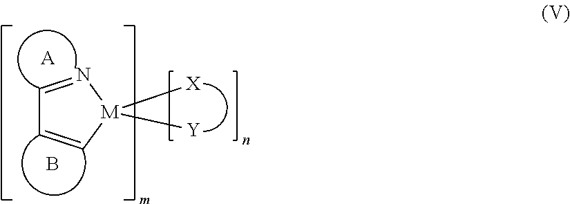
Yet another class of suitable materials for the ETL1 is cyclometallated organometallic complexes of iridium. Although such a compound is often used as a phosphorescent dopant in a LEL, in the present usage it should not emit any significant amount of light (less than 10% of the total amount of light from the device). When used as the single material in a layer in any OLED, such a compound generally emits weakly if at all, because of a phenomenon known as concentration quenching. Further, contact with an anthracene in the adjoining LEL or ETL2 favors energy transfer to the anthracene, tending to suppress any remaining emission. For iridium complexes that emit green or greater wavelength light, any emission from an ETL1 containing the iridium complex can easily be determined from examination of the EL light output. Suitable iridium complexes are according to Formula (V):
Figure US08242489-20120814-C00014

wherein:
M is iridium;
A is a substituted or unsubstituted heterocyclic ring containing at least one nitrogen atom;
B is a substituted or unsubstituted aromatic or heteroaromatic ring, or ring containing a vinyl or aromatic carbon bonded to M;
X—Y is an anionic bidentate ligand;
m is an integer from 1 to 3 and
n in an integer from 0 to 2 such that m+n=3.
Compounds according to Formula (V) can be referred to as C,N- (or C^N-) cyclometallated complexes to indicate that the central metal atom is contained in a cyclic unit formed by bonding the metal atom to carbon and nitrogen atoms of one or more ligands. Examples of heterocyclic ring A in formula (V) include substituted or unsubstituted pyridine, quinoline, isoquinoline, pyrimidine, indole, indazole, thiazole, and oxazole rings. Examples of ring B in Formula (V) include substituted or unsubstituted phenyl, napthyl, thienyl, benzothienyl, furanyl rings. Ring B in formula (V) can also be a N-containing ring such as pyridine, with the proviso that this N-containing ring bonds to M through a C atom as shown in formula (V), and not through a N atom.
An example of a tris-C,N-cyclometallated complex according to formula (V) with m=3 and n=0 is tris(2-phenyl-pyridinato-N,C2′-)iridium(III), (Ir(ppy)3) shown below in stereodiagrams as facial (fac-) or meridional (mer-) isomers.
Figure US08242489-20120814-C00015
Additional examples of tris-C,N-cyclometallated iridium complexes according to formula (IC) are tris(2-phenyl-4-t-butylpyridinato-N,C2)iridium(III) (Ir(tbuppy)3), tris(2-(4′-methylphenyl)pyridinato-N,C2′)iridium(III), tris(3-phenylisoquinolinato-N,C2′)iridium(III), tris(2-phenylquinolinato-N,C2′)iridium(III), tris(1-(4′-methylphenyl)isoquinolinato-N,C2′)iridium(III), tris(2-(4′,6′-difluorophenyl)-pyridinato-N,C2′)iridium(III), tris(2-((5′-phenyl)-phenyl)pyridinato-N,C2′)iridium(III), tris(2-(2′-benzothienyl)pyridinato-N,C3′)iridium(III), tris(2-phenyl-3,3′dimethylindolato-N,C2′)iridium(III), and tris(1-phenyl-1H-indazolato-N,C2′)iridium(III). Of these, Ir(ppy)3 and Ir(tbuppy)3 are particularly suitable for this invention
Suitable iridium complexes also include compounds according to formula (V) wherein the monoanionic bidentate ligand X—Y is another C,N-cyclometallating ligand. Examples include bis(1-phenylisoquinolinato-N,C2′)(2-phenylpyridinato-N,C2′)iridium(III) and bis(2-phenylpyridinato-N,C2′) (1-phenylisoquinolinato-N,C2′)iridium(III). Suitable iridium complexes according to Formula (V) can, in addition to the C,N-cyclometallating ligand(s), also contain monoanionic bidentate ligand(s) X—Y that are not C,N-cyclometallating. Common examples are beta-diketonates such as acetylacetonate, and Schiff bases such as picolinate. Examples of such mixed ligand complexes according to formula (V) include bis(2-phenylpyridinato-N,C2′)iridium(III)(acetylacetonate), bis(2-(2′-benzothienyl)pyridinato-N,C3′)iridium(III)(acetylacetonate), and bis(2-(4,6′-difluorophenyl)-pyridinato-N,C2′)iridium(III)(picolinate). It should be noted that iridium complexes that can be suitably used in the ETL1 should be selected according their LUMO levels from this broad list.
The devices of the invention contain an ETL2 which is located between the ETL1 and the cathode and which consists essentially of an anthracene. The function of this layer is to transport electrons. Ideally, this layer is located in direct contact to the cathode side of the ETL1. Suitable anthracenes for this usage are the same as those used as hosts in the LEL according to Formula (I). Although a mixture of anthracenes can be used, it is desirable for simplicity that a single anthracene is used. By “consists essentially of an anthracene”, it is meant that this layer is composed of anthracene derivatives except that it can contain small and insignificant amounts of other materials such as not to materially affect the basic electrical properties that would characterize the layer in their absence. Desirably, the ETL2 is composed of at least 99% of a single anthracene derivative.
As noted above, the total thickness of the (optional ETL3)/ETL1/ETL2 unit can be in the range of 1-50 nm, preferably between 5 and 30 nm, so that the thickness of the ETL2 should be no more than about 49.5 nm, and desirably less than about 29.5 nm.
In some embodiments of the invention, there is an additional electron-injection layer (EIL) or layers present between the ETL2 and the cathode. The function of an EIL is to facilitate the injection of electrons from the cathode to the ETL2. Examples of suitable materials for the electron-injection layer include, but are not limited to, phenanthrolines (such as 4,7-diphenyl-1,10-phenanthroline (Bphen)), organic alkali metal or alkaline earth salts (such as lithium 8-hydroxyquinolate (LiQ), tris(quinolin-8-olato)aluminum(III) (Alq) or its derivatives), inorganic salts (such as LiF) or combinations thereof. The electron-injection layer can also be doped with metals such as lithium.
In one suitable embodiment the EL device emits white light, in which case the device typically includes one or more emitters of complementary color(s). To produce a white emitting device, ideally the device would comprise a layer with a blue fluorescent emitter together with proper proportions of a yellow emitting layer, or a combination of green and red emitting layers, suitable to make white emission. This invention can be used in so-called stacked device architecture, for example, as taught in U.S. Pat. No. 5,703,436 and U.S. Pat. No. 6,337,492. Embodiments of the current invention can be used in stacked devices that comprise solely fluorescent elements to produce white light. The blue LEL of the invention is a fluorescent layer. The white device can also include combinations of fluorescent emitting materials and phosphorescent emitting materials (sometimes referred to as hybrid OLED devices). For example, white emission can be produced by one or more hybrid blue fluorescent/red phosphorescent elements stacked in series with a green phosphorescent element using p/n junction connectors as disclosed in Tang et al. U.S. Pat. No. 6,936,961 B2. White-emitting OLEDs may be used with suitable color filters to produce colored light for the pixels of a display device.
In one desirable embodiment, the EL device is part of a display device. In another suitable embodiment, the EL device is part of an area lighting device. The EL device of the invention is useful in any device where stable light emission is desired such as a lamp or a component in a static or motion imaging device, such as a television, cell phone, DVD player, or computer monitor.
As used herein and throughout this application, chemical terms are generally as defined by the Grant & Hackh's Chemical Dictionary, Fifth Edition, McGraw-Hill Book Company. For the purpose of this invention, also included in the definition of a heterocyclic ring are those rings that include coordinate bonds. The definition of a coordinate or dative bond can be found in Grant & Hackh's Chemical Dictionary, pages 91 and 153. The definition of a ligand, including a multidentate ligand, can be found in Grant & Hackh's Chemical Dictionary, pages 337 and 176, respectively. Unless otherwise specifically stated, use of the term “substituted” or “substituent” refers to any group or atom other than hydrogen. Additionally, when the term “group” is used, it means that when a substituent group contains substitutable hydrogen, it is also intended to encompass not only the substituent's unsubstituted form, but also its form further substituted with any substituent group or groups as herein mentioned, so long as the substituent does not destroy properties necessary for device utility. If desired, the substituents can themselves be further substituted one or more times with the described substituent groups. The particular substituents used can be selected by those skilled in the art to attain desirable properties for a specific application and can include, for example, electron-withdrawing groups, electron-donating groups, and groups providing steric bulk. When a molecule can have two or more substituents, the substituents can be joined together to form a ring such as a fused ring unless otherwise provided.
Basic OLED information and description of the layer structure, material selection, and fabrication process for OLED devices.can be found in the following along with the references cited therein: Chen, Shi, and Tang, “Recent Developments in Molecular Organic Electroluminescent Materials,” Macromol. Symp. 125, 1 (1997); Hung and Chen, “Recent Progress of Molecular Organic Electroluminescent Materials and Devices,” Mat. Sci. and Eng. R39, 143 (2002); H. Yersin, “Highly Efficient OLEDS with Phosphorescent Materials” (Wiley-VCH (Weinheim), 2007); K. Mullen and U. Scherf, “Organic Light Emitting Devices: Synthesis, Properties and Applications” (Wiley-VCH (Weinheim), 2006); J. Kalinowski, “Organic Light-Emitting Diodes: Principles, Characteristics and Processes (Optical Engineering)” (Dekker (NY), 2004); Z. Li and H. Meng, “Organic Light-Emitting Materials and Devices (Optical Science and Engineering)” (CRC/Taylor & Francis (Boca Raton), 2007) and J. Shinar, “Organic Light-Emitting Devices” (Springer (NY), 2002).
The present invention can be employed in many OLED configurations using small molecule materials, oligomeric materials, polymeric materials, or combinations thereof. These include from very simple structures having a single anode and cathode to more complex devices, such as passive matrix displays having orthogonal arrays of anodes and cathodes to form pixels, and active-matrix displays where each pixel is controlled independently, for example, with thin film transistors (TFTs). There are numerous configurations of the organic layers wherein the present invention is successfully practiced. For this invention, essential requirements are a cathode, an anode, a LEL and two ETLs.
One embodiment according to the present invention and especially useful for a small molecule device is shown in FIG. 1. OLED 100 contains a substrate 110, an anode 120, a hole-injecting layer 130, a hole-transporting layer 132, a light-emitting layer (LEL) 134, a thin first electron-transporting layer (ETL1) 135, a second electron-transporting layer (ETL2) 136, an electron-injecting layer (EIL) 138 and a cathode 140. The LEL 134 contains the inventive combination of anthracene host and styrylamine dopant, with thin layer 135 representing the inventive ETL1 with the material that has a less negative LUMO level than the anthracene in the ETL2, and ETL 136 representing the ETL2. Note that the substrate 110 can alternatively be located adjacent to the cathode 140, or the substrate can actually constitute the anode 120 or cathode 140. Also, the total combined thickness of the organic layers is preferably less than 500 nm.
In other embodiments, the EIL (138) can be subdivided into two or more sublayers, namely a first electron-injecting layer (EIL1) adjacent to the ETL2 (136) and a second electron-injecting layer (ETL2) located between the EIL1 and the cathode. In yet another embodiment, the HIL (130) can be subdivided into two or more sublayers, namely a first hole-injecting layer (HIL1) between the anode and the HTL, and a second hole-injecting layer (HIL2) between the HIL1 and the anode.
The anode 120 and cathode 140 of the OLED are connected to a voltage/current source 150, through electrical conductors 160. Applying an electrical potential difference between the anode 120 and cathode 140 such that the anode is at a more positive potential than the cathode operates the OLED. Holes are injected into the organic light-emitting structure from the anode 120. Electrons are injected from the cathode 140. Enhanced device stability can sometimes be achieved when the OLED is operated in an AC mode where, for some time period in a cycle, the potential bias is reversed and no current flows. An example of an AC driven OLED is described in U.S. Pat. No. 5,552,678.
For full color display, the pixelation of LELs can be needed. This pixelated deposition of LELs is achieved using shadow masks, integral shadow masks, U.S. Pat. No. 5,294,870, spatially defined thermal dye transfer from a donor sheet, U.S. Pat. Nos. 5,688,551, 5,851,709, and 6,066,357 and an inkjet method, U.S. Pat. No. 6,066,357.
OLEDs of this invention can employ various well-known optical effects in order to enhance their emissive properties if desired. These include optimizing layer thicknesses to yield improved light extraction, providing dielectric mirror structures, replacing reflective electrodes with light-absorbing electrodes, providing anti-glare or anti-reflection coatings over the display, providing a polarizing medium over the display, or providing colored, neutral density, or color-conversion filters over the display. Filters, polarizers, and anti-glare or anti-reflection coatings can be specifically provided over the OLED or as part of the OLED.
Embodiments of the invention can provide EL devices that have good luminance efficiency, good operational stability, excellent color and low drive voltages. Embodiments of the invention can be produced consistently and with high reproducibility to provide good power efficiency. They can have lower power consumption requirements and, when used with a battery, provide longer battery lifetimes.
The invention and its advantages are further illustrated by the specific examples that follow. The term “percentage” or “percent” and the symbol “%”, applied to mixtures of materials, indicates the volume percent (or a thickness ratio as measured on a thin film thickness monitor) of a particular first or second compound relative to the total material in a layer of the invention. If more than one second compound is present, the total volume of the second compounds can also be expressed as a percentage of the total material in the layer of the invention.
EXPERIMENTAL EXAMPLES
The following table lists LUMO values for selected materials used in the following experiments. TPBI is 2,2′,2″-(1,3,5-benzenetriyl)tris[1-phenyl-1H-benzimidazole]. Alq is tris(quinolin-8-olato)aluminum(III). BAlq′ is bis(2-methylquinolin-8-olato)(2,6-diphenyl-phenolato)aluminum(III). CH-1 is bis(9,9′-spirobifluorene-2-yl) ketone.
TABLE A
Experimentally-determined (column 2) and calculated
(column 3) LUMO energies for selected materials.
Material LUMO exp LUMO calc
A-1 −2.52 −2.53
A-2 −2.44 −2.46
A-3 −2.45 −2.45
A-4 −2.45 −2.46
A-5 −2.40 −2.40
CBP −1.96 −2.13
CH-1 −2.42 −2.50
Alq −2.50 −2.51
N-1 −1.95 −2.03
B-1 −1.60
B-2 (mCP) −1.78 −1.75
NPB −1.93 −2.06
B-3 −2.21
B-4 −2.13 −2.13
Ir(ppy)3 −2.04 −2.10
Bphen −2.40 −2.29
TPBI −2.27 −2.09
BAlq′ −2.42 −2.50
F-1 −2.57 −2.61
Example Series 1
EL devices 1-1 to 1-36 were constructed in the following manner:
  • 1. A glass substrate, coated with an approximately 25 nm layer of indium-tin oxide (ITO) as the anode, was sequentially ultrasonicated in a commercial detergent, rinsed in deionized water, dried and exposed to oxygen plasma for about 1 minute.
  • 2. Over the ITO a 1 nm fluorocarbon (CFx) hole injecting layer (HIL1) was deposited by plasma-assisted deposition of CHF3 as described in U.S. Pat. No. 6,208,075.
  • 3. A 10 nm layer of dipyrazino[2,3-f:2′,3′-h]quinoxaline-2,3,6,7,10,11-hexacarbonitrile (HAT-CN) was then vacuum-deposited as a second hole-injection layer (HIL2).
  • 4. Next, a hole transporting layer (HTL) of N,N′-di-1-naphthyl-N,N′-diphenyl-4,4′-diaminobiphenyl (NPB) was vacuum-deposited to a thickness of 75 nm.
  • 5. A 25 nm light emitting layer including A-4 and 7% S-2 was then vacuum-deposited onto the HTL.
  • 6. A thin first ETL (ETL1) was vacuum-deposited over the LEL with thickness and composition according to Table 1.
  • 7. A second electron transporting layer (ETL2) of A-1 was vacuum-deposited over the ETL1. The thickness was adjusted so that the thickness of the ETL1 and the ETL2 together was always 20 nm.
  • 8. A 10 nm thick electron injecting layer (EIL) of 4,7-diphenyl-1,10-phenanthroline (Bphen) was then vacuum-deposited over the ETL2. In Examples 1-28 to 1-33, this layer was additionally doped with 1.2% lithium.
  • 9. Lithium fluoride (0.5 nm) was then vacuum-deposited over the EIL, followed by a 100 nm layer of aluminum, to form a bilayer cathode. In Examples 1-28 to 1-33, the LiF layer was omitted.
The above sequence completed the deposition of the EL device. The device, together with a desiccant, was then hermetically packaged in a dry glove box for protection against the ambient environment. The cells thus formed were tested for efficiency and color at an operating current density of 20 mA/cm2 and the results are reported in the form of driving voltage (V), luminous yield (cd/A), external quantum efficiency (EQE), and 1931 CIE (Commission Internationale de l'Eclairage) coordinates. EQE is given as a percentage and is the ratio of photons of light that are emitted externally from the device to the number of electrons (or holes) injected into the OLED device. It was evaluated by measuring the EL emission perpendicular to the plane of the device and assuming that emission in other directions has a Lambertian distribution. The anthracene host is A-4 in all devices of series 1.
TABLE 1
Variation of the Thin First Electron Transporting Layer (ETL1) using
an Anthracene as the Second Electron Transporting Layer (ETL2)
ETL1
Thick-
ness
Example ETL2 ETL1 (nm) V cd/A CIEx CIEy EQE
1-1 A-1 None None 3.2 8.3 0.141 0.163 6.5
(Comp)
1-2 A-1 N-1 0.5 3.1 8.20 0.141 0.163 6.4
(Comp)
1-3 A-1 N-1 1.5 3.3 10.3 0.141 0.162 8.0
(Inv)
1-4 A-1 N-1 2.5 3.5 12.2 0.141 0.166 9.4
(Inv)
1-5 A-1 N-1 3.5 3.7 10.4 0.141 0.161 8.1
(Inv)
1-6 A-1 N-1 5.0 4.5 7.7 0.141 0.160 6.0
(Comp)
1-7 A-1 B-1 1.0 3.4 12.7 0.141 0.182 9.2
(Inv)
1-8 A-1 B-1 1.5 3.4 10.2 0.141 0.182 9.4
(Inv)
1-9 A-1 B-1 2.5 4.0 11.2 0.141 0.183 8.1
(Inv)
1-10 A-1 mCP 1.5 3.3 11.9 0.141 0.183 8.6
(Inv)
1-11 A-1 mCp 2.5 3.4 12.4 0.141 0.180 9.1
(Inv)
1-12 A-1 mCp 3.5 3.4 12.6 0.141 0.179 9.2
(Inv)
1-13 A-1 NPB 1.5 3.3 10.4 0.141 0.159 8.2
(Inv)
1-14 A-1 B-3 1.5 3.2 11.0 0.142 0.165 8.5
(Inv)
1-15 A-1 B-3 2.5 3.3 11.8 0.141 0.163 9.2
(Inv)
1-16 A-1 B-3 3.5 3.4 11.4 0.141 0.163 8.9
(Inv)
1-17 A-1 B-3 5.0 3.9 10.1 0.141 0.163 7.8
(Comp)
1-18 A-1 B-4 0.5 3.1 8.8 0.141 0.177 6.4
(Comp)
1-19 A-1 B-4 1.5 3.4 11.4 0.141 0.176 8.4
(Inv)
1-20 A-1 B-4 2.5 3.6 11.0 0.141 0.177 8.1
(Inv)
1-21 A-1 B-4 5.0 4.6 7.3 0.141 0.170 5.5
(Comp)
1-22 A-1 Ir(ppy)3 1.5 3.3 10.2 0.141 0.176 7.5
(Inv)
1-23 A-1 Ir(ppy)3 2.5 3.4 11.2 0.141 0.178 8.2
(Inv)
1-24 A-1 Ir(ppy)3 3.5 3.5 10.6 0.141 0.180 7.7
(Inv)
1-25 A-1 Ir(ppy)3 5.0 3.8 9.5 0.141 0.171 7.0
(Comp)
1-26 A-1 N-1 + 2.5 3.5 12.0 0.141 0.178 8.8
(Inv) 2% A-4
1-27 A-1 N-1 + 2.5 3.4 11.8 0.141 0.180 8.6
(Inv) 10% A-4
1-28 A-1 None -None 3.3 9.9 0.141 0.178 7.3
(Comp)
1-29 A-1 N-1 2.5 3.5 11.3 0.141 0.175 8.3
(Inv)
1-30 A-1 N-1 3.5 3.7 10.8 0.141 0.173 8.1
(Inv)
1-31 A-1 N-1 5.0 4.1 8.86 0.141 0.174 6.6
(Comp)
1-32 A-1 mCP 2.5 3.4 11.8 0.141 0.175 8.7
(Inv)
1-33 A-1 mCP 5.0 4.2 8.7 0.141 0.175 6.5
(Comp)
1-34 A-1 TPBI 2.5 3.9 8.7 0.141 0.178 6.4
(Comp)
1-35 A-1 TPBI 5.0 4.3 7.8 0.141 0.178 5.7
(Comp)
1-36 A-1 TPBI 7.5 4.3 7.5 0.141 0.181 5.5
(Comp)
In Table 1, comparison of inventive examples 1-3 to 1-5 with comparative examples 1-2 or 1-6, all with a material with a less negative LUMO level compared to the anthracene in the ETL2, shows that the ETL1 adjacent to the LEL should have a thickness range of greater than 0.5 nm but less than 5.0 nm in order to show high efficiency and low drive voltage. Examples 1-7 to 1-27 show that the same improvement in efficiency occurs with other classes of materials with a less negative LUMO level than the anthracene of the ETL2 in the same thickness range. Inventive examples 1-26 and 1-27 demonstrate that the ETL1 can be doped with a small amount of an anthracene and maintain high efficiency. Examples 1-29, 1-30, and 1-32 show that further doping the EIL with metallic lithium, while omitting the LiF, retains the high efficiency.
For comparative Examples 1-34 to 1-36, the results show that use of TPBI in the thin first ETL adversely affects device performance. The LUMO energy of TPBI is less negative than the LUMO energy of anthracene A-1 used in the ETL2 as shown in Table A. Thus, the bather is created for electron injection from the ETL2 into a layer of TPBI. For experimentally determined LUMO levels this barrier is 0.25 eV, which is too small to provide the improved device performance. It is desirable for achievement of the inventive efficiency improvement that the difference in LUMO levels of materials used in the ETL1 and the ETL2 be greater than 0.35 eV.
Example Series 2
EL devices 2-1 to 2-9 were constructed in the same manner as Example Series 1 except that the material in the LEL was varied according to Table 2. CBP is 4,4′-bis(N-carbazolyl)-1,1′-biphenyl. Devices were aged electrically at room temperature at a constant current density of 80 mA/cm2 (DC mode). The lifetime (T50), or operational stability, of an OLED device is defined as the number of hours required for the luminance at 80 mA/cm2 to drop to half the luminance of the fresh device.
TABLE 2
ETL1 Variations with Anthracene and Non-Anthracene
LEL Host and Anthracene A-1 in ETL2
ETL1
LEL Thickness T50 at 80
Example host ETL1 (nm) V cd/A EQE mA/cm2
1-1 A-1 None None 3.2 8.3 6.5 165
(Comp)
1-2 A-1 N-1 0.5 3.1 8.20 6.4 175
(Comp)
1-3 A-1 N-1 1.5 3.3 10.3 8.0 147
(Inv)
1-4 A-1 N-1 2.5 3.5 12.2 9.4 111
(Inv)
1-5 A-1 N-1 3.5 3.7 10.4 8.1 74
(Inv)
1-6 A-1 N-1 5.0 4.5 7.7 6.0 102
(Comp)
1-10 A-1 mCp 1.5 3.3 11.9 8.6 162
(Inv)
1-11 A-1 mCp 2.5 3.4 12.4 9.1 168
(Inv)
1-12 A-1 mCp 3.5 3.4 12.6 9.2 125
(Inv)
2-1 CBP None None 5.0 3.5 2.7 27
(Comp)
2-2 CBP N-1 1.5 4.9 4.7 3.4 24
(Comp)
2-3 CBP N-1 2.5 5.2 4.9 3.6 18
(Comp)
2-4 CBP N-1 3.5 5.4 4.6 3.4 16
(Comp)
2-5 CBP N-1 5.0 5.8 4.1 3.0 23
(Comp)
2-6 CBP mCp 1.5 5.2 4.2 3.1 25
(Comp)
2-7 CBP mCp 2.5 5.3 3.8 2.8 20
(Comp)
2-8 CBP mCp 3.5 5.5 3.1 2.3 12
(Comp)
2-9 CBP mCp 5.0 5.9 2.0 1.6 12
(Comp)
In Table 2, comparative examples 2-1 to 2-9 demonstrate that using a host that is not an anthracene in the LEL with a blue styrylamine emitter causes low efficiency and significantly degrades stability. The efficiency can be improved to a small degree by the addition of an ETL1 according to the invention but overall external quantum efficiency remains much less than that of the blue fluorescent devices with an anthracene in the LEL.
Example Series 3
EL devices 3-1 to 3-27 were constructed in the same manner as Example Series 1 except that the material in the ETL2 was varied according to Table 3. In examples 3-11 to 3-27, the thickness was adjusted so that the thickness of the ETL1 and ETL2 together was always 30 nm and the EIL of Bphen of step 8 was omitted. F-1 and BAlq′ have the following structures:
Figure US08242489-20120814-C00016
TABLE 3
ETL1 Variations with Anthracene
LEL Host and Non-Anthracene ETL2
ETL1
Thick-
ness
Example ETL1 (nm) ETL2 V cd/A CIEx CIEy EQE
3-1 None None F-1 3.4 9.6 0.141 0.169 7.2
(Comp)
3-2 N-1 0.5 F-1 3.5 10.2 0.141 0.169 7.8
(Comp)
3-3 N-1 1.5 F-1 3.6 10.2 0.141 0.167 7.8
(Comp)
3-4 N-1 2.5 F-1 3.8 9.4 0.141 0.167 7.2
(Comp)
3-5 N-1 3.5 F-1 4.1 8.2 0.141 0.166 6.3
(Comp)
3-6 N-1 5.0 F-1 4.6 6.9 0.141 0.165 5.3
(Comp)
3-7 None None A-1 + 4.5 5.8 0.141 0.176 4.3
(Comp) Bphen
(1:1)
3-8 mCp 1.5 A-1 + 4.4 5.6 0.141 0.167 4.3
(Comp) Bphen
(1:1)
3-9 mCp 2.5 A-1 + 4.5 5.3 0.141 0.166 4.0
(Comp) Bphen
(1:1)
3-10 mCp 5.0 A-1 + 4.9 4.4 0.141 0.163 3.4
(Comp) Bphen
(1:1)
3-11 None None Alq 5.9 7.3 0.144 0.190 5.1
(Comp)
3-12 N-1 2.5 Alq 6.1 7.0 0.143 0.190 5.0
(Comp)
3-13 N-1 5.0 Alq 6.7 6.2 0.142 0.178 4.5
(Comp)
3-14 None None Alq 5.9 7.7 0.144 0.192 5.3
(Comp)
3-15 mCp 0.5 Alq 5.8 7.0 0.144 0.195 4.8
(Comp)
3-16 mCp 1.5 Alq 6.1 7.2 0.144 0.194 4.9
(Comp)
3-17 mCp 2.5 Alq 6.2 6.9 0.144 0.191 4.8
(Comp)
3-18 mCp 5.0 Alq 7.1 4.7 0.150 0.206 3.0
(Comp)
3-19 mCp 7.5 Alq 8.2 2.0 0.205 0.334 0.9
(Comp)
3-20 None None BAlq′ 9.9 4.2 0.141 0.170 3.2
(Comp)
3-21 mCp 0.5 BAlq′ 10.0 4.0 0.141 0.171 3.0
(Comp)
3-22 mCp 1.5 BAlq′ 10.1 3.4 0.141 0.171 2.6
(Comp)
3-23 mCp 2.5 BAlq′ 9.9 3.2 0.141 0.170 2.4
(Comp)
3-24 mCp 5.0 BAlq′ 10.1 2.3 0.142 0.173 1.7
(Comp)
3-25 mCp 7.5 BAlq′ 10.3 1.8 0.143 0.178 1.3
(Comp)
3-26 None None TPBI 6.1 7.3 0.141 0.178 5.4
(Comp)
3-27 mCp 5.0 TPBI 6.9 5.7 0.141 0.170 4.3
(Comp)
The results in Table 3 confirm that when the ETL2 is not an anthracene or even if the anthracene is mixed with a significant amount of another non-anthracene material, there is little or no increase in efficiency, or even a decrease in efficiency when a thin layer (ETL1) of a less negative LUMO material is placed between the LEL and the ETL2.
Example Series 4
EL devices 4-1 to 4-20 were constructed in the same manner as Example Series 1 except that the light-emitting material in the LEL was according to Table 4. The LEL host is A-4 and ETL2 is A-1. The comparative emitters have the following structures:
Figure US08242489-20120814-C00017
TABLE 4
LEL Emitter Variations
ETL1
Thick-
ness
Example ETL1 (nm) LEL V cd/A CIEx CIEy EQE
4-1 None None   6% 3.6 28.5 0.274 0.654 7.8
(Comp) CE-1
4-2 N-1 1.5   6% 3.6 28.1 0.275 0.654 7.7
(Comp) CE-1
4-3 N-1 2.5   6% 3.8 31.4 0.272 0.657 8.6
(Comp) CE-1
4-4 N-1 3.5   6% 4.4 29.9 0.272 0.657 8.1
(Comp) CE-1
4-5 N-1 5.0   6% 5.8 23.7 0.271 0.657 6.5
(Comp) CE-1
4-6 None None   1% 3.2 6.9 0.132 0.195 4.9
(Comp) CE-2
4-7 N-1 0.5   1% 3.3 6.6 0.132 0.194 4.7
(Comp) CE-2
4-8 N-1 1.5   1% 3.4 7.3 0.132 0.194 5.2
(Comp) CE-2
4-9 N-1 2.5   1% 3.6 7.3 0.132 0.195 5.2
(Comp) CE-2
4-10 N-1 3.5   1% 5.1 4.1 0.132 0.186 3.0
(Comp) CE-2
4-11 N-1 5.0   1% 5.1 4.1 0.132 0.186 5.0
(Comp) CE-2
4-12 None None 1.5% 5.9 3.5 0.139 0.121 5.7
(Comp) CE-3
4-13 CBP 1.5 1.5% 5.7 3.7 0.140 0.116 5.7
(Comp) CE-3
4-14 CBP 2.5 1.5% 6.1 3.7 0.138 0.117 6.1
(Comp) CE-3
4-15 CBP 3.5 1.5% 6.0 3.8 0.138 0.114 6.1
(Comp) CE-3
4-16 CBP 5.0 1.5% 5.5 4.0 0.139 0.112 5.7
(Comp) CE-3
4-17 NPB 1.5 1.5% 6.1 3.8 0.139 0.119 6.0
(Comp) CE-3
4-18 NPB 2.5 1.5% 5.3 4.2 0.138 0.115 5.4
(Comp) CE-3
4-19 NPB 3.5 1.5% 3.1 5.4 0.138 0.111 3.2
(Comp) CE-3
4-20 NPB 5.0 1.5% 0.8 7.2 0.139 0.107 0.9
(Comp) CE-3
The results in Table 4 confirm that when the emitter in the LEL is not a styrylamine, the addition of a thin electron-transporting layer with a less negative LUMO than the anthracene in the second ETL provides little or no improvement in efficiency.
Example Series 5
EL devices 5-1 to 5-6 were constructed in the following manner:
  • 1. A glass substrate, coated with an approximately 25 nm layer of indium-tin oxide (ITO) as the anode, was sequentially ultrasonicated in a commercial detergent, rinsed in deionized water, dried and exposed to an oxygen plasma for about 1 minute.
  • 2. Over the ITO a 1 nm fluorocarbon (CFx) hole injecting layer (HIL2) was deposited by plasma-assisted polymerization of CHF3 as described in U.S. Pat. No. 6,208,075.
  • 3. A 10 nm layer of dipyrazino[2,3-f:2′,3′-h]quinoxaline-2,3,6,7,10,11-hexacarbonitrile (HAT-CN) was then vacuum-deposited as a first hole-injection layer (HIL1).
  • 4. Next, a hole transporting layer (HTL) of N,N′-di-1-naphthyl-N,N′-diphenyl-4,4′-diaminobiphenyl (NPB) was vacuum-deposited to a thickness of 75 nm.
  • 5. A 25 nm light emitting layer including A-4 as host and 7% S-1 was then vacuum-deposited onto the HTL.
  • 6. An additional 10 nm anthracene layer of A-1 (ETL3) was vacuum-deposited over the LEL.
  • 7. A thin first ETL (ETL1) was vacuum-deposited over the LEL with thickness and composition according to Table 5.
  • 8. A second electron transporting layer (ETL2) of A-1 was vacuum-deposited over the ETL1. The thickness was adjusted so that the thickness of the ETL1 and ETL2 together was always 10 nm.
  • 9. A 10 nm thick electron injecting layer (EIL) of 4,7-diphenyl-1,10-phenanthroline (Bphen) was then vacuum-deposited over the ETL2.
  • 10. Lithium fluoride (0.5 nm) was then vacuum-deposited over the EIL, followed by a 100 nm layer of aluminum, to form a bilayer cathode
The above sequence completed the deposition of the EL device. The device, together with a desiccant, was then hermetically packaged in a dry glove box for protection against the ambient environment. The cells thus formed were tested as describes for Example series 1.
TABLE 5
Additional Anthracene Layer between the LEL and the ETL1
ETL1
Thickness
Example ETL1 (nm) V cd/A CIEx CIEy EQE
5-1 None none 3.2 9.3 0.141 0.171 7.0
(Comp)
5-2 CBP 2.5 3.3 10.4 0.141 0.167 7.9
(Inv)
5-3 NPB 1.5 3.2 10.3 0.141 0.168 7.9
(Inv)
5-4 N-1 2.5 3.6 11.2 0.141 0.175 8.3
(Inv)
5-5 N-1 + 5% 2.5 3.5 10.9 0.141 0.176 8.0
(Inv) A-1
5-6 N-1 + 10% 2.5 3.4 10.7 0.141 0.175 8.0
(Inv) A-1
The results in Table 5 confirm that the ETL1 need not be directly adjacent to the LEL to provide increased efficiency but can be separated from it by another layer (ETL3) which consists essentially of an anthracene. Examples 5-5 and 5-6 show that the ETL1, placed at a distance from the LEL as described above, can be doped with an anthracene and still provide the improvement in device efficiency.
Example Series 6
EL devices 6-1 to 6-8 were constructed in the following manner:
  • 1. A glass substrate, coated with an approximately 25 nm layer of indium-tin oxide (ITO) as the anode, was sequentially ultrasonicated in a commercial detergent, rinsed in deionized water, dried and exposed to an oxygen plasma for about 1 minute.
  • 2. Over the ITO a 1 nm fluorocarbon (CFx) hole injecting layer (HIL2) was deposited by plasma-assisted polymerization of CHF3 as described in U.S. Pat. No. 6,208,075.
  • 3. A 10 nm layer of dipyrazino[2,3-f:2′,3′-h]quinoxaline-2,3,6,7,10,11-hexacarbonitrile (HAT-CN) was then vacuum-deposited as a first hole-injection layer (HIL1).
  • 4. Next, a hole transporting layer (HTL) of N,N′-di-1-naphthyl-N,N′-diphenyl-4,4′-diaminobiphenyl (NPB) was vacuum-deposited to a thickness of 105 nm.
  • 5. In examples 6-1 to 6-5, a 35 nm light emitting layer (LEL) including BAlq′ as host and 8% tris(1-phenylisoquinolinato-N,C2′)iridium(III) (Ir(1-piq)3) as a phosphorescent emitter was then vacuum-deposited onto the HTL. In examples 6-6 to 6-8, the LEL consisted of a mixture of CH-1 host, 25% NPB as cohost, and 6% Ir(1-piq)3.
  • 6. A thin first ETL (ETL1) was vacuum-deposited over the LEL with thickness and composition according to Table 6.
  • 7. An electron transporting layer (ETL2) of A-1 was vacuum-deposited over the ETL1. The thickness was adjusted so the thickness of the ETL1 and ETL2 together was always 40 nm.
  • 8. A 10 nm thick electron injecting layer (EIL) of Bphen was then vacuum-deposited over the ETL2.
  • 9. Lithium fluoride (0.5 nm) was then vacuum-deposited over the EIL, followed by a 100 nm layer of aluminum, to form a bilayer cathode.
The above sequence completed the deposition of the EL device. The device, together with a desiccant, was then hermetically packaged in a dry glove box for protection against the ambient environment. The cells thus formed were tested for efficiency and color at an operating current density of 1 mA/cm2. Devices were aged electrically at room temperature at current density of 40 mA/cm2 in DC mode. The lifetime (T50), or operational stability, of these OLED devices is defined as the number of hours required for the luminance at 40 mA/cm2 to drop to half the luminance of the fresh device.
The structure of CH-1 is:
Figure US08242489-20120814-C00018
TABLE 6a
Phosphorescent LEL Evaluation
ETL1
Thickness
Example ETL1 (nm) V cd/A CIEx CIEy EQE
6-1 None None 3.6 10.5 0.68 0.32 13.6
(Comp)
6-2 N-1 1.5 3.8 10.6 0.68 0.32 13.9
(Comp)
6-3 N-1 2.5 4.0 10.6 0.68 0.32 13.8
(Comp)
6-4 N-1 3.5 4.6 9.8 0.68 0.32 12.7
(Comp)
6-5 N-1 5.0 5.9 8.5 0.68 0.32 11.0
(Comp)
6-6 None None 2.6 10.3 0.68 0.32 12.9
(Comp)
6-7 N-1 1.5 2.6 10.8 0.68 0.32 13.7
(Comp)
6-8 N-1 3.5 2.8 11.2 0.68 0.32 14.1
(Comp)
TABLE 6b
Phosphorescent LEL Stability
ETL1 T50 at 40
Example ETL1 Thickness (nm) mA/cm2
6-1 (Comp) None None 721
6-2 (Comp) N-1 1.5 390
6-3 (Comp) N-1 2.5 123
6-4 (Comp) N-1 3.5 194
6-5 (Comp) N-1 5.0 n.a.
6-6 (Comp) None None 1202 
6-7 (Comp) N-1 1.5 942
6-8 (Comp) N-1 3.5 868
The results in Tables 6β and 6β indicate that the addition of an ETL1 to an OLED with a phosphorescent LEL provides little or no increase in efficiency even if the ETL1 has a material with a less negative LUMO than the material of the ETL2. Moreover, adverse effects on device stability are observed.
The invention has been described in detail with particular reference to certain preferred embodiments thereof, but it will be understood that variations and modifications can be effected within the spirit and scope of the invention.
PARTS LIST
100 OLED
110 Substrate
120 Anode
130 Hole-Injecting layer (HIL)
132 Hole-Transporting layer (HTL)
134 Light-Emitting layer (LEL)
135 Thin First Electron-Transporting Layer (ETL1)
136 Second Electron-Transporting layer (ETL2)
138 Electron-Injecting layer (EIL)
140 Cathode
150 Voltage/Current Source
160 Electrical Connectors

Claims (17)

1. An OLED device comprising:
an anode;
a cathode;
a light-emitting layer located therebetween, said light-emitting layer comprising an anthracene host and a styrylamine blue light-emitting compound; and
located between the said light-emitting layer and the cathode, a first electron-transporting layer that is greater than 0.5 nm and less than 5 nm thick and a second electron-transporting layer consisting essentially of an anthracene located between the first electron-transporting layer and the cathode;
wherein the first electron-transporting layer includes a compound with a less negative LUMO value than the anthracene in the second electron-transporting layer.
2. The OLED device of claim 1 wherein the difference in LUMO value between the compound in the first electron-transporting layer and the anthracene in the second electron-transporting layer is at least 0.26 eV.
3. The OLED device of claim 1 wherein the difference in LUMO value between the compound in the first electron-transporting layer and the anthracene in the second electron-transporting layer exceeds 0.35 eV.
4. The OLED device of claim 1 wherein the first electron-transporting layer is located in direct contact with the light-emitting layer.
5. The OLED device of claim 1 wherein the first electron-transporting layer additionally contains an anthracene.
6. The OLED device of claim 1 wherein there is an additional layer consisting essentially of an anthracene located between the first electron-transporting layer and the light-emitting layer.
7. The OLED device of claim 1 wherein the compound in the first electron-transporting layer is selected from benzene derivatives according to Formula (III):
Figure US08242489-20120814-C00019
wherein:
at least two of R8-R11 both represent hydrogen or substituted carbon, silicon or nitrogen atoms with the proviso that no more than two of R8-R11 are hydrogen.
8. The OLED device of claim 7 wherein the benzene derivative is selected from the group consisting of
Figure US08242489-20120814-C00020
9. The OLED device of claim 1 wherein the compound in the first electron-transporting layer is a naphthalene derivative according to Formula (IV)
Figure US08242489-20120814-C00021
wherein:
R12 is an aromatic substituent and p is 2 to 8.
10. The OLED device of claim 9 wherein the naphthalene derivative is:
Figure US08242489-20120814-C00022
11. The OLED device of claim 1 wherein the compound in the first electron-transporting layer is an iridium derivative according to Formula (V):
Figure US08242489-20120814-C00023
wherein:
M is iridium;
A is a substituted or unsubstituted heterocyclic ring containing at least one nitrogen atom;
B is a substituted or unsubstituted aromatic or heteroaromatic ring, or ring containing a vinyl or aromatic carbon bonded to M;
X-Y is an anionic bidentate ligand; m is an integer from 1 to 3 and
n in an integer from 0 to 2 such that m+n=3.
12. The OLED device of claim 11 wherein the iridium derivative is tris(2-phenyl-pyridinato-N,C2-)iridium (III).
13. The OLED device of claim 1 wherein the anthracene in the second electron-transporting layer is according to formula (I):
Figure US08242489-20120814-C00024
wherein:
R1 and R6 each independently represent an aryl group having 6-24 carbon atoms; R2-R5 and R7-R10 are each independently chosen from hydrogen, alkyl groups from 1-24 carbon atoms, or aromatic groups from 5-24 carbon atoms.
14. The OLED device of claim 6 wherein the anthracene in the additional layer is according to formula (I):
Figure US08242489-20120814-C00025
wherein:
R1 and R6 each independently represent an aryl group having 6-24 carbon atoms; R2-R5 and R7-R10 are each independently chosen from hydrogen, alkyl groups from 1-24 carbon atoms, or aromatic groups from 5-24 carbon atoms.
15. The OLED device of claim 14 wherein the anthracenes in both the second electron-transporting layer and the additional layer are the same.
16. The OLED device of claim 1 wherein the anthracene host in the light-emitting layer is according to Formula (I):
Figure US08242489-20120814-C00026
wherein:
R1 and R6 each independently represent an aryl group having 6-24 carbon atoms; R2-R5 and R7-R10 are each independently chosen from hydrogen, alkyl groups from 1-24 carbon atoms, or aromatic groups from 5-24 carbon atoms.
17. The OLED device of claim 1 wherein the styrylamine blue light-emitting compound is according to formula (II):
Figure US08242489-20120814-C00027
wherein:
R1, R2, R3 and R4 are independently chosen aryl groups of 6-24 nucleus carbon atoms with the proviso that R1 and R2 or R3 and R4 can be joined together to form a ring; or alkyl groups of 1-6 carbon atoms;
R5 is selected from alkyl and aryl groups;
n is 0-4;
R6 and R7 are independently selected from hydrogen, alkyl or aryl groups; and
Ar represents a substituted or unsubstituted aryl group of 6 to 30 nucleus carbon atoms.
US12/640,100 2009-12-17 2009-12-17 OLED with high efficiency blue light-emitting layer Active 2030-10-05 US8242489B2 (en)

Priority Applications (7)

Application Number Priority Date Filing Date Title
US12/640,100 US8242489B2 (en) 2009-12-17 2009-12-17 OLED with high efficiency blue light-emitting layer
JP2012544621A JP5778689B2 (en) 2009-12-17 2010-12-08 OLED with high-efficiency blue light-emitting layer
CN201080056848.6A CN102712170B (en) 2009-12-17 2010-12-08 Oled with high efficiency blue light-emitting layer
PCT/US2010/059440 WO2011075359A1 (en) 2009-12-17 2010-12-08 Oled with high efficiency blue light-emitting layer
EP10838128.6A EP2512798B1 (en) 2009-12-17 2010-12-08 Oled with high efficiency blue light-emitting layer
KR1020127015404A KR101668044B1 (en) 2009-12-17 2010-12-08 Oled with high efficiency blue light-emitting layer
TW099143241A TWI493017B (en) 2009-12-17 2010-12-10 Oled with high efficiency blue light-emitting layer

Applications Claiming Priority (1)

Application Number Priority Date Filing Date Title
US12/640,100 US8242489B2 (en) 2009-12-17 2009-12-17 OLED with high efficiency blue light-emitting layer

Publications (2)

Publication Number Publication Date
US20110147716A1 US20110147716A1 (en) 2011-06-23
US8242489B2 true US8242489B2 (en) 2012-08-14

Family

ID=44149789

Family Applications (1)

Application Number Title Priority Date Filing Date
US12/640,100 Active 2030-10-05 US8242489B2 (en) 2009-12-17 2009-12-17 OLED with high efficiency blue light-emitting layer

Country Status (7)

Country Link
US (1) US8242489B2 (en)
EP (1) EP2512798B1 (en)
JP (1) JP5778689B2 (en)
KR (1) KR101668044B1 (en)
CN (1) CN102712170B (en)
TW (1) TWI493017B (en)
WO (1) WO2011075359A1 (en)

Cited By (2)

* Cited by examiner, † Cited by third party
Publication number Priority date Publication date Assignee Title
US20130048973A1 (en) * 2010-04-06 2013-02-28 Commissariat A L'energie Atomique Et Aux Energies Alternatives Organic Light-Emitting Diode Comprising At Least Two Electroluminescent Layers
US9159944B2 (en) 2012-12-20 2015-10-13 Industrial Technology Research Institute White organic light-emitting diodes

Families Citing this family (15)

* Cited by examiner, † Cited by third party
Publication number Priority date Publication date Assignee Title
TWI558789B (en) * 2010-10-11 2016-11-21 首威公司 A spirobifluorene compound for light emitting devices
WO2012177673A2 (en) * 2011-06-21 2012-12-27 Kateeva, Inc. Materials and methods for oled microcavities and buffer layers
JP2014531135A (en) * 2011-10-19 2014-11-20 イー・アイ・デュポン・ドウ・ヌムール・アンド・カンパニーE.I.Du Pont De Nemours And Company Organic electronic devices for lighting
KR101908385B1 (en) * 2012-03-02 2018-10-17 삼성디스플레이 주식회사 Organic light emitting diode
JPWO2014129048A1 (en) 2013-02-22 2017-02-02 出光興産株式会社 Anthracene derivatives, materials for organic electroluminescence elements, organic electroluminescence elements, and electronic devices
CN104218157A (en) * 2013-05-30 2014-12-17 海洋王照明科技股份有限公司 Organic light emission diode device and fabrication method thereof
JP6331779B2 (en) 2014-07-02 2018-05-30 セイコーエプソン株式会社 LIGHT EMITTING ELEMENT, LIGHT EMITTING DEVICE, AUTHENTICATION DEVICE, AND ELECTRONIC DEVICE
CN104617223B (en) 2015-02-03 2017-12-08 京东方科技集团股份有限公司 Organic light emitting diode device and preparation method thereof and evaporated device
KR102364221B1 (en) 2015-03-23 2022-02-18 삼성디스플레이 주식회사 Condensed-cyclic compound and organic light emitting device comprising the same
JP6340616B2 (en) 2015-07-28 2018-06-13 株式会社Joled Organic EL element and organic EL display panel
KR102458684B1 (en) * 2015-10-08 2022-10-26 삼성디스플레이 주식회사 Organic light emitting device
KR101999709B1 (en) * 2016-03-21 2019-07-12 주식회사 엘지화학 Organic light emitting device
JP6815294B2 (en) 2016-09-30 2021-01-20 株式会社Joled Organic EL element and organic EL panel
CN108023022B (en) * 2016-11-03 2020-07-14 上海和辉光电有限公司 Organic electroluminescent device and electronic equipment
CN109473561B (en) * 2018-11-21 2021-06-15 云谷(固安)科技有限公司 Organic light emitting diode and display panel

Citations (40)

* Cited by examiner, † Cited by third party
Publication number Priority date Publication date Assignee Title
US5121029A (en) 1987-12-11 1992-06-09 Idemitsu Kosan Co., Ltd. Electroluminescence device having an organic electroluminescent element
US5294870A (en) 1991-12-30 1994-03-15 Eastman Kodak Company Organic electroluminescent multicolor image display device
US5552678A (en) 1994-09-23 1996-09-03 Eastman Kodak Company AC drive scheme for organic led
US5688551A (en) 1995-11-13 1997-11-18 Eastman Kodak Company Method of forming an organic electroluminescent display panel
US5703436A (en) 1994-12-13 1997-12-30 The Trustees Of Princeton University Transparent contacts for organic devices
US5709959A (en) * 1994-09-16 1998-01-20 Ricoh Company, Ltd. Organic thin film electroluminescence device
US5851709A (en) 1997-10-31 1998-12-22 Eastman Kodak Company Method for selective transfer of a color organic layer
US5935721A (en) 1998-03-20 1999-08-10 Eastman Kodak Company Organic electroluminescent elements for stable electroluminescent
US6066357A (en) 1998-12-21 2000-05-23 Eastman Kodak Company Methods of making a full-color organic light-emitting display
US6337492B1 (en) 1997-07-11 2002-01-08 Emagin Corporation Serially-connected organic light emitting diode stack having conductors sandwiching each light emitting layer
US20020055015A1 (en) * 2000-09-20 2002-05-09 Mitsubishi Chemical Corporation Organic electroluminescent device
US6387546B1 (en) 1998-05-19 2002-05-14 Sanyo Electric Co., Ltd. Organic electroluminescent device
US20020197511A1 (en) 2001-05-16 2002-12-26 D'andrade Brian High efficiency multi-color electro-phosphorescent OLEDS
US6534199B1 (en) 1999-09-21 2003-03-18 Idemitsu Kosan Co., Ltd. Organic electroluminescence device and organic light emitting medium
US20030068528A1 (en) 2001-08-29 2003-04-10 Thompson Mark E. Organic light emitting devices having carrier blocking layers comprising metal complexes
US20030175553A1 (en) 2001-12-28 2003-09-18 Thompson Mark E. White light emitting oleds from combined monomer and aggregate emission
US6713192B2 (en) 2000-03-30 2004-03-30 Idemitsu Kosan Co., Ltd. Organic electroluminescence device and organic light emitting medium
US20050019604A1 (en) * 2003-07-25 2005-01-27 Thompson Mark E. Materials and structures for enhancing the performance of organic light emitting devices
US6936961B2 (en) 2003-05-13 2005-08-30 Eastman Kodak Company Cascaded organic electroluminescent device having connecting units with N-type and P-type organic layers
US7045952B2 (en) 2004-03-04 2006-05-16 Universal Display Corporation OLEDs with mixed host emissive layer
US7074500B2 (en) 2000-11-20 2006-07-11 Novaled Gmbh Light emitting component comprising organic layers
US20060158105A1 (en) 2005-01-20 2006-07-20 Kim Mu-Gyeom Organic light emitting device and method for preparing the same
US7128982B2 (en) 2002-04-12 2006-10-31 Konica Corporation Organic electroluminescence element
US20060246315A1 (en) 2005-04-27 2006-11-02 Begley William J Phosphorescent oled with mixed electron transport materials
US7132174B2 (en) 2002-05-31 2006-11-07 E. I. Du Pont De Nemours And Company Copolymers having tunable energy levels and color of emission
US20060251923A1 (en) 2005-05-06 2006-11-09 Chun Lin Stability OLED materials and devices
US20070075631A1 (en) 2005-10-04 2007-04-05 Yeh Tung Electron impeding layer for high efficiency phosphorescent OLEDs
US7252893B2 (en) 2004-02-17 2007-08-07 Eastman Kodak Company Anthracene derivative host having ranges of dopants
US20070252522A1 (en) * 2005-11-30 2007-11-01 Eastman Kodak Company Electroluminescent device including an anthracene derivative
US7351999B2 (en) * 2004-12-16 2008-04-01 Au Optronics Corporation Organic light-emitting device with improved layer structure
US20080284319A1 (en) 2007-05-18 2008-11-20 Meng-Ting Lee White light organic electroluminescent element
US7504526B2 (en) 2004-06-09 2009-03-17 Idemitsu Kosan Co., Ltd. Anthracene derivative and organic electroluminescence device employing the same
US7544425B2 (en) 2004-10-29 2009-06-09 Eastman Kodak Company Organic element for electroluminescent devices
US20090146552A1 (en) 2007-12-11 2009-06-11 Spindler Jeffrey P White oled with two blue light-emitting layers
US20090206743A1 (en) 2008-02-14 2009-08-20 Yamagata Promotional Organization For Industrial Technology Organic electroluminescence element
US20090206736A1 (en) 2006-05-11 2009-08-20 Idemitsu Kosan Co., Ltd. Organic electroluminescence element
US20100219748A1 (en) 2009-02-27 2010-09-02 Kondakova Marina E Oled device with stabilized green light-emitting layer
US20100243992A1 (en) * 2005-12-16 2010-09-30 Pioneer Corporation Organic electroluminescence device
US20110180792A1 (en) * 2008-10-01 2011-07-28 Jung-Hyoung Lee Organic light-emitting diode and method of manufacturing the same
US20110248250A1 (en) * 2008-10-23 2011-10-13 Idemitsu Kosan Co., Ltd. Organic light emitting device and materials for use in same

Family Cites Families (11)

* Cited by examiner, † Cited by third party
Publication number Priority date Publication date Assignee Title
JP2006287248A (en) * 1999-09-21 2006-10-19 Idemitsu Kosan Co Ltd Organic electroluminescence element and organic luminous medium
JP2004006066A (en) * 2002-04-15 2004-01-08 Sony Corp Organic electroluminescent element and luminescent apparatus
JP2005093425A (en) * 2003-08-12 2005-04-07 Toray Ind Inc Light emitting device
JP4823566B2 (en) * 2004-05-21 2011-11-24 株式会社半導体エネルギー研究所 Light emitting element, display device, and television receiver
US7563518B2 (en) * 2005-07-28 2009-07-21 Eastman Kodak Company Low voltage organic electroluminescent element
US20070207345A1 (en) * 2006-03-01 2007-09-06 Eastman Kodak Company Electroluminescent device including gallium complexes
US7733009B2 (en) * 2006-04-27 2010-06-08 Global Oled Technology Llc Electroluminescent device including an anthracene derivative
US20080032123A1 (en) * 2006-08-02 2008-02-07 Spindler Jeffrey P Dual electron-transporting layer for oled device
JP2008252063A (en) * 2007-03-07 2008-10-16 Toray Ind Inc Light-emitting material and light-emitting element
US20090162644A1 (en) * 2007-12-19 2009-06-25 Ricks Michele L Organic element for low voltage electroluminescent devices
TWI472074B (en) * 2008-03-17 2015-02-01 Nippon Steel & Sumikin Chem Co Organic electroluminescent elements

Patent Citations (41)

* Cited by examiner, † Cited by third party
Publication number Priority date Publication date Assignee Title
US5121029A (en) 1987-12-11 1992-06-09 Idemitsu Kosan Co., Ltd. Electroluminescence device having an organic electroluminescent element
US5294870A (en) 1991-12-30 1994-03-15 Eastman Kodak Company Organic electroluminescent multicolor image display device
US5709959A (en) * 1994-09-16 1998-01-20 Ricoh Company, Ltd. Organic thin film electroluminescence device
US5552678A (en) 1994-09-23 1996-09-03 Eastman Kodak Company AC drive scheme for organic led
US5703436A (en) 1994-12-13 1997-12-30 The Trustees Of Princeton University Transparent contacts for organic devices
US5688551A (en) 1995-11-13 1997-11-18 Eastman Kodak Company Method of forming an organic electroluminescent display panel
US6337492B1 (en) 1997-07-11 2002-01-08 Emagin Corporation Serially-connected organic light emitting diode stack having conductors sandwiching each light emitting layer
US5851709A (en) 1997-10-31 1998-12-22 Eastman Kodak Company Method for selective transfer of a color organic layer
US5935721A (en) 1998-03-20 1999-08-10 Eastman Kodak Company Organic electroluminescent elements for stable electroluminescent
US6387546B1 (en) 1998-05-19 2002-05-14 Sanyo Electric Co., Ltd. Organic electroluminescent device
US6066357A (en) 1998-12-21 2000-05-23 Eastman Kodak Company Methods of making a full-color organic light-emitting display
US6534199B1 (en) 1999-09-21 2003-03-18 Idemitsu Kosan Co., Ltd. Organic electroluminescence device and organic light emitting medium
US6713192B2 (en) 2000-03-30 2004-03-30 Idemitsu Kosan Co., Ltd. Organic electroluminescence device and organic light emitting medium
US20020055015A1 (en) * 2000-09-20 2002-05-09 Mitsubishi Chemical Corporation Organic electroluminescent device
US7074500B2 (en) 2000-11-20 2006-07-11 Novaled Gmbh Light emitting component comprising organic layers
US20020197511A1 (en) 2001-05-16 2002-12-26 D'andrade Brian High efficiency multi-color electro-phosphorescent OLEDS
US20030068528A1 (en) 2001-08-29 2003-04-10 Thompson Mark E. Organic light emitting devices having carrier blocking layers comprising metal complexes
US20030175553A1 (en) 2001-12-28 2003-09-18 Thompson Mark E. White light emitting oleds from combined monomer and aggregate emission
US7128982B2 (en) 2002-04-12 2006-10-31 Konica Corporation Organic electroluminescence element
US7132174B2 (en) 2002-05-31 2006-11-07 E. I. Du Pont De Nemours And Company Copolymers having tunable energy levels and color of emission
US6936961B2 (en) 2003-05-13 2005-08-30 Eastman Kodak Company Cascaded organic electroluminescent device having connecting units with N-type and P-type organic layers
US20050019604A1 (en) * 2003-07-25 2005-01-27 Thompson Mark E. Materials and structures for enhancing the performance of organic light emitting devices
US7018723B2 (en) 2003-07-25 2006-03-28 The University Of Southern California Materials and structures for enhancing the performance of organic light emitting devices
US7252893B2 (en) 2004-02-17 2007-08-07 Eastman Kodak Company Anthracene derivative host having ranges of dopants
US7045952B2 (en) 2004-03-04 2006-05-16 Universal Display Corporation OLEDs with mixed host emissive layer
US7504526B2 (en) 2004-06-09 2009-03-17 Idemitsu Kosan Co., Ltd. Anthracene derivative and organic electroluminescence device employing the same
US7544425B2 (en) 2004-10-29 2009-06-09 Eastman Kodak Company Organic element for electroluminescent devices
US7351999B2 (en) * 2004-12-16 2008-04-01 Au Optronics Corporation Organic light-emitting device with improved layer structure
US20060158105A1 (en) 2005-01-20 2006-07-20 Kim Mu-Gyeom Organic light emitting device and method for preparing the same
US20060246315A1 (en) 2005-04-27 2006-11-02 Begley William J Phosphorescent oled with mixed electron transport materials
US20060251923A1 (en) 2005-05-06 2006-11-09 Chun Lin Stability OLED materials and devices
US20070075631A1 (en) 2005-10-04 2007-04-05 Yeh Tung Electron impeding layer for high efficiency phosphorescent OLEDs
US20070252522A1 (en) * 2005-11-30 2007-11-01 Eastman Kodak Company Electroluminescent device including an anthracene derivative
US20100243992A1 (en) * 2005-12-16 2010-09-30 Pioneer Corporation Organic electroluminescence device
US20090206736A1 (en) 2006-05-11 2009-08-20 Idemitsu Kosan Co., Ltd. Organic electroluminescence element
US20080284319A1 (en) 2007-05-18 2008-11-20 Meng-Ting Lee White light organic electroluminescent element
US20090146552A1 (en) 2007-12-11 2009-06-11 Spindler Jeffrey P White oled with two blue light-emitting layers
US20090206743A1 (en) 2008-02-14 2009-08-20 Yamagata Promotional Organization For Industrial Technology Organic electroluminescence element
US20110180792A1 (en) * 2008-10-01 2011-07-28 Jung-Hyoung Lee Organic light-emitting diode and method of manufacturing the same
US20110248250A1 (en) * 2008-10-23 2011-10-13 Idemitsu Kosan Co., Ltd. Organic light emitting device and materials for use in same
US20100219748A1 (en) 2009-02-27 2010-09-02 Kondakova Marina E Oled device with stabilized green light-emitting layer

Non-Patent Citations (2)

* Cited by examiner, † Cited by third party
Title
Effects of interlayers of phosphorescent blue organic light-emitting diodes, Jonghee Lee, et al, Applied Physics Letters 92, 203305 (2008).
Lee, Meng-Ting et al., "Stable styrylamine-doped blue organic electroluminescent device based on 2-methyl-9, 10-di(2-naphthyl)Anthracene." Applied Physics Letters, Oct. 2004, vol. 85, Issue 15, pp. 3301-3303.

Cited By (3)

* Cited by examiner, † Cited by third party
Publication number Priority date Publication date Assignee Title
US20130048973A1 (en) * 2010-04-06 2013-02-28 Commissariat A L'energie Atomique Et Aux Energies Alternatives Organic Light-Emitting Diode Comprising At Least Two Electroluminescent Layers
US8735879B2 (en) * 2010-04-06 2014-05-27 Commissariat A L'energie Atomique Et Aux Energies Alternatives Organic light-emitting diode comprising at least two electroluminescent layers
US9159944B2 (en) 2012-12-20 2015-10-13 Industrial Technology Research Institute White organic light-emitting diodes

Also Published As

Publication number Publication date
EP2512798A4 (en) 2016-12-07
TW201207085A (en) 2012-02-16
JP5778689B2 (en) 2015-09-16
CN102712170A (en) 2012-10-03
EP2512798B1 (en) 2018-05-30
KR101668044B1 (en) 2016-10-20
CN102712170B (en) 2015-04-29
EP2512798A1 (en) 2012-10-24
KR20120103636A (en) 2012-09-19
WO2011075359A1 (en) 2011-06-23
JP2013514665A (en) 2013-04-25
US20110147716A1 (en) 2011-06-23
TWI493017B (en) 2015-07-21

Similar Documents

Publication Publication Date Title
US8242489B2 (en) OLED with high efficiency blue light-emitting layer
TWI408207B (en) Organic electroluminescence element
EP2296204B1 (en) Light-emitting element
TWI592464B (en) Organic electroluminescent device
JP4916137B2 (en) Organic electroluminescence device
US8877356B2 (en) OLED device with stabilized yellow light-emitting layer
JP7255592B2 (en) organic light emitting device
KR102237159B1 (en) Organic Compound and Organic Light Emitting Diode Devices using the same
KR102152013B1 (en) Organic light emitting diode device comprising organic compounds
US9123898B2 (en) Phosphorescent compound and organic light emitting diode device using the same
US20120119196A1 (en) Organic electroluminescent element
JP5109054B2 (en) Organic electroluminescence device
US8785002B1 (en) High-energy triplet host materials, luminescent layer comprising the same, and organic electroluminescent device comprising the luminescent layer
US9431617B2 (en) Phosphorescent compound and organic light emitting diode device using the same
KR101802855B1 (en) Low molecular luminous compound enabled solution process, organic light emiting didoe and display devie having the compound
KR102128299B1 (en) Novel organic electroluminescent compound, organic electroluminescent device including the same and electric apparatus
EP3498700A1 (en) Nitrogen-containing heterocyclic derivative, organic electroluminescence element material using the same, and organic electroluminescence element and electronic device using the same
KR101818945B1 (en) Low molecular luminous compound enabled solution process, organic light emiting didoe and display devie having the compound
KR20200145313A (en) Organic electroluminescent device
KR20190117376A (en) Hole transporting material and Organic electroluminescent display device using the same
KR20100112454A (en) High efficient deep red phosphorescent organic light emitting devices using the double doping technique and a method for manufacturing the same
KR102044135B1 (en) Phosphorescent compound and Organic light emitting diode device using the same
TW202231625A (en) Organic electronic device comprising a compound of formula (i), display device comprising the organic electronic device as well as compounds of formula (i) for use in organic electronic devices
KR20200065749A (en) Novel organic electroluminescent compound, organic electroluminescent device including the same and electric apparatus
KR20140073850A (en) Phosphorescent compound and Organic light emitting diode device using the same

Legal Events

Date Code Title Description
AS Assignment

Owner name: EASTMAN KODAK COMPANY, NEW YORK

Free format text: ASSIGNMENT OF ASSIGNORS INTEREST;ASSIGNORS:KONDAKOVA, MARINA E.;YOUNG, RALPH H.;SIGNING DATES FROM 20091215 TO 20091230;REEL/FRAME:023722/0331

AS Assignment

Owner name: GLOBAL OLED TECHNOLOGY LLC, DELAWARE

Free format text: ASSIGNMENT OF ASSIGNORS INTEREST;ASSIGNOR:EASTMAN KODAK COMPANY;REEL/FRAME:024068/0468

Effective date: 20100304

STCF Information on status: patent grant

Free format text: PATENTED CASE

FPAY Fee payment

Year of fee payment: 4

MAFP Maintenance fee payment

Free format text: PAYMENT OF MAINTENANCE FEE, 8TH YEAR, LARGE ENTITY (ORIGINAL EVENT CODE: M1552); ENTITY STATUS OF PATENT OWNER: LARGE ENTITY

Year of fee payment: 8

MAFP Maintenance fee payment

Free format text: PAYMENT OF MAINTENANCE FEE, 12TH YEAR, LARGE ENTITY (ORIGINAL EVENT CODE: M1553); ENTITY STATUS OF PATENT OWNER: LARGE ENTITY

Year of fee payment: 12