US8255855B2 - Routing nets over circuit blocks in a hierarchical circuit design - Google Patents
Routing nets over circuit blocks in a hierarchical circuit design Download PDFInfo
- Publication number
- US8255855B2 US8255855B2 US12/490,023 US49002309A US8255855B2 US 8255855 B2 US8255855 B2 US 8255855B2 US 49002309 A US49002309 A US 49002309A US 8255855 B2 US8255855 B2 US 8255855B2
- Authority
- US
- United States
- Prior art keywords
- tile
- circuit
- net
- tiles
- routing
- Prior art date
- Legal status (The legal status is an assumption and is not a legal conclusion. Google has not performed a legal analysis and makes no representation as to the accuracy of the status listed.)
- Active, expires
Links
- 238000013461 design Methods 0.000 title claims abstract description 41
- 239000000872 buffer Substances 0.000 claims abstract description 24
- 239000002184 metal Substances 0.000 claims abstract description 17
- 238000000034 method Methods 0.000 claims description 34
- 238000004519 manufacturing process Methods 0.000 claims description 19
- 230000007246 mechanism Effects 0.000 claims description 15
- 239000004065 semiconductor Substances 0.000 claims description 10
- 238000013459 approach Methods 0.000 description 17
- 230000008569 process Effects 0.000 description 15
- 238000005516 engineering process Methods 0.000 description 6
- 230000003139 buffering effect Effects 0.000 description 2
- 230000006870 function Effects 0.000 description 2
- 238000012986 modification Methods 0.000 description 2
- 230000004048 modification Effects 0.000 description 2
- 230000003287 optical effect Effects 0.000 description 2
- 238000003491 array Methods 0.000 description 1
- 230000008859 change Effects 0.000 description 1
- 238000004891 communication Methods 0.000 description 1
- 230000001788 irregular Effects 0.000 description 1
- 238000013508 migration Methods 0.000 description 1
- 230000003071 parasitic effect Effects 0.000 description 1
- 230000004044 response Effects 0.000 description 1
Images


Classifications
-
- G—PHYSICS
- G06—COMPUTING; CALCULATING OR COUNTING
- G06F—ELECTRIC DIGITAL DATA PROCESSING
- G06F30/00—Computer-aided design [CAD]
- G06F30/30—Circuit design
- G06F30/39—Circuit design at the physical level
- G06F30/394—Routing
Definitions
- This disclosure generally relates to electronic design automation. More specifically, this disclosure relates to methods and apparatuses for routing nets over circuit blocks in a hierarchical circuit design.
- Routing is one such electronic design automation technology in which nets are routed to electrically link circuit elements while satisfying the design rules.
- a router is given a set of pins or terminals, where each pin is associated with a net.
- the router's task is to route wires so that all pins associated with the same net are electrically linked together, and pins that are associated with different nets are not electrically linked together.
- the router typically needs to route the nets so that certain design rules are met. Further, the router can optionally be given a set of pre-determined routes.
- the top-level hierarchy in a circuit design can contain a large number of nets which electrically link the terminals of the top-level circuit blocks. These nets can be routed in channels between the blocks and/or over the top of the blocks. Slew and/or timing problems can occur in nets that are routed over a large block, and hence, it is generally desirable to reduce or prevent the occurrence of slew and/or timing problems in such situations.
- FIG. 1 illustrates a net that is routed over a circuit block in a hierarchical circuit design.
- Circuit design 100 can include circuit blocks 102 , 104 , and 106 .
- Terminal 108 in circuit block 102 may be desired to be electrically linked with terminal 110 in circuit block 106 .
- a routing engine may route net 112 over circuit block 104 to electrically link terminals 108 and 110 . If the portion of net 112 that is routed over circuit block 104 is too long, it may not meet slew and/or timing requirements. Adding buffers or repeaters before and/or after net 112 crosses circuit block 104 may not be sufficient to solve the slew and/or timing problems.
- a second approach is to increase the size of the driver that is driving the net. Unfortunately, increasing the size of the driver can create other problems, such as electron-migration problems. Hence, this approach is also not desirable.
- a third approach is to create “feedthrough” nets that go through a block (instead of being routed over the block) so that the nets can be buffered inside the block.
- This approach may work for a few nets, but the approach is impractical for general use because of the sheer number of nets that need to be routed. Furthermore, it is very difficult to allocate and use resources efficiently in this approach.
- a fourth approach is to selectively expose some buffers (also known as embedded repeaters) inside a block so that their pins are visible at the top level and can be used to buffer long nets that are being routed over the block.
- This approach is also impractical because it interrupts the circuit block's floorplan and routing. Moreover, it is very difficult to allocate and use resources efficiently in this approach.
- Some embodiments of the present invention provide a system that routes nets over circuit blocks in a hierarchical circuit design. Specifically, the embodiments route nets over circuit blocks to help a circuit design meet slew and timing requirements.
- the system can receive a set of circuit blocks.
- Each circuit block can include a set of pins or terminals. At least some terminals may be desired to be electrically linked together using a net which is expected to be routed over one or more circuit blocks.
- the system may divide an area associated with a block into a set of tiles. For example, the system may divide an area in a metal layer which is situated above the block into a set of tiles.
- the system may assign costs to at least some of the tiles in the set of tiles.
- the system can then use the costs during routing.
- the tile costs can be used as one of the components in a multi-component cost function that the routing engine uses to minimize the overall cost of the routed circuit design. Using the tile costs to route nets makes it more likely that long nets that are routed over circuit blocks will be able to use buffers to meet their slew and timing requirements.
- the shape and dimensions of a tile and the cost of a tile can partially or fully depend on one or more factors. Specifically, the shape and dimensions of a tile can at least partially depend on which semiconductor manufacturing process is used for manufacturing the circuit design, which metal layer the tile is located on, and which block the tile is located on. Further, the cost of a tile can at least partially depend on the ease of accessibility to a buffer from the tile, which semiconductor manufacturing process is used for manufacturing the circuit design, which metal layer the tile is located on, and which block the tile is located on.
- FIG. 1 illustrates a net that is routed over a circuit block in a hierarchical circuit design.
- FIG. 2 presents a flowchart that illustrates a process for performing floorplanning and routing for a circuit design in accordance with an embodiment of the present invention.
- FIG. 3 presents a flowchart that illustrates a process for routing nets in a hierarchical circuit design in accordance with an embodiment of the present invention.
- FIGS. 4A-4G illustrate how tiling can be used to route nets over circuit blocks in accordance with an embodiment of the present invention.
- FIG. 5 illustrates a computer system in accordance with an embodiment of the present invention.
- FIG. 6 illustrates an apparatus in accordance with an embodiment of the present invention.
- a computer-readable storage medium includes, but is not limited to, volatile memory, non-volatile memory, magnetic and optical storage devices such as disk drives, magnetic tape, CDs (compact discs), DVDs (digital versatile discs or digital video discs), or other media, now known or later developed, that are capable of storing code and/or data.
- Hardware modules or apparatuses described in this disclosure include, but are not limited to, application-specific integrated circuits (ASICs), field-programmable gate arrays (FPGAs), dedicated or shared processors, and/or other hardware modules or apparatuses now known or later developed.
- the methods and processes described in this disclosure can be partially or fully embodied as code and/or data, so that when a computer system executes the code and/or data, the computer system performs the associated methods and processes.
- the methods and processes can also be partially or fully embodied in hardware modules or apparatuses, so that when the hardware modules or apparatuses are activated, they perform the associated methods and processes. Note that the methods and processes can be embodied using a combination of code, data, and hardware modules or apparatuses.
- FIG. 2 presents a flowchart that illustrates a process for performing floorplanning and routing for a circuit design in accordance with an embodiment of the present invention.
- the system can use circuit description 208 and circuit block abstraction 210 to generate floorplan 218 , which specifies the location of each circuit element, and the electrical linkages that are desired to be created between the different circuit elements.
- Floorplan 218 may also specify the locations of buffers in the circuit design.
- Circuit block abstraction 210 may specify which circuit elements belong to which circuit blocks.
- the system can use floorplan 218 to generate routed circuit design 216 .
- the system can perform tiling process 206 during routing stage 204 , in which the system divides an area associated with a circuit block into tiles, and assigns costs to the tiles.
- the system can use the costs to perform routing to obtain routed circuit design 216 . Using the costs to route the net facilitates using buffers to ensure that the net meets slew and timing requirements.
- Routing stage 204 can receive user parameters 212 as input, which can guide the routing process.
- user parameters 212 may specify weights for nets which can enable the user to control which nets will be given priority during routing.
- Routing stage 204 can also receive technology file 214 as input, which can specify various parameters related to the semiconductor manufacturing process that is expected to be used for manufacturing the circuit design. Information contained in technology file 214 can be used by tiling process 206 to determine the costs for the tiles.
- some embodiments of the present invention incorporate buffering decisions into route planning.
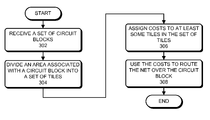
- FIG. 3 presents a flowchart that illustrates a process for routing nets in a hierarchical circuit design in accordance with an embodiment of the present invention.
- the process can begin by receiving a set of circuit blocks (step 302 ).
- One or more circuit blocks can each include a set of terminals, and at least some terminals from the same or different circuit blocks are desired to be electrically linked together using a net which is expected to be routed over one or more circuit blocks.
- the system can then divide an area associated with a circuit block into a set of tiles (step 304 ).
- the shapes and dimensions of the tiles can partially or fully depend on one or more factors.
- the system can assign costs to at least some tiles in the set of tiles (step 306 ).
- the costs can partially or fully depend on one or more factors.
- the system can then use the costs to route the net over the block (step 308 ). Note that using the costs of the tiles during routing makes it more likely that buffers can be used wherever required to meet slew and timing requirements.
- the system can dynamically change the costs during routing. For example, as the routing process progresses, the system may determine that the current assignment of costs to the tiles may lead to a sub-optimal set of routes, and in response to such a determination, the system may adjust the costs of the tiles.
- FIGS. 4A-4G illustrate how tiling can be used to route nets over circuit blocks in accordance with an embodiment of the present invention.
- circuit design 400 can include circuit blocks 402 , 404 , and 406 .
- Terminal 408 in circuit block 402 may be desired to be electrically linked with terminal 410 in circuit block 406 .
- the system can divide an area associated with a circuit block into a set of tiles.
- FIG. 4B illustrates how area 414 , which is associated with circuit block 404 , can be divided into a set of tiles.
- area 414 can be an area in a layer which is situated above or below block 404 .
- area 414 can be in a metal layer that is located above block 404 .
- the shape and dimensions of a tile can depend on a variety of factors. Specifically, the shape and dimensions of a tile can at least partially depend on which semiconductor manufacturing process is used for manufacturing the circuit design, which metal layer the tile is located on, and which block the tile is located on. For example, at higher metal layers, the system may use larger tiles because the signal strength may not deteriorate with distance as quickly as it does at lower metal layers. Similarly, if the semiconductor manufacturing process is expected to result in chips that have low parasitic capacitances, the system may use larger tiles.
- the shape and dimensions of a tile may also depend on a tradeoff between the quality of the routed circuit design and the performance of the routing process. In general, a smaller tile size may improve the quality of the routing solution because of the higher resolution, but may decrease performance because the routing process has to process a larger number of tiles. On the other hand, a larger tile size may decrease the quality of the routing solution because of the lower resolution, but may increase performance because there are fewer tiles.
- FIG. 4C illustrates a tiling that is different from the tiling shown in FIG. 4B .
- the set of tiles includes a large rectangular-shaped tile, namely tile 418 , which is surrounded by smaller square-shaped tiles.
- the system may assign a higher cost to a tile if the tile is located on a lower metal layer, but assign a lower cost to a tile if the tile is located on a higher metal layer.
- a cost assignment can cause the system to route long nets on higher metal layers and short nets on lower metal layers.
- the system may assign a low cost to the tile, whereas if the tile is far from a buffer, the system may assign a high cost.
- FIG. 4F illustrates how net 412 can be routed over circuit block 404 to electrically link terminals 408 and 410 . Note that net 412 has been routed along the edge of circuit block 404 because the routing process used the costs of the tiles to determine the route.
- FIG. 4G illustrates how a buffer can be added to net 412 to ensure that it meets the slew and/or timing requirements. Buffer 420 can be placed outside the edge of circuit block 404 , and net 412 can be routed via buffer 420 to ensure that it meets its slew and/or timing requirements.
- FIG. 5 illustrates a computer system in accordance with an embodiment of the present invention.
- a computer system can generally be any system that can perform computations.
- a computer system can be a microprocessor, a portable computing device, a personal organizer, or any other system, now known or later developed, that can perform computations.
- Computer system 502 comprises processor 504 , memory 506 , and storage 508 .
- Computer system 502 can be coupled with display 514 , keyboard 510 , and pointing device 512 .
- Storage 508 can generally be any device that can store data. Specifically, a storage device can be a magnetic, an optical, or a magneto-optical storage device, or it can be based on flash memory and/or battery-backed up memory. Storage 508 can store applications 516 , operating system 518 , and data 520 .
- Applications 516 can include a routing tool to route nets in a hierarchical circuit design.
- Data 520 can include a circuit description, a circuit block abstraction, user parameters, technology data, a routed circuit design, or any other information that is an input or an output of an application that routes nets in a hierarchical circuit design.
- FIG. 6 illustrates an apparatus in accordance with an embodiment of the present invention.
- Apparatus 602 can comprise a number of mechanisms which may communicate with one another via a wired or wireless communication channel.
- Apparatus 602 may be realized using one or more integrated circuits, and it may be integrated in a computer system, or it may be realized as a separate device which is capable of communicating with other computer systems and/or devices.
- apparatus 602 can comprise receiving mechanism 604 , floorplanning mechanism 606 , tiling mechanism 608 , assigning mechanism 610 , and routing mechanism 612 .
- receiving mechanism 604 may be configured to receive a set of circuit blocks
- floorplanning mechanism 606 may be configured to generate a floorplan
- tiling mechanism 608 may be configured to divide an area associated with a circuit block into a set of tiles
- assigning mechanism 610 may be configured to assign costs to the set of tiles
- routing mechanism 612 may be configured to use the costs to route nets over the circuit blocks.
Abstract
Description
Claims (20)
Priority Applications (1)
| Application Number | Priority Date | Filing Date | Title |
|---|---|---|---|
| US12/490,023 US8255855B2 (en) | 2009-06-23 | 2009-06-23 | Routing nets over circuit blocks in a hierarchical circuit design |
Applications Claiming Priority (1)
| Application Number | Priority Date | Filing Date | Title |
|---|---|---|---|
| US12/490,023 US8255855B2 (en) | 2009-06-23 | 2009-06-23 | Routing nets over circuit blocks in a hierarchical circuit design |
Publications (2)
| Publication Number | Publication Date |
|---|---|
| US20100325600A1 US20100325600A1 (en) | 2010-12-23 |
| US8255855B2 true US8255855B2 (en) | 2012-08-28 |
Family
ID=43355406
Family Applications (1)
| Application Number | Title | Priority Date | Filing Date |
|---|---|---|---|
| US12/490,023 Active 2030-07-12 US8255855B2 (en) | 2009-06-23 | 2009-06-23 | Routing nets over circuit blocks in a hierarchical circuit design |
Country Status (1)
| Country | Link |
|---|---|
| US (1) | US8255855B2 (en) |
Families Citing this family (1)
| Publication number | Priority date | Publication date | Assignee | Title |
|---|---|---|---|---|
| US8762919B2 (en) * | 2009-12-09 | 2014-06-24 | International Business Machines Corporation | Circuit macro placement using macro aspect ratio based on ports |
Citations (11)
| Publication number | Priority date | Publication date | Assignee | Title |
|---|---|---|---|---|
| US20020184607A1 (en) * | 2001-04-19 | 2002-12-05 | International Business Machines Corporation | Practical methodology for early buffer and wire resource allocation |
| US20040216072A1 (en) * | 2003-04-17 | 2004-10-28 | International Business Machines Corporation | Porosity aware buffered steiner tree construction |
| US20050138578A1 (en) * | 2003-12-17 | 2005-06-23 | International Business Machines Corporation | Method and apparatus for generating steiner trees using simultaneous blockage avoidance, delay optimization and design density management |
| US20050138589A1 (en) * | 2003-12-17 | 2005-06-23 | International Business Machines Corporation | Method and apparatus for performing density-biased buffer insertion in an integrated circuit design |
| US20070256045A1 (en) * | 2006-04-28 | 2007-11-01 | Shyh-Chang Lin | V-shaped multilevel full-chip gridless routing |
| US20080134119A1 (en) * | 2006-11-30 | 2008-06-05 | Youang Pin Chen | Automated Electrostatic Discharge Structure Placement and Routing in an Integrated Circuit |
| US20080256502A1 (en) * | 2007-04-11 | 2008-10-16 | International Business Machines Corporation | System and method for global circuit routing incorporating estimation of critical area estimate metrics |
| US20100058268A1 (en) * | 2008-08-28 | 2010-03-04 | Gene Fein | Layout determination |
| US20100077372A1 (en) * | 2008-09-25 | 2010-03-25 | International Business Machines Corporation | Apparatus, Method and Computer Program Product for Fast Stimulation of Manufacturing Effects During Integrated Circuit Design |
| US20100181685A1 (en) * | 2009-01-16 | 2010-07-22 | Sun Microsystems, Inc. | Integrated clock and power distribution |
| US20100257503A1 (en) * | 2009-04-02 | 2010-10-07 | International Business Machines Corporation | Post-routing coupling fixes for integrated circuits |
-
2009
- 2009-06-23 US US12/490,023 patent/US8255855B2/en active Active
Patent Citations (11)
| Publication number | Priority date | Publication date | Assignee | Title |
|---|---|---|---|---|
| US20020184607A1 (en) * | 2001-04-19 | 2002-12-05 | International Business Machines Corporation | Practical methodology for early buffer and wire resource allocation |
| US20040216072A1 (en) * | 2003-04-17 | 2004-10-28 | International Business Machines Corporation | Porosity aware buffered steiner tree construction |
| US20050138578A1 (en) * | 2003-12-17 | 2005-06-23 | International Business Machines Corporation | Method and apparatus for generating steiner trees using simultaneous blockage avoidance, delay optimization and design density management |
| US20050138589A1 (en) * | 2003-12-17 | 2005-06-23 | International Business Machines Corporation | Method and apparatus for performing density-biased buffer insertion in an integrated circuit design |
| US20070256045A1 (en) * | 2006-04-28 | 2007-11-01 | Shyh-Chang Lin | V-shaped multilevel full-chip gridless routing |
| US20080134119A1 (en) * | 2006-11-30 | 2008-06-05 | Youang Pin Chen | Automated Electrostatic Discharge Structure Placement and Routing in an Integrated Circuit |
| US20080256502A1 (en) * | 2007-04-11 | 2008-10-16 | International Business Machines Corporation | System and method for global circuit routing incorporating estimation of critical area estimate metrics |
| US20100058268A1 (en) * | 2008-08-28 | 2010-03-04 | Gene Fein | Layout determination |
| US20100077372A1 (en) * | 2008-09-25 | 2010-03-25 | International Business Machines Corporation | Apparatus, Method and Computer Program Product for Fast Stimulation of Manufacturing Effects During Integrated Circuit Design |
| US20100181685A1 (en) * | 2009-01-16 | 2010-07-22 | Sun Microsystems, Inc. | Integrated clock and power distribution |
| US20100257503A1 (en) * | 2009-04-02 | 2010-10-07 | International Business Machines Corporation | Post-routing coupling fixes for integrated circuits |
Also Published As
| Publication number | Publication date |
|---|---|
| US20100325600A1 (en) | 2010-12-23 |
Similar Documents
| Publication | Publication Date | Title |
|---|---|---|
| CN107863122B (en) | Three-dimensional memory control circuit | |
| US8677302B2 (en) | Multi-threaded detailed routing | |
| US8739104B1 (en) | Systems and methods for forming an integrated circuit using a standard cell library | |
| US9576098B2 (en) | Lithography aware leakage analysis | |
| US9147030B2 (en) | Multiple-instantiated-module (mim) aware pin assignment | |
| US9183335B2 (en) | Dynamic power driven clock tree synthesis (CTS) | |
| US8234605B2 (en) | Minimal leakage-power standard cell library | |
| US10698614B2 (en) | Memory system and operating method thereof | |
| US8689170B2 (en) | Changing the location of a buffer bay in a netlist | |
| US8572541B2 (en) | Method and system for adaptive physical design | |
| US8762919B2 (en) | Circuit macro placement using macro aspect ratio based on ports | |
| US7155693B1 (en) | Floorplanning a hierarchical physical design to improve placement and routing | |
| US20080148213A1 (en) | Routing method for reducing coupling between wires of an electronic circuit | |
| US8255855B2 (en) | Routing nets over circuit blocks in a hierarchical circuit design | |
| US6477696B2 (en) | Routing definition to optimize layout design of standard cells | |
| US20220343053A1 (en) | Semiconductor structure of cell array with adaptive threshold voltage | |
| CN111147068A (en) | Full-adder integrated circuit, four-input multiplexer integrated circuit and using method thereof | |
| US8006208B2 (en) | Reducing coupling between wires of an electronic circuit | |
| US20210064807A1 (en) | Methods of designing layouts of semiconductor devices | |
| KR20180010860A (en) | Semiconductor device having a column decoder | |
| US20180322235A1 (en) | Field-effect transistor placement optimization for improved leaf cell routability | |
| US20230267259A1 (en) | System and method employing power-optimized timing closure | |
| US20220309225A1 (en) | Metal Routing Techniques | |
| JP2007219859A (en) | Method for designing semiconductor integrated circuit | |
| CN114530446A (en) | Semiconductor structure and method for providing unit array |
Legal Events
| Date | Code | Title | Description |
|---|---|---|---|
| AS | Assignment |
Owner name: SUN MICROSYSTEMS, INC., CALIFORNIA Free format text: ASSIGNMENT OF ASSIGNORS INTEREST;ASSIGNORS:WU, YI;HUANG, DAJEN;HOLDBROOK, KALON S.;REEL/FRAME:022998/0996 Effective date: 20090618 |
|
| FEPP | Fee payment procedure |
Free format text: PAYOR NUMBER ASSIGNED (ORIGINAL EVENT CODE: ASPN); ENTITY STATUS OF PATENT OWNER: LARGE ENTITY |
|
| STCF | Information on status: patent grant |
Free format text: PATENTED CASE |
|
| AS | Assignment |
Owner name: ORACLE AMERICA, INC., CALIFORNIA Free format text: MERGER AND CHANGE OF NAME;ASSIGNORS:ORACLE USA, INC.;SUN MICROSYSTEMS, INC.;ORACLE AMERICA, INC.;REEL/FRAME:037311/0182 Effective date: 20100212 |
|
| FPAY | Fee payment |
Year of fee payment: 4 |
|
| MAFP | Maintenance fee payment |
Free format text: PAYMENT OF MAINTENANCE FEE, 8TH YEAR, LARGE ENTITY (ORIGINAL EVENT CODE: M1552); ENTITY STATUS OF PATENT OWNER: LARGE ENTITY Year of fee payment: 8 |
|
| MAFP | Maintenance fee payment |
Free format text: PAYMENT OF MAINTENANCE FEE, 12TH YEAR, LARGE ENTITY (ORIGINAL EVENT CODE: M1553); ENTITY STATUS OF PATENT OWNER: LARGE ENTITY Year of fee payment: 12 |