US8263235B2 - Organic light emitting device having a high light extraction efficiency - Google Patents
Organic light emitting device having a high light extraction efficiency Download PDFInfo
- Publication number
- US8263235B2 US8263235B2 US12/144,389 US14438908A US8263235B2 US 8263235 B2 US8263235 B2 US 8263235B2 US 14438908 A US14438908 A US 14438908A US 8263235 B2 US8263235 B2 US 8263235B2
- Authority
- US
- United States
- Prior art keywords
- light emitting
- poly
- organic light
- emitting device
- layer
- Prior art date
- Legal status (The legal status is an assumption and is not a legal conclusion. Google has not performed a legal analysis and makes no representation as to the accuracy of the status listed.)
- Expired - Fee Related, expires
Links
- 0 Cc1cc(N(c2cccc(*)c2)c2cc(N(c3cccc(C)c3)c3cc(*)ccc3)ccc2)ccc1 Chemical compound Cc1cc(N(c2cccc(*)c2)c2cc(N(c3cccc(C)c3)c3cc(*)ccc3)ccc2)ccc1 0.000 description 2
- QZTROBFEPMSEPK-HHLKWOBFSA-N C.C1=CC2=C(C=C1)/C1=N/C3=C4C=CC=CC4=C4/N=C5/C6=C(C=CC=C6)C6=N5[C@@]5(N34)N1=C2N=C1C2=C(C=CC=C2)/C(=N/6)[N@@]15.C1=CC=C(N(C2=CC=C(C3=CC=C(N(C4=CC=CC=C4)C4=C5C=CC=CC5=CC=C4)C=C3)C=C2)C2=CC=CC3=C2C=CC=C3)C=C1.CC1=CC=CC(N(C2=CC=CC=C2)C2=CC=C(C3=CC=C(N(C4=CC=CC=C4)C4=CC=CC(C)=C4)C=C3)C=C2)=C1.CC1=CC=CC(N(C2=CC=CC=C2)C2=CC=C(N(C3=CC=C(N(C4=CC=CC=C4)C4=CC(C)=CC=C4)C=C3)C3=CC=C(N(C4=CC=CC=C4)C4=CC(C)=CC=C4)C=C3)C=C2)=C1.[2H]P[3H] Chemical compound C.C1=CC2=C(C=C1)/C1=N/C3=C4C=CC=CC4=C4/N=C5/C6=C(C=CC=C6)C6=N5[C@@]5(N34)N1=C2N=C1C2=C(C=CC=C2)/C(=N/6)[N@@]15.C1=CC=C(N(C2=CC=C(C3=CC=C(N(C4=CC=CC=C4)C4=C5C=CC=CC5=CC=C4)C=C3)C=C2)C2=CC=CC3=C2C=CC=C3)C=C1.CC1=CC=CC(N(C2=CC=CC=C2)C2=CC=C(C3=CC=C(N(C4=CC=CC=C4)C4=CC=CC(C)=C4)C=C3)C=C2)=C1.CC1=CC=CC(N(C2=CC=CC=C2)C2=CC=C(N(C3=CC=C(N(C4=CC=CC=C4)C4=CC(C)=CC=C4)C=C3)C3=CC=C(N(C4=CC=CC=C4)C4=CC(C)=CC=C4)C=C3)C=C2)=C1.[2H]P[3H] QZTROBFEPMSEPK-HHLKWOBFSA-N 0.000 description 1
- LUJPCTSWCSQZOK-UHFFFAOYSA-N C.C1=CC=C(N(C2=CC=CC=C2)C2=CC=C3C(=C2)C2(C4=CC(N(C5=CC=CC=C5)C5=CC=CC=C5)=CC=C4C4=C2C=C(N(C2=CC=CC=C2)C2=CC=CC=C2)C=C4)C2=C3C=CC(N(C3=CC=CC=C3)C3=CC=CC=C3)=C2)C=C1.CC1=CC=C(N(C2=CC=C(C)C=C2)C2=CC=C(C3(C4=CC=C(N(C5=CC=C(C)C=C5)C5=CC=C(C)C=C5)C=C4)CCCCC3)C=C2)C=C1.CC1=CC=CC(N(C2=CC=CC(N(C3=CC=CC(C)=C3)C3=CC=CC(C)=C3)=C2)C2=CC(C)=CC=C2)=C1.CC1=CC=CC(N(C2=CC=CC=C2)C2=CC3=C(C=C2)C2=CC=C(N(C4=CC=CC=C4)C4=CC=CC(C)=C4)C=C2C3(C)C)=C1 Chemical compound C.C1=CC=C(N(C2=CC=CC=C2)C2=CC=C3C(=C2)C2(C4=CC(N(C5=CC=CC=C5)C5=CC=CC=C5)=CC=C4C4=C2C=C(N(C2=CC=CC=C2)C2=CC=CC=C2)C=C4)C2=C3C=CC(N(C3=CC=CC=C3)C3=CC=CC=C3)=C2)C=C1.CC1=CC=C(N(C2=CC=C(C)C=C2)C2=CC=C(C3(C4=CC=C(N(C5=CC=C(C)C=C5)C5=CC=C(C)C=C5)C=C4)CCCCC3)C=C2)C=C1.CC1=CC=CC(N(C2=CC=CC(N(C3=CC=CC(C)=C3)C3=CC=CC(C)=C3)=C2)C2=CC(C)=CC=C2)=C1.CC1=CC=CC(N(C2=CC=CC=C2)C2=CC3=C(C=C2)C2=CC=C(N(C4=CC=CC=C4)C4=CC=CC(C)=C4)C=C2C3(C)C)=C1 LUJPCTSWCSQZOK-UHFFFAOYSA-N 0.000 description 1
- MZTLDOJNEMNXFH-KFXQWTQDSA-N C/C=C/C1=CC(OC)=C(C)C=C1OCC(CC)CCCC.C/C=C/C1=CC=C(C)C=C1.CCCCCCC1=C(C)C=CC(C)=N1.CCCCCCCCCCCCC1(CCCCCCCCCCCC)C2=CC(C)=CC=C2C2=CC=C(C)C=C21.CCCCCCCCCCCCC1=C(C)C=CC(C)=C1.[C-]#[N+]/C(=C\C1=CC(OCCCCCC)=C(C)C=C1OCCCCCC)C1=CC(OCCCCCC)=C(/C(C#N)=C/C)C=C1OCCCCCC Chemical compound C/C=C/C1=CC(OC)=C(C)C=C1OCC(CC)CCCC.C/C=C/C1=CC=C(C)C=C1.CCCCCCC1=C(C)C=CC(C)=N1.CCCCCCCCCCCCC1(CCCCCCCCCCCC)C2=CC(C)=CC=C2C2=CC=C(C)C=C21.CCCCCCCCCCCCC1=C(C)C=CC(C)=C1.[C-]#[N+]/C(=C\C1=CC(OCCCCCC)=C(C)C=C1OCCCCCC)C1=CC(OCCCCCC)=C(/C(C#N)=C/C)C=C1OCCCCCC MZTLDOJNEMNXFH-KFXQWTQDSA-N 0.000 description 1
- HJWXFXCKHKBTCB-BQKLGDEUSA-N C1=C2=CC=C3=CC=C4=CC=C5=CC=C6=CC=C(=C1)C1=C2C3=C4C5=C16.C1=CC=C(C2=C3C=CC=CC3=C(C3=CC=CC=C3)C3=C(C4=CC=CC=C4)C4=CC=CC=C4C(C4=CC=CC=C4)=C23)C=C1.C1=CC=C(N(C2=CC=CC=C2)C2=CC=C(C=CC3=CC=C(C4=CC=C(C=CC5=CC=C(N(C6=CC=CC=C6)C6=CC=CC=C6)C=C5)C=C4)C=C3)C=C2)C=C1.CCN(CC)C1=CC2=C(C=C1)C=C(C1=NC3=C(C=CC=C3)S1)C(=O)O2.CCN(CC)C1=CC2=C(C=C1)N=C1C(=CC(=O)C3=C1C=CC=C3)O2.O=C1C2=CC3=C(C=C2NC2=C1C=CC=C2)C(=O)C1=C(C=CC=C1)N3.[C-]#[N+]/C(C#N)=C1\C=C(C)OC(/C=C/C2=CC=C(N(CC)CC)C=C2)=C1 Chemical compound C1=C2=CC=C3=CC=C4=CC=C5=CC=C6=CC=C(=C1)C1=C2C3=C4C5=C16.C1=CC=C(C2=C3C=CC=CC3=C(C3=CC=CC=C3)C3=C(C4=CC=CC=C4)C4=CC=CC=C4C(C4=CC=CC=C4)=C23)C=C1.C1=CC=C(N(C2=CC=CC=C2)C2=CC=C(C=CC3=CC=C(C4=CC=C(C=CC5=CC=C(N(C6=CC=CC=C6)C6=CC=CC=C6)C=C5)C=C4)C=C3)C=C2)C=C1.CCN(CC)C1=CC2=C(C=C1)C=C(C1=NC3=C(C=CC=C3)S1)C(=O)O2.CCN(CC)C1=CC2=C(C=C1)N=C1C(=CC(=O)C3=C1C=CC=C3)O2.O=C1C2=CC3=C(C=C2NC2=C1C=CC=C2)C(=O)C1=C(C=CC=C1)N3.[C-]#[N+]/C(C#N)=C1\C=C(C)OC(/C=C/C2=CC=C(N(CC)CC)C=C2)=C1 HJWXFXCKHKBTCB-BQKLGDEUSA-N 0.000 description 1
- BUKDNXRBEPPZHT-RWETVVEWSA-N C1=CC2=C(C=C1)C1=N(C3=C(C=CC=C3)O1)[C@]1(O2)OC2=C(C=CC=C2)/C2=N\1C1=C(C=CC=C1)O2.C1=CC2=C(C=C1)C1=N(C3=C(C=CC=C3)S1)[C@]1(O2)OC2=C(C=CC=C2)/C2=N\1C1=C(C=CC=C1)S2.C1=CC2=CC=CC3=C2C(=C1)C12(O3)(OC3=C4C(=CC=C3)C=CC=N41)OC1=C3C(=CC=C1)/C=C\C=N/32.C1=CC2=CC=CC3=C2N(=C1)[C@@]1(O3)OC2=C3C(=CC=C2)/C=C\C=N/31.C1=CC=C(C2=C3C=CC=N4C3=C(C=C2)OC42OC3=C4C(=C(C5=CC=CC=C5)C=C3)/C=C\C=N/42)C=C1.CC1=N2C3=C(C=CC=C3C=C1)OC21(OC2=CC=C(C3=CC=CC=C3)C=C2)OC2=C3C(=CC=C2)/C=C\C(C)=N/31 Chemical compound C1=CC2=C(C=C1)C1=N(C3=C(C=CC=C3)O1)[C@]1(O2)OC2=C(C=CC=C2)/C2=N\1C1=C(C=CC=C1)O2.C1=CC2=C(C=C1)C1=N(C3=C(C=CC=C3)S1)[C@]1(O2)OC2=C(C=CC=C2)/C2=N\1C1=C(C=CC=C1)S2.C1=CC2=CC=CC3=C2C(=C1)C12(O3)(OC3=C4C(=CC=C3)C=CC=N41)OC1=C3C(=CC=C1)/C=C\C=N/32.C1=CC2=CC=CC3=C2N(=C1)[C@@]1(O3)OC2=C3C(=CC=C2)/C=C\C=N/31.C1=CC=C(C2=C3C=CC=N4C3=C(C=C2)OC42OC3=C4C(=C(C5=CC=CC=C5)C=C3)/C=C\C=N/42)C=C1.CC1=N2C3=C(C=CC=C3C=C1)OC21(OC2=CC=C(C3=CC=CC=C3)C=C2)OC2=C3C(=CC=C2)/C=C\C(C)=N/31 BUKDNXRBEPPZHT-RWETVVEWSA-N 0.000 description 1
- HXSQPNIFZMVUOO-ASVPMHMXSA-N C1=CC2=C3C4=C(C=CC=C4C=C2)OC2(OC4=C5C(=CC=C4)C=CC4=C5N2=CC=C4)N3=C1.C1=CC2=CC3=C4C(=C2C=C1)C=CC=N4C12(O3)(OC3=C4C(=C5C=CC=CC5=C3)C=CC=N41)OC1=C3C(=C4C=CC=CC4=C1)/C=C\C=N/32.C1=CC=C2C(=C1)C1=N(C=CC=C1)[Ir]213(C2=CC=CC=C2C2=N1C=CC=C2)C1=CC=CC=C1C1=N3C=CC=C1 Chemical compound C1=CC2=C3C4=C(C=CC=C4C=C2)OC2(OC4=C5C(=CC=C4)C=CC4=C5N2=CC=C4)N3=C1.C1=CC2=CC3=C4C(=C2C=C1)C=CC=N4C12(O3)(OC3=C4C(=C5C=CC=CC5=C3)C=CC=N41)OC1=C3C(=C4C=CC=CC4=C1)/C=C\C=N/32.C1=CC=C2C(=C1)C1=N(C=CC=C1)[Ir]213(C2=CC=CC=C2C2=N1C=CC=C2)C1=CC=CC=C1C1=N3C=CC=C1 HXSQPNIFZMVUOO-ASVPMHMXSA-N 0.000 description 1
- ZCKNYMWAIUWGCP-UHFFFAOYSA-N C1=CC=C(C2=CC=NC3=C4N=CC=C(C5=CC=CC=C5)C4=CC=C23)C=C1.CBP.CC(C)(C)C1=CC=C(C2=NN=C(C3=CC=C(C4=CC=CC=C4)C=C3)N2C2=CC=CC=C2)C=C1.CC(C)(C)C1=CC=C(C2=NN=C(C3=CC=CC(C4=NN=C(C5=CC=C(C(C)(C)C)C=C5)O4)=C3)O2)C=C1.CC1=CC=C(C(=CC2=C3C=CC=CC3=C(C=C(C3=CC=C(C)C=C3)C3=CC=C(C)C=C3)C3=CC=CC=C32)C2=CC=C(C)C=C2)C=C1.CC1=CC=C(C(=CC2=CC=C(C3=CC=C(C=C(C4=CC=C(C)C=C4)C4=CC=C(C)C=C4)C=C3)C=C2)C2=CC=C(C)C=C2)C=C1.CC1=NC2=C3N=C(C)C=C(C4=CC=CC=C4)C3=CC=C2C(C2=CC=CC=C2)=C1.O=C1C2=C3C(=CC=C4C3=C(/C=C\2)C2=C3C5=C(C=C2)C2=NC6=C(C=CC=C6)N2C(=O)/C5=C/C=C/43)C2=NC3=C(C=CC=C3)N12 Chemical compound C1=CC=C(C2=CC=NC3=C4N=CC=C(C5=CC=CC=C5)C4=CC=C23)C=C1.CBP.CC(C)(C)C1=CC=C(C2=NN=C(C3=CC=C(C4=CC=CC=C4)C=C3)N2C2=CC=CC=C2)C=C1.CC(C)(C)C1=CC=C(C2=NN=C(C3=CC=CC(C4=NN=C(C5=CC=C(C(C)(C)C)C=C5)O4)=C3)O2)C=C1.CC1=CC=C(C(=CC2=C3C=CC=CC3=C(C=C(C3=CC=C(C)C=C3)C3=CC=C(C)C=C3)C3=CC=CC=C32)C2=CC=C(C)C=C2)C=C1.CC1=CC=C(C(=CC2=CC=C(C3=CC=C(C=C(C4=CC=C(C)C=C4)C4=CC=C(C)C=C4)C=C3)C=C2)C2=CC=C(C)C=C2)C=C1.CC1=NC2=C3N=C(C)C=C(C4=CC=CC=C4)C3=CC=C2C(C2=CC=CC=C2)=C1.O=C1C2=C3C(=CC=C4C3=C(/C=C\2)C2=C3C5=C(C=C2)C2=NC6=C(C=CC=C6)N2C(=O)/C5=C/C=C/43)C2=NC3=C(C=CC=C3)N12 ZCKNYMWAIUWGCP-UHFFFAOYSA-N 0.000 description 1
- KTNQIYAVHUYNPE-UHFFFAOYSA-N CCC1(CC)C2=C(C=CC(C3=C/C4=C(\C=C/3)C3=C(C=C(C5=C/C6=C(\C=C/5)C5=C(C=C(C7=C/C8=C(\C=C/7)C7=C(C=C(C9=C/C%10=C(\C=C/9)C9=C(C=C(C%11=C/C%12=C(\C=C/%11)C%11=C(C=CC=C%11)C%12(CC)CC)C=C9)C%10(CC)CC)C=C7)C8(CC)CC)C=C5)C6(CC)CC)C=C3)C4(CC)CC)=C2)C2=C1/C=C\C=C/2 Chemical compound CCC1(CC)C2=C(C=CC(C3=C/C4=C(\C=C/3)C3=C(C=C(C5=C/C6=C(\C=C/5)C5=C(C=C(C7=C/C8=C(\C=C/7)C7=C(C=C(C9=C/C%10=C(\C=C/9)C9=C(C=C(C%11=C/C%12=C(\C=C/%11)C%11=C(C=CC=C%11)C%12(CC)CC)C=C9)C%10(CC)CC)C=C7)C8(CC)CC)C=C5)C6(CC)CC)C=C3)C4(CC)CC)=C2)C2=C1/C=C\C=C/2 KTNQIYAVHUYNPE-UHFFFAOYSA-N 0.000 description 1
- JERUGJKGRPVMEQ-UHFFFAOYSA-N CCCC1(CCC(C)C)C2=C(C=CC(C3=C/C4=C(\C=C/3)C3=C(C=C(C5=C/C6=C(\C=C/5)C5=C(C=C(C7=C/C8=C(\C=C/7)C7=C(C=C(C9=C/C%10=C(\C=C/9)C9=C(C=C(C%11=C/C%12=C(\C=C/%11)C%11=C(C=C(C%13=C/C%14=C(\C=C/%13)C%13=C(C=C(C%15=C/C%16=C(\C=C/%15)C%15=C(C=C(C%17=C/C%18=C(\C=C/%17)C%17=C(C=CC=C%17)C%18(CCC(C)C)CCC(C)C)C=C%15)C%16(C)C)C=C%13)C%14(CCC(C)C)CCC(C)C)C=C%11)C%12(CCC(C)C)CCC(C)C)C=C9)C%10(C)C)C=C7)C8(CC)CCC(C)C)C=C5)C6(CCC)CCC(C)C)C=C3)C4(C)C)=C2)C2=C1/C=C\C=C/2.CCCCC1=CC=C2C(=C1)[Ir]N1=CC=C3C=CC=CC3=C21 Chemical compound CCCC1(CCC(C)C)C2=C(C=CC(C3=C/C4=C(\C=C/3)C3=C(C=C(C5=C/C6=C(\C=C/5)C5=C(C=C(C7=C/C8=C(\C=C/7)C7=C(C=C(C9=C/C%10=C(\C=C/9)C9=C(C=C(C%11=C/C%12=C(\C=C/%11)C%11=C(C=C(C%13=C/C%14=C(\C=C/%13)C%13=C(C=C(C%15=C/C%16=C(\C=C/%15)C%15=C(C=C(C%17=C/C%18=C(\C=C/%17)C%17=C(C=CC=C%17)C%18(CCC(C)C)CCC(C)C)C=C%15)C%16(C)C)C=C%13)C%14(CCC(C)C)CCC(C)C)C=C%11)C%12(CCC(C)C)CCC(C)C)C=C9)C%10(C)C)C=C7)C8(CC)CCC(C)C)C=C5)C6(CCC)CCC(C)C)C=C3)C4(C)C)=C2)C2=C1/C=C\C=C/2.CCCCC1=CC=C2C(=C1)[Ir]N1=CC=C3C=CC=CC3=C21 JERUGJKGRPVMEQ-UHFFFAOYSA-N 0.000 description 1
- OGEZSLXPCKHGKO-UHFFFAOYSA-N O=C(c(cc1)c(c2ccc3-c(c4c56)ccc5C(N5c7ccccc7)=O)c3c1-c4ccc6C5=O)N(c1ccccc1)C2=O Chemical compound O=C(c(cc1)c(c2ccc3-c(c4c56)ccc5C(N5c7ccccc7)=O)c3c1-c4ccc6C5=O)N(c1ccccc1)C2=O OGEZSLXPCKHGKO-UHFFFAOYSA-N 0.000 description 1
- YQJAOUOFLXCXGA-UHFFFAOYSA-N O=C(c1cccc2c1c-1ccc2)[n]2c-1nc1c2c2ccccc2c2ccccc12 Chemical compound O=C(c1cccc2c1c-1ccc2)[n]2c-1nc1c2c2ccccc2c2ccccc12 YQJAOUOFLXCXGA-UHFFFAOYSA-N 0.000 description 1
- KSILGKJJSBMAEK-UHFFFAOYSA-N O=C1C(C2=CC=CC=C2)=CC(=C2C=C(C3=CC=CC=C3)C(=O)C(C3=CC=CC=C3)=C2)C=C1C1=CC=CC=C1.O=C1C2=C3C(=CC=C2)/C=C\C=C/3C2=NC3=C(C4=C(C=CC=C4)C4=C3C=CC=C4)N12.O=C1C2=C3C4=C(C=C2)C2=C5C6=C(C=C2)C(=O)N(C2=CC=CC=C2)C(=O)/C6=C/C=C5/C4=C/C=C\3C(=O)N1C1=CC=CC=C1 Chemical compound O=C1C(C2=CC=CC=C2)=CC(=C2C=C(C3=CC=CC=C3)C(=O)C(C3=CC=CC=C3)=C2)C=C1C1=CC=CC=C1.O=C1C2=C3C(=CC=C2)/C=C\C=C/3C2=NC3=C(C4=C(C=CC=C4)C4=C3C=CC=C4)N12.O=C1C2=C3C4=C(C=C2)C2=C5C6=C(C=C2)C(=O)N(C2=CC=CC=C2)C(=O)/C6=C/C=C5/C4=C/C=C\3C(=O)N1C1=CC=CC=C1 KSILGKJJSBMAEK-UHFFFAOYSA-N 0.000 description 1
Images


Classifications
-
- C—CHEMISTRY; METALLURGY
- C09—DYES; PAINTS; POLISHES; NATURAL RESINS; ADHESIVES; COMPOSITIONS NOT OTHERWISE PROVIDED FOR; APPLICATIONS OF MATERIALS NOT OTHERWISE PROVIDED FOR
- C09K—MATERIALS FOR MISCELLANEOUS APPLICATIONS, NOT PROVIDED FOR ELSEWHERE
- C09K11/00—Luminescent, e.g. electroluminescent, chemiluminescent materials
- C09K11/06—Luminescent, e.g. electroluminescent, chemiluminescent materials containing organic luminescent materials
-
- H—ELECTRICITY
- H10—SEMICONDUCTOR DEVICES; ELECTRIC SOLID-STATE DEVICES NOT OTHERWISE PROVIDED FOR
- H10K—ORGANIC ELECTRIC SOLID-STATE DEVICES
- H10K50/00—Organic light-emitting devices
- H10K50/10—OLEDs or polymer light-emitting diodes [PLED]
- H10K50/11—OLEDs or polymer light-emitting diodes [PLED] characterised by the electroluminescent [EL] layers
-
- H—ELECTRICITY
- H10—SEMICONDUCTOR DEVICES; ELECTRIC SOLID-STATE DEVICES NOT OTHERWISE PROVIDED FOR
- H10K—ORGANIC ELECTRIC SOLID-STATE DEVICES
- H10K50/00—Organic light-emitting devices
- H10K50/80—Constructional details
- H10K50/85—Arrangements for extracting light from the devices
-
- H—ELECTRICITY
- H10—SEMICONDUCTOR DEVICES; ELECTRIC SOLID-STATE DEVICES NOT OTHERWISE PROVIDED FOR
- H10K—ORGANIC ELECTRIC SOLID-STATE DEVICES
- H10K50/00—Organic light-emitting devices
- H10K50/80—Constructional details
- H10K50/85—Arrangements for extracting light from the devices
- H10K50/858—Arrangements for extracting light from the devices comprising refractive means, e.g. lenses
-
- H—ELECTRICITY
- H10—SEMICONDUCTOR DEVICES; ELECTRIC SOLID-STATE DEVICES NOT OTHERWISE PROVIDED FOR
- H10K—ORGANIC ELECTRIC SOLID-STATE DEVICES
- H10K85/00—Organic materials used in the body or electrodes of devices covered by this subclass
- H10K85/10—Organic polymers or oligomers
- H10K85/111—Organic polymers or oligomers comprising aromatic, heteroaromatic, or aryl chains, e.g. polyaniline, polyphenylene or polyphenylene vinylene
- H10K85/115—Polyfluorene; Derivatives thereof
-
- C—CHEMISTRY; METALLURGY
- C09—DYES; PAINTS; POLISHES; NATURAL RESINS; ADHESIVES; COMPOSITIONS NOT OTHERWISE PROVIDED FOR; APPLICATIONS OF MATERIALS NOT OTHERWISE PROVIDED FOR
- C09K—MATERIALS FOR MISCELLANEOUS APPLICATIONS, NOT PROVIDED FOR ELSEWHERE
- C09K2211/00—Chemical nature of organic luminescent or tenebrescent compounds
- C09K2211/10—Non-macromolecular compounds
- C09K2211/1003—Carbocyclic compounds
- C09K2211/1007—Non-condensed systems
-
- C—CHEMISTRY; METALLURGY
- C09—DYES; PAINTS; POLISHES; NATURAL RESINS; ADHESIVES; COMPOSITIONS NOT OTHERWISE PROVIDED FOR; APPLICATIONS OF MATERIALS NOT OTHERWISE PROVIDED FOR
- C09K—MATERIALS FOR MISCELLANEOUS APPLICATIONS, NOT PROVIDED FOR ELSEWHERE
- C09K2211/00—Chemical nature of organic luminescent or tenebrescent compounds
- C09K2211/10—Non-macromolecular compounds
- C09K2211/1003—Carbocyclic compounds
- C09K2211/1011—Condensed systems
-
- C—CHEMISTRY; METALLURGY
- C09—DYES; PAINTS; POLISHES; NATURAL RESINS; ADHESIVES; COMPOSITIONS NOT OTHERWISE PROVIDED FOR; APPLICATIONS OF MATERIALS NOT OTHERWISE PROVIDED FOR
- C09K—MATERIALS FOR MISCELLANEOUS APPLICATIONS, NOT PROVIDED FOR ELSEWHERE
- C09K2211/00—Chemical nature of organic luminescent or tenebrescent compounds
- C09K2211/10—Non-macromolecular compounds
- C09K2211/1003—Carbocyclic compounds
- C09K2211/1014—Carbocyclic compounds bridged by heteroatoms, e.g. N, P, Si or B
-
- C—CHEMISTRY; METALLURGY
- C09—DYES; PAINTS; POLISHES; NATURAL RESINS; ADHESIVES; COMPOSITIONS NOT OTHERWISE PROVIDED FOR; APPLICATIONS OF MATERIALS NOT OTHERWISE PROVIDED FOR
- C09K—MATERIALS FOR MISCELLANEOUS APPLICATIONS, NOT PROVIDED FOR ELSEWHERE
- C09K2211/00—Chemical nature of organic luminescent or tenebrescent compounds
- C09K2211/10—Non-macromolecular compounds
- C09K2211/1018—Heterocyclic compounds
- C09K2211/1025—Heterocyclic compounds characterised by ligands
- C09K2211/1029—Heterocyclic compounds characterised by ligands containing one nitrogen atom as the heteroatom
- C09K2211/1033—Heterocyclic compounds characterised by ligands containing one nitrogen atom as the heteroatom with oxygen
-
- C—CHEMISTRY; METALLURGY
- C09—DYES; PAINTS; POLISHES; NATURAL RESINS; ADHESIVES; COMPOSITIONS NOT OTHERWISE PROVIDED FOR; APPLICATIONS OF MATERIALS NOT OTHERWISE PROVIDED FOR
- C09K—MATERIALS FOR MISCELLANEOUS APPLICATIONS, NOT PROVIDED FOR ELSEWHERE
- C09K2211/00—Chemical nature of organic luminescent or tenebrescent compounds
- C09K2211/10—Non-macromolecular compounds
- C09K2211/1018—Heterocyclic compounds
- C09K2211/1025—Heterocyclic compounds characterised by ligands
- C09K2211/1088—Heterocyclic compounds characterised by ligands containing oxygen as the only heteroatom
-
- H—ELECTRICITY
- H10—SEMICONDUCTOR DEVICES; ELECTRIC SOLID-STATE DEVICES NOT OTHERWISE PROVIDED FOR
- H10K—ORGANIC ELECTRIC SOLID-STATE DEVICES
- H10K85/00—Organic materials used in the body or electrodes of devices covered by this subclass
- H10K85/10—Organic polymers or oligomers
- H10K85/151—Copolymers
-
- H—ELECTRICITY
- H10—SEMICONDUCTOR DEVICES; ELECTRIC SOLID-STATE DEVICES NOT OTHERWISE PROVIDED FOR
- H10K—ORGANIC ELECTRIC SOLID-STATE DEVICES
- H10K85/00—Organic materials used in the body or electrodes of devices covered by this subclass
- H10K85/30—Coordination compounds
- H10K85/341—Transition metal complexes, e.g. Ru(II)polypyridine complexes
- H10K85/342—Transition metal complexes, e.g. Ru(II)polypyridine complexes comprising iridium
Definitions
- the present invention relates to an organic light emitting device.
- a light extraction efficiency ⁇ at which light generated inside an organic light emitting device is extracted outside thereof depends upon a critical angle ⁇ of a total reflection angle when light is output from a medium having a refractive index of n to the air having a refractive index of 1.00.
- the light emitting layer using an organic light emitting material has a refractive index in a range of 1.7 to 1.8.
- Alq 3 which is a typical light emitting material has a refractive index of 1.70 (Japanese Patent Application Laid-Open No. H07-240277).
- the light extraction efficiency ⁇ is determined to be about 17.3% when 1.70 is substituted for n in Expression (2).
- the light extraction efficiency of an organic light emitting device is determined by the refractive index of a light emitting layer, it has not been reported that the light extraction efficiency of the organic light emitting device is enhanced actually when the refractive index of the light emitting layer is decreased.
- the inventor of the present invention have found that a high light extraction efficiency and excellent initial characteristics and durability can be obtained by decreasing the refractive index of a light emitting layer of an organic light emitting device.
- an organic light emitting device of the present invention includes an anode, a cathode, and a layer formed of an organic compound interposed between the anode and the cathode.
- the layer formed of the organic compound includes a light emitting layer, and the light emitting layer is formed of at least one organic light emitting material and an aliphatic compound, and a refractive index of the light emitting layer is 1.40 or more to 1.60 or less.
- the present invention can provide an organic light emitting device having a high light extraction efficiency and being excellent in an light emitting efficiency and durability.
- FIG. 1 is a view illustrating a relationship between a critical angle ⁇ of a total reflection angle in an organic light emitting device and light extraction to the outside of the device.
- FIG. 2 is a cross-sectional view illustrating a first embodiment in an organic light emitting device of the present invention.
- FIG. 3 is a cross-sectional view illustrating a second embodiment in the organic light emitting device of the present invention.
- FIG. 4 is a cross-sectional view illustrating a third embodiment in the organic light emitting device of the present invention.
- FIG. 5 is a cross-sectional view illustrating a fourth embodiment in the organic light emitting device of the present invention.
- FIG. 6 is a cross-sectional view illustrating a fifth embodiment in the organic light emitting device of the present invention.
- FIG. 7 is a cross-sectional view illustrating a sixth embodiment in the organic light emitting device of the present invention.
- FIG. 8 is a cross-sectional view illustrating a seventh embodiment in the organic light emitting device of the present invention.
- FIG. 9 is a schematic cross-sectional view illustrating an organic light emitting device according to an embodiment of the present invention and a circuit and wiring for driving the device.
- FIG. 10 is a diagram illustrating the detail of the circuit illustrated in FIG. 9 .
- FIG. 11 is a schematic view illustrating the state of a display in which the organic EL device and the circuit illustrated in FIGS. 9 and 10 are arranged in a matrix with each organic EL device and circuit being one pixel.
- FIG. 12 is a schematic view illustrating a configuration in which the display illustrated in FIG. 11 is formed into a display apparatus.
- An organic light emitting device of the present invention includes an anode, a cathode, and a layer formed of an organic compound interposed between the anode and the cathode.
- the layer formed of an organic compound includes a light emitting layer.
- Reference numeral 1 denotes a substrate; 2 , an anode; 3 , a light emitting layer; 4 , a cathode; 5 a hole transporting layer; 6 , an electron transporting layer; 7 , a hole injecting layer; 9 , a hole/exciton blocking layer; and 10 , 20 , 30 , 40 , 50 , 60 and 70 , an organic light emitting device, respectively.
- FIG. 2 is a cross-sectional view illustrating a first embodiment in the organic light emitting device of the present invention.
- the organic light emitting device 10 illustrated in FIG. 2 is obtained by sequentially providing the anode 2 , the light emitting layer 3 , and the cathode 4 on the substrate 1 .
- the organic light emitting device 10 illustrated in FIG. 2 is useful when the light emitting layer 3 is formed of an organic compound having all of a hole transporting ability, an electron transporting ability, and light emitting property.
- the device is useful also when the light emitting layer 3 is formed by mixing organic compounds each having any one of the hole transporting ability, the electron transporting ability, and the light emitting property.
- FIG. 3 is a cross-sectional view illustrating a second embodiment in the organic light emitting device of the present invention.
- the organic light emitting device 20 illustrated in FIG. 3 is sequentially provided with the anode 2 , the hole transporting layer 5 , the electron transporting layer 6 , and the cathode 4 on the substrate 1 .
- the organic light emitting device 20 illustrated in FIG. 3 is useful when the device is used in combination with a light emitting organic compound having one of hole transporting ability and electron transporting ability and an organic compound having a mere electron transporting ability or a mere hole transporting ability.
- the hole transporting layer 5 or the electron transporting layer 6 also works as a light emitting layer.
- FIG. 4 is a cross-sectional view illustrating a third embodiment in the organic light emitting device of the present invention.
- the organic light emitting device 30 illustrated in FIG. 4 is the device in which the light emitting layer 3 was inserted between the hole transporting layer 5 and the electron transporting layer 6 in the organic light emitting device 20 illustrated in FIG. 3 .
- a carrier transporting function and a light emitting function are separated in the organic light emitting device 30 illustrated in FIG. 4 .
- the light emitting device 30 illustrated in FIG. 4 may use an appropriate combination of organic compounds each having any one of a hole transporting ability, an electron transporting ability, and light emitting property. Therefore, the degree of freedom in selection of a material extremely increases, and various organic compounds having different light emission wavelengths can be used. As a result, the range of light emission hue can be widened. Further, a light emitting efficiency of the organic light emitting device 30 illustrated in FIG. 4 can also be improved by effectively confining each carrier or exciton in the central light emitting layer 3 .
- FIG. 5 is a cross-sectional view illustrating a fourth embodiment in the organic light emitting device of the present invention.
- the organic light emitting device 40 illustrated in FIG. 5 is different from the organic light emitting device 30 illustrated in FIG. 4 in that the hole injecting layer 7 is provided between the anode 2 and the hole transporting layer 5 .
- the organic light emitting device 40 illustrated in FIG. 5 is effective in reducing the voltage at which the device is driven because adhesiveness between the anode 2 and the hole transporting layer 5 or hole injecting property is improved by providing the hole injecting layer 7 .
- FIG. 6 is a cross-sectional view illustrating a fifth embodiment of the organic light emitting device of the present invention.
- the organic light emitting device illustrated 50 in FIG. 6 has a configuration in which a hole/exciton blocking layer 9 is provided between the light emitting layer 3 and the electron transporting layer 6 in the organic light emitting device 30 illustrated in FIG. 4 .
- a hole/exciton blocking layer 9 is provided between the light emitting layer 3 and the electron transporting layer 6 in the organic light emitting device 30 illustrated in FIG. 4 .
- the organic light emitting device 50 illustrated in FIG. 6 holes or exitons are suppressed from being output from the light emitting layer 3 to the cathode 4 due to the presence of the hole/exciton blocking layer 9 , so the organic light emitting device 50 illustrated in FIG. 6 is effective for enhancing the light emitting efficiency.
- FIG. 7 is a cross-sectional view illustrating a sixth embodiment of the organic light emitting device of the present invention.
- the organic light emitting device 60 in FIG. 7 has a configuration in which the electron injecting layer 8 is provided between the electron transporting layer 6 and the cathode 4 in the organic light emitting device 40 illustrated in FIG. 5 .
- the organic light emitting device 60 illustrated in FIG. 7 is effective for reducing a voltage due to the presence of the electron injecting layer 8 between the electron transporting layer 6 and the cathode 4 .
- FIG. 8 is a cross-sectional view illustrating a seventh embodiment of the organic light emitting device 70 of the present invention.
- the anode 2 , the hole injecting layer 7 , the light emitting layer 3 , the electron injecting layer 8 , and the cathode 4 are successively provided on the substrate 1 .
- the organic light emitting devices illustrated in FIGS. 2 to 8 have basic device configurations, and the configuration of the organic light emitting device of the present invention is not limited thereto.
- the organic light emitting device of the present invention can have various layer configurations in which an insulating layer, an adhesive layer, or an interference layer is provided on an interface between the electrode and the layer formed of an organic compound, the hole injecting layer or the hole transporting layer is composed of two layers having different ionization potentials, etc.
- the light emitting layer of the organic light emitting device of the present invention is composed of at least one organic light emitting material and an aliphatic compound.
- the organic light emitting material constituting the light emitting layer of the organic light emitting device of the present invention is a fluorescent light emitting material or phosphorescent light emitting material.
- fluorescent light emitting material examples include condensed polycyclic compounds such as rubrene and coronene, heterocyclic compounds such as coumarin 6 and quinacrine, and a complex such as Alq 3 .
- Examples of the phosphorescent light emitting material include complexes containing heavy metal such as an indium complex, an europium complex, and platinum porphyrin.
- the aliphatic compound includes those in which fluorine atoms are substituted for a part or an entirety of hydrogen atoms in molecules (fluorine-containing aliphatic compound) and those in which molecules do not contain fluorine atoms (non-fluorine based aliphatic compound).
- the aliphatic compound does not have an aromatic ring such as a benzene ring. Further, the aliphatic compound is a medium that functions as an insulator, and that holds an organic light emitting material uniformly in the light emitting layer. Here, carriers injected from each electrode reach the organic light emitting material due to the tunnel effects.
- fluorine-containing aliphatic compound there are given a fluorine-containing acrylate polymer and a fluorine-containing vinyl polymer, and the like.
- a non-fluorinated aliphatic compound there are given an oxyalkylene polymer, a vinyl alkyl ether polymer, and the like.
- the light emitting layer of the organic light emitting device of the present invention has a refractive index of 1.40 or more to 1.60 or less.
- n a refractive index
- ⁇ a molecular refraction per molecular volume represented by the following Expression (4). ⁇ 4/3 ⁇ N ⁇ ( ⁇ R/V ) (4)
- N a molecular number in a unit volume
- a a polarizability
- R a molecular refraction
- V a molecular volume represented by the following Expression (5).
- M represents a molecular weight
- ⁇ represents a density
- the refractive index of the light emitting layer is 1.40 or more to 1.60 or less.
- the refractive index is lower compared with the refractive index (about 1.7) of the light emitting layer formed of a known organic light emitting material.
- the refractive index of the light emitting layer can be decreased by including an organic material having a low polarizability (e.g., the above aliphatic compound) in the light emitting layer.
- the refractive index of the light emitting layer is set to be less than 1.4, it is necessary to use a fluorine-containing aliphatic compound having low solubility with respect to a solvent, which makes it difficult to form a light emitting layer. Further, when the refractive index of the light emitting layer is set to be 1.60 or more, the effects of enhancing a light extraction efficiency cannot be obtained sufficiently.
- the fluorine-containing aliphatic compound examples include the above fluorine-containing acrylic polymer and a fluorine-containing vinyl polymer. It should be noted that a fluorine-containing aliphatic compound having a refractive index of less than 1.35 is not suitable as a material constituting a light emitting layer due to the low solubility with respect to a solvent. Further, with the fluorine-based aliphatic compound having a refractive index exceeding 1.47, the effects of enhancing a light extraction efficiency cannot be obtained sufficiently. For the above reasons, the fluorine-containing aliphatic compound used as a material constituting a light emitting layer is preferably selected from those having a refractive index of 1.35 or more to 1.47 or less.
- non-fluorine based aliphatic compound examples include the above oxyalkylene polymer and vinyl alkyl ether polymer.
- the non-fluorine based aliphatic compound having a refractive index of less than 1.43 the kind of a material is limited. Further, with the non-fluorine based aliphatic compound having a refractive index exceeding 1.47, the effects of enhancing a light extraction efficiency cannot be obtained.
- the non-fluorine based aliphatic compound used as a material constituting a light emitting layer is preferably selected from those having a refractive index of 1.43 or more to 1.47 or less.
- the amount of the organic light emitting material constituting the light emitting layer is preferably 2 parts by weight or more to 150 parts by weight or less based on 100 parts by weight of the aliphatic compound. In the case where the amount of the organic light emitting material is less than 2 parts by weight, a current does not flow sufficiently, with the result that sufficient light emission cannot be obtained.
- the refractive index of the light emitting layer is determined by the refractive indices and the mixing ratio of materials. That is, in a light emitting layer formed of an organic light emitting material having a refractive index of 1.7 and an aliphatic compound having a refractive index of less than 1.47, as the contents of the organic light emitting materials increase, the refractive index of the light emitting layer increases accordingly. Thus, in the case where the amount of the organic light emitting material is larger than 150 parts by weight, the refractive index of the light emitting layer increases, with the result that the effects of enhancing a light extraction efficiency cannot be obtained sufficiently.
- the organic light emitting device of the present invention can use known hole transporting compound, light emitting compound, electron transporting compound, and the like in combination.
- exemplary compounds will be illustrated.
- An anode material used in the organic light emitting device of the present invention preferably has as large a work function as possible.
- the anode material that can be used include: metal elements such as gold, silver, platinum, nickel, palladium, cobalt, selenium, and vanadium, and alloys thereof obtained by combining the multiple metal elements; and metal oxides such as tin oxide, zinc oxide, indium tin oxide (ITO), and indium zinc oxide.
- a conductive polymer such as polyaniline, polypyrrole, polythiophene, and polyphenylene sulfide can also be used. Each of those electrode substances may be used alone, or a plurality of the substances may be used in combination.
- the cathode material preferably has as small a work function as possible.
- the cathode material that can be used include metal elements such as lithium, sodium, potassium, cesium, calcium, magnesium, aluminum, indium, silver, lead, tin, and chromium, alloys obtained by combining the multiple metal elements, and salts of those metal elements.
- a metal oxide such as indium tin oxide (ITO) can also be used.
- a cathode may have a single layer constitution or a multilayer constitution.
- a substrate to be used in the organic light emitting device of the present invention is not particularly limited; provided that an opaque substrate such as a metallic substrate or a ceramic substrate, or a transparent substrate such as glass, quartz, or a plastic sheet is used.
- a luminescent color can also be controlled by using a color filter film, a fluorescent color conversion filter film, a dielectric reflective film, or the like as the substrate.
- the produced device may be provided with a protective layer or a sealing layer for the purpose of preventing the device from contacting with oxygen, moisture, or the like.
- the protective layer include: inorganic material films such as a diamond thin film, a metal oxide, and a metal nitride; polymer films such as a fluorine resin, polyparaxylene, polyethylene, a silicone resin, and a polystyrene resin; and a photocurable resin.
- the device itself can be covered with glass, a gas impervious film, metal, or the like, and can be packaged with an appropriate sealing resin.
- the light emitting layer of the present invention is produced by a solution coating method.
- the coating method include spin coating, dispensing, printing, slit coating, an ink jet method, and spraying.
- the thickness of the light emitting layer is determined in view of the emission start voltage and the application voltage of the organic light emitting device, and is less than 10 ⁇ m, preferably 1 ⁇ m or less, and more preferably 30 nm or more to 500 nm or less.
- the organic light emitting device of the present invention may have a plurality of organic layers in addition to the light emitting layer, and examples of the organic layers include a hole injecting layer, a hole transporting layer, a hole/exciton blocking layer, an electron transporting layer, and an electron injecting layer. These layers are produced by vapor deposition or solution coating, and the thickness thereof is less than 5 ⁇ m, preferably 1 ⁇ m or less, and more preferably 10 nm or more to 500 nm or less.
- FIG. 9 is a schematic cross-sectional view illustrating the arrangement of an organic light emitting device on a substrate, a circuit placed outside thereof, and a data wiring.
- the circuit is composed of TFTs, a holding capacitor, and the like.
- the organic light emitting device includes an anode, a cathode, and an organic compound layer 91 placed between the anode and the cathode.
- the organic light emitting device may have, for example, an auxiliary electrode in addition to the anode, the cathode, and the organic compound layer 91 .
- FIG. 9 although only a light emitting device 1 is illustrated, organic light emitting devices are placed two-dimensionally as illustrated in FIG. 11 described later, in the case of constituting a display apparatus.
- FIG. 10 illustrates the detail of the configuration of the circuit illustrated in FIG. 9 .
- the circuit has a typical circuit configuration called a current programming system.
- the circuit of the present invention is not limited thereto.
- a circuit 100 is composed of a drive transistor T 1 , a switching transistor T 2 , a holding capacitor Ch, and an organic light emitting device 11 .
- This is a well-known circuit configuration, so the description of the detail of the operation thereof will be omitted.
- the organic light emitting device can be used as one light emitting point in an exposure light source of a display, an illumination apparatus, and an image forming apparatus of an electrophotographic system.
- reference numeral 12 denotes a data line
- 13 denotes a selection line
- 14 denotes a power source line.
- FIG. 11 schematically illustrates the state in which the organic light emitting device and the circuit illustrated in FIGS. 9 and 10 provided as one pixel are arranged two-dimensionally in a plural number on an identical plane, i.e., the arrangement in a matrix.
- the pixels are connected to a gate driver and a source driver via wiring, and supplied with a driving pulse, whereby the pixels are placed in an emission state or a non-emission state.
- a region in which a plurality of such organic light emitting devices are placed as pixels in the identical plane in an in-plane direction corresponds to a display region. That is, the organic light emitting device of the present embodiment can be used in the display region.
- the display may have any form, as long as it is a display apparatus for a television or a personal computer, or an appliance having a portion displaying an image.
- the display may be a portable display apparatus.
- the display according to the present embodiment can be used in a display portion of an electron imaging apparatus such as a digital camera and a mobile telephone.
- FIG. 12 shows the configuration of a display apparatus formed of the display illustrated in FIG. 11 .
- the display apparatus refers to a configuration in which components required for connection to external appliances such as an interface driver 22 and a connection terminal, and the display illustrated in FIG. 11 are integrated in a housing 23 .
- reference numeral 24 denotes a panel module
- 25 denotes a display region
- 26 denotes a source deriver
- 27 denotes a gate driver.
- An organic light emitting device illustrated in FIG. 8 was produced as follows.
- ITO Indium tin oxide
- substrate 1 glass substrate
- anode 2 was formed into a film on a glass substrate (substrate 1 ) by sputtering, whereby an anode 2 was formed.
- the thickness of the anode 2 was set to be 120 nm.
- the substrate with the ITO formed thereon was washed with an ultrasonic wave successively with acetone and isopropyl alcohol (IPA), and washed by boiling with IPA, followed by drying.
- IPA isopropyl alcohol
- the substrate was further washed with UV/ozone.
- the substrate treated as described above was used as a transparent conductive support substrate.
- Baytron P A1-4083 (manufactured by H.C. Starck Inc.) was formed into a film on the transparent conductive support substrate by spin coating. At this time, the thickness of Bytron was set to be 50 nm. Next, the resultant film was heated at 100° C. for 30 minutes, whereby a hole injecting layer 7 was formed.
- a fluorene compound represented by the following formula 0.5 g was dissolved in 50 g of 1,2-dichloropropane to prepare a mixed solution.
- the mixed solution was applied to the hole injecting layer 7 by spin coating, and heated at 100° C. for one hour, whereby a light emitting layer 3 was formed. At this time, the thickness of the light emitting layer 3 was set to be 100 nm.
- the film thickness of the electron injecting layer 8 was set to be 1 nm
- the vacuum degree during vapor deposition was set to be 1.0 ⁇ 10 ⁇ 4 Pa
- the film forming rate was set to be 0.1 nm/sec.
- the film thickness of the cathode 4 was set to be 150 nm
- the vacuum degree during vapor deposition was set to be 1.0 ⁇ 10 ⁇ 4 Pa
- the film forming rate was set to be 1.0 nm/sec. to 1.2 nm/sec.
- the refractive index of the light emitting layer 3 was measured with a spectral ellipsometer (GES 500 manufactured by SOPRA), or the like.
- GES 500 manufactured by SOPRA
- a glass plate with a film formed thereon separately by the same method as that of the light emitting layer 3 was used.
- the refractive index of the light emitting layer 3 was 1.51. Table 1 shows the results.
- a device was produced by the same method as that of Example 1 except for the above. The obtained device was evaluated in the same way as in Example 1. Further, the refractive index of the light emitting layer 3 was evaluated in the same way as in Example 1. Table 1 shows the results.
- a device was produced by the same method as that of Example 1 except for the above. The obtained device was evaluated in the same way as in Example 1. Further, the refractive index of the light emitting layer 3 was evaluated in the same way as in Example 1. Table 1 shows the results.
- a device was produced by the same method as that of Example 1 except for the above. The obtained device was evaluated in the same way as in Example 1. Further, the refractive index of the light emitting layer 3 was evaluated in the same way as in Example 1. Table 1 shows the results.
- a device was produced by the same method as that of Example 1 except for the above. The obtained device was evaluated in the same way as in Example 1. Further, the refractive index of the light emitting layer 3 was evaluated in the same way as in Example 1. Table 1 shows the results.
- a device was produced by the same method as that of Example 1 except for the above. The obtained device was evaluated in the same way as in Example 1. Further, the refractive index of the light emitting layer 3 was evaluated in the same way as in Example 1. Table 1 shows the results.
- a device was produced by the same method as that of Example 1 except for the above. The obtained device was evaluated in the same way as in Example 1. Further, the refractive index of the light emitting layer 3 was evaluated in the same way as in Example 1. Table 1 shows the results.
- a device was produced by the same method as that of Example 1 except for the above. The obtained device was evaluated in the same way as in Example 1. Further, the refractive index of the light emitting layer 3 was evaluated in the same way as in Example 1. Table 1 shows the results.
- a device was produced by the same method as that of Example 1 except for the above. The obtained device was evaluated in the same way as in Example 1. Further, the refractive index of the light emitting layer 3 was evaluated in the same way as in Example 1. Table 1 shows the results.
- a device was produced by the same method as that of Example 1 except for the above. The obtained device was evaluated in the same way as in Example 1. Further, the refractive index of the light emitting layer 3 was evaluated in the same way as in Example 1. Table 1 shows the results.
- An organic light emitting device illustrated in FIG. 8 was produced as follows.
- a transparent conductive support substrate was produced by the same method as that of Example 1, and the hole injecting layer 7 was formed on the transparent conductive support substrate by the same method as that of Example 1.
- the mixed solution was applied to the above hole injecting layer 7 by spin coating, and heated at 100° C. for 1 hour, whereby a light emitting layer 3 was formed. At this time, the film thickness of the light emitting layer 3 was set to be 100 nm.
- the film thickness of the electron injecting layer 8 was set to be 1 nm, the vacuum degree during vapor deposition was set to be 1.0 ⁇ 10 ⁇ 4 Pa, and the film forming rate was set to be 0.1 nm/sec.
- the film thickness of the cathode 4 was set to be 150 nm
- the vacuum degree during vapor deposition was set to be 1.0 ⁇ 10 ⁇ 4 Pa
- the film forming rate was set to be 1.0 nm/sec. to 1.2 nm/sec.
- the luminance changed from 450 cd/m 2 (initial luminance) to 340 cd/m 2 (after 100 hours). It was found from the result that the degradation in luminance of the organic light emitting device of the present example was small.
- the refractive index of the light emitting layer 3 was measured to be 1.50 by the same method as that in Example 1. Table 2 shows the results.
- a device was produced by the same method as that of Example 9 except for the above. The obtained device was evaluated in the same way as in Example 9. Further, the refractive index of the light emitting layer 3 was evaluated in the same way as in Example 9. Table 2 shows the results.
- a device was produced by the same method as that of Example 9 except for the above. The obtained device was evaluated in the same way as in Example 9. Further, the refractive index of the light emitting layer 3 was evaluated in the same way as in Example 9. Table 2 shows the results.
- a device was produced by the same method as that of Example 9 except for the above. The obtained device was evaluated in the same way as in Example 9. Further, the refractive index of the light emitting layer 3 was evaluated in the same way as in Example 9. Table 2 shows the results.
- a device was produced by the same method as that of Example 9 except for the above. The obtained device was evaluated in the same way as in Example 9. Further, the refractive index of the light emitting layer 3 was evaluated in the same way as in Example 9. Table 2 shows the results.
- a device was produced by the same method as that of Example 9 except for the above. The obtained device was evaluated in the same way as in Example 9. Further, the refractive index of the light emitting layer 3 was evaluated in the same way as in Example 9. Table 2 shows the results.
- a device was produced by the same method as that of Example 9 except for the above. The obtained device was evaluated in the same way as in Example 9. Further, the refractive index of the light emitting layer 3 was evaluated in the same way as in Example 9. Table 2 shows the results.
- an organic light emitting device with a high light extraction efficiency, a high light emitting efficiency, and high durability can be realized. Further, a display apparatus with the above organic light emitting device can be provided.
Abstract
An organic light emitting device having a high light extraction efficiency and being excellent in an light emitting efficiency and durability is provided. The organic light emitting device includes an anode and a cathode, and a layer formed of an organic compound interposed between the anode and the cathode. The layer formed of the organic compound includes a light emitting layer, and the light emitting layer is formed of at least one organic light emitting material and an aliphatic compound, and a refractive index of the light emitting layer is 1.40 or more to 1.60 or less.
Description
1. Field of the Invention
The present invention relates to an organic light emitting device.
2. Description of the Related Art
In order to enhance performance capabilities of an organic light emitting device, such as an light emitting efficiency and a life thereof, a number of materials and devices have been developed.
On the other hand, researches for enhancing a light extraction efficiency at which light is extracted outside of an organic light emitting device, and enhancing the performance capabilities such as an light emitting efficiency and a life have also been conducted. For example, it has been reported that a light extraction efficiency is enhanced by providing a layer having a low refractive index formed of silica aerogel or the like in an organic light emitting device (Japanese Patent Application Laid-Open No. 2001-202827).
A light extraction efficiency η at which light generated inside an organic light emitting device is extracted outside thereof depends upon a critical angle θ of a total reflection angle when light is output from a medium having a refractive index of n to the air having a refractive index of 1.00. The critical angle θ is given by the following Expression (1) according to the law of refraction.
θ=sin−1(1/n) (1)
θ=sin−1(1/n) (1)
According to the above expression, among the light emitted in the medium having a refractive index of n, only light in an escape cone having an output angle of θ or less can be extracted outside of the organic light emitting device.
Further, the light extraction efficiency η can be given by the following Expression (2).
H=1−cosθ≈1/2n 2 (2)
H=1−cosθ≈1/2n 2 (2)
In the organic light emitting device illustrated in FIG. 1 , light reflection on a side opposite to a light extraction plane does not need to be considered because of the plate structure of a light emitting layer 3, so an output angle θ is determined only by a refractive index n of the light emitting layer 3, and is not influenced at all by the layer structure placed therebetween. Further, it has also been shown that the light extraction efficiency η increases quadratically if the refractive index n of the light emitting layer 3 is small according to Expression (2) (Appl. Phys. Lett., 76, 27 (2000)).
The light emitting layer using an organic light emitting material has a refractive index in a range of 1.7 to 1.8. For example, it is known that Alq3 which is a typical light emitting material has a refractive index of 1.70 (Japanese Patent Application Laid-Open No. H07-240277). In the case where Alq3 is used alone in the light emitting layer, the light extraction efficiency η is determined to be about 17.3% when 1.70 is substituted for n in Expression (2).
As described above, although the light extraction efficiency of an organic light emitting device is determined by the refractive index of a light emitting layer, it has not been reported that the light extraction efficiency of the organic light emitting device is enhanced actually when the refractive index of the light emitting layer is decreased.
On the other hand, an attempt to include a compound containing fluorine in a light emitting layer has been made. For example, it is known that a fluorinated leveling agent is included in a light emitting layer (Japanese Patent Application Laid-Open No. 2002-56980), and a fluorinated surfactant is included in a light emitting layer (Japanese Patent Application Laid-Open No. 2003-272841). It should be noted that the objects thereof are to enhance the flatness of a light emitting layer, suppress coating unevenness, and the like.
The object of the present invention is to provide an organic light emitting device having a high light extraction efficiency and being excellent in an light emitting efficiency and durability. Another object of the present invention is to provide an organic light emitting device that can be produced easily by a relatively inexpensive coating method.
The inventor of the present invention have found that a high light extraction efficiency and excellent initial characteristics and durability can be obtained by decreasing the refractive index of a light emitting layer of an organic light emitting device.
That is, an organic light emitting device of the present invention includes an anode, a cathode, and a layer formed of an organic compound interposed between the anode and the cathode. The layer formed of the organic compound includes a light emitting layer, and the light emitting layer is formed of at least one organic light emitting material and an aliphatic compound, and a refractive index of the light emitting layer is 1.40 or more to 1.60 or less.
The present invention can provide an organic light emitting device having a high light extraction efficiency and being excellent in an light emitting efficiency and durability.
Further features of the present invention will become apparent from the following description of exemplary embodiments with reference to the attached drawings.
Hereinafter, the present invention will be described in detail. An organic light emitting device of the present invention includes an anode, a cathode, and a layer formed of an organic compound interposed between the anode and the cathode. The layer formed of an organic compound includes a light emitting layer.
Hereinafter, the organic light emitting device of the present invention will be described in detail with reference to figures.
First, reference numerals used in the figures will be described. Reference numeral 1 denotes a substrate; 2, an anode; 3, a light emitting layer; 4, a cathode; 5 a hole transporting layer; 6, an electron transporting layer; 7, a hole injecting layer; 9, a hole/exciton blocking layer; and 10, 20, 30, 40, 50, 60 and 70, an organic light emitting device, respectively.
The organic light emitting devices illustrated in FIGS. 2 to 8 have basic device configurations, and the configuration of the organic light emitting device of the present invention is not limited thereto. For example, the organic light emitting device of the present invention can have various layer configurations in which an insulating layer, an adhesive layer, or an interference layer is provided on an interface between the electrode and the layer formed of an organic compound, the hole injecting layer or the hole transporting layer is composed of two layers having different ionization potentials, etc.
The light emitting layer of the organic light emitting device of the present invention is composed of at least one organic light emitting material and an aliphatic compound.
The organic light emitting material constituting the light emitting layer of the organic light emitting device of the present invention is a fluorescent light emitting material or phosphorescent light emitting material.
Examples of the fluorescent light emitting material include condensed polycyclic compounds such as rubrene and coronene, heterocyclic compounds such as coumarin 6 and quinacrine, and a complex such as Alq3.
Examples of the phosphorescent light emitting material include complexes containing heavy metal such as an indium complex, an europium complex, and platinum porphyrin.
Next, specific examples of an aliphatic compound constituting the light emitting layer of the organic light emitting device of the present invention will be described. Here, the aliphatic compound includes those in which fluorine atoms are substituted for a part or an entirety of hydrogen atoms in molecules (fluorine-containing aliphatic compound) and those in which molecules do not contain fluorine atoms (non-fluorine based aliphatic compound).
The aliphatic compound does not have an aromatic ring such as a benzene ring. Further, the aliphatic compound is a medium that functions as an insulator, and that holds an organic light emitting material uniformly in the light emitting layer. Here, carriers injected from each electrode reach the organic light emitting material due to the tunnel effects.
Here, as the fluorine-containing aliphatic compound, there are given a fluorine-containing acrylate polymer and a fluorine-containing vinyl polymer, and the like. Specific examples of the fluorine-containing aliphatic compound include poly(undecafluorohexyl acrylate) (n=1.356), poly(nonafluoropentyl acrylate), (n=1.360), poly(pentafluorovinyl propionate) (n=1.364), poly(heptafluorobutyl acrylate) (n=1.367), poly(trifluorovinyl acetate) (n=1.375), poly(octafluoropentyl acrylate) (n=1.380), poly(pentafluoropropyl acrylate) (n=1.385), poly(2,2,3,4,4,4-hexafluorobutyl acrylate) (n=1.392), poly(trifluoroethyl acrylate) (n=1.407), poly(trifluorochloroethylene) (n=1.419), and poly(trifluoroethyl methacrylate) (n=1.437).
As a non-fluorinated aliphatic compound, there are given an oxyalkylene polymer, a vinyl alkyl ether polymer, and the like. Specific examples of the aliphatic compound include poly(oxypropylene) (n=1.450), poly(vinyl isobutyl ether) (n=1.451), poly(vinyl ethyl ether) (n=1.454), poly(oxyethylene) (n=1.456), poly(vinyl pentyl ether) (n=1.458), poly(vinyl octyl ether) (n=1.461), poly(vinyl decyl ether) (n=1.463), poly(vinyl dodecyl ether) (n=1.464), poly(oxy-1-oxopentamethylene) (n=1.465), poly(vinyl propionate) (n=1.467), and poly(vinyl methyl ether) (n=1.467).
The light emitting layer of the organic light emitting device of the present invention has a refractive index of 1.40 or more to 1.60 or less.
Hereinafter, the factors determining the refractive index will be described.
A number of expressions relating the refractive index n to the chemical structure have been proposed. In the case of considering the relationship based on a structural point of view, preferably, the Lorentz-Lorentz formula represented by the following Expression (3) is used.
n=[(2Φ+1)/(1−Φ)]1/2 (3)
n=[(2Φ+1)/(1−Φ)]1/2 (3)
In Expression (3), n represents a refractive index, and Φ represents a molecular refraction per molecular volume represented by the following Expression (4).
Φ≈4/3πNα(≈R/V) (4)
Φ≈4/3πNα(≈R/V) (4)
In Expression (4), N represents a molecular number in a unit volume, a represents a polarizability, R represents a molecular refraction, and V represents a molecular volume represented by the following Expression (5).
V =m/ρ (5)
V =m/ρ (5)
In Expression (4), M represents a molecular weight, and ρ represents a density.
It is understood from Expression (3) that the refractive index n depends upon the molecular refraction Φ per molecular volume, and n decreases with the decrease in Φ.
Further, it is understood from Expressions (4) and (5) that the molecular refraction Φ per molecular volume depends upon the molecular number N in a unit volume and the polarizability α, and in the case where N is small (a density is low) or α is small (a polarizability is small), Φ becomes small.
In the organic light emitting device of the present invention, the refractive index of the light emitting layer is 1.40 or more to 1.60 or less. The refractive index is lower compared with the refractive index (about 1.7) of the light emitting layer formed of a known organic light emitting material. The refractive index of the light emitting layer can be decreased by including an organic material having a low polarizability (e.g., the above aliphatic compound) in the light emitting layer.
However, when the refractive index of the light emitting layer is set to be less than 1.4, it is necessary to use a fluorine-containing aliphatic compound having low solubility with respect to a solvent, which makes it difficult to form a light emitting layer. Further, when the refractive index of the light emitting layer is set to be 1.60 or more, the effects of enhancing a light extraction efficiency cannot be obtained sufficiently.
Examples of the fluorine-containing aliphatic compound include the above fluorine-containing acrylic polymer and a fluorine-containing vinyl polymer. It should be noted that a fluorine-containing aliphatic compound having a refractive index of less than 1.35 is not suitable as a material constituting a light emitting layer due to the low solubility with respect to a solvent. Further, with the fluorine-based aliphatic compound having a refractive index exceeding 1.47, the effects of enhancing a light extraction efficiency cannot be obtained sufficiently. For the above reasons, the fluorine-containing aliphatic compound used as a material constituting a light emitting layer is preferably selected from those having a refractive index of 1.35 or more to 1.47 or less.
Examples of the non-fluorine based aliphatic compound include the above oxyalkylene polymer and vinyl alkyl ether polymer. Regarding the non-fluorine based aliphatic compound having a refractive index of less than 1.43, the kind of a material is limited. Further, with the non-fluorine based aliphatic compound having a refractive index exceeding 1.47, the effects of enhancing a light extraction efficiency cannot be obtained. For the above reasons, the non-fluorine based aliphatic compound used as a material constituting a light emitting layer is preferably selected from those having a refractive index of 1.43 or more to 1.47 or less.
The amount of the organic light emitting material constituting the light emitting layer is preferably 2 parts by weight or more to 150 parts by weight or less based on 100 parts by weight of the aliphatic compound. In the case where the amount of the organic light emitting material is less than 2 parts by weight, a current does not flow sufficiently, with the result that sufficient light emission cannot be obtained.
Further, the refractive index of the light emitting layer is determined by the refractive indices and the mixing ratio of materials. That is, in a light emitting layer formed of an organic light emitting material having a refractive index of 1.7 and an aliphatic compound having a refractive index of less than 1.47, as the contents of the organic light emitting materials increase, the refractive index of the light emitting layer increases accordingly. Thus, in the case where the amount of the organic light emitting material is larger than 150 parts by weight, the refractive index of the light emitting layer increases, with the result that the effects of enhancing a light extraction efficiency cannot be obtained sufficiently.
The organic light emitting device of the present invention can use known hole transporting compound, light emitting compound, electron transporting compound, and the like in combination. Hereinafter, exemplary compounds will be illustrated.
Hole Transporting Compound


Light Emitting Compound, Electron Transporting Compound


Light Emitting Compound

Electron Transporting Compound


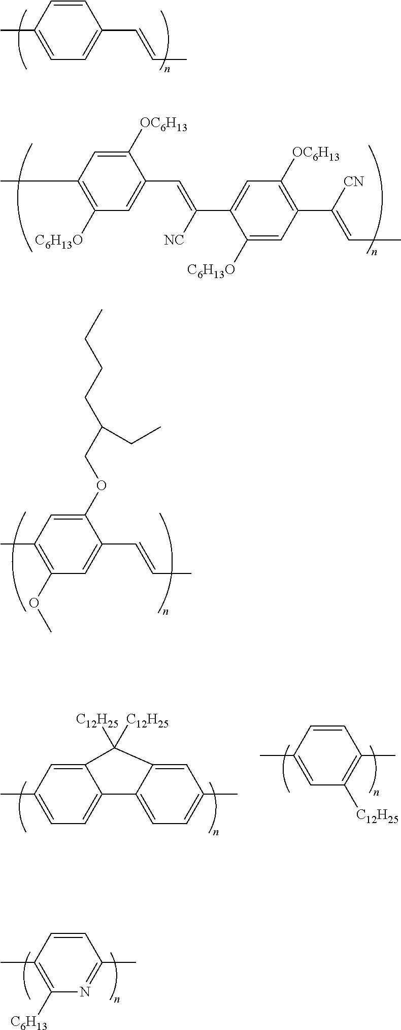
Polymer-Based Hole Transporting Compound

Polymer-Based Light Emitting Compound
An anode material used in the organic light emitting device of the present invention preferably has as large a work function as possible. Examples of the anode material that can be used include: metal elements such as gold, silver, platinum, nickel, palladium, cobalt, selenium, and vanadium, and alloys thereof obtained by combining the multiple metal elements; and metal oxides such as tin oxide, zinc oxide, indium tin oxide (ITO), and indium zinc oxide. A conductive polymer such as polyaniline, polypyrrole, polythiophene, and polyphenylene sulfide can also be used. Each of those electrode substances may be used alone, or a plurality of the substances may be used in combination.
On the other hand, the cathode material preferably has as small a work function as possible. Examples of the cathode material that can be used include metal elements such as lithium, sodium, potassium, cesium, calcium, magnesium, aluminum, indium, silver, lead, tin, and chromium, alloys obtained by combining the multiple metal elements, and salts of those metal elements. A metal oxide such as indium tin oxide (ITO) can also be used. In addition, a cathode may have a single layer constitution or a multilayer constitution.
A substrate to be used in the organic light emitting device of the present invention is not particularly limited; provided that an opaque substrate such as a metallic substrate or a ceramic substrate, or a transparent substrate such as glass, quartz, or a plastic sheet is used. In addition, a luminescent color can also be controlled by using a color filter film, a fluorescent color conversion filter film, a dielectric reflective film, or the like as the substrate.
The produced device may be provided with a protective layer or a sealing layer for the purpose of preventing the device from contacting with oxygen, moisture, or the like. Examples of the protective layer include: inorganic material films such as a diamond thin film, a metal oxide, and a metal nitride; polymer films such as a fluorine resin, polyparaxylene, polyethylene, a silicone resin, and a polystyrene resin; and a photocurable resin. In addition, the device itself can be covered with glass, a gas impervious film, metal, or the like, and can be packaged with an appropriate sealing resin.
It is preferred that the light emitting layer of the present invention is produced by a solution coating method. Examples of the coating method include spin coating, dispensing, printing, slit coating, an ink jet method, and spraying. The thickness of the light emitting layer is determined in view of the emission start voltage and the application voltage of the organic light emitting device, and is less than 10 μm, preferably 1 μm or less, and more preferably 30 nm or more to 500 nm or less.
The organic light emitting device of the present invention may have a plurality of organic layers in addition to the light emitting layer, and examples of the organic layers include a hole injecting layer, a hole transporting layer, a hole/exciton blocking layer, an electron transporting layer, and an electron injecting layer. These layers are produced by vapor deposition or solution coating, and the thickness thereof is less than 5 μm, preferably 1 μm or less, and more preferably 10 nm or more to 500 nm or less.
Next, the display apparatus of the present invention will be described.
The case where the above organic light emitting device is used in a display will be described. FIG. 11 schematically illustrates the state in which the organic light emitting device and the circuit illustrated in FIGS. 9 and 10 provided as one pixel are arranged two-dimensionally in a plural number on an identical plane, i.e., the arrangement in a matrix. The pixels are connected to a gate driver and a source driver via wiring, and supplied with a driving pulse, whereby the pixels are placed in an emission state or a non-emission state. A region in which a plurality of such organic light emitting devices are placed as pixels in the identical plane in an in-plane direction corresponds to a display region. That is, the organic light emitting device of the present embodiment can be used in the display region.
The display may have any form, as long as it is a display apparatus for a television or a personal computer, or an appliance having a portion displaying an image. For example, the display may be a portable display apparatus. Alternatively, the display according to the present embodiment can be used in a display portion of an electron imaging apparatus such as a digital camera and a mobile telephone.
Hereinafter, the present invention will be described more specifically by way of examples. It should be noted that the present invention is not limited thereto.
An organic light emitting device illustrated in FIG. 8 was produced as follows.
Indium tin oxide (ITO) was formed into a film on a glass substrate (substrate 1) by sputtering, whereby an anode 2 was formed. At this time, the thickness of the anode 2 was set to be 120 nm. Then, the substrate with the ITO formed thereon was washed with an ultrasonic wave successively with acetone and isopropyl alcohol (IPA), and washed by boiling with IPA, followed by drying. The substrate was further washed with UV/ozone. The substrate treated as described above was used as a transparent conductive support substrate.
Next, Baytron P A1-4083 (manufactured by H.C. Starck Inc.) was formed into a film on the transparent conductive support substrate by spin coating. At this time, the thickness of Bytron was set to be 50 nm. Next, the resultant film was heated at 100° C. for 30 minutes, whereby a hole injecting layer 7 was formed.
Next, 0.5 g of a fluorene compound represented by the following formula and 0.5 g of poly(octafluoropentyl acrylate) (n=1.38, molecular weight: 15,000) were dissolved in 50 g of 1,2-dichloropropane to prepare a mixed solution. The mixed solution was applied to the hole injecting layer 7 by spin coating, and heated at 100° C. for one hour, whereby a light emitting layer 3 was formed. At this time, the thickness of the light emitting layer 3 was set to be 100 nm.
(Fluorene Compound)

Next, calcium was vapor-deposited on the light emitting layer 3 by vacuum vapor deposition, whereby a metal layer film was formed as an electron injecting layer 8. At this time, the film thickness of the electron injecting layer 8 was set to be 1 nm, the vacuum degree during vapor deposition was set to be 1.0 ×10⁻⁴ Pa, and the film forming rate was set to be 0.1 nm/sec.
Next, aluminum was vapor-deposited by vacuum vapor deposition, whereby a cathode 4 was formed. At this time, the film thickness of the cathode 4 was set to be 150 nm, the vacuum degree during vapor deposition was set to be 1.0×10⁻⁴ Pa, and the film forming rate was set to be 1.0 nm/sec. to 1.2 nm/sec.
Next, a glass plate for protection was placed over the cathode 4 in a nitrogen atmosphere, and sealed with an acrylic resin based adhesive. Thus, an organic light emitting device was obtained.
When a DC voltage of 5 V was applied to the obtained organic light emitting device, with the ITO electrode (anode 2) being a positive electrode and the A1 electrode (cathode 4) being a negative electrode, a current flowed through the device. The current density at this time was 20 mA/cm2. Further, in the device, blue light emission with a luminance of 1,200 cd/m2 was observed, the chromaticity of the EL light emission was (X, Y)=(0.14, 0.13), and the external quantum efficiency was 5.9%.
Further, when a voltage was applied for 100 hours while the current density was kept at 5.0 mA/cm2, the luminance changed from 250 cd/M2 (initial luminance) to 200 cd/m2 (after 100 hours). It was found from the result that the degradation in luminance of the organic light emitting device of the present example was small.
On the other hand, the refractive index of the light emitting layer 3 was measured with a spectral ellipsometer (GES 500 manufactured by SOPRA), or the like. As a sample for refractive index measurement, a glass plate with a film formed thereon separately by the same method as that of the light emitting layer 3 was used. As a result of the measurement, the refractive index of the light emitting layer 3 was 1.51. Table 1 shows the results.
In Example 1, as a material constituting the light emitting layer 3, poly(nonafluoropentyl acrylate) (n=1.36, molecular weight: 12,000) was used in place of poly(octafluoropentyl acrylate) (n=1.38, molecular weight: 15,000). A device was produced by the same method as that of Example 1 except for the above. The obtained device was evaluated in the same way as in Example 1. Further, the refractive index of the light emitting layer 3 was evaluated in the same way as in Example 1. Table 1 shows the results.
In Example 1, as a material constituting the light emitting layer 3, poly(trifluoroethyl acrylate) (n =1.41, molecular weight: 20,000) was used in place of poly(octafluoropentyl acrylate) (n=1.38, molecular weight: 15,000). A device was produced by the same method as that of Example 1 except for the above. The obtained device was evaluated in the same way as in Example 1. Further, the refractive index of the light emitting layer 3 was evaluated in the same way as in Example 1. Table 1 shows the results.
In Example 1, as a material constituting the light emitting layer 3, poly(trifluoroethyl methacrylate) (n=1.44, molecular weight: 25,000) was used in place of poly(octafluoropentyl acrylate) (n=1.38, molecular weight: 15,000). A device was produced by the same method as that of Example 1 except for the above. The obtained device was evaluated in the same way as in Example 1. Further, the refractive index of the light emitting layer 3 was evaluated in the same way as in Example 1. Table 1 shows the results.
In Example 1, as a material constituting the light emitting layer 3, poly(oxypropylene) (n=1.45, molecular weight: 15,000) was used in place of poly(octafluoropentyl acrylate) (n=1.38, molecular weight: 15,000). A device was produced by the same method as that of Example 1 except for the above. The obtained device was evaluated in the same way as in Example 1. Further, the refractive index of the light emitting layer 3 was evaluated in the same way as in Example 1. Table 1 shows the results.
In Example 1, as a material constituting the light emitting layer 3, poly(vinyl isobutyl ether) (n=1.45, molecular weight: 25,000) was used in place of poly(octafluoropentyl acrylate) (n=1.38, molecular weight: 15,000). A device was produced by the same method as that of Example 1 except for the above. The obtained device was evaluated in the same way as in Example 1. Further, the refractive index of the light emitting layer 3 was evaluated in the same way as in Example 1. Table 1 shows the results.
In Example 1, as a material constituting the light emitting layer 3, poly(vinyl octyl ether) (n=1.46, molecular weight: 20,000) was used in place of poly(octafluoropentyl acrylate) (n=1.38, molecular weight: 15,000). A device was produced by the same method as that of Example 1 except for the above. The obtained device was evaluated in the same way as in Example 1. Further, the refractive index of the light emitting layer 3 was evaluated in the same way as in Example 1. Table 1 shows the results.
In Example 1, as a material constituting the light emitting layer 3, poly(vinyl propionate) (n=1.47, molecular weight: 15,000) was used in place of poly(octafluoropentyl acrylate) (n=1.38, molecular weight: 15,000). A device was produced by the same method as that of Example 1 except for the above. The obtained device was evaluated in the same way as in Example 1. Further, the refractive index of the light emitting layer 3 was evaluated in the same way as in Example 1. Table 1 shows the results.
In Example 1, as a material constituting the light emitting layer 3, poly(methyl methacrylate) (n=1.49, molecular weight: 15,000) was used in place of poly(octafluoropentyl acrylate) (n=1.38, molecular weight: 15,000). A device was produced by the same method as that of Example 1 except for the above. The obtained device was evaluated in the same way as in Example 1. Further, the refractive index of the light emitting layer 3 was evaluated in the same way as in Example 1. Table 1 shows the results.
In Example 1, as a material constituting the light emitting layer 3, polycarbonate Z200 (manufactured by MITSUBISHI GAS CHEMICAL COMPANY, INC.) was used in place of poly(octafluoropentyl acrylate) (n=1.38, molecular weight: 15,000). A device was produced by the same method as that of Example 1 except for the above. The obtained device was evaluated in the same way as in Example 1. Further, the refractive index of the light emitting layer 3 was evaluated in the same way as in Example 1. Table 1 shows the results.
| TABLE 1 | ||||||
| Refractive | ||||||
| index of | External | Change in luminance | ||||
| Refractive | light | Initial luminance | quantum | (initial luminance → | ||
| index of | emitting | @5 v application | efficiency | after 100 hours) | ||
| polymer | layer | (current density) | (%) | @5 mA/m2 | ||
| Example 1 | 1.38 | 1.51 | 1200 cd/m2 | 5.9 | 250 → 200 cd/m2 |
| (20 mA/m2) | |||||
| Example 2 | 1.36 | 1.48 | 1100 cd/m2 | 6.3 | 240 → 200 cd/m2 |
| (18 mA/m2) | |||||
| Example 3 | 1.41 | 1.54 | 1200 cd/m2 | 5.2 | 220 → 180 cd/m2 |
| (22 mA/m2) | |||||
| Example 4 | 1.44 | 1.56 | 1000 cd/m2 | 4.8 | 210 → 150 cd/m2 |
| (18 mA/m2) | |||||
| Example 5 | 1.45 | 1.57 | 1200 cd/m2 | 4.7 | 200 → 170 cd/m2 |
| (24 mA/m2) | |||||
| Example 6 | 1.45 | 1.57 | 1200 cd/m2 | 4.7 | 220 → 180 cd/m2 |
| (24 mA/m2) | |||||
| Example 7 | 1.46 | 1.58 | 1000 cd/m2 | 4.6 | 200 → 160 cd/m2 |
| (22 mA/m2) | |||||
| Example 8 | 1.47 | 1.59 | 1000 cd/m2 | 4.6 | 210 → 180 cd/m2 |
| (22 mA/m2) | |||||
| Comparative | 1.49 | 1.62 | 700 cd/m2 | 3.5 | 150 → 70 cd/m2 |
| Example 1 | (20 mA/m2) | ||||
| Comparative | 1.72 | 1.72 | 800 cd/m2 | 3.1 | 170 → 60 cd/m2 |
| Example 2 | (22 mA/m2) | ||||
An organic light emitting device illustrated in FIG. 8 was produced as follows.
First, a transparent conductive support substrate was produced by the same method as that of Example 1, and the hole injecting layer 7 was formed on the transparent conductive support substrate by the same method as that of Example 1.
Next, 0.3 g of a fluorene compound represented by the following formula, 0.03 g of Ir complex represented by the following formula, and 0.5 g of poly(octafluoropentyl acrylate) (n=1.38, molecular weight: 15,000) were dissolved in 50 g of 1,2-dichloropropane to prepare a mixed solution. The mixed solution was applied to the above hole injecting layer 7 by spin coating, and heated at 100° C. for 1 hour, whereby a light emitting layer 3 was formed. At this time, the film thickness of the light emitting layer 3 was set to be 100 nm.
(Fluorene Compound) and (Ir Complex)

Next, calcium was vapor-deposited on the light emitting layer 3 by vacuum vapor deposition, whereby a metal layer film was formed as an electron injecting layer 8. The film thickness of the electron injecting layer 8 was set to be 1 nm, the vacuum degree during vapor deposition was set to be 1.0×10⁻⁴ Pa, and the film forming rate was set to be 0.1 nm/sec.
Next, aluminum was vapor-deposited by vacuum vapor deposition, whereby a cathode 4 was formed. At this time, the film thickness of the cathode 4 was set to be 150 nm, the vacuum degree during vapor deposition was set to be 1.0×10⁻⁴ Pa, and the film forming rate was set to be 1.0 nm/sec. to 1.2 nm/sec.
Next, a glass plate for protection was placed over the cathode 4 in a nitrogen atmosphere, and sealed with an acrylic resin based adhesive. Thus, an organic light emitting device was obtained.
When a DC voltage of 5 V was applied to the obtained organic light emitting device, with the ITO electrode (anode 2) being a positive electrode and the A1 electrode (cathode 4) being a negative electrode, a current flowed through the device. The current density at this time was 20 mA/cm2. Further, in the device, red light emission with a luminance of 2,800 cd/m2 was observed, the chromaticity of the EL light emission was (X, Y)=(0.67, 0.32), and the external quantum efficiency was 15%.
Further, when a voltage was applied for 100 hours while the current density was kept at 5.0 mA/cm2, the luminance changed from 450 cd/m2 (initial luminance) to 340 cd/m2 (after 100 hours). It was found from the result that the degradation in luminance of the organic light emitting device of the present example was small. On the other hand, the refractive index of the light emitting layer 3 was measured to be 1.50 by the same method as that in Example 1. Table 2 shows the results.
In Example 9, as a material constituting the light emitting layer 3, poly(nonafluoropentyl acrylate) (n=1.36, molecular weight: 12,000) was used in place of poly(octafluoropentyl acrylate) (n=1.38, molecular weight: 15,000). A device was produced by the same method as that of Example 9 except for the above. The obtained device was evaluated in the same way as in Example 9. Further, the refractive index of the light emitting layer 3 was evaluated in the same way as in Example 9. Table 2 shows the results.
In Example 9, as a material constituting the light emitting layer 3, poly(oxypropylene) (n=1.45, molecular weight: 15,000) was used in place of poly(octafluoropentyl acrylate) (n=1.38, molecular weight: 15,000). A device was produced by the same method as that of Example 9 except for the above. The obtained device was evaluated in the same way as in Example 9. Further, the refractive index of the light emitting layer 3 was evaluated in the same way as in Example 9. Table 2 shows the results.
In Example 9, as a material constituting the light emitting layer 3, poly(vinyl octyl ether) (n=1.46, molecular weight: 20,000) was used in place of poly(octafluoropentyl acrylate) (n=1.38, molecular weight: 15,000). A device was produced by the same method as that of Example 9 except for the above. The obtained device was evaluated in the same way as in Example 9. Further, the refractive index of the light emitting layer 3 was evaluated in the same way as in Example 9. Table 2 shows the results.
In Example 9, as a material constituting the light emitting layer 3, poly(vinyl propionate) (n=1.47, molecular weight: 15,000) was used in place of poly(octafluoropentyl acrylate) (n=1.38, molecular weight: 15,000). A device was produced by the same method as that of Example 9 except for the above. The obtained device was evaluated in the same way as in Example 9. Further, the refractive index of the light emitting layer 3 was evaluated in the same way as in Example 9. Table 2 shows the results.
In Example 9, as a material constituting the light emitting layer 3, poly(methyl methacrylate) (n=1.49, molecular weight: 15,000) was used in place of poly(octafluoropentyl acrylate) (n=1.38, molecular weight: 15,000). A device was produced by the same method as that of Example 9 except for the above. The obtained device was evaluated in the same way as in Example 9. Further, the refractive index of the light emitting layer 3 was evaluated in the same way as in Example 9. Table 2 shows the results.
In Example 9, as a material constituting the light emitting layer 3, polycarbonate Z200 (manufactured by MITSUBISHI GAS CHEMICAL COMPANY, INC.) was used in place of poly(octafluoropentyl acrylate) (n=1.38, molecular weight: 15,000). A device was produced by the same method as that of Example 9 except for the above. The obtained device was evaluated in the same way as in Example 9. Further, the refractive index of the light emitting layer 3 was evaluated in the same way as in Example 9. Table 2 shows the results.
| TABLE 2 | ||||||
| Refractive | ||||||
| index of | External | Change in luminance | ||||
| Refractive | light | Initial luminance | quantum | (initial luminance → | ||
| index of | emitting | @5 v application | efficiency | after 100 hours) | ||
| polymer | layer | (current density) | (%) | @5 mA/m2 | ||
| Example 9 | 1.38 | 1.50 | 2800 cd/m2 | 15 | 450 → 340 cd/m2 |
| (20 mA/m2) | |||||
| Example | 1.36 | 1.47 | 3000 cd/m2 | 17 | 520 → 430 cd/m2 |
| 10 | (18 mA/m2) | ||||
| Example | 1.45 | 1.55 | 2400 cd/ |
13 | 400 → 300 cd/m2 |
| 11 | (18 mA/m2) | ||||
| Example | 1.46 | 1.57 | 2500 cd/ |
12 | 400 → 320 cd/m2 |
| 12 | (20 mA/m2) | ||||
| Example | 1.47 | 1.57 | 2200 cd/ |
12 | 380 → 300 cd/m2 |
| 13 | (18 mA/m2) | ||||
| Comparative | 1.49 | 1.61 | 1800 cd/ |
8 | 350 → 200 cd/m2 |
| Example 3 | (22 mA/m2) | ||||
| Comparative | 1.72 | 1.72 | 1500 cd/ |
6 | 270 → 100 cd/m2 |
| Example 4 | (24 mA/m2) | ||||
As described above, according to the present invention, an organic light emitting device with a high light extraction efficiency, a high light emitting efficiency, and high durability can be realized. Further, a display apparatus with the above organic light emitting device can be provided.
While the present invention has been described with reference to exemplary embodiments, it is to be understood that the invention is not limited to the disclosed exemplary embodiments. The scope of the following claims is to be accorded the broadest interpretation so as to encompass all such modifications and equivalent structures and functions.
This application claims the benefit of Japanese Patent Application No. 2007-167194, filed Jun. 26, 2007, which is hereby incorporated by reference herein in its entirety.
Claims (6)
1. An organic light emitting device comprising:
an anode;
a cathode; and
a light emitting layer formed of an organic compound arranged between the anode and the cathode,
wherein the light emitting layer comprises at least one organic light emitting material and an aliphatic compound not having an aromatic ring, and a refractive index of the light emitting layer is 1.40 or more to 1.60 or less.
2. The organic light emitting device according to claim 1 , wherein the organic light emitting material is either one of a fluorescent material and a phosphorescent material.
3. The organic light emitting device according to claim 1 , wherein an amount of the organic light emitting material is 2 parts by weight or more to 150 parts by weight or less with respect to 100 parts by weight of the aliphatic compound.
4. A display apparatus comprising the organic light emitting device according to claim 1 .
5. The organic light emitting device according to claim 1 , wherein the aliphatic compound is at least one selected from the group consisting of poly(undecafluorohexyl acrylate), poly(nonafluoropentyl acrylate), poly(pentafluorovinyl propionate), poly(heptafluorobutyl acrylate), poly(trifluorovinyl acetate), poly(octafluoropentyl acrylate), poly(pentafluoropropyl acrylate), poly(2,2,3,4,4,4-hexafluorobutyl acrylate), poly(trifluoroethyl acrylate), poly(trifluorochloroethylene) and poly(trifluoroethyl methacrylate).
6. The organic light emitting device according to claim 1 , wherein the aliphatic compound is at least one selected from the group consisting of poly(oxypropylene), poly(vinyl isobutyl ether), poly(vinyl ethyl ether), poly(oxyethylene), poly(vinyl pentyl ether), poly(vinyl octyl ether), poly(vinyl decyl ether), poly(vinyl dodecyl ether), poly(oxy-1-oxopentamethylene), poly(vinyl propionate) and poly(vinyl methyl ether).
Applications Claiming Priority (2)
| Application Number | Priority Date | Filing Date | Title |
|---|---|---|---|
| JP2007167194A JP5153227B2 (en) | 2007-06-26 | 2007-06-26 | Organic light emitting device |
| JP2007-167194 | 2007-06-26 |
Publications (2)
| Publication Number | Publication Date |
|---|---|
| US20090004507A1 US20090004507A1 (en) | 2009-01-01 |
| US8263235B2 true US8263235B2 (en) | 2012-09-11 |
Family
ID=40160943
Family Applications (1)
| Application Number | Title | Priority Date | Filing Date |
|---|---|---|---|
| US12/144,389 Expired - Fee Related US8263235B2 (en) | 2007-06-26 | 2008-06-23 | Organic light emitting device having a high light extraction efficiency |
Country Status (2)
| Country | Link |
|---|---|
| US (1) | US8263235B2 (en) |
| JP (1) | JP5153227B2 (en) |
Cited By (4)
| Publication number | Priority date | Publication date | Assignee | Title |
|---|---|---|---|---|
| WO2017040737A1 (en) | 2015-09-01 | 2017-03-09 | Promerus, Llc | Polycycloolefin polymer compositions as optical materials |
| WO2018129121A1 (en) | 2017-01-06 | 2018-07-12 | Promerus, Llc | Polycycloolefin polymer compositions as optical materials |
| WO2019032937A1 (en) | 2017-08-10 | 2019-02-14 | Promerus, Llc | Polycycloolefin polymer and inorganic nanoparticle compositions as optical materials |
| WO2019147878A1 (en) | 2018-01-26 | 2019-08-01 | Promerus, Llc | Polycycloolefin monomers and catalyst activated by compound capable of generating photoacid as optical materials |
Families Citing this family (2)
| Publication number | Priority date | Publication date | Assignee | Title |
|---|---|---|---|---|
| US10991915B2 (en) * | 2016-01-29 | 2021-04-27 | University Of Florida Research Foundation, Incorporated | Organic light-emitting diodes comprising grating structures and light extraction layers |
| US11738366B2 (en) | 2019-01-25 | 2023-08-29 | The Regents Of The University Of California | Method of coating an object |
Citations (15)
| Publication number | Priority date | Publication date | Assignee | Title |
|---|---|---|---|---|
| JPH07240277A (en) | 1994-02-25 | 1995-09-12 | Idemitsu Kosan Co Ltd | Organic electroluminescent element |
| JP2001202827A (en) | 1999-11-10 | 2001-07-27 | Matsushita Electric Works Ltd | Method of manufacturing transparent conductive substrate, light emission device, plane light emission plate and manufacturing method of plane light emission plate, plane fluorescent lamp, and plasma display |
| JP2002056980A (en) | 2000-08-10 | 2002-02-22 | Sharp Corp | Organic el layer coating fluid, organic el element and manufacturing method of the same |
| JP2003272841A (en) | 2002-03-18 | 2003-09-26 | Toshiba Corp | Organic el display device and manufacturing method of the same |
| US6762553B1 (en) | 1999-11-10 | 2004-07-13 | Matsushita Electric Works, Ltd. | Substrate for light emitting device, light emitting device and process for production of light emitting device |
| US6768132B2 (en) * | 2002-03-07 | 2004-07-27 | 3M Innovative Properties Company | Surface modified organic thin film transistors |
| US20050048313A1 (en) * | 2003-08-29 | 2005-03-03 | Fujitsu Limited | Fluorescent material, organic electroluminescent element and organic electroluminescent display |
| US20050225232A1 (en) * | 2004-04-07 | 2005-10-13 | Eastman Kodak Company | Color OLED with added color gamut pixels |
| US20060017376A1 (en) | 2004-07-20 | 2006-01-26 | Canon Kabushiki Kaisha | Organic light emitting device |
| US7034454B2 (en) | 2002-12-16 | 2006-04-25 | Canon Kabushiki Kaisha | Organic light emitting device with reverse intersystem crossing light emitting molecules |
| US20060102913A1 (en) * | 2004-11-17 | 2006-05-18 | Joon-Young Park | Full color OLED and method of fabricating the same |
| US20060163562A1 (en) * | 2003-07-07 | 2006-07-27 | Koninklijke Philips Electronics N.V. | Multifluorinated conductor material for leds for improving the light outcoupling |
| US7309533B2 (en) | 2003-06-27 | 2007-12-18 | Canon Kabushiki Kaisha | Substituted anthryl derivative and electroluminescence device using the same |
| US20100320446A1 (en) * | 2007-02-05 | 2010-12-23 | Lg Chem, Ltd. | Organic light-emitting device having improved light-emitting efficiency and method for fabricating the same |
| US7991257B1 (en) * | 2007-05-16 | 2011-08-02 | Fusion Optix, Inc. | Method of manufacturing an optical composite |
Family Cites Families (1)
| Publication number | Priority date | Publication date | Assignee | Title |
|---|---|---|---|---|
| JP2007141736A (en) * | 2005-11-21 | 2007-06-07 | Fujifilm Corp | Organic electroluminescent element |
-
2007
- 2007-06-26 JP JP2007167194A patent/JP5153227B2/en not_active Expired - Fee Related
-
2008
- 2008-06-23 US US12/144,389 patent/US8263235B2/en not_active Expired - Fee Related
Patent Citations (18)
| Publication number | Priority date | Publication date | Assignee | Title |
|---|---|---|---|---|
| US5891554A (en) | 1994-02-25 | 1999-04-06 | Idemitsu Kosan Co., Ltd. | Organic electroluminescence device |
| US6124024A (en) | 1994-02-25 | 2000-09-26 | Idemitsu Kosan Co., Ltd. | Organic electroluminescence device |
| JPH07240277A (en) | 1994-02-25 | 1995-09-12 | Idemitsu Kosan Co Ltd | Organic electroluminescent element |
| JP2001202827A (en) | 1999-11-10 | 2001-07-27 | Matsushita Electric Works Ltd | Method of manufacturing transparent conductive substrate, light emission device, plane light emission plate and manufacturing method of plane light emission plate, plane fluorescent lamp, and plasma display |
| US6762553B1 (en) | 1999-11-10 | 2004-07-13 | Matsushita Electric Works, Ltd. | Substrate for light emitting device, light emitting device and process for production of light emitting device |
| JP2002056980A (en) | 2000-08-10 | 2002-02-22 | Sharp Corp | Organic el layer coating fluid, organic el element and manufacturing method of the same |
| US6768132B2 (en) * | 2002-03-07 | 2004-07-27 | 3M Innovative Properties Company | Surface modified organic thin film transistors |
| US6908696B2 (en) | 2002-03-18 | 2005-06-21 | Kabushiki Kaisha Toshiba | Organic electro luminescence display device |
| JP2003272841A (en) | 2002-03-18 | 2003-09-26 | Toshiba Corp | Organic el display device and manufacturing method of the same |
| US7034454B2 (en) | 2002-12-16 | 2006-04-25 | Canon Kabushiki Kaisha | Organic light emitting device with reverse intersystem crossing light emitting molecules |
| US7309533B2 (en) | 2003-06-27 | 2007-12-18 | Canon Kabushiki Kaisha | Substituted anthryl derivative and electroluminescence device using the same |
| US20060163562A1 (en) * | 2003-07-07 | 2006-07-27 | Koninklijke Philips Electronics N.V. | Multifluorinated conductor material for leds for improving the light outcoupling |
| US20050048313A1 (en) * | 2003-08-29 | 2005-03-03 | Fujitsu Limited | Fluorescent material, organic electroluminescent element and organic electroluminescent display |
| US20050225232A1 (en) * | 2004-04-07 | 2005-10-13 | Eastman Kodak Company | Color OLED with added color gamut pixels |
| US20060017376A1 (en) | 2004-07-20 | 2006-01-26 | Canon Kabushiki Kaisha | Organic light emitting device |
| US20060102913A1 (en) * | 2004-11-17 | 2006-05-18 | Joon-Young Park | Full color OLED and method of fabricating the same |
| US20100320446A1 (en) * | 2007-02-05 | 2010-12-23 | Lg Chem, Ltd. | Organic light-emitting device having improved light-emitting efficiency and method for fabricating the same |
| US7991257B1 (en) * | 2007-05-16 | 2011-08-02 | Fusion Optix, Inc. | Method of manufacturing an optical composite |
Non-Patent Citations (1)
| Title |
|---|
| Arentoft et al., "Second-harmonic Imaging of Poled Silica Waveguides," Appl. Phys. Ltrs., vol. 76, No. 1, 25-27 (2000). |
Cited By (4)
| Publication number | Priority date | Publication date | Assignee | Title |
|---|---|---|---|---|
| WO2017040737A1 (en) | 2015-09-01 | 2017-03-09 | Promerus, Llc | Polycycloolefin polymer compositions as optical materials |
| WO2018129121A1 (en) | 2017-01-06 | 2018-07-12 | Promerus, Llc | Polycycloolefin polymer compositions as optical materials |
| WO2019032937A1 (en) | 2017-08-10 | 2019-02-14 | Promerus, Llc | Polycycloolefin polymer and inorganic nanoparticle compositions as optical materials |
| WO2019147878A1 (en) | 2018-01-26 | 2019-08-01 | Promerus, Llc | Polycycloolefin monomers and catalyst activated by compound capable of generating photoacid as optical materials |
Also Published As
| Publication number | Publication date |
|---|---|
| US20090004507A1 (en) | 2009-01-01 |
| JP2009009975A (en) | 2009-01-15 |
| JP5153227B2 (en) | 2013-02-27 |
Similar Documents
| Publication | Publication Date | Title |
|---|---|---|
| US7919195B2 (en) | System for displaying images | |
| KR101933266B1 (en) | Display unit and electronic apparatus | |
| KR101064607B1 (en) | Organic semiconductor device and method for manufacturing the same | |
| US7301277B2 (en) | Electro-optical apparatus, manufacturing method thereof, and electronic instrument | |
| JP4450207B2 (en) | Method for manufacturing light emitting device | |
| US9240569B2 (en) | Display and electronic system | |
| US8263235B2 (en) | Organic light emitting device having a high light extraction efficiency | |
| JP4548121B2 (en) | Method for manufacturing light emitting device | |
| JP2013045522A (en) | Display device and manufacturing method therefor | |
| JP4305425B2 (en) | Electronic devices and electronic equipment | |
| JP2019192557A (en) | Organic el element, and display device, imaging apparatus, lighting device, and moving body having the same | |
| JP4277816B2 (en) | LIGHT EMITTING ELEMENT, DISPLAY DEVICE, AND ELECTRONIC DEVICE | |
| JP4534875B2 (en) | LIGHT EMITTING ELEMENT, LIGHT EMITTING ELEMENT MANUFACTURING METHOD, ELECTRONIC DEVICE, AND ELECTRONIC DEVICE | |
| US20080024059A1 (en) | System for displaying images incluidng electroluminescent device and method for fabricating the same | |
| JPWO2018168225A1 (en) | Composition for producing electronic device, method for producing composition for producing electronic device, organic thin film, and method for producing organic thin film | |
| JP4609135B2 (en) | Method for manufacturing organic electroluminescence element | |
| JP2019192556A (en) | Organic el element, and display device, lighting device, and moving body having the same | |
| JP5164354B2 (en) | Organic EL device | |
| JP4311380B2 (en) | Electronic device substrate, method for manufacturing electronic device substrate, electronic device and electronic apparatus | |
| JP4715329B2 (en) | Manufacturing method of substrate for electronic device | |
| JP4730133B2 (en) | Organic EL device and electronic device | |
| JP2005183147A (en) | Organic electroluminescence display device | |
| CN116806447A (en) | Display device and manufacturing method of display device | |
| JP2009199905A (en) | Organic light-emitting device and electron equipment |
Legal Events
| Date | Code | Title | Description |
|---|---|---|---|
| AS | Assignment |
Owner name: CANON KABUSHIKI KAISHA, JAPAN Free format text: ASSIGNMENT OF ASSIGNORS INTEREST;ASSIGNOR:SUZUKI, KOICHI;REEL/FRAME:021228/0499 Effective date: 20080616 |
|
| FEPP | Fee payment procedure |
Free format text: PAYOR NUMBER ASSIGNED (ORIGINAL EVENT CODE: ASPN); ENTITY STATUS OF PATENT OWNER: LARGE ENTITY |
|
| REMI | Maintenance fee reminder mailed | ||
| LAPS | Lapse for failure to pay maintenance fees | ||
| STCH | Information on status: patent discontinuation |
Free format text: PATENT EXPIRED DUE TO NONPAYMENT OF MAINTENANCE FEES UNDER 37 CFR 1.362 |
|
| FP | Lapsed due to failure to pay maintenance fee |
Effective date: 20160911 |