US8304512B2 - Benzodithiophene based materials compositions - Google Patents
Benzodithiophene based materials compositions Download PDFInfo
- Publication number
- US8304512B2 US8304512B2 US12/689,613 US68961310A US8304512B2 US 8304512 B2 US8304512 B2 US 8304512B2 US 68961310 A US68961310 A US 68961310A US 8304512 B2 US8304512 B2 US 8304512B2
- Authority
- US
- United States
- Prior art keywords
- group
- electron acceptor
- polymer
- polymer semiconductor
- aromatic
- Prior art date
- Legal status (The legal status is an assumption and is not a legal conclusion. Google has not performed a legal analysis and makes no representation as to the accuracy of the status listed.)
- Active
Links
- 0 [1*]C1=C2SC(C(C)(C)C)=CC2=C([2*])C2=C1C=C(C(C)(C)C)S2 Chemical compound [1*]C1=C2SC(C(C)(C)C)=CC2=C([2*])C2=C1C=C(C(C)(C)C)S2 0.000 description 17
- ZYRJFCPKECVVRO-UHFFFAOYSA-N CC(C)(C)C1=C2N=C3C(=NC2=C(C(C)(C)C)S1)/C1=C/C=C\C2=CC=CC3=C21.CC(C)(C)C1=C2N=C3C(=NC2=C(C(C)(C)C)S1)C1=C(C=CC=C1)C1=C3C=CC=C1.CC(C)(C)C1=C[Y]=C(C(C)(C)C)C2=NCN=C12.CC(C)(C)C1=C[Y]=C(C(C)(C)C)C2=NCN=C12 Chemical compound CC(C)(C)C1=C2N=C3C(=NC2=C(C(C)(C)C)S1)/C1=C/C=C\C2=CC=CC3=C21.CC(C)(C)C1=C2N=C3C(=NC2=C(C(C)(C)C)S1)C1=C(C=CC=C1)C1=C3C=CC=C1.CC(C)(C)C1=C[Y]=C(C(C)(C)C)C2=NCN=C12.CC(C)(C)C1=C[Y]=C(C(C)(C)C)C2=NCN=C12 ZYRJFCPKECVVRO-UHFFFAOYSA-N 0.000 description 3
- YGRSRAYLCGUTFV-UXRMLUQQSA-N C1=CC2=CC3=C(C=CS3)C=C2S1.[2H]B[3H] Chemical compound C1=CC2=CC3=C(C=CS3)C=C2S1.[2H]B[3H] YGRSRAYLCGUTFV-UXRMLUQQSA-N 0.000 description 1
- HFOJYFVLCSKUBD-UHFFFAOYSA-N CC#CCCCCCCCCCC.CCCCCCCCCCC#CC1=C2C=CSC2=C(C#CCCCCCCCCCC)C2=C1SC=C2.CCCCCCCCCCCCC1=C2C=CSC2=C(CCCCCCCCCCCC)C2=C1SC=C2.O=C1C2=C(SC=C2)C(=O)C2=C1SC=C2 Chemical compound CC#CCCCCCCCCCC.CCCCCCCCCCC#CC1=C2C=CSC2=C(C#CCCCCCCCCCC)C2=C1SC=C2.CCCCCCCCCCCCC1=C2C=CSC2=C(CCCCCCCCCCCC)C2=C1SC=C2.O=C1C2=C(SC=C2)C(=O)C2=C1SC=C2 HFOJYFVLCSKUBD-UHFFFAOYSA-N 0.000 description 1
- OUGYXKMSQKGVLK-UHFFFAOYSA-N CC1(C)OB(C2=CC=C(B3OC(C)(C)C(C)(C)O3)C3=NSN=C23)OC1(C)C.CCCCCCCCCCCCC1=C2C=C(Br)SC2=C(CCCCCCCCCCCC)C2=C1SC(Br)=C2.CCCCCCCCCCCCC1=C2C=C(C)SC2=C(CCCCCCCCCCCC)C2=C1SC(C1=CC=C(C)C3=NSN=C13)=C2.P Chemical compound CC1(C)OB(C2=CC=C(B3OC(C)(C)C(C)(C)O3)C3=NSN=C23)OC1(C)C.CCCCCCCCCCCCC1=C2C=C(Br)SC2=C(CCCCCCCCCCCC)C2=C1SC(Br)=C2.CCCCCCCCCCCCC1=C2C=C(C)SC2=C(CCCCCCCCCCCC)C2=C1SC(C1=CC=C(C)C3=NSN=C13)=C2.P OUGYXKMSQKGVLK-UHFFFAOYSA-N 0.000 description 1
- XJHGOZMTTDWXAD-UHFFFAOYSA-N CCCCCCCCCCCCC.CCCCCCCCCCCCC1=C2C=CSC2=C(CCCCCCCCCCCC)C2=C1SC=C2.O=C1C2=C(SC=C2)C(=O)C2=C1SC=C2 Chemical compound CCCCCCCCCCCCC.CCCCCCCCCCCCC1=C2C=CSC2=C(CCCCCCCCCCCC)C2=C1SC=C2.O=C1C2=C(SC=C2)C(=O)C2=C1SC=C2 XJHGOZMTTDWXAD-UHFFFAOYSA-N 0.000 description 1
Images


Classifications
-
- C—CHEMISTRY; METALLURGY
- C08—ORGANIC MACROMOLECULAR COMPOUNDS; THEIR PREPARATION OR CHEMICAL WORKING-UP; COMPOSITIONS BASED THEREON
- C08G—MACROMOLECULAR COMPOUNDS OBTAINED OTHERWISE THAN BY REACTIONS ONLY INVOLVING UNSATURATED CARBON-TO-CARBON BONDS
- C08G61/00—Macromolecular compounds obtained by reactions forming a carbon-to-carbon link in the main chain of the macromolecule
- C08G61/12—Macromolecular compounds containing atoms other than carbon in the main chain of the macromolecule
- C08G61/122—Macromolecular compounds containing atoms other than carbon in the main chain of the macromolecule derived from five- or six-membered heterocyclic compounds, other than imides
- C08G61/123—Macromolecular compounds containing atoms other than carbon in the main chain of the macromolecule derived from five- or six-membered heterocyclic compounds, other than imides derived from five-membered heterocyclic compounds
- C08G61/126—Macromolecular compounds containing atoms other than carbon in the main chain of the macromolecule derived from five- or six-membered heterocyclic compounds, other than imides derived from five-membered heterocyclic compounds with a five-membered ring containing one sulfur atom in the ring
-
- C—CHEMISTRY; METALLURGY
- C08—ORGANIC MACROMOLECULAR COMPOUNDS; THEIR PREPARATION OR CHEMICAL WORKING-UP; COMPOSITIONS BASED THEREON
- C08G—MACROMOLECULAR COMPOUNDS OBTAINED OTHERWISE THAN BY REACTIONS ONLY INVOLVING UNSATURATED CARBON-TO-CARBON BONDS
- C08G75/00—Macromolecular compounds obtained by reactions forming a linkage containing sulfur with or without nitrogen, oxygen, or carbon in the main chain of the macromolecule
- C08G75/02—Polythioethers
- C08G75/0204—Polyarylenethioethers
- C08G75/0227—Polyarylenethioethers derived from monomers containing two or more aromatic rings
-
- C—CHEMISTRY; METALLURGY
- C08—ORGANIC MACROMOLECULAR COMPOUNDS; THEIR PREPARATION OR CHEMICAL WORKING-UP; COMPOSITIONS BASED THEREON
- C08L—COMPOSITIONS OF MACROMOLECULAR COMPOUNDS
- C08L65/00—Compositions of macromolecular compounds obtained by reactions forming a carbon-to-carbon link in the main chain; Compositions of derivatives of such polymers
-
- H—ELECTRICITY
- H10—SEMICONDUCTOR DEVICES; ELECTRIC SOLID-STATE DEVICES NOT OTHERWISE PROVIDED FOR
- H10K—ORGANIC ELECTRIC SOLID-STATE DEVICES
- H10K10/00—Organic devices specially adapted for rectifying, amplifying, oscillating or switching; Organic capacitors or resistors having a potential-jump barrier or a surface barrier
- H10K10/40—Organic transistors
- H10K10/46—Field-effect transistors, e.g. organic thin-film transistors [OTFT]
- H10K10/462—Insulated gate field-effect transistors [IGFETs]
- H10K10/466—Lateral bottom-gate IGFETs comprising only a single gate
-
- H—ELECTRICITY
- H10—SEMICONDUCTOR DEVICES; ELECTRIC SOLID-STATE DEVICES NOT OTHERWISE PROVIDED FOR
- H10K—ORGANIC ELECTRIC SOLID-STATE DEVICES
- H10K85/00—Organic materials used in the body or electrodes of devices covered by this subclass
- H10K85/10—Organic polymers or oligomers
- H10K85/111—Organic polymers or oligomers comprising aromatic, heteroaromatic, or aryl chains, e.g. polyaniline, polyphenylene or polyphenylene vinylene
- H10K85/113—Heteroaromatic compounds comprising sulfur or selene, e.g. polythiophene
-
- C—CHEMISTRY; METALLURGY
- C08—ORGANIC MACROMOLECULAR COMPOUNDS; THEIR PREPARATION OR CHEMICAL WORKING-UP; COMPOSITIONS BASED THEREON
- C08G—MACROMOLECULAR COMPOUNDS OBTAINED OTHERWISE THAN BY REACTIONS ONLY INVOLVING UNSATURATED CARBON-TO-CARBON BONDS
- C08G2261/00—Macromolecular compounds obtained by reactions forming a carbon-to-carbon link in the main chain of the macromolecule
- C08G2261/30—Monomer units or repeat units incorporating structural elements in the main chain
- C08G2261/32—Monomer units or repeat units incorporating structural elements in the main chain incorporating heteroaromatic structural elements in the main chain
- C08G2261/324—Monomer units or repeat units incorporating structural elements in the main chain incorporating heteroaromatic structural elements in the main chain condensed
- C08G2261/3243—Monomer units or repeat units incorporating structural elements in the main chain incorporating heteroaromatic structural elements in the main chain condensed containing one or more sulfur atoms as the only heteroatom, e.g. benzothiophene
-
- C—CHEMISTRY; METALLURGY
- C08—ORGANIC MACROMOLECULAR COMPOUNDS; THEIR PREPARATION OR CHEMICAL WORKING-UP; COMPOSITIONS BASED THEREON
- C08G—MACROMOLECULAR COMPOUNDS OBTAINED OTHERWISE THAN BY REACTIONS ONLY INVOLVING UNSATURATED CARBON-TO-CARBON BONDS
- C08G2261/00—Macromolecular compounds obtained by reactions forming a carbon-to-carbon link in the main chain of the macromolecule
- C08G2261/30—Monomer units or repeat units incorporating structural elements in the main chain
- C08G2261/32—Monomer units or repeat units incorporating structural elements in the main chain incorporating heteroaromatic structural elements in the main chain
- C08G2261/324—Monomer units or repeat units incorporating structural elements in the main chain incorporating heteroaromatic structural elements in the main chain condensed
- C08G2261/3246—Monomer units or repeat units incorporating structural elements in the main chain incorporating heteroaromatic structural elements in the main chain condensed containing nitrogen and sulfur as heteroatoms
-
- C—CHEMISTRY; METALLURGY
- C08—ORGANIC MACROMOLECULAR COMPOUNDS; THEIR PREPARATION OR CHEMICAL WORKING-UP; COMPOSITIONS BASED THEREON
- C08G—MACROMOLECULAR COMPOUNDS OBTAINED OTHERWISE THAN BY REACTIONS ONLY INVOLVING UNSATURATED CARBON-TO-CARBON BONDS
- C08G2261/00—Macromolecular compounds obtained by reactions forming a carbon-to-carbon link in the main chain of the macromolecule
- C08G2261/40—Polymerisation processes
- C08G2261/41—Organometallic coupling reactions
- C08G2261/411—Suzuki reactions
-
- C—CHEMISTRY; METALLURGY
- C08—ORGANIC MACROMOLECULAR COMPOUNDS; THEIR PREPARATION OR CHEMICAL WORKING-UP; COMPOSITIONS BASED THEREON
- C08G—MACROMOLECULAR COMPOUNDS OBTAINED OTHERWISE THAN BY REACTIONS ONLY INVOLVING UNSATURATED CARBON-TO-CARBON BONDS
- C08G2261/00—Macromolecular compounds obtained by reactions forming a carbon-to-carbon link in the main chain of the macromolecule
- C08G2261/90—Applications
- C08G2261/91—Photovoltaic applications
-
- Y—GENERAL TAGGING OF NEW TECHNOLOGICAL DEVELOPMENTS; GENERAL TAGGING OF CROSS-SECTIONAL TECHNOLOGIES SPANNING OVER SEVERAL SECTIONS OF THE IPC; TECHNICAL SUBJECTS COVERED BY FORMER USPC CROSS-REFERENCE ART COLLECTIONS [XRACs] AND DIGESTS
- Y02—TECHNOLOGIES OR APPLICATIONS FOR MITIGATION OR ADAPTATION AGAINST CLIMATE CHANGE
- Y02E—REDUCTION OF GREENHOUSE GAS [GHG] EMISSIONS, RELATED TO ENERGY GENERATION, TRANSMISSION OR DISTRIBUTION
- Y02E10/00—Energy generation through renewable energy sources
- Y02E10/50—Photovoltaic [PV] energy
- Y02E10/549—Organic PV cells
Definitions
- POE printed organic electronics
- TFT printed thin-film transistors
- LCDs active-matrix liquid crystal displays
- RFIDs radio frequency identification tags
- TFTs are generally composed of a supporting substrate, three electrically conductive electrodes (gate, source and drain electrodes), a channel semiconductor layer, and an electrically insulating gate dielectric layer separating the gate electrode from the semiconductor layer. It is desirable to improve the performance of known TFTs. Performance can be measured by at least two properties: mobility and the on/off ratio. Mobility is measured in units of cm 2 /V ⁇ sec; higher mobility is desired. The on/off ratio is the ratio between the amount of current that leaks through the TFT in the off state versus the current that runs through the TFT in the on state. Typically, a higher on/off ratio is more desirable.
- Thin-film transistors are fundamental components in modern-age electronics, including, for example, sensors, image scanners, electronic display devices and solar cells.
- a solar cell is a photovoltaic device used for the conversion of solar light into electrical energy.
- a solar cell is usable without limitation, is environmentally friendly, unlike other energy sources, and, is thus expected to become an increasingly important energy source over time.
- solar cells were comprised of monocrystalline or polycrystalline silicon materials.
- silicon solar cells suffer from disadvantages because they possess a high manufacturing cost and cannot be applied to a flexible substrate.
- One possible alternative to the silicon solar cell is a polymer solar cell.
- Polymer solar cells may be manufactured through spin coating, ink-jet printing, roll coating, or doctor blading, and therefore the manufacturing process associated with a polymer solar cell is much cheaper. Further, polymer solar cells are advantageous because polymer solar cells (1) possess a large coating area, (2) have the ability to form a thin-film at low temperatures and (3) can be formed from a wide variety of substrates.
- the polymer solar cell possesses the above advantages, it is unsuitable for practical use because the power conversion efficiency for the polymer solar cell is low (about 1%) and the polymer solar cell has a short lifetime.
- the performance of the cell has begun to greatly increase through improvements in the structural morphology of the polymer blend.
- a unit device having a small area 0.1 cm 2 or less
- a device having an area of 1 cm 2 has power conversion efficiency of about 3%.
- the present application thus achieves advances over prior polymer semiconductors and discloses a polymer semiconductor containing a polythiophene having an M r , from about 1,000 to about 400,000 Daltons and derived from benzodithiophene monomer segments of Formula (1)
- R 1 and R 2 are side chains independently selected from the group consisting of a hydrogen atom, a hydrocarbon group, a heteroatom and combinations thereof.
- a method of producing a polymer semiconductor containing a polythiophene having an M n from about 1,000 to about 400,000 Daltons comprising: reacting a benzoquinone-dithiophene with a reagent of the formula M-R′ to form an intermediate, wherein M is MgX′ or Li, X′ is a halogen, and R′ is a hydrocarbon group; reducing the resulting intermediate to form a 4,8-disubstituted benzodithiophene of Formula (1):
- an electronic device comprising a polymer semiconductor compound containing a polythiophene having an M n , from about 1,000 to about 400,000 Daltons and derived from benzodithiophene monomer segments of Formula (1)
- R 1 and R 2 are side chains independently selected from the group consisting of a hydrogen atom, a hydrocarbon group, a heteroatom and combinations thereof.
- FIGS. 1 and 2 illustrate various representative embodiments of the present disclosure, and wherein polymer semiconductors of the formulas as illustrated herein are selected as the semiconductor material in thin-film transistor (TFT) configurations.
- TFT thin-film transistor
- FIG. 3 illustrates various representative embodiments of the present disclosure, and wherein polymer semiconductors of the formulas as illustrated herein are selected as the photoactive layer in polymer solar cell (PSC) configurations.
- PSC polymer solar cell
- Benzodithiophene based semiconducting polymers are important materials for organic thin-film transistors and organic polymer solar cells.
- benzodithiophene polymers includes those described in U.S. Patent Application Pub. Nos., 2009/0256139, 2009/0256138, 2009/0181509, 2009/0179194, 2009/0140237, 2009/0140236, 2009/0124788, 2009/0114909, 2008/0146776, 2008/0108834 2008/0108833 2008/0103314, 2008/0103286, 2008/0102559, 2007/0284572, 2007/0235719, 20070148812, 2007/0145453, 2007/0145371, 2007/0145357, each of which is incorporated by reference in its entirety.
- BDTs Benzodithiophenes
- soluble BDT-containing polymers such as a polymer semiconductor containing a polythiophene having an M n , from about 1,000 to about 400,000 Daltons and derived from benzodithiophene monomer segments of Formula (1)
- R 1 and R 2 are side chains independently selected from the group consisting of a hydrogen atom, a hydrocarbon group, a heteroatom and combinations thereof.
- the soluble BDT-containing polymer may be a polymer of Formula (2):
- R 1 and R 2 are side chains independently selected from the group consisting of a hydrogen atom, a hydrocarbon group, a heteroatom and combinations thereof, X is an aromatic or heteroaromatic electron acceptor compound, and n is the number of repeating units of from about 2 to about 5000, of from about 2 to about 3000 or from about 5 to about 1000, from about 5 to about 800, from about 5 to about 200 or from about 5 to about 75.
- the number average molecular weight (M n ) of the polymer can be, for example, from about 1,000 to about 400,000 Daltons (Da), including from about 1,000 to about 250,000 Da, from about 2,000 to about 200,000 Da, from about 5,000 to about 75,000 Da and from about 10,000 to about 50,000 Da, and the weight average molecular weight (M w ) can be from about 600 to about 500,000 Da, including from about 1,500 to about 200,000 Da, from about 2,000 to about 100,000 Da, from about 2,500 to about 75,000 Da and from about 5,000 to about 50,000 Da, both as measured by gel permeation chromatography using polystyrene standards.
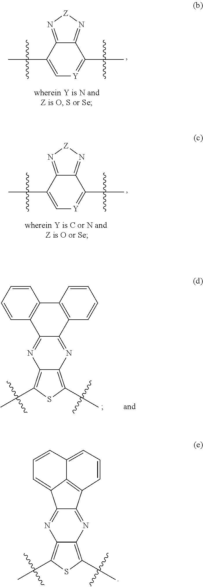
- the polymer semiconductors described herein contain at least one divalent linkage providing compound selected from the group consisting of an aromatic or heteroaromatic electron acceptor compound X and an aromatic or heteroaromatic compound Y.
- the aromatic or heteroaromatic electron acceptor compound X may be a fused aromatic semiconductor compound or a fused aromatic semiconductor compound. Any electron acceptor compound may be used provided the electron acceptor compound stabilizes the quinodal form of the polymer semiconductor and thus narrows the energy gap of the polymer semiconductor.
- aromatic or heteroaromatic electron acceptor compounds representable by structures II-1 to II-8:
- hydrocarbon group encompasses both unsubstituted hydrocarbon groups and substituted hydrocarbon groups.
- the unsubstituted hydrocarbon group may contain, for example, from about 1 to about 50 carbon atoms, from about 2 to about 40 carbon atoms, from about 2 to about 35 carbon atoms or from about 2 to about 24 carbon atoms.
- unsubstituted hydrocarbon groups may include, for example, a straight chain alkyl group, a branched alkyl group, a cycloalkyl group, an aryl group, an alkylaryl group, and an arylalkyl group.
- Example alkyl groups may include, for example, methyl, ethyl, propyl, butyl, pentyl, hexyl, heptyl, octyl, nonyl, decyl, undecyl, dodecyl, tridecyl, tetradecyl, pentadecyl, cyclopentyl, cyclohexyl, cycloheptyl, and isomeric forms thereof.
- alkyl refers to a substituent composed entirely of carbon atoms and hydrogen atoms which is fully saturated and of the formula C n H 2n+1 , wherein n is an integer that determines the structure of the alkyl substituent.
- An alkyl chain may be linear or branched.
- aryl refers to a substituent composed entirely of carbon atoms and hydrogen atoms which is aromatic.
- the substituted hydrocarbon group may contain, for example, from about 1 to about 70 carbon atoms, from about 10 to about 60 carbon atoms and from about 20 to about 50 carbon atoms substituted with, for example, fluorine, bromine, chlorine, iodine, sulfur, amino, nitro, cyano, methoxyl, ethoxyl, propoxy, or combinations thereof.
- Substituted hydrocarbon groups may be, for example, a straight chain alkyl group, a branched alkyl group, a cycloalkyl group, an aryl group, an alkylaryl group, and an arylalkyl group with a heteroatom.
- Example alkyl groups may include, for example, methyl, ethyl, propyl, butyl, pentyl, hexyl, heptyl, octyl, nonyl, decyl, undecyl, dodecyl, tridecyl, tetradecyl, pentadecyl, cyclopentyl, cyclohexyl, cycloheptyl, and isomeric forms thereof.
- the hydrocarbon group may be optionally substituted alkyl and optionally substituted aryl.
- heteroatom includes fluorine, bromine, chlorine, iodine, sulfur, nitrogen, oxygen, or combinations thereof.
- the heteroatom can be a single atom such as, for example, chlorine or fluorine or the single atom contained in a compound such as, for example, the nitrogen atom (N) in an amino compound (NH 2 ) and the sulfur atom (S) in a SO 2 compound.
- R 1 and R 2 are each alkyl groups having from about 8 to about 24 carbon atoms. In other embodiments, R 1 and R 2 are identical to each other. In one specific example, R 1 and R 2 are each —C 12 H 25 .
- the aromatic or heteroaromatic compound Y may be a substituted or unsubstituted thiophene, bithiophene, thienothiophene, phenylene, biphenylene, phenanthrenylene, dihydrophenanthrenylene, fluorene, carbazole, oligoarylene or mixtures thereof.
- the polymer semiconductors described herein can be prepared by the conjugated cross-coupling reaction of an alkylated benzodithiophene core substituted with a boronic acid (or ester) and an electron acceptor compound disubstituted with a halogen. Such reactions are commonly referred to as “Suzuki couplings”. However, the polymer semiconductors can be prepared by the conjugated cross-coupling reaction of an alkylated benzodithiophene core substituted with a halogen with an electron acceptor compounds substituted with a boronic acid (or ester).
- the semiconductors described herein can also be prepared by other aryl-aryl coupling reactions, such as Yamamoto coupling, Stille coupling, or Heck coupling.
- aryl-aryl coupling reactions such as Yamamoto coupling, Stille coupling, or Heck coupling.
- An examples of suitable cross-coupling reactions are described in U.S. Patent Application Pub. No. 2009/0179198, the disclosure of which is incorporated by references herein in its entirety.
- Other cross-coupling reactions are described in Hou et al., Bandgap and Molecular Energy Level Control of Conjugated Polymer Photovoltaic Materials Based on Benzo[ 1,2-b:4,5-b′]dithiophen, M ACROMOLECULES, 2008, 41, 6012-6018 and Usta et al.
- This two-step process simplifies purification and eliminates reactions using hydrogen gas.
- Another advantage is that this process allows the addition of substituents, such as branched alkyl chains or aryl rings, which are otherwise unaccessable (cannot be placed on the 4 and 8 locations) using the embodiment shown in Scheme 1.
- M is MgX or Li
- X is a halogen
- R 1′ is linear alkyl, branched alkyl, aryl, or heteroaryl.
- the starting benzoquinone-dithiophene or benzodithiophene-4,8-dione A is reacted with reagent B to obtain R 1 substituents at the 4 and 8 positions to obtain an intermediate compound (not shown).
- the intermediate compound is then reduced to form the 4,8-disubstituted benzodithiophene C (Formula 2).
- any reducing agent which does not affect the identity of R 1 can be used.
- SnCl 2 in an acidic solution typically via addition of HCl
- the organomagnesium or organolithium reagent M-R 1 has a pKa of at least 35, i.e. the pKa is 35 or higher. In other words, the reagent is very alkaline.
- An exemplary reagent is dodecylmagnesium bromide, which has a pKa of about 50.
- the pKa of benzoquinone-dithiophene is about 35. This large pKa difference generally leads to undesired side acid-base reactions which reduce the yield of the desired BDT. However, careful selection of the reaction process produces BDTs in reasonable yields.
- the prior art process shown in Scheme 1 utilizes an alkynylmagnesium or alkynyllithium reagent with a pKa of about 25, which avoids these competing side reactions.
- any reducing agent which does not affect the identity of R 1 can be used.
- the reduction is performed using a metal chloride in an acidic solution (typically via addition of HCl).
- exemplary metal chlorides include tin chloride, zinc chloride, and iron chloride.
- SnCl 2 in an acidic solution is used.
- the reagent is typically dissolved in a solvent to form a reagent solution.
- the solvent may be a hydrocarbon solvent, an aromatic solvent, diethyl ether, tert-butylmethyl ether, tetrahydrofuran (THF), 1,4-dioxane, or a mixture thereof.
- Exemplary solvents include cyclohexane, xylene, hexane, heptane, and toluene.
- the solvent is an anhydrous ethereal solvent.
- the benzoquinone-dithiophene is added to a solution of the organomagnesium or organolithium reagent in an anhydrous ethereal solvent.
- concentration of the organomagnesium or organolithium reagent may be from about 0.1 M to about 1.0 M.
- the reaction is typically heated to a range of from about 20° C. to about 120° C., including from about 40° C. to about 80° C. The heating typically lasts for a period of from about 1 hour to about 4 hours. In other embodiments, the heating last for at least 1 hours.
- the reaction is cooled to room temperature and the excess organomagnesium or organolithium reagent is quenched with water.
- the reaction is then treated with an acidic solution of tin chloride.
- concentration of the tin chloride solution is from about 1 M to about 3 M dissolved in a 10 vol % hydrochloric acid solution.
- the reaction is typically heated a range of from about 20° C. to about 120° C., including from about 40° C. to about 80° C.
- the reaction can be heated for a period of at least 1 hour, including from about 2 hours to about 24 hours.
- the reaction is cooled to room temperature and the product C is isolated and purified using standard methods known in the art.
- the product can be purified by a combination of column chromatography and recrystallization.
- the column may use, for example, silica gel. In some embodiments, column chromatography and recrystallization are used to achieve a minimum HPLC purity of 94%.
- the organomagnesium/organolithium reagent B is dissolved in a solvent like hexane or an ethereal solvent/ether containing solvent, such as tetrahydrofuran (THF), 1,4-dioxane, or tert-butylmethyl ether (TBME).
- a solvent like hexane or an ethereal solvent/ether containing solvent, such as tetrahydrofuran (THF), 1,4-dioxane, or tert-butylmethyl ether (TBME).
- THF tetrahydrofuran
- 1,4-dioxane 1,4-dioxane
- TBME tert-butylmethyl ether
- the starting benzoquinone-dithiophene A is then added to the solution to begin the reaction.
- the reaction of the benzoquinone-dithiophene and the reagent occurs in an inert atmosphere, for example argon
- the molar ratio of the reagent to the benzoquinone-dithiophene may be from about 2:1 to about 4:1, to ensure complete addition of substituents to the 4 and 8 positions.
- organomagnesium/organolithium reagent can be added to a suspension of the benzoquinone-dithiophene in an ethereal solvent and the reaction can be completed as described previously with yields of around 30%.
- Salt additives which modify the reactivity of organomagnesium reagents, such as LiCl or LiBr, do not affect the yield of the process and can be added to the reagent solution as well. This process has been demonstrated on a 5 gram scale with similar yields and it is expected that larger batch sizes will give consistent and reproducible yields in the 30% range.
- the polymer semiconductors of Formula (1) can be prepared by the conjugated cross-coupling reaction of these semiconductors with substituted boronic acid (or ester or halogen) and halogenated electron acceptor compound or an electron acceptor compound substituted with boronic acid (or ester).
- Suzuki polycondensation may be used to prepare regioregular, block and random copolymers.
- block copolymers or alternating copolymers, in particular AB-type copolymers may be prepared from a first and a second monomer wherein both reactive groups of the first monomer are boron and both reactive groups of the second monomer are halide.
- the synthesis of block copolymers is described in detail for example in WO 2005/014688 A2, which is incorporated by references herein in its entirety.
- Other synthesis of block copolymer are described in J. Sakamoto et al., Suzuki Polycondensation: Polyarylenes á la Carte , M ACROMOL . R APID C OMMUN. 2009, 30, 653-687 and references contained herein.
- the polymer semiconductors described herein may be produced by copolymerizing an alkylated benzodithiophene core substituted with a boron reagent to an electron acceptor compound disubstituted with a halogen. Furthermore, the polymer semiconductors described herein may also be produced by coupling the electron acceptor compound disubstituted with a halogen with an alkylated benzodithiophene core substituted with a boron reagent. The resulting polymer semiconductor from either copolymerization is an alternating copolymer.
- boron reagents include boronic acids, boronic esters, dialkoxyboranes and bis(alkoxy)diborons that contain a —B(OR′)(OR′′) group, wherein R′ and R′′ are a hydrocarbon group as defined above.
- halogen atoms include chlorine, fluorine, and bromine.
- the benzodithiophene (substituted with a halogen atom or boron reagent at the 2 and 6 positions of the benzodithiophene core) is then copolymerized with the electron acceptor compound X and/or an aromatic or heteroaromatic compound Y, in the presence of a catalyst, to obtain a repeating unit.
- catalysts include a Pd(0) complexes or Pd(II) salts.
- Pd(0) complexes are those bearing at least one phosphine ligand such as tetrakis(triphenylphosphine (Pd(PPh 3 ) 4 ), tris(triortho-tolylphosphine) (Pd(o-Tol) 3 P), Tris(dibenzylideneacetone)dipalladium(0)/triortho-tolylphosphine (Pddba/P(o-Tol) 3 ), palladium(II) (di-t-bpfPdCl 2 ), dichloro bis(tri-ortho-tolylphosphine) palladium(II) (Pd)(o-tol) 3 PCl 2 .
- phosphine ligand such as tetrakis(triphenylphosphine (Pd(PPh 3 ) 4 ), tris(triortho-tolylphosphine) (Pd(o-Tol)
- Pd(II) salts examples include [1,1′-bis(diphenylphosphino)ferrocene]-dichloropalladium (PdCl 2 (dppf)); PdCl 2 (PPh 3 ) 2 ; dichloro 1,1-bis(di-tert-butylphosphino) ferrocene and palladium acetate.
- polymer semiconductors are soluble or substantially soluble in common coating solvents and thus form a polymer solution.
- polymer semiconductors possess a solubility of at least about 0.1 percent by weight, and more specifically, from about 0.3 percent to about 10 percent, or to about 50 percent by weight in such solvents as methylene chloride, chloroform, 1,2-dichloroethane, tetrahydrofuran, toluene, xylene, mesitylene, chlorobenzene, dichlorobenzene, and the like.
- the polymer semiconductors of the formulas as illustrated herein provide a stable conductivity of, for example, from about 10 ⁇ 9 S/cm to about 10 ⁇ 4 S/cm, and more specifically, from about 10 ⁇ 8 S/cm to about 10 ⁇ 5 S/cm as determined by conventional four-probe conductivity measurements.
- Fabrication of a printed organic electronic (POE) device using the polymer solution can be carried out by depositing the polymer solution on a substrate using any suitable liquid deposition technique at any suitable time prior to or subsequent to the formation of other optional layer or layers on the substrate.
- liquid deposition of the polymer solution on the substrate can occur either on a substrate or on a substrate already containing layered material, for example, a semiconductor layer and/or an insulating layer of a thin-film transistor.
- liquid deposition technique refers to, for example, deposition of a composition using a liquid process such as liquid coating or printing technique, where the liquid is a homogeneous or heterogeneous dispersion of the polymer semiconductors in a solvent.
- the polymer solution may be deposited in any suitable pattern on the substrate.
- liquid coating processes may include, for example, spin coating, blade coating, rod coating, dip coating, and the like.
- printing techniques may include, for example, lithography or offset printing, gravure, flexography, screen printing, stencil printing, inkjet printing, stamping (such as microcontact printing), and the like.
- liquid deposition of the polymer solution deposits a layer of the polymer semiconductor having a thickness ranging from about 5 nanometers to about 5 millimeters, from about 10 nanometers to about 1000 micrometers, from about 100 nanometers to about 500 micrometers, from about 1 micrometer to about 100 micrometers and from about 5 micrometers to about 25 micrometers.
- the deposited polymer solution at this stage may or may not exhibit appreciable electrical conductivity.
- Heating the polymer solution a temperature of, for example, at or below about 150° C. or at or below about 130° C., such as, for example, from about 50° C. to about 150° C., from about 50° C. to about 130° C., from about 50° C. to about 80° C., from about 100° C. to about 130° C. and from about 100° C. to about 120° C., to remove the solvent from the polymer solution and thus form a layer comprising the polymer semiconductors of Formula (1) on the substrate.
- the heating temperature is one that does not cause adverse changes in the properties of previously deposited layer(s) or the substrate (whether single layer substrate or multilayer substrate).
- the heating can be performed for a time ranging from, for example, 1 second to about 10 hours and from about 10 seconds to 1 hour.
- the heating can be performed in air, in an inert atmosphere, for example, under nitrogen or argon, or in a reducing atmosphere, for example, under nitrogen containing from 1 to about 20 percent by volume hydrogen.
- the heating can also be performed under normal atmospheric pressure or at a reduced pressure of, for example, from about 1000 mbars to about 0.01 mbars.
- heating encompasses any technique(s) that can impart sufficient energy to remove the solvent from the substrate.
- heating techniques may include thermal heating (for example, a hot plate, an oven, and a burner), infra-red (“IR”) radiation, a laser beam, microwave radiation, or UV radiation, or a combination thereof.
- the polymer semiconductor of Formula (1) may be used in electronic devices such as thin-film transistors, diodes and photovoltaic devices, such as polymer solar cells (PSCs).
- PSCs polymer solar cells
- the use of the present polymer as a semiconductor in electronic devices is illustrated herein using thin-film transistors and photovoltaic devices.
- a thin-film transistor comprising:
- gate dielectric layer, the gate electrode, the semiconductor layer, the source electrode, the drain electrode and the substrate layer are in any sequence as long as the gate electrode and the semiconductor layer both contact the gate dielectric layer, and the source electrode and the drain electrode both contact the semiconductor layer, and the semiconductor layer is comprised of the polymer semiconductor compounds described herein.
- the substrate layer may generally be a silicon material inclusive of various appropriate forms of silicon, a glass plate, a plastic film or a sheet, and the like depending on the intended applications.
- a plastic substrate such as for example polyester, polycarbonate, polyimide sheets, and the like, may be selected.
- the thickness of the substrate may be, for example, from about 10 micrometers to about 100 millimeters with a specific thickness being from about 50 to about 100 micrometers, especially for a flexible plastic substrate, and from about 1 to about 10 millimeters for a rigid substrate such as glass or silicon.
- the gate dielectric layer which can separate the gate electrode from the source and drain electrodes, and in contact with the semiconductor layer, can generally be an inorganic material film, an organic polymer film, or an organic-inorganic composite film.
- the thickness of the gate dielectric layer can be, for example, from about 10 nanometers to about 1 micrometer with a more specific thickness being about 100 nanometers to about 500 nanometers.
- inorganic materials suitable as the dielectric layer may include silicon oxide, silicon nitride, aluminum oxide, barium titanate, barium zirconate titanate and the like.
- Examples of organic polymers for the dielectric layer may include polyesters, polycarbonates, poly(vinyl phenol), polyimides, polystyrene, poly(methacrylate)s, poly(acrylate)s, epoxy resin and the like.
- Examples of inorganic-organic composite materials may include nanosized metal oxide particles dispersed in polymers, such as polyester, polyimide, epoxy resin and the like.
- the gate dielectric layer is generally of a thickness of from about 50 nanometers to about 500 nanometers depending on the dielectric constant of the dielectric material used.
- the dielectric material has a dielectric constant of, for example, at least about 3, thus a suitable dielectric thickness of about 300 nanometers can provide a desirable capacitance, for example, of about 10 ⁇ 9 to about 10 ⁇ 7 F/cm 2 .
- the active semiconductor layer comprised of polymer semiconductors of the Formulas as illustrated herein, and wherein the thickness of this layer is generally, for example, about 10 nanometers to about 1 micrometer, or about 40 to about 100 nanometers.
- This layer can generally be fabricated by solution processes such as spin coating, casting, screen, stamp, or jet printing of a solution of polymer semiconductors of the present disclosure.
- the gate electrode can be a thin metal film, a conducting polymer film, a conducting film generated from a conducting ink or paste, or the substrate itself (for example heavily doped silicon).
- the gate electrode materials may include gold, silver, chromium, indium tin oxide, conducting polymers, such as polystyrene sulfonate-doped poly(3,4-ethylenedioxythiophene) (PSS/PEDOT), a conducting ink/paste comprised of carbon black/graphite or colloidal silver dispersion contained in a polymer binder, such as Electrodag available from Acheson Colloids Company, and silver filled electrically conductive thermoplastic ink available from Noelle Industries, and the like.
- the gate layer may be prepared by vacuum evaporation, sputtering of metals or conductive metal oxides, coating from conducting polymer solutions or conducting inks, or dispersions by spin coating, casting or printing.
- the thickness of the gate electrode layer may be, for example, from about 10 nanometers to about 10 micrometers, and a specific thickness may be, for example, from about 10 to about 200 nanometers for metal films, and about 1 to about 10 micrometers for polymer conductors.
- the source and drain electrode layer can be fabricated from materials which provide a low resistance ohmic contact to the semiconductor layer.
- Typical materials suitable for use as source and drain electrodes may include those of the gate electrode materials such as gold, nickel, aluminum, platinum, conducting polymers, and conducting inks.
- Typical thickness of this layer may be, for example, from about 40 nanometers to about 1 micrometer with the more specific thickness being about 100 to about 400 nanometers.
- the TFT devices contain a semiconductor channel with a width W and length L.
- the semiconductor channel width may be, for example, from about 10 micrometers to about 5 millimeters with a specific channel width being about 100 micrometers to about 1 millimeter.
- the semiconductor channel length may be, for example, from about 1 micrometer to about 1 millimeter with a more specific channel length being from about 5 micrometers to about 100 micrometers.
- the source electrode is grounded and a bias voltage of generally, for example, about 0 volts to about ⁇ 80 volts is applied to the drain electrode to collect the charge carriers transported across the semiconductor channel when a voltage of generally, for example, about +10 volts to about ⁇ 80 volts is applied to the gate electrode.
- the annealing temperature for a thin-film transistor comprised of a polymer semiconductor layer having the polymer semiconductor compounds according to the Formulas herein is about or below about 150° C., about or below about 125° C. or about or below about 100° C.
- FIG. 1 illustrates a TFT configuration comprised of a substrate ( 16 ) in contact with a gate electrode ( 18 ) and with a gate dielectric layer ( 14 ) containing the gate electrode ( 18 ).
- the gate dielectric layer ( 14 ) On top of the gate dielectric layer ( 14 ) are the source electrode ( 20 ) and the drain electrode ( 22 ).
- the polymer semiconductor layer ( 12 ) Above and situated between the source electrode ( 20 ) and the drain electrode ( 22 ) is the polymer semiconductor layer ( 12 ),
- the gate electrode ( 18 ) can be included in the substrate ( 16 ), in the gate dielectric layer ( 14 ), and the like throughout.
- FIG. 2 illustrates a TFT configuration comprised of a substrate ( 16 ) in contact with a gate electrode ( 18 ) and with a gate dielectric layer ( 14 ) containing the gate electrode ( 18 ).
- a gate dielectric layer ( 14 ) On top of the gate dielectric layer ( 14 ) is the polymer semiconductor layer ( 12 ).
- the source electrode ( 20 ) and the drain electrode ( 22 ) Above the polymer semiconductor layer ( 12 ) are the source electrode ( 20 ) and the drain electrode ( 22 ).
- the polymer semiconductors described herein may also be used in photovoltaic devices, such as polymer solar cells (PSCs).
- PSCs polymer solar cells
- the inclusion of the polymer semiconductors described may lead to a photovoltaic device with a lower manufacturing cost, possess a low band gap polymer for broad light absorption that leads to increased efficiency in the photovoltaic device and is lightweight and has increased flexibility when compared to silicon solar cells.
- a photovoltaic device comprising:
- the substrate, the first electrode, the second electrode and the thin-film layer are in any sequence as long as the first electrode and the second electrode both contact the thin-film layer, and the thin-film layer is comprised of the polymer semiconductor compounds described herein.
- the substrate layer may generally be a silicon material inclusive of various appropriate forms of silicon, a glass plate, a plastic film or a sheet, and the like depending on the intended applications.
- a plastic substrate such as for example polyester, polycarbonate, polyimide sheets, and the like, may be selected.
- the thickness of the substrate may be, for example, from about 10 micrometers to about 100 millimeters with a specific thickness being from about 50 to about 100 micrometers, especially for a flexible plastic substrate, and from about 1 to about 10 millimeters for a rigid substrate such as glass or silicon.
- the thin-film layer comprised of polymer semiconductors of the formulas as illustrated herein, and wherein the thickness of this layer is generally, for example, about 10 nanometers to about 1 micrometer, or about 40 to about 100 nanometers.
- This layer can generally be fabricated by solution processes such as spin coating, casting, screen, stamp, or jet printing of a solution of polymer semiconductors of the present disclosure.
- the first and second electrode can be a thin metal film, a conducting polymer film, a conducting film generated from a conducting ink or paste, or the substrate itself (for example heavily doped silicon).
- the first and second electrode materials may include silver, gold, chromium, fluorine-doped tin oxide (“FTO”), ZnO—Ga 2 O 3 , ZnO—Al 2 O 3 , and SnO 2 —Sb 2 O 3 .
- first electrode and/or second electrode layer be prepared by vacuum evaporation, sputtering of metals or conductive metal oxides, coating from conducting polymer solutions or conducting inks, or dispersions by spin coating, casting or printing.
- the thickness of the first and/or second electrode layer may be, for example, from about 10 nanometers to about 10 micrometers, and a specific thickness may be, for example, from about 10 to about 200 nanometers for metal films, and about 1 to about 10 micrometers for polymer conductors.
- FIG. 3 illustrates a photovoltaic cell configuration comprised of a substrate ( 30 ) in contact with a first electrode ( 32 ).
- a first electrode 32
- the thin-film layer 34
- the second electrode 36
- the reaction was treated with a solution of tin(II) chloride (12.91 grams, 68.1 mmol) in 10 vol % hydrochloric acid solution (30 mL) and was heated to 60° C. After 18 hours, the heating bath was removed and the reaction was cooled to room temperature. The layers were separated and the organic layer was dried (using MgSO 4 ), filtered and concentrated using a rotary evaporator.
- the crude product was passed through a short SiO 2 plug using hexanes as eluent, and the product was recrystallized from hexanes yielding 4,8-didodecylbenzo[1,2-b:4,5-b′]dithiophene as a white solid (1.7 grams, 28% yield). The structure was confirmed by 1 H and 13 C NMR spectroscopy.
- Example 3 is based upon Scheme 4 illustrated below and the Suzuki polymerization reaction described in M. Zhang et al., Field - Effect Transistors Based on a Benzothiadiazole - Cyclopentadithiophene Copolymer, J. Am. Chem. Soc. 2007, 129, 3472-3473.
Abstract

and at least one divalent linkage providing compound selected from the group consisting of an aromatic or heteroaromatic electron acceptor compound X and an aromatic or heteroaromatic compound Y, wherein R1 and R2 are side chains independently selected from the group consisting of a hydrogen atom, a hydrocarbon group, a heteroatom and combinations thereof.
Description

and at least one divalent linkage providing compound selected from the group consisting of an aromatic or heteroaromatic electron acceptor compound X, an aromatic or heteroaromatic compound Y and combinations thereof, wherein R1 and R2 are side chains independently selected from the group consisting of a hydrogen atom, a hydrocarbon group, a heteroatom and combinations thereof.

substituting the 2 and 6 positions of the benzodithiophene with at least one boron reagent or at least one halogen atom, copolymerizing at least one divalent linkage providing compound selected from the group consisting of an aromatic or heteroaromatic electron acceptor compound X and an aromatic or heteroaromatic compound Y to the 2 and 6 positions of the benzodithiophene to obtain a repeating unit; and polymerizing the repeating unit to obtain the polymer semiconductor.

and at least one divalent linkage providing compound selected from the group consisting of an aromatic or heteroaromatic electron acceptor compound X and an aromatic or heteroaromatic compound Y, wherein R1 and R2 are side chains independently selected from the group consisting of a hydrogen atom, a hydrocarbon group, a heteroatom and combinations thereof.


and at least one divalent linkage providing compound selected from the group consisting of an aromatic or heteroaromatic electron acceptor compound X and an aromatic or heteroaromatic compound Y, wherein R1 and R2 are side chains independently selected from the group consisting of a hydrogen atom, a hydrocarbon group, a heteroatom and combinations thereof.

wherein R1 and R2 are side chains independently selected from the group consisting of a hydrogen atom, a hydrocarbon group, a heteroatom and combinations thereof, X is an aromatic or heteroaromatic electron acceptor compound, and n is the number of repeating units of from about 2 to about 5000, of from about 2 to about 3000 or from about 5 to about 1000, from about 5 to about 800, from about 5 to about 200 or from about 5 to about 75.


wherein M is MgX or Li, X is a halogen, and R1′ is linear alkyl, branched alkyl, aryl, or heteroaryl. The starting benzoquinone-dithiophene or benzodithiophene-4,8-dione A is reacted with reagent B to obtain R1 substituents at the 4 and 8 positions to obtain an intermediate compound (not shown). The intermediate compound is then reduced to form the 4,8-disubstituted benzodithiophene C (Formula 2). In the reduction step, generally any reducing agent which does not affect the identity of R1 can be used. However, in particular embodiments, SnCl2 in an acidic solution (typically via addition of HCl) is used.

Claims (13)


Priority Applications (8)
| Application Number | Priority Date | Filing Date | Title |
|---|---|---|---|
| US12/689,613 US8304512B2 (en) | 2010-01-19 | 2010-01-19 | Benzodithiophene based materials compositions |
| DE102011002579A DE102011002579A1 (en) | 2010-01-19 | 2011-01-12 | Benzodithiophene-based material compositions |
| CA2727497A CA2727497A1 (en) | 2010-01-19 | 2011-01-12 | Benzodithiophene based materials compositions |
| TW100101208A TW201134849A (en) | 2010-01-19 | 2011-01-13 | Benzodithiophene based materials compositions |
| GB1100733.3A GB2477194B (en) | 2010-01-19 | 2011-01-17 | Benzodithiophene based materials compositions |
| JP2011006629A JP2011151396A (en) | 2010-01-19 | 2011-01-17 | Polymer semiconductor, method of manufacturing polymer semiconductor and electronic device |
| CN2011100226269A CN102127210A (en) | 2010-01-19 | 2011-01-18 | Benzodithiophene based materials compositions |
| KR1020110005062A KR101831859B1 (en) | 2010-01-19 | 2011-01-18 | Polymer semiconductor and method of manufacturing the same and electronic device |
Applications Claiming Priority (1)
| Application Number | Priority Date | Filing Date | Title |
|---|---|---|---|
| US12/689,613 US8304512B2 (en) | 2010-01-19 | 2010-01-19 | Benzodithiophene based materials compositions |
Publications (2)
| Publication Number | Publication Date |
|---|---|
| US20110178255A1 US20110178255A1 (en) | 2011-07-21 |
| US8304512B2 true US8304512B2 (en) | 2012-11-06 |
Family
ID=43736527
Family Applications (1)
| Application Number | Title | Priority Date | Filing Date |
|---|---|---|---|
| US12/689,613 Active US8304512B2 (en) | 2010-01-19 | 2010-01-19 | Benzodithiophene based materials compositions |
Country Status (8)
| Country | Link |
|---|---|
| US (1) | US8304512B2 (en) |
| JP (1) | JP2011151396A (en) |
| KR (1) | KR101831859B1 (en) |
| CN (1) | CN102127210A (en) |
| CA (1) | CA2727497A1 (en) |
| DE (1) | DE102011002579A1 (en) |
| GB (1) | GB2477194B (en) |
| TW (1) | TW201134849A (en) |
Cited By (4)
| Publication number | Priority date | Publication date | Assignee | Title |
|---|---|---|---|---|
| US20140124035A1 (en) * | 2010-01-05 | 2014-05-08 | Merck Patent Gmbh | Photovoltaic cell with benzodithiophene-containing polymer |
| US9559305B2 (en) | 2012-03-16 | 2017-01-31 | Merck Patent Gmbh | Conjugated polymers |
| US9577197B2 (en) | 2011-07-21 | 2017-02-21 | Merck Patent Gmbh | Conjugated polymers |
| US10050201B2 (en) | 2010-04-19 | 2018-08-14 | Merck Patent Gmbh | Polymers of benzodithiophene and their use as organic semiconductors |
Families Citing this family (16)
| Publication number | Priority date | Publication date | Assignee | Title |
|---|---|---|---|---|
| US9365585B2 (en) * | 2010-02-15 | 2016-06-14 | Merck Patent Gmbh | Semiconducting polymers |
| CN102637636A (en) * | 2011-08-24 | 2012-08-15 | 京东方科技集团股份有限公司 | Organic thin-film transistor array substrate, method for manufacturing same and display device |
| ITMI20112405A1 (en) | 2011-12-28 | 2013-06-29 | Eni Spa | PHOTOLUMINESCENT COMPOUND OR MIXTURE OF PHOTOLUMINESCENT COMPOUNDS |
| JP6069787B2 (en) * | 2012-03-08 | 2017-02-01 | 学校法人早稲田大学 | Benzodithiophenequinone polymer, charge storage material, electrode active material, electrode, and battery |
| KR101424978B1 (en) * | 2012-05-24 | 2014-07-31 | 경상대학교산학협력단 | Novel method for preparing hetero fused ring compounds using gilman reagent compounds |
| JP6207606B2 (en) * | 2012-07-23 | 2017-10-04 | ビーエーエスエフ ソシエタス・ヨーロピアBasf Se | Dithienobenzofuran polymers and small molecules for electronic applications |
| CN103664994A (en) * | 2012-08-31 | 2014-03-26 | 昆山维信诺显示技术有限公司 | Benzodithiophene derivative organic electroluminescent material and application thereof |
| CN104640902B (en) * | 2012-09-14 | 2017-09-01 | 东丽株式会社 | It is conjugated based polymer, the electron donating property organic material for having used the conjugation based polymer, photovoltaic element material and photovoltaic element |
| EP2927260B1 (en) * | 2012-11-30 | 2017-05-03 | Ocean's King Lighting Science & Technology Co., Ltd. | Benzodithiophene based copolymer containing isoindoline-1,3-diketone units and preparing method and applications thereof |
| CN104045818B (en) * | 2013-03-13 | 2016-08-24 | 海洋王照明科技股份有限公司 | A kind of containing allene contracting thiourea-carbazole-benzo two thiophene copolymers and preparation method and application |
| JP6103585B2 (en) * | 2013-03-27 | 2017-03-29 | オリヱント化学工業株式会社 | Method for producing thienothiophene-benzodithiophene copolymer |
| CN103467712B (en) * | 2013-08-27 | 2015-10-14 | 上海交通大学 | The semi-conducting polymer of two dimension conjugation naphtho-difuryl and preparation thereof, purposes |
| JP6280208B2 (en) | 2014-03-24 | 2018-02-14 | 株式会社東芝 | Polymer and solar cell using the same |
| CN104119354B (en) * | 2014-05-14 | 2016-08-24 | 杭州师范大学 | A kind of cross benzo two thiophene compound and preparation method thereof |
| JP5957564B1 (en) | 2015-03-23 | 2016-07-27 | 株式会社東芝 | Polymer and solar cell using the same |
| KR102103060B1 (en) * | 2017-05-24 | 2020-04-21 | 주식회사 엘지화학 | Compound and organic solar cell comprising the same |
Citations (33)
| Publication number | Priority date | Publication date | Assignee | Title |
|---|---|---|---|---|
| WO2005014688A2 (en) | 2003-08-12 | 2005-02-17 | Covion Organic Semiconductors Gmbh | Conjugated copolymers, representation and use thereof |
| US20050082525A1 (en) * | 2003-10-15 | 2005-04-21 | Martin Heeney | Poly(benzodithiophenes) |
| US20050277776A1 (en) * | 2004-06-10 | 2005-12-15 | Xerox Corporation | Processes to prepare small molecular thiophene compounds |
| US20070112171A1 (en) | 2005-11-16 | 2007-05-17 | Xerox Corporation | Polymer having thieno[3,2-b] thiophene moieties statement regarding federally sponsored research or development |
| US20070145453A1 (en) | 2005-12-23 | 2007-06-28 | Xerox Corporation | Dielectric layer for electronic devices |
| US20070148812A1 (en) | 2005-12-22 | 2007-06-28 | Xerox Corporation | Organic thin-film transistors |
| US20070145357A1 (en) | 2005-12-23 | 2007-06-28 | Xerox Corporation | Thin-film transistor |
| US20070145371A1 (en) | 2005-12-23 | 2007-06-28 | Xerox Corporation | Thin-film transistor |
| US7256418B2 (en) | 2002-01-11 | 2007-08-14 | Xerox Corporation | Polythiophenes and devices thereof |
| JP2007246579A (en) | 2006-03-14 | 2007-09-27 | Ricoh Co Ltd | New benzodithiophene polymer |
| US20070235719A1 (en) | 2006-04-06 | 2007-10-11 | Xerox Corporation | Poly(alkynylthiophene)s and electronic devices generated therefrom |
| US20070235726A1 (en) | 2006-04-06 | 2007-10-11 | Xerox Corporation | Poly[bis(ethynyl)heteroacene]s and electronic devices generated therefrom |
| US20070284572A1 (en) | 2002-01-11 | 2007-12-13 | Xerox Corporation | Polythiophenes and devices thereof |
| US20080006324A1 (en) * | 2005-07-14 | 2008-01-10 | Konarka Technologies, Inc. | Tandem Photovoltaic Cells |
| US20080102559A1 (en) | 2006-10-25 | 2008-05-01 | Xerox Corporation | Electronic devices |
| US20080103286A1 (en) | 2006-10-25 | 2008-05-01 | Xerox Corporation | Poly(dithienylbenzo[1,2-B:4,5-B']dithiophene) polymers |
| US20080103314A1 (en) | 2005-11-16 | 2008-05-01 | Xerox Corporation | Small molecule compound having indolocarbazole moiety and divalent linkage |
| US20080108834A1 (en) | 2004-06-10 | 2008-05-08 | Xerox Corporation | Small molecular thiophene compound having divalent linkage |
| US20080108833A1 (en) | 2004-06-10 | 2008-05-08 | Xerox Corporation | Small molecular thiophene compound |
| US20080146776A1 (en) | 2006-12-14 | 2008-06-19 | Xerox Corporation | Thiophene electronic devices |
| US20090114909A1 (en) | 2005-11-16 | 2009-05-07 | Xerox Corporation | Device containing polymer having indolocarbazole- repeat unit and divalent linkage |
| US20090140237A1 (en) | 2007-11-29 | 2009-06-04 | Xerox Corporation | Thin film transistors |
| US20090140236A1 (en) | 2007-11-29 | 2009-06-04 | Xerox Corporation | Thin film transistors |
| US20090181509A1 (en) | 2008-01-14 | 2009-07-16 | Xerox Corporation | Polymer semiconductors with high mobility |
| US20090179194A1 (en) | 2008-01-16 | 2009-07-16 | Xerox Corporation | Organic thin film transistors |
| US20090179198A1 (en) | 2006-07-17 | 2009-07-16 | E.I. Du Pont De Nemours And Company | Thin film transistor comprising novel conductor and dielectric compositions |
| US20090217980A1 (en) | 2005-03-04 | 2009-09-03 | Heliatek Gmbh | Organic Photoactive Device |
| US20090256138A1 (en) | 2008-04-11 | 2009-10-15 | Xerox Corporation | Organic thin film transistor |
| US20090256139A1 (en) | 2008-04-11 | 2009-10-15 | Xerox Corporation | Thin-film transistors |
| WO2010036494A1 (en) | 2008-09-29 | 2010-04-01 | The Regents Of The Univeristy Of California | Active materials for photoelectric devices |
| WO2010135701A1 (en) | 2009-05-21 | 2010-11-25 | Polyera Corporation | Conjugated polymers and their use in optoelectronic devices |
| US20110040069A1 (en) | 2008-02-13 | 2011-02-17 | Osaka University | Condensed polycyclic compound, condensed polycyclic polymer and organic thin film containing the compound or the polymer |
| EP2307483A1 (en) | 2008-07-18 | 2011-04-13 | University Of Chicago | Semiconducting polymers |
-
2010
- 2010-01-19 US US12/689,613 patent/US8304512B2/en active Active
-
2011
- 2011-01-12 DE DE102011002579A patent/DE102011002579A1/en active Pending
- 2011-01-12 CA CA2727497A patent/CA2727497A1/en not_active Abandoned
- 2011-01-13 TW TW100101208A patent/TW201134849A/en unknown
- 2011-01-17 GB GB1100733.3A patent/GB2477194B/en active Active
- 2011-01-17 JP JP2011006629A patent/JP2011151396A/en active Pending
- 2011-01-18 CN CN2011100226269A patent/CN102127210A/en active Pending
- 2011-01-18 KR KR1020110005062A patent/KR101831859B1/en active IP Right Grant
Patent Citations (35)
| Publication number | Priority date | Publication date | Assignee | Title |
|---|---|---|---|---|
| US20070284572A1 (en) | 2002-01-11 | 2007-12-13 | Xerox Corporation | Polythiophenes and devices thereof |
| US7256418B2 (en) | 2002-01-11 | 2007-08-14 | Xerox Corporation | Polythiophenes and devices thereof |
| WO2005014688A2 (en) | 2003-08-12 | 2005-02-17 | Covion Organic Semiconductors Gmbh | Conjugated copolymers, representation and use thereof |
| US20050082525A1 (en) * | 2003-10-15 | 2005-04-21 | Martin Heeney | Poly(benzodithiophenes) |
| US20050277776A1 (en) * | 2004-06-10 | 2005-12-15 | Xerox Corporation | Processes to prepare small molecular thiophene compounds |
| US20080108833A1 (en) | 2004-06-10 | 2008-05-08 | Xerox Corporation | Small molecular thiophene compound |
| US20080108834A1 (en) | 2004-06-10 | 2008-05-08 | Xerox Corporation | Small molecular thiophene compound having divalent linkage |
| US20090217980A1 (en) | 2005-03-04 | 2009-09-03 | Heliatek Gmbh | Organic Photoactive Device |
| US20080006324A1 (en) * | 2005-07-14 | 2008-01-10 | Konarka Technologies, Inc. | Tandem Photovoltaic Cells |
| US20080103314A1 (en) | 2005-11-16 | 2008-05-01 | Xerox Corporation | Small molecule compound having indolocarbazole moiety and divalent linkage |
| US20070112171A1 (en) | 2005-11-16 | 2007-05-17 | Xerox Corporation | Polymer having thieno[3,2-b] thiophene moieties statement regarding federally sponsored research or development |
| US20090124788A1 (en) | 2005-11-16 | 2009-05-14 | Xerox Corporation | POLYMER HAVING THIENO[3,2-b] THIOPHENE MOIETIES |
| US20090114909A1 (en) | 2005-11-16 | 2009-05-07 | Xerox Corporation | Device containing polymer having indolocarbazole- repeat unit and divalent linkage |
| US20070148812A1 (en) | 2005-12-22 | 2007-06-28 | Xerox Corporation | Organic thin-film transistors |
| US20070145357A1 (en) | 2005-12-23 | 2007-06-28 | Xerox Corporation | Thin-film transistor |
| US20070145453A1 (en) | 2005-12-23 | 2007-06-28 | Xerox Corporation | Dielectric layer for electronic devices |
| US20070145371A1 (en) | 2005-12-23 | 2007-06-28 | Xerox Corporation | Thin-film transistor |
| JP2007246579A (en) | 2006-03-14 | 2007-09-27 | Ricoh Co Ltd | New benzodithiophene polymer |
| US20070235719A1 (en) | 2006-04-06 | 2007-10-11 | Xerox Corporation | Poly(alkynylthiophene)s and electronic devices generated therefrom |
| US20070235726A1 (en) | 2006-04-06 | 2007-10-11 | Xerox Corporation | Poly[bis(ethynyl)heteroacene]s and electronic devices generated therefrom |
| US20090179198A1 (en) | 2006-07-17 | 2009-07-16 | E.I. Du Pont De Nemours And Company | Thin film transistor comprising novel conductor and dielectric compositions |
| US20080103286A1 (en) | 2006-10-25 | 2008-05-01 | Xerox Corporation | Poly(dithienylbenzo[1,2-B:4,5-B']dithiophene) polymers |
| US20080102559A1 (en) | 2006-10-25 | 2008-05-01 | Xerox Corporation | Electronic devices |
| US20080146776A1 (en) | 2006-12-14 | 2008-06-19 | Xerox Corporation | Thiophene electronic devices |
| US20090140237A1 (en) | 2007-11-29 | 2009-06-04 | Xerox Corporation | Thin film transistors |
| US20090140236A1 (en) | 2007-11-29 | 2009-06-04 | Xerox Corporation | Thin film transistors |
| US20090181509A1 (en) | 2008-01-14 | 2009-07-16 | Xerox Corporation | Polymer semiconductors with high mobility |
| US20090179194A1 (en) | 2008-01-16 | 2009-07-16 | Xerox Corporation | Organic thin film transistors |
| US20110040069A1 (en) | 2008-02-13 | 2011-02-17 | Osaka University | Condensed polycyclic compound, condensed polycyclic polymer and organic thin film containing the compound or the polymer |
| US20090256138A1 (en) | 2008-04-11 | 2009-10-15 | Xerox Corporation | Organic thin film transistor |
| US20090256139A1 (en) | 2008-04-11 | 2009-10-15 | Xerox Corporation | Thin-film transistors |
| EP2307483A1 (en) | 2008-07-18 | 2011-04-13 | University Of Chicago | Semiconducting polymers |
| WO2010036494A1 (en) | 2008-09-29 | 2010-04-01 | The Regents Of The Univeristy Of California | Active materials for photoelectric devices |
| US20100078074A1 (en) * | 2008-09-29 | 2010-04-01 | The Regents Of The University Of California | Active materials for photoelectric devices and devices that use the materials |
| WO2010135701A1 (en) | 2009-05-21 | 2010-11-25 | Polyera Corporation | Conjugated polymers and their use in optoelectronic devices |
Non-Patent Citations (19)
| Title |
|---|
| C. Du et al., Fused-seven ring Anthracene Derivative With two Sulfur Bridges for High Performance Red Organic light-emitting Diodes, The Royal Society of Chemistry, 2010, 3 pgs. |
| Chao-Ying Yu et al., Thiophene/Phenylene/Thiophene-Based Low-Bandgap Conjugated Polymers for Efficient Near-Infrared Photovoltaic Applications, Chem. Materials, vol. 21, No. 14, 2009, pp. 3262-3269. |
| Foreign search report dated Mar. 20, 2012 issued in German Patent Application No. 10 2011 002 579.0. |
| Great Britain Search Report in Great Britain Application No. GB 1100733.3, dated May 17, 2011. |
| H. Usta et al. Air-Stable, Solution-Processable n-Channel and Ambipolar Semiconductors for Thin-Film Transistors Based on the Indenofluorenebis(dicyanovinylene) Core, J. Am. Chem. Soc. 2008, 130 (27), 8580-8581. |
| J. Hou et al., Bandgap and Molecular Energy Level Control of Conjugated Polymer Photovoltaic Materials Based on Benzo[1,2-b:4,5-b']dithiophen, Macromolecules, 2008, 41, 6012-6018. |
| J. Hou et al., Bandgap and Molecular Energy Level Control of Conjugated Polymer Photovoltaic Materials Based on Benzo[1,2-b:4,5-b′]dithiophen, Macromolecules, 2008, 41, 6012-6018. |
| J. Sakamoto et al., Suzuki Polycondensation: Polyarylenes à la Carte, Macromol. Rapid Commun. 2009, 30, 653-687. |
| L. Huo et al., "A Polybenzo[1,2-b:4,5-b']dithiophene Derivative with Deep HOMO Level and Its Application in High-Performance Polymer Solar Cells", Angewandte Chemie Int. Ed., vol. 49, p. 1-5, (2010), Jan. 25, 2010 published online. |
| L. Huo et al., "A Polybenzo[1,2-b:4,5-b′]dithiophene Derivative with Deep HOMO Level and Its Application in High-Performance Polymer Solar Cells", Angewandte Chemie Int. Ed., vol. 49, p. 1-5, (2010), Jan. 25, 2010 published online. |
| M. Zhang et al., Field-Effect Transistors Based on a Benzothiadiazole-Cyclopentadithiophene Copolymer, J. Am.. Chem. Soc., 2007, 129, 3472-3473. |
| M. Zhang et al., Field-Effect Transistors Based on a Benzothiadiazole—Cyclopentadithiophene Copolymer, J. Am.. Chem. Soc., 2007, 129, 3472-3473. |
| Office Action dated Jul. 5, 2012 issued in Canadian Patent Application No. 2,727,497. |
| Pan et al. (JACS, 2007, 129, 4112-4113). * |
| T. Terao et al., Palladium-Catalyzed Cross-Coupling of Benzyl Ketones and alpha,beta-Unsaturated Carbonyl and Phenolic Compounds with o-Dibromobenzenes to Produce Cyclic Products, Bull. Chem. Soc. JPN., vol. 72, 1999, pp. 2345-2350. |
| T. Terao et al., Palladium-Catalyzed Cross-Coupling of Benzyl Ketones and α,β-Unsaturated Carbonyl and Phenolic Compounds with o-Dibromobenzenes to Produce Cyclic Products, Bull. Chem. Soc. JPN., vol. 72, 1999, pp. 2345-2350. |
| U.S. Appl. No. 12/575,701, filed Oct. 8, 2009. |
| U.S. Appl. No. 13/043,206, filed Mar. 8, 2011. |
| Y. Liang et al., Development of New Semiconducting Polymers for High Performance Solar Cells, J. Am. Chem. Soc. 2009, 131, 56-57. |
Cited By (6)
| Publication number | Priority date | Publication date | Assignee | Title |
|---|---|---|---|---|
| US20140124035A1 (en) * | 2010-01-05 | 2014-05-08 | Merck Patent Gmbh | Photovoltaic cell with benzodithiophene-containing polymer |
| US9337358B2 (en) * | 2010-01-05 | 2016-05-10 | Merck Patent Gmbh | Photovoltaic cell with benzodithiophene-containing polymer |
| US10050201B2 (en) | 2010-04-19 | 2018-08-14 | Merck Patent Gmbh | Polymers of benzodithiophene and their use as organic semiconductors |
| US10158079B2 (en) | 2010-04-19 | 2018-12-18 | Merck Patent Gmbh | Polymers of benzodithiophene and their use as organic semiconductors |
| US9577197B2 (en) | 2011-07-21 | 2017-02-21 | Merck Patent Gmbh | Conjugated polymers |
| US9559305B2 (en) | 2012-03-16 | 2017-01-31 | Merck Patent Gmbh | Conjugated polymers |
Also Published As
| Publication number | Publication date |
|---|---|
| GB201100733D0 (en) | 2011-03-02 |
| JP2011151396A (en) | 2011-08-04 |
| CA2727497A1 (en) | 2011-07-19 |
| CN102127210A (en) | 2011-07-20 |
| TW201134849A (en) | 2011-10-16 |
| KR20110085911A (en) | 2011-07-27 |
| KR101831859B1 (en) | 2018-02-23 |
| US20110178255A1 (en) | 2011-07-21 |
| DE102011002579A1 (en) | 2011-07-21 |
| GB2477194B (en) | 2016-05-04 |
| GB2477194A (en) | 2011-07-27 |
Similar Documents
| Publication | Publication Date | Title |
|---|---|---|
| US8304512B2 (en) | Benzodithiophene based materials compositions | |
| US7932344B2 (en) | Diketopyrrolopyrrole-based polymers | |
| US7820782B2 (en) | Poly(dithienylbenzo[1,2-b:4,5-b′]dithiophene) polymers | |
| US9017577B2 (en) | Indacenodithiophene and indacenodiselenophene polymers and their use as organic semiconductors | |
| US8153755B2 (en) | Electronic devices | |
| TWI523884B (en) | High performance solution processable semiconducting polymers based on alternating donor acceptor copolymers | |
| US7910684B2 (en) | Diketopyrrolopyrrole-based derivatives for thin film transistors | |
| CA2606985C (en) | Electronic devices | |
| US8709290B2 (en) | Polymers derived from benzobis(silolothiophene) and their use as organic semiconductors | |
| CA2716458C (en) | Methods for preparing benzodithiophenes | |
| US8501902B2 (en) | Process for the polymerisation of thiophene or selenophene compounds | |
| US20050080219A1 (en) | Process of preparing regioregular polymers | |
| EP2213692A1 (en) | Polymer Semiconductors with High Mobility | |
| KR20120101400A (en) | Polymeric compound and electronic element | |
| Mishra et al. | Mixed selenium-sulfur fused ring systems as building blocks for novel polymers used in field effect transistors | |
| KR20060056373A (en) | Process of preparing regioregular polymers | |
| US20160222167A1 (en) | Dpp with branched alkyl-chain or (and) fused thiophene with branched alkyl-chain and the related designing strategy to increase the molecular weight of their semi-conducting copolymers | |
| Tang et al. | Synthesis, characterization, and photovoltaic properties of novel conjugated copolymers derived from phenothiazines | |
| US8809484B2 (en) | Extended isoindigo polymers and semiconductor compositions | |
| CA2583047A1 (en) | Semiconductors and electronic devices generated therefrom | |
| US8865861B2 (en) | Pechmann dye based polymers and semiconductor compositions |
Legal Events
| Date | Code | Title | Description |
|---|---|---|---|
| AS | Assignment |
Owner name: XEROX CORPORATION, CONNECTICUT Free format text: ASSIGNMENT OF ASSIGNORS INTEREST;ASSIGNORS:WIGGLESWORTH, ANTHONY J.;WU, YILIANG;LIU, PING;AND OTHERS;REEL/FRAME:023813/0846 Effective date: 20100107 |
|
| FEPP | Fee payment procedure |
Free format text: PAYOR NUMBER ASSIGNED (ORIGINAL EVENT CODE: ASPN); ENTITY STATUS OF PATENT OWNER: LARGE ENTITY |
|
| STCF | Information on status: patent grant |
Free format text: PATENTED CASE |
|
| FEPP | Fee payment procedure |
Free format text: PAYOR NUMBER ASSIGNED (ORIGINAL EVENT CODE: ASPN); ENTITY STATUS OF PATENT OWNER: LARGE ENTITY Free format text: PAYER NUMBER DE-ASSIGNED (ORIGINAL EVENT CODE: RMPN); ENTITY STATUS OF PATENT OWNER: LARGE ENTITY |
|
| AS | Assignment |
Owner name: SAMSUNG ELECTRONICS CO. LTD., KOREA, REPUBLIC OF Free format text: ASSIGNMENT OF ASSIGNORS INTEREST;ASSIGNOR:XEROX CORPORATION;REEL/FRAME:030733/0970 Effective date: 20130529 |
|
| FPAY | Fee payment |
Year of fee payment: 4 |
|
| MAFP | Maintenance fee payment |
Free format text: PAYMENT OF MAINTENANCE FEE, 8TH YEAR, LARGE ENTITY (ORIGINAL EVENT CODE: M1552); ENTITY STATUS OF PATENT OWNER: LARGE ENTITY Year of fee payment: 8 |