US8311082B2 - Wideband digital radio with transmit modulation cancellation - Google Patents
Wideband digital radio with transmit modulation cancellation Download PDFInfo
- Publication number
- US8311082B2 US8311082B2 US10/987,819 US98781904A US8311082B2 US 8311082 B2 US8311082 B2 US 8311082B2 US 98781904 A US98781904 A US 98781904A US 8311082 B2 US8311082 B2 US 8311082B2
- Authority
- US
- United States
- Prior art keywords
- radio
- signal
- frequency
- demodulation
- binary
- Prior art date
- Legal status (The legal status is an assumption and is not a legal conclusion. Google has not performed a legal analysis and makes no representation as to the accuracy of the status listed.)
- Expired - Fee Related, expires
Links
Images


Classifications
-
- H—ELECTRICITY
- H01—ELECTRIC ELEMENTS
- H01Q—ANTENNAS, i.e. RADIO AERIALS
- H01Q1/00—Details of, or arrangements associated with, antennas
- H01Q1/12—Supports; Mounting means
- H01Q1/125—Means for positioning
-
- H—ELECTRICITY
- H01—ELECTRIC ELEMENTS
- H01Q—ANTENNAS, i.e. RADIO AERIALS
- H01Q3/00—Arrangements for changing or varying the orientation or the shape of the directional pattern of the waves radiated from an antenna or antenna system
- H01Q3/02—Arrangements for changing or varying the orientation or the shape of the directional pattern of the waves radiated from an antenna or antenna system using mechanical movement of antenna or antenna system as a whole
- H01Q3/08—Arrangements for changing or varying the orientation or the shape of the directional pattern of the waves radiated from an antenna or antenna system using mechanical movement of antenna or antenna system as a whole for varying two co-ordinates of the orientation
-
- H—ELECTRICITY
- H04—ELECTRIC COMMUNICATION TECHNIQUE
- H04B—TRANSMISSION
- H04B1/00—Details of transmission systems, not covered by a single one of groups H04B3/00 - H04B13/00; Details of transmission systems not characterised by the medium used for transmission
- H04B1/06—Receivers
- H04B1/16—Circuits
- H04B1/18—Input circuits, e.g. for coupling to an antenna or a transmission line
-
- H—ELECTRICITY
- H04—ELECTRIC COMMUNICATION TECHNIQUE
- H04B—TRANSMISSION
- H04B1/00—Details of transmission systems, not covered by a single one of groups H04B3/00 - H04B13/00; Details of transmission systems not characterised by the medium used for transmission
- H04B1/38—Transceivers, i.e. devices in which transmitter and receiver form a structural unit and in which at least one part is used for functions of transmitting and receiving
- H04B1/40—Circuits
- H04B1/403—Circuits using the same oscillator for generating both the transmitter frequency and the receiver local oscillator frequency
-
- H—ELECTRICITY
- H04—ELECTRIC COMMUNICATION TECHNIQUE
- H04L—TRANSMISSION OF DIGITAL INFORMATION, e.g. TELEGRAPHIC COMMUNICATION
- H04L27/00—Modulated-carrier systems
- H04L27/10—Frequency-modulated carrier systems, i.e. using frequency-shift keying
- H04L27/14—Demodulator circuits; Receiver circuits
Definitions
- This invention relates generally to the fields of microwave digital radio transmission, digital modulation and microwave radio front-end design.
- High bit rate communications networks are becoming more popular with the proliferation of computers with fast digital ports, such as Gigabit-Ethernet (“GigE”).
- GigE Gigabit-Ethernet
- FSO free-space optics
- a promising spectrum allocation for wideband radio links applications is the high millimeter band, in the 50 GHz to 100 GHz range, and more specifically the 60 GHz band and similar bands which are offered by governments for license-free operation or easy licensing arrangements and fewer spectral-use constraints than those in lower bands. Because of the high directivity of antennas at this frequency and the absorption of oxygen and water vapor in some of these bands, each link is essentially private, free of interference from other links, thus some of the interference rejection measures can be relaxed in a radio design for cost reduction. The availability of several GHz per band is highly suitable for wideband yet low cost applications, because simple modulation schemes can be used, utilizing the wide bandwidth to gain cost reduction.
- a low cost radio at these high frequencies requires several simplifications compared to digital radio links typically in use today.
- the radio must be easy to install and align by less experienced personnel, preferably with a skill set similar to those who install satellite television antennas.
- the antenna alignment mechanism should be intuitive to point to a desired direction and should obtain a fraction of a degree in angular precision without the need for electrical alignment aids. Since the cost of a millimeter-wave radio is highly affected by the cost of the front-end circuitry, that part of the system should be minimized in complexity.
- One technique that has been utilized to simplify a radio front-end complexity is the use of the transmitter as a local oscillator for down conversion of the received signal.
- the separate local oscillator circuit is eliminated, having fewer components at high frequency.
- Such scheme requires transmit-modulation cancellation in the receiver.
- the modulation for the transmitted signal is delayed and subtracted at the right amplitude from the received signal.
- Such schemes have been disclosed in U.S. Pat. Nos. 4,134,068, 4,238,850 and 4,520,474. While these techniques reduce the front-end component count, they require precise replication of the transmitted signal after being modulated.
- modulators are non-linear and temperature dependents, the cancellation circuitry may require signal recovery feedback loops or other compensation circuitry that may add significantly to the complexity and cost it intended to reduce. It is desired to benefit from modulation cancellation simplicity without precision signal-domain subtraction. It is further desired to reduce the size and number of active components in a radio front-end without significant sacrifice in performance.
- a radio assembly including a directional antenna, which is attached to the wall-mount fix via a gimbals mechanism with one rotation axis for azimuth and one for elevation.
- a sight mechanism including a pair of visual apertures is located in the radio assembly in a line parallel to the radio antenna radiation direction.
- a mirror located at the rear-side of said apertures bends the visual path sideways to allow the installer to check the antenna alignment without having to place his head behind the assembly.
- a typical installation process includes bolting the radio assembly to a wall or a pole using the wall mount. After the electrical and fiber optics cables are attached and the radio is sealed, the installer loosens the gimbals structure enough to allow movement with friction.
- the installer now aligns the radio assembly by moving it with both hands and observing the alignment via the sight simultaneously. Since the remote side of this radio link is only a few hundred meters away, the remote side is visually placed in the center of the visual aperture of the sight. If the remote radio is too small to observe, high-contrast posters can be mounted temporarily around the remote radio or light sources can be used as well. When alignment is completed, the gimbals mechanism is tightened.
- the radio in accordance with the invention also provides a simplified radio architecture using a modulation cancellation scheme in full duplex mode.
- a modulation with essentially a constant envelope is used, wherein the digital information is encoded in the frequency or phase of the signal. Since the transmitted signal is used as the local oscillator for down-conversion of the received signal, the received signal appears to contain the difference between the received and transmitted phase and/or frequency. Since the transmitted phase or frequency is not necessarily a linear transformation of the intended modulation, as is apparent when a varactor diode is used for directly modulating an oscillator, no attempt is made to subtract the transmitted modulation. Instead, a demodulator is used for receiving the combined signal.
- the demodulator performs a conditional demodulation operation, in which the demodulation operation is conditioned upon the digital values of the transmit signals.
- conditional operation includes digitally-controlled analog multiplexing of interim demodulation options, or by first producing a bit stream that is a combination of the transmitted and received information wherein the transmitted bits are eliminated from the combination by performing the effective logic operation, such as exclusive OR between the received bit and the corresponding transmitted bit.
- effective logic operation such as exclusive OR between the received bit and the corresponding transmitted bit.
- timing is equalized in accordance with this Invention by slightly increasing the baud rate in both sides side of the link until a coincidence (synchronization) is accomplished.
- the baud rate adjustment occurs in one transmitter referred below as “master”.
- the opposite radio called “slave”, tracks the master's baud rate and uses it for its own transmission.
- the control loops in the master and slave radios for maintaining such timing coincidence are disclosed in the detailed description below.
- the excess baud rate is filled with stuff words, which are removed by the receiving end before the data is delivered to the end-user. A method of stuffing-removal of such words is disclosed in the detailed description below.
- an integrated radio front-end unit in which a single active device is performing the functions of both a local oscillator, a transmitter and a receiver.
- Other devices in the front-end are passive, including resonators and filters.
- Further simplification is obtained by the use of passive devices fabricated using Micro Systems Technology (MST), which is sometime referred to also as MEMS.
- MST Micro Systems Technology
- the local oscillator function is based on an amplifier with a feedback loop consisting of passive filters and resonators. This feedback loop requires a small round loop delay compared with the reciprocal of the modulation bandwidth and low losses in the filter and resonator circuits inside the loop. These requirements are difficult and sometimes impossible to meet using conventional techniques such as waveguide resonators.
- MEMS-based filters and resonators both requirements can be met.
- MEMS resonators also provide frequency precision sufficient to eliminate the need for a quartz crystal reference and related frequency multiplication circuits for some of the high-speed applications.
- radio front-end configurations are disclosed below, they all share the common use of the transmit signal as local oscillator for the receive signal and thus eliminate local oscillators and the associated synthesizer and frequency multiplying chains fond in most conventional radio designs, thus a significant part cont reduction is accomplished, yet the design is inherently free of spurious transmissions of local oscillator mixed components.
- FIG. 1 shows an external view of a radio assembly including the antenna, alignment mechanism and sight-openings.
- FIG. 2 shows the optical components of the alignment sight.
- FIG. 3 is a high-level block diagram of the radio electronics.
- FIG. 4 shows the main building blocks in a radio transceiver associated with logic-level modulation cancellation.
- FIG. 5 depicts frequency allocation for a binary FSK link in which both sides use the same center frequency but different deviation such that the IF band has only two symbol-frequencies.
- FIG. 6 is a variant of the arrangement of FIG. 5 in which each side has a different center frequency and the IF band has three symbol-frequencies.
- FIG. 7 depicts an FSK demodulation circuit in a preferred embodiment with three-symbol frequencies IF.
- FIG. 7 a depicts the FSK demodulation circuit as in FIG. 7 with dual comparator and modified logic for modulation cancellation.
- FIG. 7 b depicts an FSK demodulation circuit for an M-level FSK modulation.
- FIG. 8 is a block diagram of the automatic control loops in the IF and modem sections of the radio.
- FIG. 9 illustrates receive binary signal waveform and spectrum at the comparator output when transmit and receive bit times are matched or skewed.
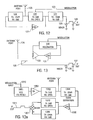
- FIG. 10 shows the baud rate adjustment loop functions in the master and slave radios.
- FIG. 11 is a block diagram of the data-path processing in the digital section including forward error correction and baud-rate adjusting word stuffer in the transmit side.
- FIG. 12 is a block diagram of a preferred embodiment of a radio front-end circuit with a single active component.
- FIG. 13 is a block diagram of another preferred embodiment of a radio front-end circuit with fewer filters, but no receive gain.
- FIG. 13A is a is a block diagram of yet another preferred embodiment of a radio front-end circuit with separated amplifiers for transmit and receive side
- FIG. 14 illustrates a varactor-tunable resonator suitable for MST implementation of the resonator in FIGS. 12 and 13 .
- FIG. 15 illustrates a filter with feed-through signal suitable for MST implementation of the filters in FIGS. 12 and 13 .
- FIG. 16 is a 3-D simulation-model for the filter in FIGS. 14 and 15 .
- FIG. 17 shows constellation diagrams for QPSK transmit and received IF before modulation cancellation.
- FIG. 18 shows the main building blocks in a radio transceiver associated with PSK-based logic-level modulation cancellation
- the invention is particularly applicable to a frequency shift keying (FSK) microwave radio and it is in this context that the invention will be described. It will be appreciated, however, that the radio and method in accordance with the invention has greater utility since its teachings may be applied to other modulation schemes and techniques as well as to other frequency domains.
- FSK frequency shift keying
- a radio assembly 15 of a preferred embodiment is depicted in FIG. 1 .
- the radio 15 includes an enclosure 1 for the electronics and antenna, a radome 2 and attached electrical and fiber optics cables 3 .
- the radio 15 is attached via a gimbals mechanism 4 to a mounting bracket 5 , which is usually attached to a wall or a pole by any typical attachment mechanism, such as a bolt.
- the gimbals mechanism may preferably include two axes 6 and 7 that allow simultaneous radio movement by the installer of the radio's azimuth and elevation until a desired pointing angle is achieved. Since a typical high-gain antenna at millimeter wave frequencies has a beam width of approximately 1.5 degrees, precise alignment up to a fraction of a degree is necessary. Since both sides of the link may possess a high-directivity antenna, electrical adjustments are very difficult, because both antennas must point at each other quite precisely before either side can receive signals of adequate strength.
- a preferred alternative in accordance with the invention to the electrical adjustment is a visual alignment mechanism. It is possible by current machining technology to manufacture the main antenna with a fraction-degree tolerance between the mechanical reference-plane and the direction of the radiated beam. Therefore, a sight-mechanism placed parallel to the antenna beam can provide adequate directional indication. A sample location 8 for a front aperture of a sight is depicted.
- FIG. 2 illustrates more details of a preferred embodiment of a sight mechanism 20 in accordance with the invention.
- the sight 20 consists of a front aperture 21 , a rear aperture 22 and a ray-bending mirror 23 , placed at the rear of the radio enclosure 1 .
- a hollow tube 25 provides environmental protection to the inside of the enclosure 1 , or an optical window is placed at the front aperture 21 .
- the bending mirror 23 allows the installer to observe the antenna sight in the limited space behind the radio enclosure and the wall behind in that the installer does not need to be behind the enclosure 1 to perform the alignment.
- the installer observes the image of the remote radio thought the sight and aligns the radio assembly with simple hand manipulation of the gimbals mechanism 4 until the remote radio is observed at the center of the sight aperture.
- the front aperture 21 diameter is selected so that the typical angular width of the aperture 21 as viewed from the observer's eye position is approximately 1.5 degrees. Precision of this angle is not critical, as the installer can visually place the remote radio in the center of the aperture 21 , regardless of width. After proper alignment is accomplished, the installer can tighten the gimbals mechanism axes mechanisms 6 , 7 and verify again the alignment optically.
- this sight mechanism is simple and low cost, several sights can be placed in the radio assembly 1 , such as in locations 9 , 10 , 11 , such that the alignment can be performed and observed from any side. Furthermore, it is possible to mount the radio assembly 1 rotated 90 degrees for cross polarization operation, if desired, by rotating the radio assembly 1 and relocating the axis 6 to a perpendicular point 12 . Thus, a plurality of sights allows easy visual alignment at any polarization.
- optical pointing devices such as gun sights
- holes in the radio structure such as one of the holes 8 , 9 , 10 , 11 .
- FIG. 3 An electrical block diagram of a preferred embodiment of a radio 30 is depicted in FIG. 3 .
- a radio link consists of two such systems facing each other at a typical distance of a few tens to a few hundreds of meters.
- each radio operates in a full duplex mode, regardless of user payload. In the full duplex mode, if the user has no information to send, an idle code is transmitted.
- the connection with a local computer and/or a communications network (not shown) is performed via an I/O port 31 which permits the digital data to/from the radio to be communicated to the local computer or communications network.
- the I/O port 31 is application-specific and can be modified for various different applications, however the preferred embodiment is best illustrated in a Gigabit-Ethernet application (GigE).
- the port 31 is either electrical or fiber optics, and an appropriate I/O processor 32 is used which is commercially available for various applications, including GigE and Sonet/SDH.
- the I/O processor 32 acts as an interface between the entity that uses the data from the radio and the radio.
- a Digital Section 33 mediates between the I/O processor 32 and a radio modem 34 .
- the digital section 33 performs functions such as buffering, framing, serial to parallel word conversion and forward error correction (FEC).
- FEC forward error correction
- the digital section 33 is also responsible for the word stuffing and de-stuffing associated with the baud rate adjustment process as described below in more detail.
- the implementation of the Digital Section 33 is straight-forward to engineers skilled in the art, using field programmable gate arrays (FPGA) or ASIC technologies so that only subsystems and processes of special significance to this Invention will be further discussed in detail below.
- FPGA field programmable gate arrays
- the modem 34 may perform various well known phase or frequency modulation operations.
- the modem 34 in accordance with the invention may perform well known frequency shift keying (FSK).
- the radio 30 includes the direct modulation of a VCO (as described below), the modem 34 sends the transmit baseband signals via a transmission line 35 directly to a radio frequency (RF) front-end 36 .
- the receive signals are sent to an interface (IF) section 37 that amplifies and filters the receive signals before the received signal is demodulated at the modem 34 .
- the radio 30 further includes a baud rate control loop 38 , related to bit timing alignment, and a modulation control loop 39 for adjusting the modulation level of the transmitted signal.
- the modem 34 may also include a well known automatic frequency control (AFC) loop 310 .
- a microcontroller 311 based on a commercially available integrated circuit (IC), performs various housekeeping tasks which include system initialization and signal conditioning tasks associated with the Baud Rate Control loop 38 .
- Other blocks which are obvious to engineers skilled in the art, are not shown. For example, a power supply and other elements are omitted from FIG. 3 .
- FIG. 4 The general principle of a digital modulation cancellation method and system in accordance with the invention is shown in FIG. 4 .
- a composite digital bit stream including user information (data) input by the I/O port 31 (See FIG. 3 ) and all of the related overhead, is generated by a transmit section 41 , which is a part of the Digital Section 33 shown in FIG. 3 .
- the binary transmit signal is delivered by a transmission line 42 to a pre-modulator 43 .
- the line 42 may be a single high-speed binary signal line (serial line) or a bus containing several parallel bit streams.
- the pre-modulator 43 a part of the modem 34 shown in FIG.
- VCO voltage controlled oscillator
- This conditioning by the pre-modulator 43 includes signal level translation, parallel to serial conversion if necessary, and low pass filtering, also known as pulse shaping.
- the signal delivered to the VCO 44 has two levels (digital logic 1 and digital logic 0) and the transitions between them, which is essentially a filtered NRZ signal.
- the resulting modulation at the output of the VCO is binary frequency shift keying (B-FSK).
- B-FSK binary frequency shift keying
- the FSK signal is described as consisting of two distinct frequencies, i.e.
- the actual modulated signal also contains transition periods, which last a fraction of a bit period and are adjusted at the pre-modulator 43 to a degree of abruptness compatible with the radio frequency allocation.
- the actual transmit spectrum is affected by these transitions and by the frequency deviation between T 0 and T 1 .
- T 0 and T 1 are set at one half the (maximum) baud rate, which is essentially Minimum Shift Keying (MSK), however other spacing can be used if the channel bandwidth allows and obtaining higher deviation at the VCO 44 is economically feasible.
- MSK Minimum Shift Keying
- the VCO 44 produces a modulated transmit signal which is fed by a transmission line or a waveguide 45 to a power junction 46 and an antenna port 47 .
- the power junction 46 consists of any suitable microwave device such as a diplexer, circulator or a power divider with a directional coupler. The choice of the particular power junction is design-specific. Some specific choices are discussed below in conjunction with FIGS. 12 , 13 and 14 .
- a receive signal arrives at the antenna port 47 and is delivered via the power junction 46 to a mixer 48 .
- An optional low-noise amplifier (LNA) (not shown) may be included.
- the frequency of the receive signal is different from the transmit frequency, thus if both the transmit signal on line 45 and the receive signal are present at the mixer 48 , a frequency difference will be generated (an If frequency) and will be delivered to an IF section 49 .
- a typical mixer 48 is a single port device, usually implemented by a diode. If the power junction 46 does not leak strong signal from the VCO output on line 45 towards the mixer port, an alternative bypass line 410 can provide the local oscillator function and the mixer 48 may be a three port unit.
- the IF section 49 receives the frequency difference signal and performs amplification and filtering.
- a conditional demodulator 415 recovers the receive bits based on the mixed signals at the IF 49 output and the transmit bits 42 .
- An example of internal structure of a conditional demodulator 415 includes an interim demodulator 411 , a delay compensator 413 and a logic gate 412 .
- the interim demodulator 411 detects the discrete frequencies of the combined IF signal similar to a conventional FSK demodulator, except that the mixing with the transmit signal may create more than two discrete frequencies, However, based on prior knowledge of the transmit binary data, the interim demodulator 411 can be controlled to monitor only two relevant frequencies at a time, as will described later, in conjunction with FIGS.
- a compensation gate 412 eliminates the effect of the transmit bits on line 42 which are properly delay compensated by a delay line 413 before being sent to the gate 412 .
- an exclusive OR (XOR) logic gate is depicted, the actual logic is specific to the choice of frequencies and modulation-type, and the proper logic can be derived from a specific truth table as is well known. If the high-speed of the digital transmission does not allow simple analog switching of sections within the demodulator 411 , the demodulator may contain multiple parallel demodulating sections, each associated with a different transmitted logic value.
- a binary FSK For example, in a binary FSK, one demodulator assumes transmitted zero and thus observes the IF signals with that assumption while another section assumes transmitted one.
- the logic gate 412 selects of the bit received by the section that assumes the actual transmitted bit, as discussed later in conjunction with FIG. 7 a .
- the received bits output from the gate 412 are delivered to a receive-digital section 414 for further processing and delivery of the payload to the I/O port.
- the output of the gate 412 is driven to a well known serializer-deserializer (SERDES) device at the digital section 414 .
- SERDES serializer-deserializer
- the timing of the transmit (TX) and receive (RX) signals need not be matched.
- transitions of the TX signal at the mixer 48 may occur in the middle of the reception of a bit, thus the bit will appear to be sliced between two logic levels at the demodulator 411 so that part of a bit may be demodulated as a zero and the other demodulated part as a one.
- the modulation correction gate 412 will still rectify the bit to the correct value, except for a glitch during the transmit bit transition.
- the glitch in the TX signal can be cleaned up with proper low pass filtering. While reception of random TX/RX timing as above is feasible, there is a degradation in bit-error performance, thus the timing correction by baud rate adjustment is provided in a preferred embodiment as described below in more detail.
- a preferred FSK frequency allocation is shown in FIG. 5 , as discussed by the following example.
- a first radio and a second radio are communicating with each other separated by some distance.
- all frequency differences between a “T” and an “R” are possible.
- T 0 R 0 For example, if a “0” is received while a “0” is transmitted (T 0 R 0 ), an IF frequency of 1.5 GHz (the difference between the frequency of the received and transmitted signals) is produced, which is marked “T 0 R 0 ” in FIG. 5 .
- T 0 R 1 Transmit a “0” and receive a “1”
- T 1 R 0 are received at 3 GHz
- T 1 R 1 is received at 1.5 GHz.
- a novel feature of this scheme is the fact that the demodulator receives only two IF frequencies, identical to a simple binary FSK receiver, thus a conventional demodulator can be used, and the only correction required is an exclusive OR (XOR) (or NXOR) operation between the “T” bit and the “R” bit after demodulation.
- XOR exclusive OR
- NXOR NXOR gate
- this frequency allocation scheme separates the transmit band from the receive band, thus allowing more freedom in the choice of the IF frequency.
- the center frequency for the local transmitter is marked “T” 601 , and for the remote transmitter “R” 602 .
- R may be 64.75 GHz and “T” may be 60.75 GHz.
- the local and remote center frequencies were identical.
- this second method is the presence of three distinct frequencies (T 1 R 0 , T 0 R 1 and T 1 R 1 /T 0 R 0 ) instead of two.
- this IF signal is a three level FSK, in which during the transmission of every TX bit, only two out of the three levels are possible.
- the third level can be switched off by a fast switching device driven by the value of the transmitted bit.
- the demodulator 70 may have three filters 71 , 72 , and 73 , which can be implemented on printed circuit materials suitable for microwave frequencies, such as Rogers Material.
- the demodulator may correspond to the demodulator 411 shown in FIG. 4 and may receive the IF unit 49 output signals as described above.
- the filter 71 represents a binary hypothesis that always exists because either T 0 R 0 or T 1 R 1 is always present and thus it is followed by a conventional envelope detector 74 (a diode in this example) and a low pass filter 75 (implemented in this example of a well known resistor and capacitor combination).
- This implementation is a non-coherent receiver.
- a coherent receiver may be used in accordance with the invention, but would be more expensive.
- T 1 R 0 is a valid hypothesis if a “1” was transmitted and filter 72 is used, while filter 73 should be included only if a “0” was transmitted.
- the filter selection can be done by an RF switch, e.g. by using Schottky diodes as is well known.
- a simple diode summing (a wire AND) of the two envelope detectors 76 and 77 of the filters 72 , 73 provides effectively simple switching with only a fraction of a dB of degradation of the radio channel noise tolerance compared with ideal complete on/off switching.
- a comparator 78 and a bit-timing “D” flip-flop or a latch 79 are the same as a conventional demodulator and operate in the same manner.
- An exclusive OR gate (XOR) 710 that corresponds to the logic gate 412 in FIG. 4 ) cancels the TX modulation. It is assumed here that bit-timing alignment is provided, otherwise the latch 79 is bypassed and low glitch reduction is provided past the gate 710 output, usually by the SERDES.
- FIG. 7 a Another embodiment of the three level FSK demodulator is depicted in FIG. 7 a .
- each IF frequency has an independent peak detectors 76 a - c and low pass filters 75 a - c so two comparators 781 , 782 are used.
- One comparator 781 examines the “Transmitted 1 ” or T 1 assumption, i.e. T 1 R 1 vs. T 1 R 0 .
- the other comparator 782 assumes zero transmitted, or T 0 R 1 vs. T 0 R 0 .
- a multiplexing gate 783 selects the right comparator output based on the value of a properly timed TX Data signal 784 . While the design of FIG. 7 a is only slightly different from FIG. 7 , the logic function is completely different (a multiplexer 783 vs. an XOR gate 710 ). While the logic function varies, the determination of the right logic function is simple, once the structure for making interim logic level decisions is chosen.
- each side transmits multi-level FSK, i.e. M-level FSK, wherein M specifies the number of discrete levels.
- FIG. 7 b A general M-FSK conditional demodulator for essentially orthogonal signals is depicted in FIG. 7 b .
- the IF signals are processed by 2M ⁇ 1 parallel circuits, which are referred to by indices from 0 through 2M2 (f 0 . . . f 2m ⁇ 2 ).
- Each circuit, such as f 0 791 includes a bandpass filter, an envelope detector and a low pass filter, similar to the channel elements 71 , 76 c 75 c depicted in FIG. 7 a .
- Each signal is controlled by an electronics ON/OF switch 794 controlled by a line 797 from a decoder 793 . The decoder is controlled based on the transmitted data signal as shown.
- the channel 791 signal is driven to a “Select Largest” circuit 795 , otherwise the switch is disabled (“OFF”) and no signal, or negligible signal level is presented to the “Select Largest” circuit 795 .
- the Decoder 793 enables M switches out of the 2M ⁇ 1, such as switches 794 , 798 .
- the logic of enabling can be described by the following convention.
- the transmitted binary word is referred by the index “i” from 0 through M ⁇ 1.
- the received binary word (yet undetected) is referred by the index “j” from 0 through M ⁇ 1.
- the IEF channels are indexed from 0 through 2M ⁇ 2, as depicted. If frequency i was transmitted, the M switches with indices from M ⁇ 1 ⁇ i through 2M ⁇ 2 ⁇ i are enabled.
- the dynamic enabling disabling of the switches demonstrates the conditional aspect of the demodulator.
- the Select Largest Section circuit 795 outputs an index from 0 through 2M ⁇ 2 (the signal with the largest index which reaches the select largest circuit) at an output bus 799 .
- This binary value from the select largest circuit is referred below as “U”.
- This unit 795 is well known in the art of digital receivers for multi-level communications and it includes comparators and logic gates.
- the Select Largest unit 795 may be designed so that the index bus 799 includes the subtraction M ⁇ 1, thus the output 795 will consist of U ⁇ M+1.
- the Select Largest section 795 performs the interim demodulation (as described above) while the adder 796 performs the transmit modulation cancellation as described above.
- FIG. 8 depicts the various control loops in the modem section 34 , which in a preferred embodiment, are implemented using analog circuits.
- the main signal path is described first.
- the transmit digital stream is output from the system FPGA as a parallel word, because commercial low-cost FPGA units are limited in digital speed and thus cannot output at the system desired rate of approximately 1.4 Gbps, which provides for a Gigabit. Ethernet traffic and overhead. Therefore, the parallel word is converted to a serial format by a SERDES transceiver 81 , which is commercially available from Texas Instruments as part number TLK2201.
- the SERDES output is converted from differential to single-ended using an analog device 82 such as a BALUN transformer.
- Low-pass filtering and amplitude adjustment are then performed by an analog circuit 83 , which is essentially the pre-modulator 43 discussed above.
- the filtering is part of the communication channel frequency response and, as mentioned above, is a compromise between short signal rise time and a bound spectral occupation wherein the optimum is selected based on the application. In the 60 GHz band, a rise time of approximately 0.1 of a bit-period is preferred.
- the amplitude of the signal at this point is affecting the deviation of the transmitted signal at a VCO 85 .
- the signal is then fed into a DC level adjust 84 that is used for fine-tuning the transmitted frequency at the VCO 85 .
- the IF signal from a receive mixer 86 is amplified by an low noise amplifier 87 (not to be confused with a radio front-end LNA if in use), a filter 88 and further amplifiers 89 that may saturate, given a constant-envelope signal.
- the signal is then FSK-detected by an FSK detector/demodulator 810 , such as the circuit shown in FIGS. 7 and 7 a , and after a comparator 811 (the same comparator 78 as in FIG. 7 ), sent to the SERDES.
- the modulation cancellation XOR function and flip-flop timing occurs in the Digital Section.
- the Automatic Frequency Control (AFC) function as described above is performed by an FM discriminator circuit 812 (a frequency deviation detector circuit), followed by the conventional elements of an AFC loop.
- the discriminator function 812 requires special attention with regards to the IF signals received in accordance with this invention.
- a conventional FM discriminator is sufficient, and tracking the center frequency of one of the three signals, such as T 1 R 0 would suffice.
- T 1 R 0 a frequency increase of the transmitter, i.e. T 0 and T 1 move higher in FIG.
- AFC 5 would cause a split of each IF frequency, since T 0 R 0 would decrease and T 1 R 1 would increase, creating ambiguity in the AFC loop.
- This situation can be corrected by two main methods.
- One method uses the transmitted bits as indicators of the frequency shift direction, thus it includes multiplying the discriminator 812 output by the polarization of the transmitted bit, using a bipolar modulator 813 to replace the direct connection 814 to the following stages.
- Another method is based on using the transmitted bits to switch off the discriminator output 814 when a binary “1” is transmitted, to track “T 0 ” instances only, or binary “0” to track “T 1 ” instances.
- a completely different method is based on the transmitted bits.
- Yet another method can be used for AFC in FIG. 5 .
- a conventional discriminator 812 is used, however the discriminator center frequency is located slightly off center to the desired signal spectral line. For example, if the spectral center T 0 R 0 in FIG. 5 is used as the reference and the desired frequency is 1.5 GHz, then the discriminator 812 covers the range 1.2 to 1.5 GHz, and the control loop adjusts the system frequency to be in the higher end, i.e. 1.5 GHz up to acceptable tolerance.
- Such loop has ambiguity in the increase/decrease sense because if the frequency (To and T 1 ) is too low, then T 1 R 1 will veer into the discriminator band and the loop should increase the VCO 85 center frequency. If the frequency is too high, T 0 R 0 will veer down and the VCO 85 should increase in frequency. Therefore the AFC loop should include loop polarity search.
- the whole link-wide frequency control is obtained as follows.
- the two radios in the link are referred to as “AFC-master” and “AFC-slave”.
- the choice of master and slave is arbitrary and not necessarily related to which radio is termed “master” or “slave” for other purposes.
- the AFC-master VCO 85 is driven by a DC voltage that represents the center frequency. This center frequency is largely determined by a resonator inside the VCO 85 circuit, as will be described in conjunction with FIG. 12 .
- This DC voltage can be provided by the Digital section via a D/A port 815 , thus allowing optional center frequency calibration over temperature.
- the AFC loop in the AFC-slave performs the local AFC function, thus tracking the center frequency of the AFC-master.
- the signal deviation can be permanently set in production, without the need for close loop control. If a close loop control is desired for better accuracy, the deviation is controlled by monitoring the spectral content off-center in one of the IF frequencies.
- a frequency discriminator 812 senses the spectral content and a control loop adjusted by the transmit signal gain amplifier 83 . Since the deviation reading and the discriminator 812 could be also affected by off-center tuning of the VCO 85 in both sides of the link, the deviation loop time constant is set at a much slower response time than the AFC. For example, the AFC time constant is set to 0.001 sec, and the deviation control to 0.01 sec. This loop has a drawback, as the discriminator 812 reading is affected by the deviation of both radios.
- the feedback signal is a sum of the “T” deviation and the “R” deviation.
- the local radio can extract feedback based on the local deviation only, as follows.
- Discriminator 812 is centered at the signal T 0 R 1 in FIG. 6 .
- the frequency reading of this discriminator is proportional to the sum of the “T” deviation and the “R” deviation.
- a discriminator 820 is centered on the frequencies T 0 R 0 /T 1 R 1 in FIG. 6 , and the bipolar modulator 813 is used as above.
- the output of the modulator 813 is proportional to the difference of deviations.
- V 812 K 1( DT+DR )
- V 813 K 2( DT ⁇ DR )
- K 1 and K 2 are design-related constants that are known in production with much higher accuracy than the actual deviation, because they are set by the discriminators and modulators design, rather than the VCO tuning circuit which is less accurate in gain variation.
- the third loop shown in FIG. 8 is a baud rate control loop (shown in FIG. 3 as element 38 ), may include a Rate Mismatch Detector 817 , an Integrator 818 and a Microprocessor 819 .
- the principle of detecting baud rate mismatch is illustrated in FIG. 9 .
- the signals depicted are referred to the comparator 811 output in FIG. 8 . If both TX and RX sides coincide in bit timing at the mixer 86 , the waveform 91 has no bit, transition ambiguities.
- the power spectrum 92 of such bit stream would have a null at a frequency equal to the baud rate about a point marked “F 2 ”.
- the spectrum 94 will widen, fill the null at F 2 and reduce its main lobe amplitude at frequencies below F 2 , such as the frequency marked “F 1 ”. It should be emphasized that as the baud rate increases, the null position F 2 increases too, however the change in location of the null is less than 1%, while the main spectral lobe widens by up to 100%, thus the null position F 2 is essentially fixed.
- the Rate Mismatch Detector 817 includes a filter (such as one formed by a well known inductor and capacitor combination) and an envelope detector, such as a diode.
- the filter is a band pass filter at frequency F 2 with a wide-band sufficiently to accommodate the approximately 1% change in baud rate.
- the filter can be a band pass centered at a frequency F 1 substantially lower than F 2 . If an F 2 filter is implemented, the goal of the control loop is to minimize the spectral content detected in band. If the F 1 filter is implemented, or any low pass filter with cutoff below F 2 , then the goal is to maximize spectral content within the filter.
- a search process in the Microprocessor 819 is used. This method includes the steps of changing (increasing or decreasing) the baud rate, monitoring the detector 817 envelope response to that change and initiating more changes to a direction that is observed to be moving towards the desired goal.
- baud rate 1/(2 ⁇ path delay)
- Pulseth delay is the propagation delay from the RF front-end mixing point at one radio to same point in the opposite radio.
- the shortest radio link distance has the shortest path delay, thus it requires the highest frequency addition and the transceiver design assumes a minimum distance, Dmin, for setting Fadd.
- the whole-link operation of the baud rate control loop is shown in FIG. 10 .
- the radios are arbitrarily assigned the terms “Master” and “Slave” for baud rate purpose as shown, regardless of master/slave assignments for other purposes.
- the baud rate is controlled based on the following process.
- the first part of the process is a search and capture phase that brings both side to a near-optimum match. A 90% match in timing is sufficiently good as a capture goal.
- the Master sets initially an arbitrary baud rate by a VCO 101 , which determines the baud rate for the transmitted signal 102 . This initial baud rate may equal Fmin+0.5 Fadd.
- the Slave then receives the Master signal 102 , and attempts to phase lock to it by a SERDES 103 built in PLL. If successful, the SERDES 103 tracks the receive clock frequency 105 and derives its own transmit clock 104 from the received clock 105 . The receive timing will most likely not match the Slave timing and the Slave will increment the local clock frequency with an attempt to achieve lock. While the slave performs such increments at the rate of 1000 increments per second, for example, the Master perform a similar search at the rate of about 100 increments per second. Within 0.1 Seconds, the Master has tried 10 increments, and for each Master increment the Slave has tried 10 increments, thus one of these 100 combinations should be within 1/10 th of each other thus meeting the capture goal.
- the Slave Upon lock, the Slave simply tracks the receive clock 105 by the transmit VCO 104 .
- the frequency incrementing, lock condition recognition and switching to tracking mode are all performed by a microprocessor 106 .
- a Master microprocessor 107 also enters tracking mode based on the output of a Rate Mismatch Detector 108 . Since the propagation delay remains fixed, subject only to occasional extreme weather changes or high-rise building swing, once a rate is determined, the microprocessor 107 can store the desired rate in memory and track changes slowly.
- FIG. 11 The overall digital signal transmission block diagram is shown in FIG. 11 .
- a digital payload 111 such as Gigabit Ethernet traffic, is input to a well known elastic buffer 112 . If no traffic exists at the system input, the system I/O section 32 (See FIG. 3 ) generates idle codes, which replace the payload 111 .
- An overhead stuffer 113 is driven by a baud rate clock signal 114 . The stuffer 113 injects a stuff-word whenever the elastic buffer 112 is less than half full based on a half-full flag as shown.
- the stuff word can be any arbitrary word, just as commonly done by well-known protocols such as HDLC, a preferred alternative is to use a word that is not in the vocabulary of the normal payload, thus is unique for the purpose of stuffing.
- the payload 111 can be organized as bytes.
- the payload may also contain control-words, which are represented by a byte with an additional “control” bit designation 117 wherein the control bit is propagated in parallel to the word via the various building blocks.
- the words at the stuffer 113 output are interrupted periodically to inject a frame overhead by a framer 115 .
- the frame overhead can be of tow words, also unique.
- a commercially available coding scheme is preferred.
- SERDES devices for GigE applications recognize 10-bit words including payloads of 8-bit in which two overhead bits indicate “data” and other 10-bit control codes. It is convenient to allocate a frame overhead based on these overhead codes, using codes not commonly found in normal LAN traffic. To facilitate processing of those 10-bit words, an industry standard 8 b / 10 b code converter 118 is used. The extra bits guarantee significant number of 0 to 1 transitions per each word to reduce the risk of synchronization loss. Finally, a forward error correction 116 block code overhead is added.
- the transmission frame may include 2 frame overhead words, 186 payload and stuff words, and 16 error check words.
- the above example may represent a Reed Solomon block code RS( 204 , 188 ) over a Galois Field GF( 256 ).
- the receive side performs the opposite operations to those of FIG. 11 , as familiar to engineers skilled in the art of digital communications.
- some large system blocks, such as the Reed Solomon Decoder may still be too slow to process the entire traffic.
- block interleaving may be used in transmission and reception as desired.
- four Reed Solomon decoders may run in parallel, such that received frames are sent in a round-robin cycles to each decoder.
- Such techniques are well known to engineers skilled in the art of digital system design.
- FIG. 12 A preferred embodiment block diagram of such an RF front-end is shown in FIG. 12 , based on the frequency arrangement of FIG. 6 .
- the system performs three amplifier-related functions with a single active amplifier.
- the amplifier a commercially available low-noise amplifier (LNA) 121 , is utilized in this circuit as an oscillator, a transmitter and a receiver.
- the oscillator function is accomplished by a resonator 122 in a feedback loop around the amplifier 121 .
- LNA low-noise amplifier
- the resonator 122 is frequency-tuned by the modulation signal 123 , using a varactor diode coupled to the resonator 122 .
- a filter 124 attenuates the transmit frequency only slightly, as indicated by the symbol Tx: ⁇ 10 dB, i.e. 10 dB loss at the transmission frequency. This attenuation enables most of the oscillator energy to propagate to the antenna port 125 , thus producing near maximum transmit power.
- the received signal at the antenna port 125 propagates via the filter 124 to the LNA 121 and is thus amplified.
- the amplified receive-signal is sent to a mixer 126 via a filter 127 that intentionally leaks part of the transmit signals too. This leaked signal is sufficiently strong to mix with the received signal at the mixer 126 and produce IF output via a low-pass filter 128 . If needed, the mixer diode 126 can be forward biased slightly to improve sensitivity.
- FIG. 13 While the preferred embodiment disclosed in FIG. 12 provides both receive gain and transmit power, another embodiment is disclosed in FIG. 13 for further reduction of the number of microwave components, and for suitability to both frequency arrangements of FIGS. 5 and 6 .
- the circuit in FIG. 13 includes an amplifier 131 , a modulated resonator 132 and a Wilkinson power divider 133 that splits the amplifier output to the feedback loop via the resonator 132 and an antenna port 134 .
- a directional coupler 135 picks up a small fraction of the transmitted signal, e.g. 1/10 th of the power, and the majority of the received signal. This coupler 135 feeds the signals to the mixer 136 and low pass filter 137 .
- the mixer diode 136 may be slightly forward biased for better sensitivity.
- This embodiment does not provide receive signal gain at the radio frequency that was provided by the other preferred embodiment in FIG. 12 , thus some reduction in receive noise figure performance is expected, however the simplicity of this structure may justify it in some applications.
- the amplifier 131 can be replaced by a Gunn diode or a similar single port device, thus providing an option of increased output power and cost-reduction.
- FIG. 13A For added performance at some increased cost, another embodiment of the RF front end is shown in FIG. 13A .
- the transmit and receive paths are further separated, allowing independent choice of components for each direction.
- a VCO 1301 On the transmit side, a VCO 1301 is followed by an optional power amplifier 1302 , to provide higher transmit power.
- a diplexer is formed, consisting of a transmit side filter 1303 and receive filter 1304 .
- the receive side signal path is followed by an LNA 1305 , and then the signals are split by receive filter 1306 and transmit filter 1312 to feed a balanced mixer 1307 .
- the pair of filters 1306 and 1312 form a diplexer which is similar to the pair of filters 13033 and 1304 , thus further cost savings are achieved by using essentially the same diplexer design for both diplexer functions, where both diplexers are either identical or include simple changes such as metallization mask change.
- the demand from the receive filter 1304 in rejecting transmit signal is higher than the equivalent filter 124 in FIG. 12 , however it is still much less than a diplexer in a conventional transceiver with no modulation cancellation.
- the use of a balanced mixer is preferred because a balanced mixer reduces the presence of unwanted harmonics of the transmit modulation present at the mixer inputs, especially if the transmitted signal has accumulated FM to AM conversion while propagating via various filters between the VCO 1301 and the mixer 1307 . While this embodiment uses more components, it allows easier separations of the transmitter modulation input signal 1310 from the IF signal 1311 than the two previous embodiments.
- FIG. 14 shows a top view a tunable resonator 140 , with the metal cap removed to exposed the inside structure.
- a resonating element 141 is printed on a membrane suspended above a ground plane 142 and attached to a substrate 149 , such as high resistivity silicon.
- Two electrodes 143 and 144 provide input/output ports, and are connected by a transmission line 145 , which is loaded by the resonator 141 .
- a varactor chip diode 146 is coupled to the resonator 141 and a ground-via 147 is connected to a ground conductor 148 .
- a DC voltage to tune the diode is provided via one of the ports 143 , 144 , superimposed to the RF signal.
- the dimensions of the entire die of FIG. 14 for a 60 GHz application are approximately 3 mm by 3.5 mm, as desired for small size.
- a filter geometry is shown in FIG. 15 .
- the structure is identical to that of FIG. 14 , with a different geometry that provides the desired frequency response. This structure can be used for the filters 124 and 127 in FIG. 12 .
- the die dimensions are 2.5 ⁇ 3.1 mm.
- FIG. 16 is a simulation model for the filter of FIG. 15 . This model illustrates a perspective view of the silicon 161 and ground planes 162 , 163 required for analyzing the filter performance.
- a complete RF front-end including the above filters, resonator and amplifier may be implemented on a substrate of about 12 ⁇ 12 mm. This small size allows mounting of this circuit directly at the feed point of a high gain antenna, thus further reducing signal losses and cost.
- the modulation cancellation techniques disclosed above used frequency modulation (FSK), other modulation schemes can be used, although constant-envelope is preferred.
- FSK frequency modulation
- QPSK Quaternary Phase Shift Keying
- the radio block diagram as shown in FIGS. 3 and 4 is unchanged, however the VCO 85 in FIG. 8 is changed to a QPSK-modulated oscillator, as known to engineers skilled in the art of microwave radio circuit design.
- the demodulators are replaced by QPSK demodulators too.
- the modulation may be coherent or differential. For coherent modulation, a constellation 171 in FIG.
- the IF 172 is shown as an example, with a sample of bit value allocation (00, 01 etc.).
- the same constellation is used for both sides of the link.
- the transmitted symbol streams in both sides include overhead codes, which help the establishment of phase synchronization as customary in coherent QPSK techniques.
- the combined transmit/receive phases in the IF 172 are still QPSK, however the constellation points represent the phase difference between the transmitted received phases.
- the “R” frequency is higher than the “T” frequency, such as the band arrangement “T” 601 and “R” 602 in FIG. 6 .
- the IF phase 172 will be the difference between T and R 171 .
- Phase is measured counter clockwise from the “I” axis.
- the QPSK transmission could also be differential, simplifying the receiver structure at the slight expense of bit error rate.
- the constellation 171 in FIG. 17 is still valid, except that each angle position represents the increment from the previous symbol.
- the IF interim demodulator is differential and the logic modulation cancellation is still an addition modulo 4 .
- FIG. 18 Similar to the building blocks in FIG. 4 , a PSK transceiver is depicted in FIG. 18 . The only differences are a PSK modulator 184 replacing the FSK modulator 44 and a Full Adder 1812 replacing the XOR gate 412 .
Abstract
Description
T1R0=4 GHz, T0R0=T1R1=5.5 GHz and T0R1=7 GHz.
j=U−M+1+i
V812=K1(DT+DR)
V813=K2(DT−DR)
DT=V812/K1+V813/K2
Fadd=1/(2×path delay)
Claims (5)
Priority Applications (1)
| Application Number | Priority Date | Filing Date | Title |
|---|---|---|---|
| US10/987,819 US8311082B2 (en) | 2002-12-20 | 2004-11-12 | Wideband digital radio with transmit modulation cancellation |
Applications Claiming Priority (3)
| Application Number | Priority Date | Filing Date | Title |
|---|---|---|---|
| US43583902P | 2002-12-20 | 2002-12-20 | |
| US10/423,154 US6937666B2 (en) | 2002-12-20 | 2003-04-24 | Wideband digital radio with transmit modulation cancellation |
| US10/987,819 US8311082B2 (en) | 2002-12-20 | 2004-11-12 | Wideband digital radio with transmit modulation cancellation |
Related Parent Applications (1)
| Application Number | Title | Priority Date | Filing Date |
|---|---|---|---|
| US10/423,154 Continuation US6937666B2 (en) | 2002-12-20 | 2003-04-24 | Wideband digital radio with transmit modulation cancellation |
Publications (2)
| Publication Number | Publication Date |
|---|---|
| US20050094718A1 US20050094718A1 (en) | 2005-05-05 |
| US8311082B2 true US8311082B2 (en) | 2012-11-13 |
Family
ID=32599996
Family Applications (3)
| Application Number | Title | Priority Date | Filing Date |
|---|---|---|---|
| US10/423,154 Expired - Lifetime US6937666B2 (en) | 2002-12-20 | 2003-04-24 | Wideband digital radio with transmit modulation cancellation |
| US10/843,843 Expired - Fee Related US7469128B2 (en) | 2002-12-20 | 2004-05-11 | Wideband digital radio with transmit modulation cancellation |
| US10/987,819 Expired - Fee Related US8311082B2 (en) | 2002-12-20 | 2004-11-12 | Wideband digital radio with transmit modulation cancellation |
Family Applications Before (2)
| Application Number | Title | Priority Date | Filing Date |
|---|---|---|---|
| US10/423,154 Expired - Lifetime US6937666B2 (en) | 2002-12-20 | 2003-04-24 | Wideband digital radio with transmit modulation cancellation |
| US10/843,843 Expired - Fee Related US7469128B2 (en) | 2002-12-20 | 2004-05-11 | Wideband digital radio with transmit modulation cancellation |
Country Status (3)
| Country | Link |
|---|---|
| US (3) | US6937666B2 (en) |
| AU (1) | AU2003301169A1 (en) |
| WO (1) | WO2004059852A2 (en) |
Cited By (3)
| Publication number | Priority date | Publication date | Assignee | Title |
|---|---|---|---|---|
| US20110064415A1 (en) * | 2008-05-13 | 2011-03-17 | Williams Brett A | Radio frequency photonic transceiver |
| US9634873B1 (en) * | 2016-01-25 | 2017-04-25 | National Chiao Tung University | BPSK demodulator |
| US9906386B1 (en) | 2017-01-13 | 2018-02-27 | Cypress Semiconductor Corporation | Frequency estimation, correction and noise suppression for modems |
Families Citing this family (45)
| Publication number | Priority date | Publication date | Assignee | Title |
|---|---|---|---|---|
| US7831305B2 (en) | 2001-10-15 | 2010-11-09 | Advanced Neuromodulation Systems, Inc. | Neural stimulation system and method responsive to collateral neural activity |
| WO2003026738A1 (en) * | 2001-09-28 | 2003-04-03 | Northstar Neuroscience, Inc. | Methods and apparatus for electrically stimulating cells implanted in the nervous system |
| US20040229647A1 (en) * | 2003-05-14 | 2004-11-18 | Mr. George Simmons | Cellular Communication Computer Intranet Internet Interface Design |
| US7483747B2 (en) | 2004-07-15 | 2009-01-27 | Northstar Neuroscience, Inc. | Systems and methods for enhancing or affecting neural stimulation efficiency and/or efficacy |
| US20060035608A1 (en) * | 2004-08-11 | 2006-02-16 | Interdigital Technology Corporation | Method and system for using angular hopping in wireless communication systems |
| US7738853B2 (en) * | 2004-10-29 | 2010-06-15 | Antone Wireless Corporation | Low noise figure radiofrequency device |
| US7228154B2 (en) * | 2004-11-03 | 2007-06-05 | Sony Corporation | Method and system for processing wireless digital multimedia |
| US8364185B2 (en) * | 2005-04-18 | 2013-01-29 | Samsung Electronics Co., Ltd. | Method and system for synchronizing a clock for an adjacent network to a clock for an overlay network |
| US7512391B2 (en) * | 2005-05-24 | 2009-03-31 | Freescale Semiconductor, Inc. | Self-aligning resonator filter circuit and wideband tuner circuit incorporating same |
| WO2007038777A2 (en) * | 2005-09-29 | 2007-04-05 | Techwell, Inc. | Carrier phase independent symbol timing recovery methods for vsb receivers |
| US9059866B2 (en) * | 2005-12-30 | 2015-06-16 | Remec Broadband Wireless Holdings, Inc. | Digital microwave radio system and method with encryption |
| US8711888B2 (en) * | 2005-12-30 | 2014-04-29 | Remec Broadband Wireless Llc | Digital microwave radio link with adaptive data rate |
| US8731007B2 (en) | 2005-12-30 | 2014-05-20 | Remec Broadband Wireless, Llc | Digital microwave radio link with a variety of ports |
| US7512395B2 (en) * | 2006-01-31 | 2009-03-31 | International Business Machines Corporation | Receiver and integrated AM-FM/IQ demodulators for gigabit-rate data detection |
| KR100744456B1 (en) * | 2006-04-10 | 2007-08-01 | 인하대학교 산학협력단 | M-ary orthogonal/balanced uwb-transmitted reference system |
| US7576687B2 (en) * | 2007-07-17 | 2009-08-18 | Infineon Technologies Ag | RF front-end circuitry with reduced DC offset |
| US20080208291A1 (en) * | 2006-10-24 | 2008-08-28 | Northstar Neuroscience, Inc. | Frequency shift keying (fsk) magnetic telemetry for implantable medical devices and associated systems and methods |
| TWI338971B (en) * | 2007-09-10 | 2011-03-11 | Wistron Corp | Electronic device capable of identifying external antenna and related external antenna module |
| KR101439371B1 (en) * | 2007-12-03 | 2014-09-11 | 삼성전자주식회사 | Method and apparatus receiver for transmit signal tracking and rejection in wireless communication system |
| US7898364B2 (en) * | 2007-12-11 | 2011-03-01 | General Dynamics Advanced Information Systems, Inc. | System and method for using MEMS filter bank |
| JP4465725B2 (en) * | 2008-04-04 | 2010-05-19 | 株式会社デンソー | Liquid concentration measuring device |
| US7898497B2 (en) * | 2008-10-01 | 2011-03-01 | Andrew Llc | Enclosed reflector antenna mount |
| EP2356750A1 (en) * | 2008-11-14 | 2011-08-17 | Intellon Corporation | Transmission suppression |
| JP5608140B2 (en) * | 2011-03-15 | 2014-10-15 | オムロンオートモーティブエレクトロニクス株式会社 | Transmitting apparatus and transmitting method |
| TWI500256B (en) * | 2011-05-25 | 2015-09-11 | Realtek Semiconductor Corp | Circuit and method for detecting oscillating frequency drift |
| US8942562B2 (en) * | 2011-05-31 | 2015-01-27 | A Optix Technologies, Inc. | Integrated commercial communications network using radio frequency and free space optical data communication |
| US8837564B2 (en) * | 2011-10-14 | 2014-09-16 | Broadcom Corporation | Multi gigabit modem for mmWave point to point links |
| EP2600544B1 (en) | 2011-11-30 | 2014-10-15 | Telefonaktiebolaget L M Ericsson (publ) | Technique for crosstalk reduction |
| CN104488136A (en) * | 2012-06-01 | 2015-04-01 | 伍比克网络公司 | Automatic antenna pointing and stabilization system and method thereof |
| US8750427B1 (en) * | 2012-11-16 | 2014-06-10 | Honeywell International Inc. | Apparatus and method for demodulation of FSK signals |
| DE102014104524B4 (en) | 2013-10-02 | 2017-07-06 | Silicon Laboratories Inc. | Receiver capable of detecting frequency deviations and methods therefor |
| US9397673B2 (en) | 2014-04-23 | 2016-07-19 | Telefonaktiebolaget L M Ericsson (Publ) | Oscillator crosstalk compensation |
| US9407274B2 (en) | 2014-04-29 | 2016-08-02 | Telefonaktiebolaget L M Ericsson (Publ) | Local oscillator interference cancellation |
| TWI533608B (en) * | 2014-06-30 | 2016-05-11 | 友達光電股份有限公司 | Data receiver and data receiving method thereof |
| US9813266B2 (en) * | 2014-07-28 | 2017-11-07 | Benjamin Kim | Distributed combined junctional transformer |
| US9257999B1 (en) * | 2014-08-01 | 2016-02-09 | Telefonaktiebolaget L M Ericsson (Publ) | Compensating for a known modulated interferer to a controlled oscillator of a phase-locked loop |
| US9450623B2 (en) * | 2014-09-19 | 2016-09-20 | Qualcomm Incorporated | Noise canceler for use in a transceiver |
| CN106161309B (en) * | 2015-03-27 | 2020-04-24 | 恩智浦美国有限公司 | Method for demodulating frequency shift keying modulated input signal and demodulator |
| US10484095B2 (en) * | 2017-06-15 | 2019-11-19 | The Aerospace Corporation | Communications relay satellite with a single-axis gimbal |
| US10411319B2 (en) * | 2017-09-29 | 2019-09-10 | The Government Of The United States Of America, As Represented By The Secretary Of The Navy | Bandstop filters with power-dependent stopband attenuation |
| CN113765648B (en) * | 2020-06-01 | 2023-03-21 | 华为技术有限公司 | Full-duplex communication method, device and system |
| US11251822B1 (en) * | 2020-07-23 | 2022-02-15 | Xilinx, Inc. | Software defined radio (SDR) filter relaxation technique for multiple-input and multiple-output (MIMO) and large antenna array (LAA) applications |
| US11791973B2 (en) * | 2020-09-24 | 2023-10-17 | Apple Inc. | Full-duplex electrical balanced duplexer |
| TWI744069B (en) | 2020-11-03 | 2021-10-21 | 立積電子股份有限公司 | Rf amplifier apparatus |
| US11558120B1 (en) * | 2021-09-30 | 2023-01-17 | United States Of America As Represented By The Administrator Of Nasa | Method for deskewing FPGA transmitter channels directly driving an optical QPSK modulator |
Citations (31)
| Publication number | Priority date | Publication date | Assignee | Title |
|---|---|---|---|---|
| US4520474A (en) | 1983-12-05 | 1985-05-28 | Motorola, Inc. | Duplex communication transceiver with modulation cancellation |
| US5036299A (en) | 1990-06-22 | 1991-07-30 | California Institute Of Technology | Method and apparatus for reducing microwave oscillator output noise |
| US5241566A (en) | 1988-12-13 | 1993-08-31 | E-Systems, Inc. | Full duplex FSK system |
| US5436930A (en) | 1993-06-14 | 1995-07-25 | At&T Corp. | Simultaneous analog and digital communications with a selection of different signal point constellations based on signal energy |
| US5440585A (en) | 1993-06-14 | 1995-08-08 | At&T Corp. | Applications of simultaneous analog and digital communication |
| US5446762A (en) * | 1989-08-25 | 1995-08-29 | Matsushita Electric Industrial Co., Ltd. | Data demodulation circuit for FSK modulated RF signal receiver providing wide-band 90° baseband phase shifting |
| US5448555A (en) | 1993-06-14 | 1995-09-05 | At&T Corp. | Simultaneous analog and digital communication |
| US5463660A (en) * | 1993-08-31 | 1995-10-31 | Oki Electric Industry Co., Ltd. | Block-spreading code-division multiple-access demodulator with improved interference cancellation |
| US5537441A (en) | 1993-06-14 | 1996-07-16 | At&T Corp. | Controlled simultaneous analog and digital communication |
| US5537436A (en) | 1993-06-14 | 1996-07-16 | At&T Corp. | Simultaneous analog and digital communication applications |
| US5844944A (en) | 1993-06-14 | 1998-12-01 | Paradyne Corporation | Simultaneous analog and digital communication using partitioning of bits into words |
| US5881047A (en) | 1993-06-14 | 1999-03-09 | Paradyne Corporation | Simultaneous analog and digital communication with improved phase immunity |
| US6018644A (en) | 1997-01-28 | 2000-01-25 | Northrop Grumman Corporation | Low-loss, fault-tolerant antenna interface unit |
| US6151354A (en) | 1997-12-19 | 2000-11-21 | Rockwell Science Center | Multi-mode, multi-band, multi-user radio system architecture |
| US6265948B1 (en) | 1999-12-20 | 2001-07-24 | Agere Systems Guardian Corp. | Image rejection in logic-based architecture for FSK modulation and demodulation |
| US6282248B1 (en) | 1998-07-14 | 2001-08-28 | Agere Systems Guardian Corp. | Variable baud rate demodulator |
| US20020015206A1 (en) * | 2000-08-03 | 2002-02-07 | Farhad Hakimi | WDM system that uses nonlinear temporal gratings |
| US20020046276A1 (en) * | 2000-07-06 | 2002-04-18 | Coffey Aedan Diarmuid Cailean | Fibre channel diagnostics in a storage enclosure |
| US20020067755A1 (en) * | 2000-12-04 | 2002-06-06 | Michael Perkins | Integrated QPSK/FSK demodulator |
| US20020122503A1 (en) * | 2001-03-01 | 2002-09-05 | Agazzi Oscar E. | Digital signal processing based de-serializer |
| US20020129379A1 (en) * | 1999-12-13 | 2002-09-12 | Levinson Frank H. | System and method for transmitting data on return path of a cable television system |
| US20020193067A1 (en) | 2001-04-26 | 2002-12-19 | Cowley Nicholas Paul | Radio frequency interface |
| US20030081700A1 (en) | 2001-10-25 | 2003-05-01 | Koninklijke Philips Electronics N.V. | Apparatus and method for using training sequences to estimate timing error in a digital signal receiver |
| US20030110509A1 (en) * | 1999-12-13 | 2003-06-12 | Levinson Frank H. | Cable television return link system with high data-rate side-band communication channels |
| US20030154495A1 (en) * | 2002-02-12 | 2003-08-14 | Finisar Corporation | Data rate compression device for cable television return path using bandpass puncturing |
| US6741643B1 (en) * | 1998-04-15 | 2004-05-25 | Telecommunications Research Laboratories | Asymmetric equalization system for data transmission |
| US20040136711A1 (en) * | 1999-09-13 | 2004-07-15 | Ciena Corporation | Optical fiber ring communication system |
| US6798784B2 (en) * | 2001-06-04 | 2004-09-28 | Caux Networks, Inc. | Concurrent switching of synchronous and asynchronous traffic |
| US6879663B2 (en) * | 2003-06-13 | 2005-04-12 | International Business Machines Corporation | Method and structure for diagnosing problems on a DSL device |
| US7184466B1 (en) * | 2002-09-12 | 2007-02-27 | Xilinx, Inc. | Radio frequency data conveyance system including configurable integrated circuits |
| US20110013911A1 (en) * | 1995-05-11 | 2011-01-20 | Alexander Stephen B | High-speed optical transponder systems |
Family Cites Families (2)
| Publication number | Priority date | Publication date | Assignee | Title |
|---|---|---|---|---|
| JPS5380906A (en) * | 1976-12-27 | 1978-07-17 | Oki Electric Ind Co Ltd | Frequency converter |
| KR100186753B1 (en) * | 1996-08-24 | 1999-05-15 | 삼성전자주식회사 | Radio transmit and receive system |
-
2003
- 2003-04-24 US US10/423,154 patent/US6937666B2/en not_active Expired - Lifetime
- 2003-12-19 AU AU2003301169A patent/AU2003301169A1/en not_active Abandoned
- 2003-12-19 WO PCT/US2003/040712 patent/WO2004059852A2/en not_active Application Discontinuation
-
2004
- 2004-05-11 US US10/843,843 patent/US7469128B2/en not_active Expired - Fee Related
- 2004-11-12 US US10/987,819 patent/US8311082B2/en not_active Expired - Fee Related
Patent Citations (32)
| Publication number | Priority date | Publication date | Assignee | Title |
|---|---|---|---|---|
| US4520474A (en) | 1983-12-05 | 1985-05-28 | Motorola, Inc. | Duplex communication transceiver with modulation cancellation |
| US5241566A (en) | 1988-12-13 | 1993-08-31 | E-Systems, Inc. | Full duplex FSK system |
| US5446762A (en) * | 1989-08-25 | 1995-08-29 | Matsushita Electric Industrial Co., Ltd. | Data demodulation circuit for FSK modulated RF signal receiver providing wide-band 90° baseband phase shifting |
| US5036299A (en) | 1990-06-22 | 1991-07-30 | California Institute Of Technology | Method and apparatus for reducing microwave oscillator output noise |
| US5537441A (en) | 1993-06-14 | 1996-07-16 | At&T Corp. | Controlled simultaneous analog and digital communication |
| US5440585A (en) | 1993-06-14 | 1995-08-08 | At&T Corp. | Applications of simultaneous analog and digital communication |
| US5448555A (en) | 1993-06-14 | 1995-09-05 | At&T Corp. | Simultaneous analog and digital communication |
| US5537436A (en) | 1993-06-14 | 1996-07-16 | At&T Corp. | Simultaneous analog and digital communication applications |
| US5844944A (en) | 1993-06-14 | 1998-12-01 | Paradyne Corporation | Simultaneous analog and digital communication using partitioning of bits into words |
| US5859877A (en) | 1993-06-14 | 1999-01-12 | Paradyne Corporation | Simultaneous analog and digital communication using fractional rate encoding |
| US5881047A (en) | 1993-06-14 | 1999-03-09 | Paradyne Corporation | Simultaneous analog and digital communication with improved phase immunity |
| US5436930A (en) | 1993-06-14 | 1995-07-25 | At&T Corp. | Simultaneous analog and digital communications with a selection of different signal point constellations based on signal energy |
| US5463660A (en) * | 1993-08-31 | 1995-10-31 | Oki Electric Industry Co., Ltd. | Block-spreading code-division multiple-access demodulator with improved interference cancellation |
| US20110013911A1 (en) * | 1995-05-11 | 2011-01-20 | Alexander Stephen B | High-speed optical transponder systems |
| US6018644A (en) | 1997-01-28 | 2000-01-25 | Northrop Grumman Corporation | Low-loss, fault-tolerant antenna interface unit |
| US6151354A (en) | 1997-12-19 | 2000-11-21 | Rockwell Science Center | Multi-mode, multi-band, multi-user radio system architecture |
| US6741643B1 (en) * | 1998-04-15 | 2004-05-25 | Telecommunications Research Laboratories | Asymmetric equalization system for data transmission |
| US6282248B1 (en) | 1998-07-14 | 2001-08-28 | Agere Systems Guardian Corp. | Variable baud rate demodulator |
| US20040136711A1 (en) * | 1999-09-13 | 2004-07-15 | Ciena Corporation | Optical fiber ring communication system |
| US20020129379A1 (en) * | 1999-12-13 | 2002-09-12 | Levinson Frank H. | System and method for transmitting data on return path of a cable television system |
| US20030110509A1 (en) * | 1999-12-13 | 2003-06-12 | Levinson Frank H. | Cable television return link system with high data-rate side-band communication channels |
| US6265948B1 (en) | 1999-12-20 | 2001-07-24 | Agere Systems Guardian Corp. | Image rejection in logic-based architecture for FSK modulation and demodulation |
| US20020046276A1 (en) * | 2000-07-06 | 2002-04-18 | Coffey Aedan Diarmuid Cailean | Fibre channel diagnostics in a storage enclosure |
| US20020015206A1 (en) * | 2000-08-03 | 2002-02-07 | Farhad Hakimi | WDM system that uses nonlinear temporal gratings |
| US20020067755A1 (en) * | 2000-12-04 | 2002-06-06 | Michael Perkins | Integrated QPSK/FSK demodulator |
| US20020122503A1 (en) * | 2001-03-01 | 2002-09-05 | Agazzi Oscar E. | Digital signal processing based de-serializer |
| US20020193067A1 (en) | 2001-04-26 | 2002-12-19 | Cowley Nicholas Paul | Radio frequency interface |
| US6798784B2 (en) * | 2001-06-04 | 2004-09-28 | Caux Networks, Inc. | Concurrent switching of synchronous and asynchronous traffic |
| US20030081700A1 (en) | 2001-10-25 | 2003-05-01 | Koninklijke Philips Electronics N.V. | Apparatus and method for using training sequences to estimate timing error in a digital signal receiver |
| US20030154495A1 (en) * | 2002-02-12 | 2003-08-14 | Finisar Corporation | Data rate compression device for cable television return path using bandpass puncturing |
| US7184466B1 (en) * | 2002-09-12 | 2007-02-27 | Xilinx, Inc. | Radio frequency data conveyance system including configurable integrated circuits |
| US6879663B2 (en) * | 2003-06-13 | 2005-04-12 | International Business Machines Corporation | Method and structure for diagnosing problems on a DSL device |
Cited By (4)
| Publication number | Priority date | Publication date | Assignee | Title |
|---|---|---|---|---|
| US20110064415A1 (en) * | 2008-05-13 | 2011-03-17 | Williams Brett A | Radio frequency photonic transceiver |
| US8666253B2 (en) * | 2008-05-13 | 2014-03-04 | Lockheed Martin Corporation | Radio frequency photonic transceiver |
| US9634873B1 (en) * | 2016-01-25 | 2017-04-25 | National Chiao Tung University | BPSK demodulator |
| US9906386B1 (en) | 2017-01-13 | 2018-02-27 | Cypress Semiconductor Corporation | Frequency estimation, correction and noise suppression for modems |
Also Published As
| Publication number | Publication date |
|---|---|
| AU2003301169A1 (en) | 2004-07-22 |
| US6937666B2 (en) | 2005-08-30 |
| US20040218686A1 (en) | 2004-11-04 |
| WO2004059852A2 (en) | 2004-07-15 |
| US7469128B2 (en) | 2008-12-23 |
| US20040120418A1 (en) | 2004-06-24 |
| US20050094718A1 (en) | 2005-05-05 |
| AU2003301169A8 (en) | 2004-07-22 |
| WO2004059852A3 (en) | 2004-10-28 |
Similar Documents
| Publication | Publication Date | Title |
|---|---|---|
| US8311082B2 (en) | Wideband digital radio with transmit modulation cancellation | |
| US7065326B2 (en) | Millimeter wave communications system with a high performance modulator circuit | |
| US6611696B2 (en) | Method and apparatus for aligning the antennas of a millimeter wave communication link using a narrow band oscillator and a power detector | |
| US7173981B1 (en) | Dual layer signal processing in a layered modulation digital signal system | |
| JP4323311B2 (en) | A cellular telephone system using free-space millimeter-wave trunks. | |
| US8995935B2 (en) | Wireless communication device, wireless transmission system and wireless transmission method | |
| US8988993B2 (en) | Wireless transmission system, wireless communication device and wireless transmission method | |
| US7103279B1 (en) | Architecture for wireless transmission of high rate optical signals | |
| US7426243B2 (en) | Preprocessing signal layers in a layered modulation digital signal system to use legacy receivers | |
| US10911145B2 (en) | Long-distance RF frequency and time transfer | |
| USRE41583E1 (en) | Frequency-stabilized transceiver configuration | |
| US20180331710A1 (en) | Radio modulation technique using DMPSK for immproved BER | |
| US8098764B2 (en) | Millimeter wave radio with phase modulation | |
| US9008212B2 (en) | High data rate millimeter wave radio | |
| US20020165002A1 (en) | Millimeter wave transceivers for high data rate wireless communication links | |
| US6556836B2 (en) | Point-to-point, millimeter wave, dual band free space gigabit per second communication link | |
| US20040166817A1 (en) | System, method and apparatus for burst communications | |
| KR101316957B1 (en) | Radio frequency(rf) transceiver system and transmitter, receiver acting in terahertz frequency | |
| US10097188B2 (en) | System, method and apparatus for phase hits and microphonics cancellation | |
| US7653318B2 (en) | Photonic phase locked loop detector/discriminator | |
| US20020187754A1 (en) | Modulator for high data rate wireless communication | |
| JP2010068526A (en) | High data rate wireless communication system | |
| Liu et al. | 220GHz High Bit Rate Inter-Satellite Transmission System | |
| CN112653478A (en) | Miniaturized up-conversion and RF front-end circuit for digital broadcast transmitter | |
| Takahashi et al. | 120-GHz-band 10-Gbit/s fully integrated wireless link using quadrature-phase-shift keying |
Legal Events
| Date | Code | Title | Description |
|---|---|---|---|
| AS | Assignment |
Owner name: SQUARE 1 BANK,NORTH CAROLINA Free format text: SECURITY AGREEMENT;ASSIGNOR:BRIDGEWAVE COMMUNICATIONS, INC.;REEL/FRAME:024233/0257 Effective date: 20091211 Owner name: SQUARE 1 BANK, NORTH CAROLINA Free format text: SECURITY AGREEMENT;ASSIGNOR:BRIDGEWAVE COMMUNICATIONS, INC.;REEL/FRAME:024233/0257 Effective date: 20091211 |
|
| STCF | Information on status: patent grant |
Free format text: PATENTED CASE |
|
| AS | Assignment |
Owner name: HERCULES TECHNOLOGY III, L.P., CALIFORNIA Free format text: SECURITY AGREEMENT;ASSIGNOR:BRIDGEWAVE COMMUNICATIONS, INC.;REEL/FRAME:029769/0001 Effective date: 20120510 |
|
| AS | Assignment |
Owner name: BRIDGEWAVE COMMUNICATIONS, INC., CALIFORNIA Free format text: RELEASE BY SECURED PARTY;ASSIGNOR:SQUARE 1 BANK;REEL/FRAME:030892/0677 Effective date: 20130729 |
|
| AS | Assignment |
Owner name: REMEC BROADBAND WIRELESS HOLDINGS, INC., CALIFORNI Free format text: ASSIGNMENT OF ASSIGNORS INTEREST;ASSIGNOR:BRIDGEWAVE COMMUNICATIONS, INC.;REEL/FRAME:031800/0075 Effective date: 20131216 |
|
| FPAY | Fee payment |
Year of fee payment: 4 |
|
| AS | Assignment |
Owner name: RBW ACQUISITION CO., LLC, CALIFORNIA Free format text: ASSIGNMENT OF ASSIGNORS INTEREST;ASSIGNOR:REMEC BROADBAND WIRELESS HOLDINGS, INC.;REEL/FRAME:045259/0375 Effective date: 20150509 Owner name: REMEC BROADBAND WIRELESS NETWORKS, LLC, CALIFORNIA Free format text: CHANGE OF NAME;ASSIGNOR:RBW ACQUISITION CO., LLC;REEL/FRAME:045628/0193 Effective date: 20150512 |
|
| FEPP | Fee payment procedure |
Free format text: MAINTENANCE FEE REMINDER MAILED (ORIGINAL EVENT CODE: REM.); ENTITY STATUS OF PATENT OWNER: SMALL ENTITY |
|
| LAPS | Lapse for failure to pay maintenance fees |
Free format text: PATENT EXPIRED FOR FAILURE TO PAY MAINTENANCE FEES (ORIGINAL EVENT CODE: EXP.); ENTITY STATUS OF PATENT OWNER: SMALL ENTITY |
|
| STCH | Information on status: patent discontinuation |
Free format text: PATENT EXPIRED DUE TO NONPAYMENT OF MAINTENANCE FEES UNDER 37 CFR 1.362 |
|
| FP | Lapsed due to failure to pay maintenance fee |
Effective date: 20201113 |