US8319208B2 - Methods of forming thin films for molecular based devices - Google Patents
Methods of forming thin films for molecular based devices Download PDFInfo
- Publication number
- US8319208B2 US8319208B2 US12/572,192 US57219209A US8319208B2 US 8319208 B2 US8319208 B2 US 8319208B2 US 57219209 A US57219209 A US 57219209A US 8319208 B2 US8319208 B2 US 8319208B2
- Authority
- US
- United States
- Prior art keywords
- molecular
- layer
- substrate
- comprised
- atop
- Prior art date
- Legal status (The legal status is an assumption and is not a legal conclusion. Google has not performed a legal analysis and makes no representation as to the accuracy of the status listed.)
- Expired - Fee Related, expires
Links
Images


Classifications
-
- H—ELECTRICITY
- H10—SEMICONDUCTOR DEVICES; ELECTRIC SOLID-STATE DEVICES NOT OTHERWISE PROVIDED FOR
- H10K—ORGANIC ELECTRIC SOLID-STATE DEVICES
- H10K10/00—Organic devices specially adapted for rectifying, amplifying, oscillating or switching; Organic capacitors or resistors having a potential-jump barrier or a surface barrier
- H10K10/50—Bistable switching devices
-
- H—ELECTRICITY
- H10—SEMICONDUCTOR DEVICES; ELECTRIC SOLID-STATE DEVICES NOT OTHERWISE PROVIDED FOR
- H10K—ORGANIC ELECTRIC SOLID-STATE DEVICES
- H10K10/00—Organic devices specially adapted for rectifying, amplifying, oscillating or switching; Organic capacitors or resistors having a potential-jump barrier or a surface barrier
- H10K10/701—Organic molecular electronic devices
-
- G—PHYSICS
- G11—INFORMATION STORAGE
- G11C—STATIC STORES
- G11C13/00—Digital stores characterised by the use of storage elements not covered by groups G11C11/00, G11C23/00, or G11C25/00
- G11C13/0002—Digital stores characterised by the use of storage elements not covered by groups G11C11/00, G11C23/00, or G11C25/00 using resistive RAM [RRAM] elements
- G11C13/0009—RRAM elements whose operation depends upon chemical change
- G11C13/0014—RRAM elements whose operation depends upon chemical change comprising cells based on organic memory material
Definitions
- the invention broadly encompasses methods of forming thin films for molecular based devices, and devices formed therefrom. Some embodiments relate to molecular memory cells, molecular memory arrays, electronic devices including molecular memory, and processing systems and methods for producing molecular memories. More particularly, in some embodiments the present invention encompasses methods and molecular based devices comprising a wetting layer formed between a substrate and an active molecular layer.
- memory devices implement hundreds of megabits of storage in a single integrated circuit. These devices include volatile memory such as dynamic random access memory (DRAM) and static random access memory (SRAM), non-volatile memory such as electrically erasable programmable read only memory (EEPROM), flash RAM, ferroelectric DRAM), among others. Production of such memory devices continues to push the limits of processes and manufacturing equipment.
- volatile memory such as dynamic random access memory (DRAM) and static random access memory (SRAM)
- non-volatile memory such as electrically erasable programmable read only memory (EEPROM), flash RAM, ferroelectric DRAM), among others.
- EEPROM electrically erasable programmable read only memory
- flash RAM flash RAM
- ferroelectric DRAM ferroelectric DRAM
- Performance of the memory components of a computing device is becoming an increasingly important determinant of overall system performance.
- Larger quantities of memory enable a greater variety of applications and functions to be implemented by the computing device and may reduce or eliminate the need for separate mass storage devices.
- Higher speed memory supports higher CPU processing frequencies, making the computing devices more useful for complex or real-time tasks.
- Denser memory devices support a growing variety of battery-powered electronic devices, such as laptop computers, PDAs, multifunction cellular telephones, and the like. At the same time, many of these applications benefit from reduced power consumption.
- molecular devices that implement some or all components of an electronic device or system with molecular scale structures and components. These molecular scale structures and components exhibit molecular rather than solid-state behavior. This can provide enhanced performance of the devices in many instances and permit further developments in device design. Molecules retain their essential properties down to the individual molecule level, and thus molecular-scale components and device structures can continue to be scaled down as future technologies and device designs develop.
- molecular device manufacturing techniques it is advantageous for molecular device manufacturing techniques to be compatible with existing semiconductor industry processes, and to use existing semiconductor industry techniques and equipment were possible.
- molecular device processing is sensitive to many variables and conditions that are not problems in traditional semiconductor processing. Additionally, when devices are manufactured with molecular-scale features, problems are magnified and defects at the molecular scale become significant.
- the invention broadly encompasses methods of forming thin films for molecular based devices, and devices formed. Some embodiments relate to molecular memory cells, molecular memory arrays, electronic devices including molecular memory, and processing systems and methods for producing molecular memories. More particularly, the present invention encompasses methods and molecular based devices comprising a wetting layer. In some embodiments, the molecular based device is a molecular storage device.
- a molecular based device comprising a substrate, a wetting layer atop the substrate; a molecular layer atop the wetting layer; and a charge transfer layer atop the molecular layer.
- a molecular based device characterized in that a wetting layer is disposed between a substrate and a molecular layer, the wetting layer comprised of a material that promotes nucleation of the molecular layer.
- a molecular based device characterized in that a wetting layer is disposed between a substrate and a molecular layer, the wetting layer comprised of a material that promotes equalization of surface tension across the substrate.
- the wetting layer may be comprised broadly of any material that enhances the performance of the molecular based device, such as the molecular charge and/or speed.
- the wetting layer is comprised of a TiO 2 layer.
- a molecular device comprised of a substrate, a molecular layer atop the substrate wetting layer; and a charge transfer layer atop the molecular layer, wherein the molecular layer is comprised of molecules having functional groups configured to promote nucleation of the charge transfer layer atop the molecular layer.
- the functional groups are comprised of OH, NH 3 , or OCH 3 .
- the invention encompasses a molecular memory element that includes a switching device, a bit line and a word line coupled to the switching device and a molecular storage device accessible through the switching device.
- the molecular storage device is capable of being placed in two or more discrete states, wherein the molecular storage device is placed in one of the discrete states by signals applied to the bit and word line.
- the molecular storage device comprises substrate, a wetting layer atop the substrate; a molecular layer atop the wetting layer; and a charge transfer layer atop the molecular layer.
- Another embodiment encompasses molecular memory arrays comprising a plurality of molecular storage elements where each molecular storage element is capable of being placed in two or more discrete states.
- a plurality of bit lines and word lines are coupled to the plurality of molecular storage elements such that each molecular storage element is coupled to and addressable by at least one bit line and at least one word line.
- a method of forming a molecular device on a substrate comprising the steps of forming a wetting layer atop the substrate; forming a molecular layer atop the wetting layer; and forming a charge transfer layer atop the molecular layer.
- any one or more of the steps of forming are carried out by atomic layer deposition.
- any one or more of the steps are carried out by chemical vapor deposition, plasma enhanced chemical vapor deposition, atomic layer deposition or physical vapor deposition.
- FIGS. 1A-1D show cross-sectional schematic views of a molecular memory device illustrating sequential stages of forming the molecular based device according to one embodiment of the present invention
- FIGS. 2A-2D are micrographs showing improved wetting on devices formed according to embodiments of the present invention as compared to conventional devices;
- FIG. 3 is a cross-sectional schematic view of a multi-layered molecular memory device according to other embodiments of the present invention.
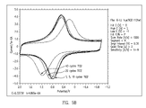
- FIGS. 4A and 4B depict current and potential curves illustrating the performance of a molecular memory device according to one embodiment of the present invention
- FIGS. 5A and 5B illustrate another current and potential curve illustrating the performance of a molecular memory device according to another embodiment of the present invention.
- FIGS. 6A and 6B show impedance-frequency response curves ( FIG. 6A ) for devices according to different embodiments of the present invention and compared to a device without the wetting layer of the present invention, formed according to various process conditions ( FIG. 6B ).
- the invention generally encompasses methods of forming thin films for use in molecular based devices, and devices formed.
- methods of forming thin films molecular based devices, and devices formed therefrom are provided. Some embodiments relate to molecular memory cells, molecular memory arrays, electronic devices including molecular memory, and processing systems and methods for producing molecular memories. Embodiments of the present invention encompass methods and molecular based devices comprising a wetting layer formed therein.
- acyl refers to an organic acid group in which the OH of the carboxyl group is replaced by some other substituent (RCO—), such as described herein as “R” substitutent groups. Examples include, but are not limited to, halo, acetyl and benzoyl.
- alkoxy group means an —O— alkyl group, wherein alkyl is as defined herein.
- An alkoxy group can be unsubstituted or substituted with one or two suitable substituents.
- the alkyl chain of an alkoxy group is from 1 to 6 carbon atoms in length, referred to herein, for example, as “(C1-C6)alkoxy.”
- alkyl by itself or as part of another substituent, refers to a saturated or unsaturated, branched, straight-chain or cyclic monovalent hydrocarbon radical derived by the removal of one hydrogen atom from a single carbon atom of a parent alkane, alkene or alkyne. Also included within the definition of an alkyl group are cycloalkyl groups such as C5 and C6 rings, and heterocyclic rings with nitrogen, oxygen, sulfur or phosphorus (heterocycloalkyl). Alkyl also includes heteroalkyl, with heteroatoms of sulfur, oxygen, nitrogen, and silicon finding particular use in certain embodiments. Alkyl groups can be optionally substituted with R groups, independently selected at each position as described below.
- alkyl groups include, but are not limited to, (C1-C6) alkyl groups, such as methyl, ethyl, propyl, isopropyl, 2-methyl-1-propyl, 2-methyl-2-propyl, 2-methyl-1-butyl, 3-methyl-1-butyl, 2-methyl-3-butyl, 2,2-dimethyl-1-propyl, 2-methyl-1-pentyl, 3-methyl-1-pentyl, 4-methyl-1-pentyl, 2-methyl-2-pentyl, 3-methyl-2-pentyl, 4-methyl-2-pentyl, 2,2-dimethyl-1-butyl, 3,3-dimethyl-1-butyl, 2-ethyl-1-butyl, butyl, isobutyl, t-butyl, pentyl, isopentyl, neopentyl, and hexyl, and longer alkyl groups, such as heptyl, and octyl.
- alkyl is specifically intended to include groups having any degree or level of saturation, i.e., groups having exclusively carbon-carbon single bonds, groups having one or more carbon-carbon double bonds, groups having one or more carbon-carbon triple bonds and groups having mixtures of single, double and triple carbon-carbon bonds. Where a specific level of saturation is intended, the expressions “alkanyl,” “alkenyl,” and “alkynyl” are used.
- Alkanyl by itself or as part of another substituent, refers to a saturated branched, straight-chain or cyclic alkyl radical derived by the removal of one hydrogen atom from a single carbon atom of a parent alkane. “Heteroalkanyl” is included as described above.
- Alkenyl by itself or as part of another substituent, refers to an unsaturated branched, straight-chain or cyclic alkyl radical having at least one carbon-carbon double bond derived by the removal of one hydrogen atom from a single carbon atom of a parent alkene.
- the group may be in either the cis or trans conformation about the double bond(s).
- Suitable alkenyl groups include, but are not limited to (C2-C6) alkenyl groups, such as vinyl, allyl, butenyl, pentenyl, hexenyl, butadienyl, pentadienyl, hexadienyl, 2-ethylhexenyl, 2-propyl-2-butenyl, 4-(2-methyl-3-butene)-pentenyl.
- An alkenyl group can be unsubstituted or substituted with one or more independently selected R groups.
- Alkynyl by itself or as part of another substituent, refers to an unsaturated branched, straight-chain or cyclic alkyl radical having at least one carbon-carbon triple bond derived by the removal of one hydrogen atom from a single carbon atom of a parent alkyne.
- alkyl also included within the definition of “alkyl” is “substituted alkyl”. “Substituted” is usually designated herein as “R”, and refers to a group in which one or more hydrogen atoms are independently replaced with the same or different substituent(s).
- R substituents can be independently selected from, but are not limited to, hydrogen, halogen, alkyl (including substituted alkyl (alkylthio, alkylamino, alkoxy, etc.), cycloalkyl, substituted cycloalkyl, cycloheteroalkyl, and substituted cycloheteroalkyl), aryl (including substituted aryl, heteroaryl or substituted heteroaryl), carbonyl, alcohol, amino, amido, nitro, ethers, esters, aldehydes, sulfonyl, sulfoxyl, carbamoyl, acyl, cyano, thiocyanato, silicon moieties, halogens, sulfur containing moieties, phosphorus containing moieties, etc.
- R substituents include redox active moieties (ReAMs).
- ReAMs redox active moieties
- R and R′ together with the atoms to which they are bonded form a cycloalkyl (including cycloheteroalkyl) and/or cycloaryl (including cycloheteroaryl), which can also be further substituted as desired.
- R is hydrogen when the position is unsubstituted. It should be noted that some positions may allow two or three substitution groups, R and R′, in which case the R and R′ groups may be either the same or different.
- the R groups are used to adjust the redox potential(s) of the subject compound.
- an R group such as a redox active subunit can be added to a macrocycle, particularly a porphyrinic macrocycle to alter its redox potential.
- Certain preferred substituents include, but are not limited to, 4-chlorophenyl, 3-acetamidophenyl, 2,4-dichloro-4-trifluoromethyl, and ferrocene (including ferrocene derivatives).
- preferred substituents provide a redox potential range of less than about 5 volts, preferably less than about 2 volts, more preferably less than about 1 volt.
- the R groups are as defined and depicted in the figures and the text from U.S. Pat. Ser. No. 60/687,464 which is incorporated herein by reference.
- a number of suitable proligands and complexes, as well as suitable substituents, are outlined in U.S. Pat. Nos. 6,212,093; 6,728,129; 6,451,942; 6,777,516; 6,381,169; 6,208,553; 6,657,884; 6,272,038; 6,484,394; and U.S. Pat. No. 7,348,206; Ser. No. 10/682,868; U.S. Pat. No. 7,005,237; Ser. No. 10/834,630; U.S. Pat. Nos.
- aryl or grammatical equivalents herein is meant an aromatic monocyclic or polycyclic hydrocarbon moiety generally containing 5 to 14 carbon atoms (although larger polycyclic rings structures may be made) and any carbocyclic ketone or thioketone derivative thereof, wherein the carbon atom with the free valence is a member of an aromatic ring.
- Aromatic groups include arylene groups and aromatic groups with more than two atoms removed. For the purposes of this application aryl includes heteroaryl.
- Heteroaryl means an aromatic group wherein 1 to 5 of the indicated carbon atoms are replaced by a heteroatom chosen from nitrogen, oxygen, sulfur, phosphorus, boron and silicon wherein the atom with the free valence is a member of an aromatic ring, and any heterocyclic ketone and thioketone derivative thereof.
- heterocycle includes both single ring and multiple ring systems, e.g. thienyl, furyl, pyrrolyl, pyrimidinyl, indolyl, purinyl, quinolyl, isoquinolyl, thiazolyl, naphthalene, phenanthroline, etc.
- aryl is substituted aryl, with one or more substitution groups “R” as defined herein and outlined above and herein.
- substitution groups “R” as defined herein and outlined above and herein.
- perfluoroaryl is included and refers to an aryl group where every hydrogen atom is replaced with a fluorine atom. Also included is oxalyl.
- halogen refers to one of the electronegative elements of group VITA of the periodic table (fluorine, chlorine, bromine, iodine, astatine).
- nitro refers to the NO.sub.2 group.
- amino groups or grammatical equivalents herein is meant —NH2, —NHR and —NRR′ groups, with R and R′ independently being as defined herein.
- pyridyl refers to an aryl group where one CH unit is replaced with a nitrogen atom.
- cyano refers to the —CN group.
- thiocyanato refers to the —SCN group.
- sulfoxyl refers to a group of composition RS(O)— where R is some substitution group as defined herein, including alkyl, (cycloalkyl, perfluoroalkyl, etc.), or aryl (e.g., perfluoroaryl group). Examples include, but are not limited to methylsulfoxyl, phenylsulfoxyl, etc.
- sulfonyl refers to a group of composition RSO2- where R is a substituent group, as defined herein, with alkyl, aryl, (including cycloalkyl, perfluoroalkyl, or perfluoroaryl groups). Examples include, but are not limited to methylsulfonyl, phenylsulfonyl, p-toluenesulfonyl, etc.
- carbamoyl refers to the group of composition R(R′)NC(O)— where R and R′ are as defined herein, examples include, but are not limited to N-ethylcarbamoyl, N,N-dimethylcarbamoyl, etc.
- amido refers to the group of composition R.sup.1CON(R.sup.2)- where R.sup.1 and R.sup.2 are substituents as defined herein. Examples include, but are not limited to acetamido, N-ethylbenzamido, etc.
- acyl refers to an organic acid group in which the OH of the carboxyl group is replaced by some other substituent (RCO—). Examples include, but are not limited to acetyl, benzoyl, etc.
- n is an integer
- the term “amperometric device” is a device capable of measuring the current produced in an electrochemical cell as a result of the application of a specific field potential (“voltage”).
- aryloxy group means an —O— aryl group, wherein aryl is as defined herein.
- An aryloxy group can be unsubstituted or substituted with one or two suitable substituents.
- the aryl ring of an aryloxy group is a monocyclic ring, wherein the ring comprises 6 carbon atoms, referred to herein as “(C6)aryloxy.”
- benzyl means —CH2-phenyl.
- carbonyl is a divalent group of the formula —C(O)—.
- the term “coulometric device” is a device capable of measuring the net charge produced during the application of a potential field (“voltage”) to an electrochemical cell.
- cyano refers to the —CN group.
- the term “different and distinguishable” when referring to two or more oxidation states means that the net charge on the entity (atom, molecule, aggregate, subunit, etc.) can exist in two different states.
- the states are said to be “distinguishable” when the difference between the states is greater than thermal energy at room temperature (e.g., 0° C. to about 40° C.).
- E 1/2 refers to the practical definition of the formal potential (B o ) of a redox process as defined by B ⁇ B o +(RT/nF)ln(D ox /D red ) where R is the gas constant, T is temperature in K (Kelvin), n is the number of electrons involved in the process, F is the Faraday constant (96,485 Coulomb/mole), D ox is the diffusion coefficient of the oxidized species and D red is the diffusion coefficient of the reduced species.
- the term “electrically coupled” when used with reference to a storage molecule and/or storage medium and electrode refers to an association between that storage medium or molecule and the electrode such that electrons move from the storage medium/molecule to the electrode or from the electrode to the storage medium/molecule and thereby alter the oxidation state of the storage medium/molecule.
- Electrical coupling can include direct covalent linkage between the storage medium/molecule and the electrode, indirect covalent coupling (e.g. via a linker), direct or indirect ionic bonding between the storage medium/molecule and the electrode, or other bonding (e.g. hydrophobic bonding).
- no actual bonding may be required and the storage medium/molecule may simply be contacted with the electrode surface. There also need not necessarily be any contact between the electrode and the storage medium/molecule where the electrode is sufficiently close to the storage medium/molecule to permit electron tunneling between the medium/molecule and the electrode.
- the term “electrochemical cell” consists minimally of a reference electrode, a working electrode, a redox-active medium (e.g. a storage medium), and, if necessary, some means (e.g., a dielectric) for providing ionic conductivity between the electrodes and/or between the electrodes and the medium.
- a redox-active medium e.g. a storage medium
- some means e.g., a dielectric
- the dielectric is a component of the storage medium.
- electrode refers to any medium capable of transporting charge (e.g., electrons) to and/or from a storage molecule.
- Preferred electrodes are metals or conductive organic molecules.
- the electrodes can be manufactured to virtually any 2-dimensional or 3-dimensional shape (e.g., discrete lines, pads, planes, spheres, cylinders, etc.).
- the term “fixed electrode” is intended to reflect the fact that the electrode is essentially stable and unmovable with respect to the storage medium. That is, the electrode and storage medium are arranged in an essentially fixed geometric relationship with each other. It is of course recognized that the relationship alters somewhat due to expansion and contraction of the medium with thermal changes or due to changes in conformation of the molecules comprising the electrode and/or the storage medium. Nevertheless, the overall spatial arrangement remains essentially invariant. In a preferred embodiment this term is intended to exclude systems in which the electrode is a movable “probe” (e.g., a writing or recording “head,” an atomic force microscope (AFM) tip, a scanning tunneling microscope (STM) tip, etc.).
- a movable “probe” e.g., a writing or recording “head,” an atomic force microscope (AFM) tip, a scanning tunneling microscope (STM) tip, etc.
- linker is a molecule used to couple two different molecules, two subunits of a molecule, or a molecule to a substrate.
- a metal is designated by “M” or “M n ,” where n is an integer, it is recognized that the metal may be associated with a counter ion.
- R substituents, generally depicted herein as “R.”
- Suitable R groups include, but are not limited to, hydrogen, alkyl, alcohol, aryl, amino, amido, nitro, ethers, esters, aldehydes, sulfonyl, silicon moieties, halogens, cyano, acyl, sulfur containing moieties, phosphorus containing moieties, amido, imido, carbamoyl, linkers, attachment moieties, ReAMs and other subunits. It should be noted that some positions may allow two substitution groups, R and R′, in which case the R and R′ groups may be either the same or different, and it is generally preferred that one of the substitution groups be hydrogen.
- the R groups are as defined and depicted in the figures and the text from a number of suitable proligands and complexes, as well as suitable substituents, as outlined in U.S. Pat. Nos. 6,212,093; 6,728,129; 6,451,942; 6,777,516; 6,381,169; 6,208,553; 6,657,884; 6,272,038; 6,484,394; and U.S. Pat. No. 7,348,206; Ser. No. 10/682,868; U.S. Pat. No. 7,005,237; Ser. No. 10/834,630; U.S. Pat. Nos.
- sulfoxyl refers to a group of composition RS(O)— where R is some alkyl, aryl, cycloalkyl, perfluoroalkyl, or perfluoroaryl group. Examples include, but are not limited to methylsulfoxyl, phenylsulfoxyl, etc.
- sulfonyl refers to a group of composition RSO 2 , where R is some alkyl, aryl, cycloalkyl, perfluoroalkyl, or perfluoroaryl group. Examples include, but are not limited to methylsulfonyl, phenylsulfonyl, p-toluenesulfonyl, etc.
- subunit refers to a redox-active component of a molecule.
- thiocyanato refers to the —SCN group.
- FIGS. 1A-1D an exemplary embodiment of a molecular based device 10 of the present invention is shown as generally comprised of substrate 12 , wetting layer 14 atop the substrate 12 , molecular layer 16 atop the wetting layer 14 , and charge transfer layer 18 atop the molecular layer 16 .
- the substrate 12 may be comprised of any desired material, such as glass, plastic, silicon, GaAs, and the like.
- the substrate 12 is comprised of a silicon wafer having conductive and non-conductive regions or surfaces.
- the conductive surfaces may be comprised of conductive materials such as but not limited to titanium, aluminum, copper, tungsten, TiN, TaN, and the like.
- the non-conductive surfaces may be comprised of dielectric materials such as but not limited to SiO 2 , Al 2 O 3 , HfO 2 , and the like.
- the substrate 12 typically, but not necessarily, comprises patterned structures formed therein.
- the wetting layer 14 is disposed between the substrate 12 and the molecular layer 16 . In some embodiments the wetting layer 14 is disposed directly between the substrate 12 and the molecular layer 16 . In other embodiments, the wetting layer is not directly disposed between the substrate and molecular layers, and instead one or more other layers, such as a barrier layer, may be formed in between.
- the wetting layer 14 promotes improved nucleation of the molecular layer 16 . Additionally in some embodiments, the wetting layer 14 can equalize the surface tension across substrate 12 , thus enhancing the wetting properties during subsequent deposition of the charge transfer layer 18 .
- the wetting layer 14 may be comprised broadly of any material that enhances or promotes the wetting and/or the nucleation of layers formed atop of, or subsequent to, the molecular layer 16 , such as the charge transfer layer 18 .
- the wetting layer 14 may be comprised broadly of any material that enhances the performance of the molecular based device, such as the molecular charge and/or speed.
- Suitable materials for the wetting layer 14 include but are not limited to: titanium oxides, ruthenium oxides, tantalum oxides, aluminum oxides, hafnium oxide, or inorganic nitrides. In one preferred embodiment, the wetting layer 14 is comprised of TiO 2 .
- Molecular based devices of the present invention employ molecular layer 16 , formed atop wetting layer 14 .
- the molecular layer 16 is comprised of redox active molecules (ReAM).
- Redox active molecules suitable for use in the present invention are described in detail below.
- the molecular layer 16 is comprised of redox active molecules that include functional groups configured to promote and/or enhance the wetting behavior of the charge transfer layer 18 .
- the wetting layer 14 may still be present.
- the wetting layer 14 may be omitted, since the functional groups of the redox active molecules provide the wetting function.
- the charge transfer layer 18 may be comprised of any suitable material.
- the charge transfer layer 18 is comprised of an electrolyte.
- the charge transfer layer 18 is comprised of a phosphonium based electrolyte, such as that described in detail in U.S. patent application Ser. No. 12/027,924; and U.S. Provisional Patent application Ser. No. 61/080,650, the disclosures of both of which are hereby incorporated by reference in their entirety.
- the charge transfer layer 18 is comprised of PHL21-TCM.
- FIG. 2A to 2D are micrographs showing improved wetting for devices formed with a wetting layer of TiO 2 formed below the molecular layer, verses devices formed with no wetting layer below the molecular layer.
- devices formed according to embodiments of the present invention exhibit significantly improved wetting to form substantially uniform films and devices. This improvement is realized at both the post charge transfer layer deposition stage, as well as after counter electrode metallization processing.
- a multiple or multi-layered molecular based device 20 is provided.
- one or more of the wetting layer 14 and/or molecular layer 16 are repeated atop the substrate as illustrated in FIG. 3 .
- multiple wetting layers 14 and multiple molecular layers 16 can be formed and layered repeatedly any desired number of times to achieve a desired property.
- desired properties include but are not limited to: desired charge, tuning the wetting behavior of the subsequent charge transfer layer 18 , speed of the device, and the like.
- the molecular based devices of the present invention may be formed by a variety of methods. Referring again to FIGS. 1A to 1D , an exemplary embodiment of the method is shown in sequential steps.
- the substrate 12 is provided.
- the substrate includes conductive 12 a and non-conductive 12 b surfaces or regions.
- a thin wetting layer 14 is formed or deposited atop the substantial to entire surface of the substrate 12 .
- the wetting layer 14 is comprised of TiO 2 .
- the wetting layer 14 may comprised of any desired thickness. In some embodiments, the thickness of the wetting layer 14 is in the range of about 0.1 to 5.0 nm.
- molecular layer 16 is formed or deposited atop the wetting layer 14 as shown in FIG. 1C .
- the molecular layer 16 is comprised of active redox molecules.
- the molecular layer 16 may comprised of any desired thickness. In some embodiments, the thickness of the molecular layer 16 is in the range of about 0.1 to 10.0 nm.
- the charge transfer layer 18 is formed or deposited atop the molecular layer 16 as illustrated in FIG. 1D .
- the charge transfer layer 18 is comprised of an electrolyte, such as but not limited to a phosphonium based electrolyte.
- the thickness of the charge transfer layer 18 is in the range of about 2.0 to 100.0 nm.
- Deposition of the layers may be accomplished by any suitable deposition method, such as by chemical vapor deposition (CVD), plasma enhanced CVD, atomic layer deposition (ALD), sputtering and the like.
- CVD chemical vapor deposition
- ALD atomic layer deposition
- the wetting 14 and molecular 16 layers are deposited by ALD techniques as described below.
- Atomic layer deposition is generally carried out by sequential steps or “pulses” where a reactant precursor in gaseous or vapor form is injected into a process chamber and adsorbs on the surface of a substrate.
- the process chamber is then purged either by evacuation, inert gas purge, or both.
- a separate pulse of another reactant precursor is conveyed to the process chamber and reacts with the adsorbed first precursor to form a monolayer of desired material on the surface of the substrate.
- the process chamber is then purged again, and this completes one ALD cycle. The cycle is then repeated until a layer of desired thickness is formed.
- ALD differs from traditional CVD in that the precursors are conveyed separately and sequentially, as opposed to the CVD process where the precursors are mixed together in the process chamber and reacted in the proximity of the substrate to deposit a layer on the substrate.
- the wetting layer 14 is formed atop the substrate 12 by ALD. It should be understood that other deposition techniques may be used, and fall within the scope of the present invention, such as thermal vapor transfer (sublimation), CVD, physical vapor deposition (PVD), or any other deposition technique capable of depositing a substantially uniform film of desired thickness.
- ALD atomic layer deposition
- the substrate 12 is placed in a deposition chamber and heated to a temperature in the range of 85° C. to 400° C. Any suitable ALD deposition chamber may be used.
- H 2 O vapor is adsorbed to the surface by injecting or flowing a metered pulse over the surface of the substrate.
- the H 2 O vapor is flowed in an inert carrier gas at a flowrate in the range of 1 to 50 sccm, for a period of time in the range of 1 ⁇ 10 ⁇ 5 to 10 seconds.
- This first step is carried out at a process pressure in the range of 1 ⁇ 10 ⁇ 5 to 1.0 Torr.
- the H 2 O vapor is then purged from the deposition chamber.
- Other precursors such as methanol, ethanol, isopropanol, and the like can be used.
- a volatile titanium containing precursor is injected into the deposition chamber in another metered pulse and subsequently reacts with the adsorbed water to form a single layer of TiO 2 on the surface of the substrate.
- Any suitable titanium containing precursor may be used, such as but not limited to: tetrakis (dimethylamido) titanium (IV), Bis(diethylamino) bis(diisopropylamino) titanium(IV), Tetrakis(diethylamido) titanium(IV), Titanium(IV) chloride, Tetrakis(ethylmethylamido) titanium(IV) or similar.
- the titanium containing precursor is injected in an inert carrier gas at a flowrate in the range of 1 to 50 sccm, for a period of time in the range of 1 ⁇ 10 ⁇ 5 to 10 seconds.
- This second step is carried out at a process pressure in the range of 1 ⁇ 10 ⁇ 5 to 1.0 Torr.
- the titanium continuing precursor is then purged from the deposition chamber. This completes one ALD cycle.
- the process is then repeated in a cyclic manner until the desired thickness of the wetting layer is achieved.
- the thickness of the wetting layer can be controlled at the sub-nanometer level and can be tuned to achieve the desired performance criteria.
- the substrate 12 is now covered with a thin, substantially uniform wetting layer 14 onto which the molecular layer 16 and subsequent charge transfer layer 18 are deposited.
- the wetting layer 14 is comprised of ruthenium or tantalum oxide.
- a ruthenium or tantalum containing precursor as the case may be, is injected into the deposition chamber in a metered pulse.
- suitable ruthenium and tantalum precursors include, but are not limited to: Bis(ethylcyclopentadienyl) ruthenium(II), Pentakis(dimethylamido)tantalum(V), Tris(diethylamido)(tert-butylimido) tantalum(V), and the like.
- This invention addresses prior issues by depositing a very thin wetting layer, such as TiO 2 film, preferably of 0.1 to 0.5 nm, over the entire substrate prior to deposition of the redox molecule.
- a very thin wetting layer such as TiO 2 film
- Our application utilized atomic layer deposition (ALD) processes for both TiO 2 and redox molecules at temperatures ranging from 85° C. to 400° C.
- ALD atomic layer deposition
- the TiO 2 equalizes the surface tension across the entire substrate enhancing the wetting properties during deposition of the subsequent charge transfer layer. This results in significant improvement in uniformity and device performance (i.e. molecular charge and speed).
- Our application utilizes a charge transfer layer comprised of phosphonium based electrolytes, however, tuning the surface tension of the underlying substrate would have similar benefits for deposition of any subsequent materials.
- an upper conductive material can be applied to complete the device (in the illustrative embodiment a capacitive storage cell), utilizing ALD, CVD, PVD or thermal evaporation.
- the molecular based devices of the present invention described herein can be employed to synthesize a wide range of hybrid components and/or devices, such as for example memory devices and elements.
- devices formed herein are used to form molecular storage or memory devices having molecular layer 16 where information is stored in a redox-active information storage molecule.
- Redox-active molecule herein is meant to refer to a molecule or component of a molecule that is capable of being oxidized or reduced, e.g., by the application of a suitable voltage.
- ReAMs can include, but are not limited to macrocycles including porphyrin and porphyrin derivatives, ferrocene and ferrocene derivatives, as well as non-macrocyclic compounds, and includes sandwich compounds, e.g. as described herein.
- ReAMs can comprise multiple subunits, for example, in the case of dyads or triads.
- ReAMs useful in the present invention, all based on polydentate proligands, including macrocyclic and non-macrocyclic moieties.
- Suitable proligands fall into two categories: ligands which use nitrogen, oxygen, sulfur, carbon or phosphorus atoms (depending on the metal ion) as the coordination atoms (generally referred to in the literature as sigma ( ⁇ ) donors) and organometallic ligands such as metallocene ligands (generally referred to in the literature as pi ( ⁇ ) donors, and depicted herein as Lm).
- a single ReAM may have two or more redox active.
- FIG. 13A of U.S. Publication No. 2007/0108438 shows two redox active subunits, a porphorin (shown in the absence of a metal), and ferrocense.
- sandwich coordination compounds are considered a single ReAM. This is to be distinguished from the case where these ReAMs are polymerized as monomers.
- the metal ions/complexes of the invention may be associated with a counterion, not generally depicted herein.
- the ReAM is a macrocyclic ligand, which includes both macrocyclic proligands and macrocyclic complexes.
- macrocyclic proligand herein is meant a cyclic compound which contain donor atoms (sometimes referred to herein as “coordination atoms”) oriented so that they can bind to a metal ion and which are large enough to encircle the metal atom.
- the donor atoms are heteroatoms including, but not limited to, nitrogen, oxygen and sulfur, with the former being especially preferred.
- different metal ions bind preferentially to different heteroatoms, and thus the heteroatoms used can depend on the desired metal ion.
- a single macrocycle can contain heteroatoms of different types.
- a “macrocyclic complex” is a macrocyclic proligand with at least one metal ion; in some embodiments the macrocyclic complex comprises a single metal ion, although as described below, polynucleate complexes, including polynucleate macrocyclic complexes, are also contemplated.
- macrocyclic ligands find use in the present invention, including those that are electronically conjugated and those that may not be; however, the macrocyclic ligands of the invention preferably have at least one, and preferably two or more oxidation states, with 4, 6 and 8 oxidation states being of particular significance.
- FIGS. 11 and 14 A broad schematic of suitable macrocyclic ligands are shown and described in FIGS. 11 and 14 of U.S. Publication No. 2007/0108438, all of which is incorporated by reference herein in addition to FIGS. 11 and 14.
- a 16 member ring when the —X— moiety contains a single atom, either carbon or a heteroatom
- 17 membered rings where one of the —X— moieties contains two skeletal atoms
- 18 membered rings where two of the —X— moieties contains two skeletal atoms
- 19 membered rings where three of the —X— moieties contains two skeletal atoms
- 20 membered rings where all four of the —X— moieties contains two skeletal atoms
- Each —X— group is independently selected.
- the -Q- moiety, together with the skeletal —C— heteroatom —C (with either single or double bonds independently connecting the carbons and heteroatom) for 5 or 6 membered rings that are optionally substituted with 1 or 2 (in the case of 5 membered rings) or 1, 2, or 3 (in the case of 6 membered rings) with independently selected R2 groups.
- the rings, bonds and substitutents are chosen to result in the compound being electronically conjugated, and at a minimum to have at least two oxidation states.
- the macrocyclic ligands of the invention are selected from the group consisting of porphyrins (particularly porphyrin derivatives as defined below), and cyclen derivatives.
- porphyrins including porphyrin derivatives.
- Such derivatives include porphyrins with extra rings ortho-fused, or ortho-perfused, to the porphyrin nucleus, porphyrins having a replacement of one or more carbon atoms of the porphyrin ring by an atom of another element (skeletal replacement), derivatives having a replacement of a nitrogen atom of the porphyrin ring by an atom of another element (skeletal replacement of nitrogen), derivatives having substituents other than hydrogen located at the peripheral (meso-, (3- or core atoms of the porphyrin, derivatives with saturation of one or more bonds of the porphyrin (hydroporphyrins, e.g., chlorins, bacteriochlorins, isobacteriochlorins, decahydroporphyrins, corphins, pyrrocorphins, etc.), derivatives having one or more atoms, including pyrrolic
- porphyrin derivatives include, but are not limited to the chlorophyll group, including etiophyllin, pyrroporphyrin, rhodoporphyrin, phylloporphyrin, phylloerythrin, chlorophyll a and b, as well as the hemoglobin group, including deuteroporphyrin, deuterohemin, hemin, hematin, protoporphyrin, mesohemin, hematoporphyrin mesoporphyrin, coproporphyrin, uruporphyrin and turacin, and the series of tetraarylazadipyrromethines.
- each unsaturated position can include one or more substitution groups as defined herein, depending on the desired valency of the system.
- the redox-active molecule may be a metallocene, which can be substituted at any appropriate position, using R groups independently selected herein.
- a metallocene which finds particular use in the invention includes ferrocene and its derivatives.
- preferred substituents include, but are not limited to, 4-chlorophenyl, 3-acetamidophenyl, 2,4-dichloro-4-trifluoromethyl. Preferred substituents provide a redox potential range of less than about 2 volts.
- oxidation potentials of the members of the series can be routinely altered by changing the metal (M) or the substituents.
- FIG. 12H of U.S. Publication No. 2007/0108438 Another example of a redox-active molecule comprised of a porphyrin is shown in FIG. 12H of U.S. Publication No. 2007/0108438 where F is a redox-active subunit (such as ferrocense, a substituted ferrocene, a metalloporphyrin, or a metallochlorin, and the like), J1 is a linker, M is a metal (such as Zn, Mg, Cd, Hg, Cu, Ag, Au, Ni, Pd, Pt, Co, Rh, Ir, Mn, B, Al, Ga, Pb and Sn) S1 and S2 are independently selected from the group of aryl, phenyl, cyclalkyl, alkyl, halogen, alkoxy, alkylhio, perfluoroalkyl, perfluoroaryl, pyridyl, cyano, thiocyana
- Control over the hole-storage and hole-hopping properties of the redox-active units of the redox-active molecules used in the memory devices of the present invention allows fine control over the architecture of the memory device.
- the hole-storage properties depend on the oxidation potential of the redox-active units or subunits that are themselves or are that are used to assemble the storage media used in the devices of this invention.
- the hole-storage properties and redox potential can be tuned with precision by choice of base molecule(s), associated metals and peripheral substituents (Yang et al. (1999) J. Porphyrins Phthalocyanines, 3: 117-147), the disclosure of which is herein incorporated by this reference.
- Mg porphyrins are more easily oxidized than Zn porphyrins, and electron withdrawing or electron releasing aryl groups can modulate the oxidation properties in predictable ways.
- Hole-hopping occurs among isoenergetic porphyrins in a nanostructure and is mediated via the covalent linker joining the porphyrins (Seth et al. (1994) J. Am. Chem. Soc., 116: 10578-10592, Seth et al (1996) J. Am. Chem. Soc., 118: 11194-11207, Strachan et al. (1997) J. Am. Chem. Soc., 119: 11191-11201; Li et al.
- the oxidation potential is predicted by comparison of the experimentally determined oxidation potential of a base molecule and that of a base molecule bearing one substituent in order to determine the shift in potential due to that particular substituent. The sum of such substituent-dependent potential shifts for the respective substituents then gives the predicted oxidation potential.
- redox-active molecules for use in the methods of this invention can readily be determined.
- the molecule(s) of interest are simply polymerized and coupled to a surface (e.g., a hydrogen passivated surface) according to the methods of this invention.
- sinusoidal voltammetry can be performed (e.g., as described herein or in U.S. Pat. Nos. 6,272,038; 6,212,093; and 6,208,553, PCT Publication WO 01/03126, or by (Roth et al. (2000) Vac. Sci. Technol. B 18:2359-2364; Roth et al. (2003) J. Am. Chem. Soc.
- porphyrin included within the definition of “porphyrin” are porphyrin complexes, which comprise the porphyrin proligand and at least one metal ion. Suitable metals for the porphyrin compounds will depend on the heteroatoms used as coordination atoms, but in general are selected from transition metal ions.
- transition metals typically refers to the 38 elements in groups 3 through 12 of the periodic table. Typically transition metals are characterized by the fact that their valence electrons, or the electrons they use to combine with other elements, are present in more than one shell and consequently often exhibit several common oxidation states.
- the transition metals of this invention include, but are not limited to one or more of scandium, titanium, vanadium, chromium, manganese, iron, cobalt, nickel, copper, zinc, yttrium, zirconium, niobium, molybdenum, technetium, ruthenium, rhodium, palladium, silver, cadmium, hafnium, tantalum, tungsten, rhenium, osmium, iridium, platinum, gold, mercury, rutherfordium, and/or oxides, and/or nitrides, and/or alloys, and/or mixtures thereof.
- FIGS. 17 and 13C of U.S. Publication No. 2007/0108438 shows a number of macrocyclic proligands loosely based on cyclen/cyclam derivatives, which can include skeletal expansion by the inclusion of independently selected carbons or heteroatoms.
- at least one R group is a redox active subunit, preferably electronically conjugated to the metal.
- two or more neighboring R2 groups form cycle or an aryl group.
- macrocyclic complexes relying organometallic ligands are used.
- transition metal organometallic compounds with ⁇ -bonded organic ligands see Advanced Inorganic Chemistry, 5th Ed., Cotton & Wilkinson, John Wiley & Sons, 1988, chapter 26; Organometallics, A Concise Introduction, Elschenbroich et al., 2nd Ed., 1992, VCH; and Comprehensive Organometallic Chemistry II, A Review of the Literature 1982-1994, Abel et al.
- organometallic ligands include cyclic aromatic compounds such as the cyclopentadienide ion [C5H5( ⁇ 1)] and various ring substituted and ring fused derivatives, such as the indenylide ( ⁇ 1) ion, that yield a class of bis(cyclopentadieyl)metal compounds, (i.e. the metallocenes); see for example Robins et al., J. Am. Chem. Soc. 104:1882-1893 (1982); and Gassman et al., J. Am. Chem. Soc.
- ferrocene [(C5H5)2Fe] and its derivatives are prototypical examples which have been used in a wide variety of chemical (Connelly et al., Chem. Rev. 96:877-910 (1996), incorporated by reference) and electrochemical (Geiger et al., Advances in Organometallic Chemistry 23:1-93; and Geiger et al., Advances in Organometallic Chemistry 24:87, incorporated by reference) electron transfer or “redox” reactions.
- Metallocene derivatives of a variety of the first, second and third row transition metals are useful as redox moieties (and redox subunits).
- organometallic ligands include cyclic arenes such as benzene, to yield bis(arene)metal compounds and their ring substituted and ring fused derivatives, of which bis(benzene)chromium is a prototypical example.
- Other acyclic ⁇ -bonded ligands such as the allyl( ⁇ 1) ion, or butadiene yield potentially suitable organometallic compounds, and all such ligands, in conjunction with other ⁇ -bonded and ⁇ -bonded ligands constitute the general class of organometallic compounds in which there is a metal to carbon bond. Electrochemical studies of various dimers and oligomers of such compounds with bridging organic ligands, and additional non-bridging ligands, as well as with and without metal-metal bonds are all useful.
- the ligand is generally attached via one of the carbon atoms of the organometallic ligand, although attachment may be via other atoms for heterocyclic ligands.
- Preferred organometallic ligands include metallocene ligands, including substituted derivatives and the metalloceneophanes (see page 1174 of Cotton and Wilkenson, supra).
- derivatives of metallocene ligands such as methylcyclopentadienyl, with multiple methyl groups being preferred, such as pentamethylcyclopentadienyl, can be used to increase the stability of the metallocene.
- the metallocene is derivatized with one or more substituents as outlined herein, particularly to alter the redox potential of the subunit or moiety.
- any combination of ligands may be used.
- Preferred combinations include: a) all ligands are nitrogen donating ligands; b) all ligands are organometallic ligands.
- the ReAMs are sandwich coordination complexes.
- the terms “sandwich coordination compound” or “sandwich coordination complex” refer to a compound of the formula L-Mn-L, where each L is a heterocyclic ligand (as described below), each M is a metal, n is 2 or more, most preferably 2 or 3, and each metal is positioned between a pair of ligands and bonded to one or more hetero atom (and typically a plurality of hetero atoms, e.g., 2, 3, 4, 5) in each ligand (depending upon the oxidation state of the metal).
- sandwich coordination compounds are not organometallic compounds such as ferrocene, in which the metal is bonded to carbon atoms.
- the ligands in the sandwich coordination compound are generally arranged in a stacked orientation (i.e., are generally cofacially oriented and axially aligned with one another, although they may or may not be rotated about that axis with respect to one another) (see, e.g., Ng and Jiang (1997) Chemical Society Reviews 26: 433-442) incorporated by reference.
- Sandwich coordination complexes include, but are not limited to “double-decker sandwich coordination compound” and “triple-decker sandwich coordination compounds”. The synthesis and use of sandwich coordination compounds is described in detail in U.S. Pat. Nos. 6,212,093; 6,451,942; 6,777,516; and polymerization of these molecules is described in U.S. Publication No. 2007/0123618, all of which are included herein, particularly the individual substitutent groups that find use in both sandwich complexes and the “single” macrocycle” complexes.
- double-decker sandwich coordination compound refers to a sandwich coordination compound as described above where n is 2, thus having the formula L′-M′-LZ, wherein each of L1 and LZ may be the same or different (see, e.g., Jiang et al. (1999) J. Porphyrins Phthalocyanines 3: 322-328) and U.S. Pat. Nos. 6,212,093; 6,451,942; 6,777,516; and polymerization of these molecules is described in U.S. Publication No. 2007/0123618, hereby incorporated by reference in its entirety.
- triple-decker sandwich coordination compound refers to a sandwich coordination compound as described above where n is 3, thus having the formula L1-M1 LZ-MZ-L3, wherein each of L1, LZ and L3 may be the same or different, and M1 and MZ may be the same or different (see, e.g., Arnold et al. (1999) Chemistry Letters 483-484), and U.S. Pat. Nos. 6,212,093; 6,451,942; 6,777,516; and polymerization of these molecules is described in U.S. Publication No. 2007/0123618, hereby incorporated by reference in their entirety.
- polymers of these sandwich compounds are also of use; this includes “dyads” and “triads” as described in U.S. Pat. Nos. 6,212,093; 6,451,942; 6,777,516; and polymerization of these molecules is described in U.S. Publication No. 2007/0123618, all of which are incorporated by reference.
- ReAMs comprising non-macrocyclic chelators are bound to metal ions to form non-macrocyclic chelate compounds, since the presence of the metal allows for multiple proligands to bind together to give multiple oxidation states.
- nitrogen donating proligands are used. Suitable nitrogen donating proligands are well known in the art and include, but are not limited to, NH2; NHR; NRR′; pyridine; pyrazine; isonicotinamide; imidazole; bipyridine and substituted derivatives of bipyridine; terpyridine and substituted derivatives; phenanthrolines, particularly 1,10-phenanthroline (abbreviated phen) and substituted derivatives of phenanthrolines such as 4,7-dimethylphenanthroline and dipyridol[3,2-a:2′,3′-c]phenazine (abbreviated dppz); dipyridophenazine; 1,4,5,8,9,12-hexaazatriphenylene (abbreviated hat); 9,10-phenanthrenequinone diimine (abbreviated phi); 1,4,5,8-tetraazaphenanthrene (abbreviated tap); 1,4,8,11-tetra
- Substituted derivatives including fused derivatives, may also be used.
- macrocylic ligands that do not coordinatively saturate the metal ion, and which require the addition of another proligand, are considered non-macrocyclic for this purpose.
- Suitable sigma donating ligands using carbon, oxygen, sulfur and phosphorus are known in the art.
- suitable sigma carbon donors are found in Cotton and Wilkenson, Advanced Organic Chemistry, 5th Edition, John Wiley & Sons, 1988, hereby incorporated by reference; see page 38, for example.
- suitable oxygen ligands include crown ethers, water and others known in the art.
- Phosphines and substituted phosphines are also suitable; see page 38 of Cotton and Wilkenson.
- oxygen, sulfur, phosphorus and nitrogen-donating ligands are attached in such a manner as to allow the heteroatoms to serve as coordination atoms.
- polydentate ligands that are polynucleating ligands, e.g. they are capable of binding more than one metal ion. These may be macrocyclic or non-macrocyclic.
- methods of forming redox molecules on a molecular based semiconductor device are provided. More specifically, methods of depositing redox active molecules on a substrate by atomic layer deposition to form a molecular based semiconductor device are provided.
- a method of depositing a molecular layer on a substrate in a deposition chamber comprising the steps of: conveying H 2 O vapor to the deposition chamber to form a monolayer on the surface of the substrate; purging the deposition chamber; and conveying one or more redox-active molecules to the deposition chamber wherein the redox-active molecules react with the monolayer to form a molecular layer on the surface of the substrate.
- the method is carried out at a temperature in the range of 85° C. to 400° C.
- the utilization of H 2 O vapor to form a monolayer of redox-active molecules on the substrate surface is molecule specific and is not required in all cases.
- H 2 O vapor is flowed in an inert carrier gas at a flowrate in the range of 1 to 50 sccm, for a period of time in the range of 1 ⁇ 10 ⁇ 5 to 10 seconds.
- This first step is carried out at a process pressure in the range of 1 ⁇ 10 ⁇ 5 to 1 Torr.
- the H 2 O vapor is then purged from the deposition chamber.
- one or more redox-active molecules are flowed into the deposition chamber in an inert carrier gas at a flowrate in the range of 1 to 50 sccm, for a period of time in the range of 1 ⁇ 10 ⁇ 5 to 10 seconds.
- This second step is carried out at a process pressure in the range of 1 ⁇ 10 ⁇ 5 to 1 Torr.
- the deposition chamber is then purged.
- a pause of 1 to 100 seconds may be preferred between injection of the redox-active molecule and the deposition chamber purge.
- the process can then be repeated in a cyclic manner until the desired property such as thin film thickness, charge, or similar is achieved.
- the term “memory element,” “memory cell,” or “storage cell” refer to an electrochemical cell that can be used for the storage of information.
- Preferred “storage cells” are discrete regions of storage medium addressed by at least one and preferably by two electrodes (e.g., a working electrode and a reference electrode).
- the storage cells can be individually addressed (e.g., a unique electrode is associated with each memory element) or, particularly where the oxidation states of different memory elements are distinguishable, multiple memory elements can be addressed by a single electrode.
- the memory element can optionally include a dielectric (e.g., a dielectric impregnated with counter ions).
- electrode refers to any medium capable of transporting charge (e.g., electrons) to and/or from a storage molecule.
- Preferred electrodes are metals and conductive organic molecules, including, but not limited to, Group III elements (including doped and oxidized Group III elements), Group IV elements (including doped and oxidized Group IV elements), Group V elements (including doped and oxidized Group V elements) and transition metals (including transition metal oxides and transition metal nitrides).
- the electrodes can be manufactured to virtually any 2-dimensional or 3-dimensional shape (e.g., discrete lines, pads, planes, spheres, cylinders).
- the term “multiple oxidation states” means more than one oxidation state.
- the oxidation states may reflect the gain of electrons (reduction) or the loss of electrons (oxidation).
- multiporphyrin array refers to a discrete number of two or more covalently-linked porphyrinic macrocycles.
- the multiporphyrin arrays can be linear, cyclic, or branched.
- output of an integrated circuit refers to a voltage or signal produced by one or more integrated circuit(s) and/or one or more components of an integrated circuit.
- the term “present on a single plane,” when used in reference to a memory device of this invention refers to the fact that the component(s) (e.g. storage medium, electrode(s), etc.) in question are present on the same physical plane in the device (e.g. are present on a single lamina). Components that are on the same plane can typically be fabricated at the same time, e.g., in a single operation. Thus, for example, all of the electrodes on a single plane can typically be applied in a single (e.g., sputtering) step (assuming they are all of the same material).
- a potentiometric device is a device capable of measuring potential across an interface that results from a difference in the equilibrium concentrations of redox molecules in an electrochemical cell.
- the term “oxidation” refers to the loss of one or more electrons in an element, compound, or chemical substituent/subunit.
- an oxidation reaction electrons are lost by atoms of the element(s) involved in the reaction. The charge on these atoms must then become more positive. The electrons are lost from the species undergoing oxidation and so electrons appear as products in an oxidation reaction.
- An oxidation taking place in the reaction Fe 2+ (aq) ⁇ Fe 3+ (aq)+e ⁇ because electrons are lost from the species being oxidized, Fe 2+ (aq), despite the apparent production of electrons as “free” entities in oxidation reactions.
- the term reduction refers to the gain of one or more electrons by an element, compound, or chemical substituent/subunit.
- oxidation state refers to the electrically neutral state or to the state produced by the gain or loss of electrons to an element, compound, or chemical substituent/subunit.
- oxidation state refers to states including the neutral state and any state other than a neutral state caused by the gain or loss of electrons (reduction or oxidation).
- the term “read” or “interrogate” refer to the determination of the oxidation state(s) of one or more molecules (e.g. molecules comprising a storage medium).
- redox-active unit or “redox-active subunit” refers to a molecule or component of a molecule that is capable of being oxidized or reduced by the application of a suitable voltage.
- the term “refresh” when used in reference to a storage molecule or to a storage medium refers to the application of a voltage to the storage molecule or storage medium to re-set the oxidation state of that storage molecule or storage medium to a predetermined state (e.g., the oxidation state the storage molecule or storage medium was in immediately prior to a read).
- reference electrode is used to refer to one or more electrodes that provide a reference (e.g., a particular reference voltage) for measurements recorded from the working electrode.
- a reference e.g., a particular reference voltage
- the reference electrodes in a memory device of this invention are at the same potential although in some embodiments this need not be the case.
- a “sinusoidal voltammeter” is a voltammetric device capable of determining the frequency domain properties of an electrochemical cell.
- the term “storage density” refers to the number of bits per volume and/or bits per molecule that can be stored. When the storage medium is said to have a storage density greater than one bit per molecule, this refers to the fact that a storage medium preferably comprises molecules wherein a single molecule is capable of storing at least one bit of information.
- the term “storage location” refers to a discrete domain or area in which a storage medium is disposed. When addressed with one or more electrodes, the storage location may form a storage cell. However if two storage locations contain the same storage media so that they have essentially the same oxidation states, and both storage locations are commonly addressed, they may form one functional storage cell.
- the term “storage medium” refers to a composition comprising a molecular based device of the invention.
- a substrate is a, preferably solid, material suitable for the attachment of one or more molecules.
- Substrates can be formed of materials including, but not limited to glass, plastic, silicon, minerals (e.g., quartz), semiconducting materials, ceramics, metals, etc.
- the term “voltammetric device” is a device capable of measuring the current produced in an electrochemical cell as a result of the application of a voltage or change in voltage.
- a voltage source is any source (e.g. molecule, device, circuit, etc.) capable of applying a voltage to a target (e.g., an electrode).
- working electrode is used to refer to one or more electrodes that are used to set or read the state of a storage medium and/or storage molecule.
- a molecular storage device comprising a substrate, a wetting layer atop the substrate; a molecular layer atop the wetting layer; and a charge transfer layer atop the molecular layer.
- the invention encompasses a molecular memory element that includes a switching device, a bit line and a word line coupled to the switching device and a molecular storage device accessible through the switching device.
- the molecular storage device is capable of being placed in two or more discrete states, wherein the molecular storage device is placed in one of the discrete states by signals applied to the bit and word line.
- the molecular storage device comprises a substrate, a wetting layer atop the substrate; a molecular layer atop the wetting layer; and a charge transfer layer atop the molecular layer.
- Another embodiment encompasses molecular memory arrays comprising a plurality of molecular storage elements where each molecular storage element is capable of being placed in two or more discrete states.
- a plurality of bit lines and word lines are coupled to the plurality of molecular storage elements such that each molecular storage element is coupled to and addressable by at least one bit line and at least one word line.
- the molecular memory device may include an addressable array of molecular storage elements.
- An address decoder receives a coded address and generates word line signals corresponding to the coded address.
- a word line driver is coupled to the address decoder and produces amplified word line signals.
- the amplified word line signals control switches that selectively couple members of the array of molecular storage elements to bit lines.
- Read/write logic coupled to the bit lines determines whether the molecular memory device is in a read mode or a write mode. In a read mode, sense amplifiers coupled to each bit line detect an electronic state of the selectively coupled molecular storage elements and produce a data signal on the bit line indicative of the electronic state of the selectively coupled molecular storage elements. In a write mode, the read/write logic drives a data signal onto the bit lines and the selectively coupled molecular storage elements.
- Another embodiment encompasses devices including logic integrated with embedded molecular memory devices such as application specific integrated circuit (ASIC) and system on chip (SOC) devices and the like.
- ASIC application specific integrated circuit
- SOC system on chip
- Such implementations comprise one or more functional components formed monolithically with and interconnected to molecular memory devices.
- the functional components may comprise solid state electronic devices and/or molecular electronic devices.
- the molecular storage device is implemented as a stacked structured formed subsequent to and above a semiconductor substrate having active devices formed therein.
- the molecular storage device is implemented as a micron or nanometer sized hole in a semiconductor substrate have active devices formed therein.
- the molecular storage device is fabricated using processing techniques that are compatible with the semiconductor substrate and previously formed active devices in the semiconductor substrate.
- inventions include the use of components independently selected from transistor switching devices including field effect transistor; a row decoder coupled to the word line; a column decoder coupled to the bit line; a current preamplifier connected to the bit line; a sense amplifier connected to the bit line, an address decoder that receives a coded address and generates word line signals corresponding to the coded address, a line driver coupled to the address decoder wherein the line driver produces amplified word line signals (optionally wherein the amplified word line signals control switches that selectively couple members of the array of molecular storage elements to bit lines), read/write logic coupled to the bit lines, wherein the read/write logic determines whether the molecular memory devices is in a read mode or a write mode, sense amplifiers coupled to each bit line, wherein when the device is in a read mode, sense amplifiers coupled to each bit line detect an electronic state of the selectively coupled molecular storage elements and produce a data signal on the bit line indicative of the electronic state of the selectively coupled molecular
- Additional embodiments have the memory arrays of the invention comprising volatile memory such as DRAM or SRAM, or non-volatile memory such as Flash or ferroelectric memory.
- Another embodiment encompasses a monolithically integrated device comprising logic devices configured to perform a particular function and embedded molecular memory devices of the invention coupled to the logic devices.
- the device may optionally comprise an application specific integrated circuit (ASIC), a system on chip (SOC), a solid state electronic devices or molecular electronic devices.
- ASIC application specific integrated circuit
- SOC system on chip
- the memory devices of this invention can be fabricated using standard methods well known to those of skill in the art.
- the electrode layer(s) are applied to a suitable substrate (e.g., silica, glass, plastic, ceramic, etc.) according to standard well known methods (see, e.g., Rai-Choudhury (1997) The Handbook of Microlithography, Micromachining, and Microfabrication, SPIE Optical Engineering Press; Bard & Faulkner (1997) Fundamentals of Microfabrication).
- a suitable substrate e.g., silica, glass, plastic, ceramic, etc.
- Memory devices are operated by receiving a N-bit row address into row address decoder and a M-bit column address into column address decoder.
- the row address decoder generates a signal on one word line.
- Word lines may include word line driver circuitry that drives a high current signal onto word lines. Because word lines tend to be long, thin conductors that stretch across much of the chip surface, it requires significant current and large power switches to drive a word lines signal. As a result, line driver circuits are often provided with power supply in addition to power supply circuits (not shown) that provide operating power for the other logic. Word line drivers, therefore, tend to involve large components and the high speed switching of large currents tends to create noise, stress the limits of power supplies and power regulators, and stress isolation structures.
- a conventional memory array there are more columns (bit lines) than rows (word lines) because during refresh operations, each word line is activated to refresh all of storage elements coupled to that word line. Accordingly, the fewer the number of rows, the less time it takes to refresh all of the rows.
- the molecular memory elements can be configured to exhibit significantly longer data retention than typical capacitors, in the order of tens, hundreds, thousands or effectively, unlimited seconds. Hence, the refresh cycle can be performed orders of magnitude less frequently or omitted altogether. Accordingly, refresh considerations that actually affect the physical layout of a memory array can be relaxed and arrays of various geometry can be implemented. For example, memory array can readily be manufactured with a larger number of word lines, which will make each word line shorter.
- word line driver circuits can be made smaller or eliminated because less current is required to drive each word line at a high speed.
- shorter word lines can be driven faster to improve read/write access times.
- each row of memory locations can be provided with multiple word lines to provide a mechanism for storing multiple states of information in each memory location
- Sense amplifiers are coupled to each bit line and operate to detect signals on bit lines 109 that indicate the state of a memory element coupled to that bit line, and amplify that state to an appropriate logic level signal.
- sense amplifiers may be implemented with substantially conventional designs as such conventional designs will operate to detect and amplify signals from a molecular memory element.
- some molecular storage elements provide very distinct signals indicating their state. These distinct signals may reduce the need for conventional sense amplifier logic as the state signal from a molecular storage device can be more readily and reliably latched into buffers of read/write logic than can signals stored in conventional capacitors. That is, the present invention can provide devices which are sufficiently large as to obviate the need for a sense amplifier.
- Read/write logic includes circuitry for placing the memory device in a read or write state.
- a read state data from molecular array is placed on bit lines (with or without the operation of sense amplifiers), and captured by buffers/latches in read/write logic.
- Column address decoder will select which bit lines are active in a particular read operation.
- read/write logic drives data signals onto the selected bit lines such that when a word line is activated, that data overwrites any data already stored in the addressed memory element(s).
- a refresh operation is substantially similar to a read operation; however, the word lines are driven by refresh circuitry (not shown) rather than by externally applied addresses.
- sense amplifiers if used, drive the bit lines to signal levels indicating the current state of the memory elements and that value is automatically written back to the memory elements.
- the state of bit lines is not coupled to read/write logic during a refresh. This operation is only required if the charge retention time of the molecules used is less than the operational life of the device used, for example, on the order of 10 years for Flash memory.
- a memory bus couples a CPU and molecular memory device to exchange address, data, and control signals.
- embedded system may also contain conventional memory coupled to memory bus.
- Conventional memory may include random access memory (e.g., DRAM, SRAM, SDRAM and the like), or read only memory (e.g., ROM, EPROM, EEPROM and the like). These other types of memory may be useful for caching data molecular memory device, storing operating system or BIOS files, and the like.
- Embedded system may include one or more input/output (I/O) interfaces that enable CPU to communicate with external devices and systems.
- I/O interface may be implemented by serial ports, parallel ports, radio frequency ports, optical ports, infrared ports and the like. Further, interface may be configured to communicate using any available protocol including packet-based protocols.
- molecular based devices were formed as described above, and utilizing a wetting layer comprised of TiO 2 .
- the wetting layer of TiO 2 was formed atop of the molecular layer.
- the TiO 2 layer was formed after deposition of the redox-active molecular layer.
- H 2 O vapor is flowed in an inert carrier gas at a flowrate in the range of 1 to 50 sccm, for a period of time in the range of 1 ⁇ 10 ⁇ 5 to 10 seconds. This first step is carried out at a process pressure in the range of 1 ⁇ 10 ⁇ 5 to 1 Torr. The H 2 O vapor is then purged from the deposition chamber.
- FIGS. 4A and 4B depict current and potential curves illustrating the performance of a molecular memory devices formed in this Example 1. As shown, the amount of charge observed by integrating the peak decreases with number of ALD cycles deposited atop the molecular layer. The speed of the device, as determined by the difference in potential observed between the oxidation peak and the reduction peak, was not impacted by the number of ALD cycles of TiO 2 that were deposited atop the molecular layer.
- molecular based devices were formed with a wetting layer comprised of TiO 2 deposited below the molecular layer.
- the TiO 2 layer was formed after deposition of the redox-active molecular layer.
- H 2 O vapor is flowed in an inert carrier gas at a flowrate in the range of 1 to 50 sccm, for a period of time in the range of 1 ⁇ 10 ⁇ 5 to 10 seconds. This first step is carried out at a process pressure in the range of 1 ⁇ 10 ⁇ 5 to 1 Torr. The H 2 O vapor is then purged from the deposition chamber.
- FIGS. 5A and 5B depict current and potential curves illustrating the performance of a molecular memory devices formed in this Example 2.
- the number of cycles of TiO 2 deposited did not impact the amount of charge observed by integration of the peaks in the current potential curve.
- the speed of the device as determined by the difference in potential observed between the oxidation peak and the reduction peak, was not impacted until greater than 20 cycles of TiO 2 were deposited.
- Impedance ration verses frequency of devices formed according to the present invention were tested as shown in FIGS. 6A and 6B .
- Three devices were formed by first: depositing 2 cycles of TiO 2 layers followed by 20 cycles of TiO 2 + redox active molecular layer, using the same process conditions as reported above in Examples 1 and 2. Next, the process was carried out depositing 5 cycles of TiO 2 followed by 20 cycles of the redox active molecular layer, and finally 20 cycles of the redox active molecular layer without any TiO 2 layer.
- the speed at which the redox-active molecular layer performs was judged by measuring the impedance of the device at 1) a potential where no redox activity from the molecular layer occurs (Off Peak) and 2) at potential where the redox-active layer is oxidized and reduced (Peak).
- the ratio of the impedance at these two potentials is indicative of the amount of charge from the redox-active layer (magnitude of the y-axis) and the maximum speed the molecular device can achieve (the point at which the
- the TiO 2 layer As evidenced by the magnitude of the
Abstract
Description
Claims (17)
Priority Applications (2)
| Application Number | Priority Date | Filing Date | Title |
|---|---|---|---|
| US12/572,192 US8319208B2 (en) | 2008-10-02 | 2009-10-01 | Methods of forming thin films for molecular based devices |
| PCT/US2009/059345 WO2010040031A1 (en) | 2008-10-02 | 2009-10-02 | Methods of forming thin films for molecular based devices |
Applications Claiming Priority (2)
| Application Number | Priority Date | Filing Date | Title |
|---|---|---|---|
| US10230508P | 2008-10-02 | 2008-10-02 | |
| US12/572,192 US8319208B2 (en) | 2008-10-02 | 2009-10-01 | Methods of forming thin films for molecular based devices |
Publications (2)
| Publication Number | Publication Date |
|---|---|
| US20100085801A1 US20100085801A1 (en) | 2010-04-08 |
| US8319208B2 true US8319208B2 (en) | 2012-11-27 |
Family
ID=42073902
Family Applications (1)
| Application Number | Title | Priority Date | Filing Date |
|---|---|---|---|
| US12/572,192 Expired - Fee Related US8319208B2 (en) | 2008-10-02 | 2009-10-01 | Methods of forming thin films for molecular based devices |
Country Status (2)
| Country | Link |
|---|---|
| US (1) | US8319208B2 (en) |
| WO (1) | WO2010040031A1 (en) |
Cited By (5)
| Publication number | Priority date | Publication date | Assignee | Title |
|---|---|---|---|---|
| US8623758B1 (en) | 2012-10-22 | 2014-01-07 | Globalfoundries Inc. | Subtractive metal multi-layer barrier layer for interconnect structure |
| US20140024212A1 (en) * | 2012-07-20 | 2014-01-23 | Globalfoundries Inc. | Multi-layer barrier layer for interconnect structure |
| US8728931B2 (en) | 2012-07-20 | 2014-05-20 | GlobalFoundries, Inc. | Multi-layer barrier layer for interconnect structure |
| US8772158B2 (en) | 2012-07-20 | 2014-07-08 | Globalfoundries Inc. | Multi-layer barrier layer stacks for interconnect structures |
| US20150069337A1 (en) * | 2013-09-10 | 2015-03-12 | Kabushiki Kaisha Toshiba | Organic molecular device |
Families Citing this family (5)
| Publication number | Priority date | Publication date | Assignee | Title |
|---|---|---|---|---|
| US8632853B2 (en) | 2010-10-29 | 2014-01-21 | Applied Materials, Inc. | Use of nitrogen-containing ligands in atomic layer deposition methods |
| US10797238B2 (en) | 2016-01-26 | 2020-10-06 | Arm Ltd. | Fabricating correlated electron material (CEM) devices |
| US9627615B1 (en) * | 2016-01-26 | 2017-04-18 | Arm Ltd. | Fabrication of correlated electron material devices |
| WO2018064347A1 (en) * | 2016-09-28 | 2018-04-05 | California Institute Of Technology | Tuning electrode surface electronics with thin layers |
| US10211398B2 (en) | 2017-07-03 | 2019-02-19 | Arm Ltd. | Method for the manufacture of a correlated electron material device |
Citations (31)
| Publication number | Priority date | Publication date | Assignee | Title |
|---|---|---|---|---|
| WO2001003126A2 (en) | 1999-07-01 | 2001-01-11 | The Regents Of The University Of California | High density non-volatile memory device |
| US6208553B1 (en) | 1999-07-01 | 2001-03-27 | The Regents Of The University Of California | High density non-volatile memory device incorporating thiol-derivatized porphyrins |
| US6212093B1 (en) | 2000-01-14 | 2001-04-03 | North Carolina State University | High-density non-volatile memory devices incorporating sandwich coordination compounds |
| US6272038B1 (en) | 2000-01-14 | 2001-08-07 | North Carolina State University | High-density non-volatile memory devices incorporating thiol-derivatized porphyrin trimers |
| US6287971B1 (en) | 1998-03-12 | 2001-09-11 | Samsung Electronics Co., Ltd. | Method for forming a cell capacitor in DRAM device |
| US6381169B1 (en) | 1999-07-01 | 2002-04-30 | The Regents Of The University Of California | High density non-volatile memory device |
| US20020094624A1 (en) | 2000-12-29 | 2002-07-18 | Ahn Byoung-Kwon | Method for forming cell capacitor for high-integrated DRAMs |
| US6484394B1 (en) | 1999-01-11 | 2002-11-26 | Hyundai Electronics Industries Co., Ltd. | Encapsulation method for ball grid array semiconductor package |
| US6614048B2 (en) | 2001-05-31 | 2003-09-02 | Infineon Technologies Ag | Memory element with molecular or polymeric layers, memory cell, memory array, and smart card |
| US6642376B2 (en) | 2001-04-30 | 2003-11-04 | North Carolina State University | Rational synthesis of heteroleptic lanthanide sandwich coordination complexes |
| US20040004215A1 (en) * | 2002-05-31 | 2004-01-08 | Hiroyuki Iechi | Vertical organic transistor |
| US6728129B2 (en) | 2002-02-19 | 2004-04-27 | The Regents Of The University Of California | Multistate triple-decker dyads in three distinct architectures for information storage applications |
| US6777516B2 (en) | 2000-01-14 | 2004-08-17 | North Carolina State University | Substrates carrying polymers of linked sandwich coordination compounds and methods of use thereof |
| US20040217347A1 (en) * | 2002-11-04 | 2004-11-04 | Tripsas Nicholas H. | Stacked organic memory devices and methods of operating and fabricating |
| US20040238816A1 (en) * | 2003-06-02 | 2004-12-02 | Takanori Tano | Layered structure and electron device that uses such a layered structure, fabrication process thereof, electron device array and dispaly apparatus |
| US6855950B2 (en) | 2002-03-19 | 2005-02-15 | The Ohio State University | Method for conductance switching in molecular electronic junctions |
| US20050243597A1 (en) | 2004-04-29 | 2005-11-03 | Zettacore, Inc. | Systems, tools and methods for production of molecular memory |
| US7005237B2 (en) | 2003-05-27 | 2006-02-28 | North Carolina State University | Method of making information storage devices by molecular photolithography |
| US7032277B2 (en) | 2003-10-14 | 2006-04-25 | Hewlett-Packard Development Company, L.P. | Cable management system and method of use thereof |
| US20070098902A1 (en) | 2005-06-17 | 2007-05-03 | Cornell Research Foundation, Inc. | Fabricating inorganic-on-organic interfaces for molecular electronics employing a titanium coordination complex and thiophene self-assembled monolayers |
| US20070108438A1 (en) | 2005-06-03 | 2007-05-17 | The Regents Of The University Of California | Multypodal tethers for high-density attachment of redox-active moieties to substrates |
| US20070123618A1 (en) | 2005-08-26 | 2007-05-31 | The Regents Of The University Of California | Stepwise growth of oligomeric redox-active molecules on a surface without the use of protecting groups |
| US20070258147A1 (en) | 2005-02-10 | 2007-11-08 | Yeda Research & Development Co., Ltd. | Redox-active structures and devices utilizing the same |
| US7307870B2 (en) | 2004-01-28 | 2007-12-11 | Zettacore, Inc. | Molecular memory devices and methods |
| US7324385B2 (en) | 2004-01-28 | 2008-01-29 | Zettacore, Inc. | Molecular memory |
| US7332599B2 (en) | 2003-06-06 | 2008-02-19 | North Carolina State University | Methods and intermediates for the synthesis of dipyrrin-substituted porphyrinic macrocycles |
| US7348206B2 (en) | 2001-10-26 | 2008-03-25 | The Regents Of The University Of California | Formation of self-assembled monolayers of redox SAMs on silicon for molecular memory applications |
| US7358113B2 (en) | 2004-01-28 | 2008-04-15 | Zettacore, Inc. | Processing systems and methods for molecular memory |
| US20080119098A1 (en) | 2006-11-21 | 2008-05-22 | Igor Palley | Atomic layer deposition on fibrous materials |
| US20080143906A1 (en) | 2006-10-12 | 2008-06-19 | Cambrios Technologies Corporation | Nanowire-based transparent conductors and applications thereof |
| US20110114925A1 (en) * | 2007-12-27 | 2011-05-19 | Che-Hsiung Hsu | Buffer bilayers for electronic devices |
-
2009
- 2009-10-01 US US12/572,192 patent/US8319208B2/en not_active Expired - Fee Related
- 2009-10-02 WO PCT/US2009/059345 patent/WO2010040031A1/en active Application Filing
Patent Citations (35)
| Publication number | Priority date | Publication date | Assignee | Title |
|---|---|---|---|---|
| US6287971B1 (en) | 1998-03-12 | 2001-09-11 | Samsung Electronics Co., Ltd. | Method for forming a cell capacitor in DRAM device |
| US6484394B1 (en) | 1999-01-11 | 2002-11-26 | Hyundai Electronics Industries Co., Ltd. | Encapsulation method for ball grid array semiconductor package |
| US6208553B1 (en) | 1999-07-01 | 2001-03-27 | The Regents Of The University Of California | High density non-volatile memory device incorporating thiol-derivatized porphyrins |
| US6381169B1 (en) | 1999-07-01 | 2002-04-30 | The Regents Of The University Of California | High density non-volatile memory device |
| WO2001003126A2 (en) | 1999-07-01 | 2001-01-11 | The Regents Of The University Of California | High density non-volatile memory device |
| US7061791B2 (en) | 1999-07-01 | 2006-06-13 | The Regents Of The University Of California | High density molecular memory device |
| US6657884B2 (en) | 1999-07-01 | 2003-12-02 | The Regents Of The University Of California | High density non-volatile memory device |
| US6777516B2 (en) | 2000-01-14 | 2004-08-17 | North Carolina State University | Substrates carrying polymers of linked sandwich coordination compounds and methods of use thereof |
| US6212093B1 (en) | 2000-01-14 | 2001-04-03 | North Carolina State University | High-density non-volatile memory devices incorporating sandwich coordination compounds |
| US6272038B1 (en) | 2000-01-14 | 2001-08-07 | North Carolina State University | High-density non-volatile memory devices incorporating thiol-derivatized porphyrin trimers |
| US6451942B1 (en) | 2000-01-14 | 2002-09-17 | North Carolina State University | Substrates carrying polymers of linked sandwich coordination compounds and methods of use thereof |
| US20020094624A1 (en) | 2000-12-29 | 2002-07-18 | Ahn Byoung-Kwon | Method for forming cell capacitor for high-integrated DRAMs |
| US6642376B2 (en) | 2001-04-30 | 2003-11-04 | North Carolina State University | Rational synthesis of heteroleptic lanthanide sandwich coordination complexes |
| US6614048B2 (en) | 2001-05-31 | 2003-09-02 | Infineon Technologies Ag | Memory element with molecular or polymeric layers, memory cell, memory array, and smart card |
| US7348206B2 (en) | 2001-10-26 | 2008-03-25 | The Regents Of The University Of California | Formation of self-assembled monolayers of redox SAMs on silicon for molecular memory applications |
| US6728129B2 (en) | 2002-02-19 | 2004-04-27 | The Regents Of The University Of California | Multistate triple-decker dyads in three distinct architectures for information storage applications |
| US6855950B2 (en) | 2002-03-19 | 2005-02-15 | The Ohio State University | Method for conductance switching in molecular electronic junctions |
| US20040004215A1 (en) * | 2002-05-31 | 2004-01-08 | Hiroyuki Iechi | Vertical organic transistor |
| US20040217347A1 (en) * | 2002-11-04 | 2004-11-04 | Tripsas Nicholas H. | Stacked organic memory devices and methods of operating and fabricating |
| US7005237B2 (en) | 2003-05-27 | 2006-02-28 | North Carolina State University | Method of making information storage devices by molecular photolithography |
| US20040238816A1 (en) * | 2003-06-02 | 2004-12-02 | Takanori Tano | Layered structure and electron device that uses such a layered structure, fabrication process thereof, electron device array and dispaly apparatus |
| US7332599B2 (en) | 2003-06-06 | 2008-02-19 | North Carolina State University | Methods and intermediates for the synthesis of dipyrrin-substituted porphyrinic macrocycles |
| US7032277B2 (en) | 2003-10-14 | 2006-04-25 | Hewlett-Packard Development Company, L.P. | Cable management system and method of use thereof |
| US7358113B2 (en) | 2004-01-28 | 2008-04-15 | Zettacore, Inc. | Processing systems and methods for molecular memory |
| US7307870B2 (en) | 2004-01-28 | 2007-12-11 | Zettacore, Inc. | Molecular memory devices and methods |
| US7324385B2 (en) | 2004-01-28 | 2008-01-29 | Zettacore, Inc. | Molecular memory |
| US20080219041A1 (en) | 2004-01-28 | 2008-09-11 | Kuhr Werner G | Processing Systems and Methods for Molecular Memory |
| US20050243597A1 (en) | 2004-04-29 | 2005-11-03 | Zettacore, Inc. | Systems, tools and methods for production of molecular memory |
| US20070258147A1 (en) | 2005-02-10 | 2007-11-08 | Yeda Research & Development Co., Ltd. | Redox-active structures and devices utilizing the same |
| US20070108438A1 (en) | 2005-06-03 | 2007-05-17 | The Regents Of The University Of California | Multypodal tethers for high-density attachment of redox-active moieties to substrates |
| US20070098902A1 (en) | 2005-06-17 | 2007-05-03 | Cornell Research Foundation, Inc. | Fabricating inorganic-on-organic interfaces for molecular electronics employing a titanium coordination complex and thiophene self-assembled monolayers |
| US20070123618A1 (en) | 2005-08-26 | 2007-05-31 | The Regents Of The University Of California | Stepwise growth of oligomeric redox-active molecules on a surface without the use of protecting groups |
| US20080143906A1 (en) | 2006-10-12 | 2008-06-19 | Cambrios Technologies Corporation | Nanowire-based transparent conductors and applications thereof |
| US20080119098A1 (en) | 2006-11-21 | 2008-05-22 | Igor Palley | Atomic layer deposition on fibrous materials |
| US20110114925A1 (en) * | 2007-12-27 | 2011-05-19 | Che-Hsiung Hsu | Buffer bilayers for electronic devices |
Non-Patent Citations (26)
Cited By (8)
| Publication number | Priority date | Publication date | Assignee | Title |
|---|---|---|---|---|
| US20140024212A1 (en) * | 2012-07-20 | 2014-01-23 | Globalfoundries Inc. | Multi-layer barrier layer for interconnect structure |
| US8728931B2 (en) | 2012-07-20 | 2014-05-20 | GlobalFoundries, Inc. | Multi-layer barrier layer for interconnect structure |
| US8772158B2 (en) | 2012-07-20 | 2014-07-08 | Globalfoundries Inc. | Multi-layer barrier layer stacks for interconnect structures |
| US9076792B2 (en) | 2012-07-20 | 2015-07-07 | Globalfoundries Inc. | Multi-layer barrier layer stacks for interconnect structures |
| US9269615B2 (en) * | 2012-07-20 | 2016-02-23 | Globalfoundries Inc. | Multi-layer barrier layer for interconnect structure |
| US8623758B1 (en) | 2012-10-22 | 2014-01-07 | Globalfoundries Inc. | Subtractive metal multi-layer barrier layer for interconnect structure |
| US20150069337A1 (en) * | 2013-09-10 | 2015-03-12 | Kabushiki Kaisha Toshiba | Organic molecular device |
| US9276216B2 (en) * | 2013-09-10 | 2016-03-01 | Kabushiki Kaisha Toshiba | Organic molecular device |
Also Published As
| Publication number | Publication date |
|---|---|
| WO2010040031A1 (en) | 2010-04-08 |
| US20100085801A1 (en) | 2010-04-08 |
Similar Documents
| Publication | Publication Date | Title |
|---|---|---|
| US8319208B2 (en) | Methods of forming thin films for molecular based devices | |
| US7307870B2 (en) | Molecular memory devices and methods | |
| EP2221828A1 (en) | Molecular memory devices and methods | |
| US8525155B2 (en) | Phosphonium ionic liquids, compositions, methods of making and electronic devices formed there from | |
| US7358113B2 (en) | Processing systems and methods for molecular memory | |
| US7324385B2 (en) | Molecular memory | |
| CA2377671C (en) | High density non-volatile memory device | |
| US6212093B1 (en) | High-density non-volatile memory devices incorporating sandwich coordination compounds | |
| US8173630B2 (en) | Multipodal tethers for high-density attachment of redox-active moieties to substrates | |
| AU778378B2 (en) | Substrates carrying polymers of linked sandwich coordination compounds and methods of use thereof | |
| US20050041494A1 (en) | High density non-volatile memory device | |
| EP1748866B1 (en) | Molecular memory and processing systems and methods therefor | |
| WO2010009083A1 (en) | Phosphonium ionic liquids, compositions, methods of making and devices formed there from | |
| US20090225585A1 (en) | Self-Contained Charge Storage Molecules for Use in Molecular Capacitors |
Legal Events
| Date | Code | Title | Description |
|---|---|---|---|
| AS | Assignment |
Owner name: ZETTACORE, INC.,COLORADO Free format text: ASSIGNMENT OF ASSIGNORS INTEREST;ASSIGNORS:SORENSON, THOMAS A.;EASTEP, BRIAN;GAHERTY, LEE;AND OTHERS;SIGNING DATES FROM 20091202 TO 20091207;REEL/FRAME:023671/0161 Owner name: ZETTACORE, INC., COLORADO Free format text: ASSIGNMENT OF ASSIGNORS INTEREST;ASSIGNORS:SORENSON, THOMAS A.;EASTEP, BRIAN;GAHERTY, LEE;AND OTHERS;SIGNING DATES FROM 20091202 TO 20091207;REEL/FRAME:023671/0161 |
|
| AS | Assignment |
Owner name: ZETTACORE HOLDINGS, LLC, CALIFORNIA Free format text: ASSIGNMENT OF ASSIGNORS INTEREST;ASSIGNOR:ZETTACORE, INC.;REEL/FRAME:029201/0214 Effective date: 20110630 Owner name: ZETTACORE IP, INC., CALIFORNIA Free format text: ASSIGNMENT OF ASSIGNORS INTEREST;ASSIGNOR:ZETTACORE HOLDINGS, LLC;REEL/FRAME:029201/0352 Effective date: 20110630 |
|
| STCF | Information on status: patent grant |
Free format text: PATENTED CASE |
|
| FPAY | Fee payment |
Year of fee payment: 4 |
|
| FEPP | Fee payment procedure |
Free format text: MAINTENANCE FEE REMINDER MAILED (ORIGINAL EVENT CODE: REM.); ENTITY STATUS OF PATENT OWNER: SMALL ENTITY |
|
| LAPS | Lapse for failure to pay maintenance fees |
Free format text: PATENT EXPIRED FOR FAILURE TO PAY MAINTENANCE FEES (ORIGINAL EVENT CODE: EXP.); ENTITY STATUS OF PATENT OWNER: SMALL ENTITY |
|
| STCH | Information on status: patent discontinuation |
Free format text: PATENT EXPIRED DUE TO NONPAYMENT OF MAINTENANCE FEES UNDER 37 CFR 1.362 |
|
| FP | Lapsed due to failure to pay maintenance fee |
Effective date: 20201127 |