US8324059B2 - Method of fabricating a semiconductor structure - Google Patents
Method of fabricating a semiconductor structure Download PDFInfo
- Publication number
- US8324059B2 US8324059B2 US13/092,990 US201113092990A US8324059B2 US 8324059 B2 US8324059 B2 US 8324059B2 US 201113092990 A US201113092990 A US 201113092990A US 8324059 B2 US8324059 B2 US 8324059B2
- Authority
- US
- United States
- Prior art keywords
- recess
- silicon
- temperature
- epitaxial layer
- epitaxy growth
- Prior art date
- Legal status (The legal status is an assumption and is not a legal conclusion. Google has not performed a legal analysis and makes no representation as to the accuracy of the status listed.)
- Active
Links
- 239000004065 semiconductor Substances 0.000 title claims abstract description 29
- 238000004519 manufacturing process Methods 0.000 title claims abstract description 14
- 238000000034 method Methods 0.000 claims abstract description 48
- XUIMIQQOPSSXEZ-UHFFFAOYSA-N Silicon Chemical compound [Si] XUIMIQQOPSSXEZ-UHFFFAOYSA-N 0.000 claims abstract description 32
- 229910052710 silicon Inorganic materials 0.000 claims abstract description 30
- 239000010703 silicon Substances 0.000 claims abstract description 30
- 238000000407 epitaxy Methods 0.000 claims abstract description 18
- 238000007669 thermal treatment Methods 0.000 claims abstract description 16
- 239000007789 gas Substances 0.000 claims abstract description 12
- 239000011261 inert gas Substances 0.000 claims abstract description 11
- 238000005530 etching Methods 0.000 claims abstract description 4
- 239000000758 substrate Substances 0.000 claims description 22
- 239000002019 doping agent Substances 0.000 claims description 8
- 229910000577 Silicon-germanium Inorganic materials 0.000 claims description 6
- 125000006850 spacer group Chemical group 0.000 claims description 6
- 238000004140 cleaning Methods 0.000 claims description 5
- 239000002184 metal Substances 0.000 claims description 5
- 229910052751 metal Inorganic materials 0.000 claims description 5
- 229910021332 silicide Inorganic materials 0.000 claims description 5
- FVBUAEGBCNSCDD-UHFFFAOYSA-N silicide(4-) Chemical compound [Si-4] FVBUAEGBCNSCDD-UHFFFAOYSA-N 0.000 claims description 5
- LEVVHYCKPQWKOP-UHFFFAOYSA-N [Si].[Ge] Chemical compound [Si].[Ge] LEVVHYCKPQWKOP-UHFFFAOYSA-N 0.000 claims description 3
- KRHYYFGTRYWZRS-UHFFFAOYSA-N Fluorane Chemical compound F KRHYYFGTRYWZRS-UHFFFAOYSA-N 0.000 claims description 2
- 229910000040 hydrogen fluoride Inorganic materials 0.000 claims description 2
- HBMJWWWQQXIZIP-UHFFFAOYSA-N silicon carbide Chemical compound [Si+]#[C-] HBMJWWWQQXIZIP-UHFFFAOYSA-N 0.000 claims description 2
- 239000010410 layer Substances 0.000 description 24
- UFHFLCQGNIYNRP-UHFFFAOYSA-N Hydrogen Chemical compound [H][H] UFHFLCQGNIYNRP-UHFFFAOYSA-N 0.000 description 16
- 239000001257 hydrogen Substances 0.000 description 16
- 229910052739 hydrogen Inorganic materials 0.000 description 16
- MYMOFIZGZYHOMD-UHFFFAOYSA-N Dioxygen Chemical compound O=O MYMOFIZGZYHOMD-UHFFFAOYSA-N 0.000 description 5
- 229910001882 dioxygen Inorganic materials 0.000 description 5
- 239000013078 crystal Substances 0.000 description 4
- 125000004435 hydrogen atom Chemical group [H]* 0.000 description 4
- 238000013508 migration Methods 0.000 description 4
- 230000005012 migration Effects 0.000 description 4
- 238000001179 sorption measurement Methods 0.000 description 4
- 238000005468 ion implantation Methods 0.000 description 3
- XKRFYHLGVUSROY-UHFFFAOYSA-N Argon Chemical compound [Ar] XKRFYHLGVUSROY-UHFFFAOYSA-N 0.000 description 2
- 230000004075 alteration Effects 0.000 description 2
- 125000004429 atom Chemical group 0.000 description 2
- 238000007796 conventional method Methods 0.000 description 2
- 150000002500 ions Chemical class 0.000 description 2
- 239000000463 material Substances 0.000 description 2
- 239000000126 substance Substances 0.000 description 2
- IJGRMHOSHXDMSA-UHFFFAOYSA-N Atomic nitrogen Chemical compound N#N IJGRMHOSHXDMSA-UHFFFAOYSA-N 0.000 description 1
- OKTJSMMVPCPJKN-UHFFFAOYSA-N Carbon Chemical compound [C] OKTJSMMVPCPJKN-UHFFFAOYSA-N 0.000 description 1
- 229910052786 argon Inorganic materials 0.000 description 1
- QVGXLLKOCUKJST-UHFFFAOYSA-N atomic oxygen Chemical compound [O] QVGXLLKOCUKJST-UHFFFAOYSA-N 0.000 description 1
- 229910052799 carbon Inorganic materials 0.000 description 1
- 238000013461 design Methods 0.000 description 1
- 238000003795 desorption Methods 0.000 description 1
- 229910003460 diamond Inorganic materials 0.000 description 1
- 239000010432 diamond Substances 0.000 description 1
- 229910001873 dinitrogen Inorganic materials 0.000 description 1
- 230000000694 effects Effects 0.000 description 1
- 229910052732 germanium Inorganic materials 0.000 description 1
- GNPVGFCGXDBREM-UHFFFAOYSA-N germanium atom Chemical compound [Ge] GNPVGFCGXDBREM-UHFFFAOYSA-N 0.000 description 1
- 239000001307 helium Substances 0.000 description 1
- 229910052734 helium Inorganic materials 0.000 description 1
- SWQJXJOGLNCZEY-UHFFFAOYSA-N helium atom Chemical compound [He] SWQJXJOGLNCZEY-UHFFFAOYSA-N 0.000 description 1
- 150000002431 hydrogen Chemical class 0.000 description 1
- -1 hydrogen ions Chemical class 0.000 description 1
- GPRLSGONYQIRFK-UHFFFAOYSA-N hydron Chemical compound [H+] GPRLSGONYQIRFK-UHFFFAOYSA-N 0.000 description 1
- 239000000203 mixture Substances 0.000 description 1
- 238000012986 modification Methods 0.000 description 1
- 230000004048 modification Effects 0.000 description 1
- 229910021334 nickel silicide Inorganic materials 0.000 description 1
- RUFLMLWJRZAWLJ-UHFFFAOYSA-N nickel silicide Chemical compound [Ni]=[Si]=[Ni] RUFLMLWJRZAWLJ-UHFFFAOYSA-N 0.000 description 1
- 239000001301 oxygen Substances 0.000 description 1
- 229910052760 oxygen Inorganic materials 0.000 description 1
- 229910021420 polycrystalline silicon Inorganic materials 0.000 description 1
- 229920005591 polysilicon Polymers 0.000 description 1
- 239000002356 single layer Substances 0.000 description 1
- 230000001960 triggered effect Effects 0.000 description 1
Images


Classifications
-
- H—ELECTRICITY
- H01—ELECTRIC ELEMENTS
- H01L—SEMICONDUCTOR DEVICES NOT COVERED BY CLASS H10
- H01L21/00—Processes or apparatus adapted for the manufacture or treatment of semiconductor or solid state devices or of parts thereof
- H01L21/02—Manufacture or treatment of semiconductor devices or of parts thereof
- H01L21/04—Manufacture or treatment of semiconductor devices or of parts thereof the devices having at least one potential-jump barrier or surface barrier, e.g. PN junction, depletion layer or carrier concentration layer
- H01L21/18—Manufacture or treatment of semiconductor devices or of parts thereof the devices having at least one potential-jump barrier or surface barrier, e.g. PN junction, depletion layer or carrier concentration layer the devices having semiconductor bodies comprising elements of Group IV of the Periodic System or AIIIBV compounds with or without impurities, e.g. doping materials
- H01L21/30—Treatment of semiconductor bodies using processes or apparatus not provided for in groups H01L21/20 - H01L21/26
- H01L21/324—Thermal treatment for modifying the properties of semiconductor bodies, e.g. annealing, sintering
-
- H—ELECTRICITY
- H01—ELECTRIC ELEMENTS
- H01L—SEMICONDUCTOR DEVICES NOT COVERED BY CLASS H10
- H01L29/00—Semiconductor devices adapted for rectifying, amplifying, oscillating or switching, or capacitors or resistors with at least one potential-jump barrier or surface barrier, e.g. PN junction depletion layer or carrier concentration layer; Details of semiconductor bodies or of electrodes thereof ; Multistep manufacturing processes therefor
- H01L29/02—Semiconductor bodies ; Multistep manufacturing processes therefor
- H01L29/12—Semiconductor bodies ; Multistep manufacturing processes therefor characterised by the materials of which they are formed
- H01L29/16—Semiconductor bodies ; Multistep manufacturing processes therefor characterised by the materials of which they are formed including, apart from doping materials or other impurities, only elements of Group IV of the Periodic System
- H01L29/161—Semiconductor bodies ; Multistep manufacturing processes therefor characterised by the materials of which they are formed including, apart from doping materials or other impurities, only elements of Group IV of the Periodic System including two or more of the elements provided for in group H01L29/16, e.g. alloys
- H01L29/165—Semiconductor bodies ; Multistep manufacturing processes therefor characterised by the materials of which they are formed including, apart from doping materials or other impurities, only elements of Group IV of the Periodic System including two or more of the elements provided for in group H01L29/16, e.g. alloys in different semiconductor regions, e.g. heterojunctions
-
- H—ELECTRICITY
- H01—ELECTRIC ELEMENTS
- H01L—SEMICONDUCTOR DEVICES NOT COVERED BY CLASS H10
- H01L29/00—Semiconductor devices adapted for rectifying, amplifying, oscillating or switching, or capacitors or resistors with at least one potential-jump barrier or surface barrier, e.g. PN junction depletion layer or carrier concentration layer; Details of semiconductor bodies or of electrodes thereof ; Multistep manufacturing processes therefor
- H01L29/66—Types of semiconductor device ; Multistep manufacturing processes therefor
- H01L29/66007—Multistep manufacturing processes
- H01L29/66075—Multistep manufacturing processes of devices having semiconductor bodies comprising group 14 or group 13/15 materials
- H01L29/66227—Multistep manufacturing processes of devices having semiconductor bodies comprising group 14 or group 13/15 materials the devices being controllable only by the electric current supplied or the electric potential applied, to an electrode which does not carry the current to be rectified, amplified or switched, e.g. three-terminal devices
- H01L29/66409—Unipolar field-effect transistors
- H01L29/66477—Unipolar field-effect transistors with an insulated gate, i.e. MISFET
- H01L29/66568—Lateral single gate silicon transistors
- H01L29/66636—Lateral single gate silicon transistors with source or drain recessed by etching or first recessed by etching and then refilled
-
- H—ELECTRICITY
- H01—ELECTRIC ELEMENTS
- H01L—SEMICONDUCTOR DEVICES NOT COVERED BY CLASS H10
- H01L29/00—Semiconductor devices adapted for rectifying, amplifying, oscillating or switching, or capacitors or resistors with at least one potential-jump barrier or surface barrier, e.g. PN junction depletion layer or carrier concentration layer; Details of semiconductor bodies or of electrodes thereof ; Multistep manufacturing processes therefor
- H01L29/66—Types of semiconductor device ; Multistep manufacturing processes therefor
- H01L29/68—Types of semiconductor device ; Multistep manufacturing processes therefor controllable by only the electric current supplied, or only the electric potential applied, to an electrode which does not carry the current to be rectified, amplified or switched
- H01L29/76—Unipolar devices, e.g. field effect transistors
- H01L29/772—Field effect transistors
- H01L29/78—Field effect transistors with field effect produced by an insulated gate
- H01L29/7833—Field effect transistors with field effect produced by an insulated gate with lightly doped drain or source extension, e.g. LDD MOSFET's; DDD MOSFET's
- H01L29/7834—Field effect transistors with field effect produced by an insulated gate with lightly doped drain or source extension, e.g. LDD MOSFET's; DDD MOSFET's with a non-planar structure, e.g. the gate or the source or the drain being non-planar
-
- H—ELECTRICITY
- H01—ELECTRIC ELEMENTS
- H01L—SEMICONDUCTOR DEVICES NOT COVERED BY CLASS H10
- H01L29/00—Semiconductor devices adapted for rectifying, amplifying, oscillating or switching, or capacitors or resistors with at least one potential-jump barrier or surface barrier, e.g. PN junction depletion layer or carrier concentration layer; Details of semiconductor bodies or of electrodes thereof ; Multistep manufacturing processes therefor
- H01L29/66—Types of semiconductor device ; Multistep manufacturing processes therefor
- H01L29/66007—Multistep manufacturing processes
- H01L29/66075—Multistep manufacturing processes of devices having semiconductor bodies comprising group 14 or group 13/15 materials
- H01L29/66227—Multistep manufacturing processes of devices having semiconductor bodies comprising group 14 or group 13/15 materials the devices being controllable only by the electric current supplied or the electric potential applied, to an electrode which does not carry the current to be rectified, amplified or switched, e.g. three-terminal devices
- H01L29/66409—Unipolar field-effect transistors
- H01L29/66477—Unipolar field-effect transistors with an insulated gate, i.e. MISFET
- H01L29/665—Unipolar field-effect transistors with an insulated gate, i.e. MISFET using self aligned silicidation, i.e. salicide
Definitions
- the present invention relates to a method of fabricating a semiconductor structure, and particularly to a method of fabricating a semiconductor structure during which rounding problem of an epitaxial layer can be avoided or reduced.
- MOS transistors As the semiconductor processes advance to very deep sub micron era such as 65-nm node, even 28 nm or beyond, how to increase the driving current for MOS transistors has become a critical issue.
- strained-silicon technology In order to improve device performance, strained-silicon technology has been developed. Putting a strain on a semiconductor crystal alters the speed at which charges move through that crystal. Strain makes MOS transistors work better by enabling electrical charges, such as electrons, to pass more easily through the silicon lattice of the gate channel.
- One of the methods to put a strain on the silicon lattice of the gate channel is that combining a selective epitaxial growth (SEG) technology.
- Recesses are formed in the substrate beside the gate structure and then an epitaxial layer, such as silicon germanium (SiGe) layer having a crystal lattice arrangement the same as that of the substrate is formed within the recesses through the epitaxial growth process to serve as a source/drain, so as to apply a stress to the crystal lattice of the gate channel.
- SiGe silicon germanium
- FIG. 1 is a schematic, cross-sectional view illustrating a conventional semiconductor structure.
- a gate structure 14 is formed on a substrate 12 .
- the gate structure 14 includes a gate dielectric 14 a , a gate electrode 14 b , and a spacer 14 c .
- Two recesses 16 are formed in the substrate 12 adjacent to two sides of the gate structure 14 .
- An epitaxial layer 18 is formed within the recesses 16 to serve as a source/drain region.
- a metal silicide layer 20 is formed on each up surface of the source/drain region and the gate structure 14 .
- the resultant shape of the epitaxial layer 18 often becomes round without straight sides and it deviates very much from the original shape of the recess 16 .
- the length of the gate channel 22 between the two recesses 16 under the gate structure 14 becomes longer than a predetermined one, and the stress effect of the epitaxial layer 18 to the gate channel 22 is reduced.
- An objective of the present invention is to provide a method of fabricating a semiconductor structure to avoid or reduce the rounding of the shape of the epitaxial layer.
- the method of fabricating a semiconductor structure according to the present invention comprises steps as follows. First, a semiconductor substrate is provided. Next, a gate structure is formed on the semiconductor substrate. An etching process is performed to form at least one recess within the semiconductor substrate beside the gate structure. Thereafter, a thermal treatment process is performed on the recess in a gas atmosphere including an inert gas at a first temperature. After the thermal treatment process is performed, an epitaxy growth process is performed at a second temperature to form a silicon-containing epitaxial layer in the recess. During or after the epitaxy growth process, a dopant is incorporated into the silicon-containing epitaxial layer to form a source/drain region.
- the recess is subject to a thermal treatment process in a gas atmosphere including an inert gas after it is formed, to alter or modify the bonding or adsorption relation of hydrogen (including atoms or ions) to the silicon of the semiconductor substrate, for example, to result in desorption of the hydrogen or alteration of the bonding type between the hydrogen and the silicon, such that the affect of the hydrogen during the subsequent epitaxy growth process can be alleviated or avoided.
- the resultant silicon-containing epitaxial layer grown in the recess may have a shape approximating to a designed or desired shape.
- FIG. 1 is a schematic cross sectional view illustrating a semiconductor structure obtained using a conventional method
- FIG. 2 is a presumed model
- FIG. 3 is a flowchart illustrating an embodiment of the method of fabricating a semiconductor structure according to the present invention
- FIGS. 4 and 5 are schematic cross sectional views for illustrating an embodiment of a method of fabricating a semiconductor structure according to the present invention.
- FIG. 6 is a flow chart illustrating another embodiment of the method of fabricating a semiconductor structure according to the present invention.
- hydrogen atoms or ions provided from ambient atmosphere, substance from previous process, or cleaning solution containing hydrogen gas (H 2 ), hydrogen atoms, or hydrogen ions, are adsorbed on surface of the silicon substrate 13 or form chemical bonds with silicon atoms, especially at steps or corners of the silicon substrate 13 .
- the hydrogen may trigger the migration of silicon atoms.
- silicon atoms located at these steps or in these corners migrate due to the existence of the hydrogen, such that the resultant epitaxial layer is significantly influenced to have a shape different from the shape of the recess originally formed.
- hydrogen is used sometimes herein to encompass hydrogen gas, hydrogen atom, and/or hydrogen ion for concise description.
- a method of fabricating a semiconductor structure the present invention is provided and featured in that, after the recess is formed, a high-temperature thermal treatment is performed on the recess in a gas atmosphere including an inert gas to reduce or avoid silicon migration triggered by hydrogen during subsequent high-temperature epitaxy growth process.
- high-temperature thermal treatment might alternate the adsorption or the bonding of the hydrogen within the recess (especially those hydrogen atoms located at the steps and in the corners) to the silicon.
- the hydrogen is desorbed or the bonding type is altered, such that the hydrogen can not trigger the silicon migration anymore.
- the alternation of the adsorption or the bonding of the hydrogen might be resulted from a reaction with high-temperature oxygen.
- the method of the present invention may be advantageously utilized to fabricate MOS transistor structures, including pMOS and nMOS.
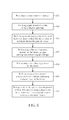
- Step 101 is performed to provide a semiconductor substrate 12 , such as silicon substrate.
- Step 103 is performed to form a gate structure 14 on the substrate 12 .
- the gate structure 14 may include a gate dielectric 14 a , a gate electrode 14 b , and a spacer 14 c .
- the spacer 14 c may be a single layer or a multilayer.
- a lightly-doped source/drain (LDD) region 15 may be optionally formed through for example ion implantation.
- LDD lightly-doped source/drain
- Step 105 is performed to form recesses 17 in the substrate 12 beside the gate structure 14 through an etching process, as shown in FIG. 4 .
- the shape of the recess in the present invention is not particularly limited and can be designed as required.
- the cross section of the recess may have a shape of polygon, for example, a polygon having four or more sides, such as octagon, hexagon, diamond shape, or pentagon.
- the polygon may have at least one angle further in a shape of curved angle or chamfered angle as desired.
- Step 107 is carried out to perform a thermal treatment process on the recesses 17 in a gas atmosphere comprising an inert gas at a first temperature.
- Amain objective of the thermal treatment process at high temperature is to destroy the adsorption or bonding of hydrogen to avoid or reduce influence of hydrogen to silicon, and thus it is not necessary for the thermal treatment to be long.
- conventional rapid thermal process, spike thermal process, or spike laser thermal process may be utilized.
- the first temperature may be in a range from 850° C. to 1050° C., and preferably about 930° C. If the time for the thermal treatment is long, other elements on the substrate may be badly affected, and accordingly such situation should be avoided.
- the thermal treatment is performed in a gas atmosphere comprising an inert gas.
- the gas atmosphere may be one which is frequently utilized in a conventional semiconductor manufacturing process.
- the gas atmosphere may be one, under normal pressure (1 atm), including an inert gas (which may be a single gas or a gas mixture) in a high concentration and an oxygen gas in an extremely low concentration.
- the inert gas may include nitrogen gas, helium, argon, and the like.
- the oxygen gas in an extremely low concentration is an amount of oxygen gas which typically and inevitably exists in the high-concentration inert gas prepared by the current technology.
- the concentration of the oxygen gas may be less than 100 ppm. Therefore, the situation that an extremely low concentration of oxygen gas included in the gas atmosphere comprising an inert gas is not excluded from the present invention.
- Step 108 may be performed optionally to wet-clean the recesses 17 .
- Cleaning solution may include for example a diluted hydrogen fluoride solution, which is commonly utilized to remove native oxide layer in the industry.
- Step 109 is carried out to perform an epitaxy growth process at a second temperature to grow a silicon-containing epitaxial layer 24 in each recess 17 .
- the epitaxy growth process may be for example a selective epitaxy growth process.
- the silicon-containing epitaxial layer 24 may grow along the surface of the recess 17 and slightly protrude from the up surface of the substrate 12 .
- the silicon-containing epitaxial layer may include for example those materials applicable to conventional strained silicon technology, such as silicon germanium (SiGe) or silicon carbide (SiC).
- the amount of germanium or carbon in the epitaxial layer may be as desired, for example, in a range from more than 0% to 50%, based on a total atom amount as 100%.
- the second temperature employed in the epitaxy growth process is preferably lower than the first temperature employed in the thermal treatment for the recess, but not limited thereto.
- the second temperature may be for example 600° C. to 900° C.
- the substrate is pre-baked at 800° C., and the epitaxy growth is carried out in a range from 600° C. to 650° C.
- Step 111 to form a source/drain may be performed during or after the epitaxy growth process of Step 109 .
- the case that Step 111 and Step 109 are performed at the same time may be as follows for example.
- One is that the dopant of a desired concentration and the silicon-containing epitaxial material are allowed to epitaxially deposit within the recesses 17 together, to form source/drain regions.
- the concentration of the dopant may be varied by design according to the depth of the dopant in the epitaxial layer.
- the dopant may be from the substrate 12 (for example the source of the dopant may be implanted into the substrate 12 beside the gate structure 14 through ion implantation after the aforesaid spacer 14 c is formed) and diffuse upon being heated during the epitaxial growth process to be incorporated into the silicon-containing epitaxial layer 24 to form source/drain regions.
- the case that Step 111 is performed following the epitaxy growth process of Step 109 may be for example that the dopant is doped into the silicon-containing epitaxial layer 24 through an ion implantation carried out on the silicon-containing epitaxial layer 24 to form source/drain regions.
- a self-aligned metal silicide (salicide) process may be performed to form a metal silicide layer 20 , such as a nickel silicide layer, on the silicon-containing epitaxial layer 24 and the gate electrode 14 b (if it is polysilicon), giving a semiconductor structure 30 as shown in FIG. 5 .
Abstract
A method of fabricating a semiconductor structure, in which after an etching process is performed to form at least one recess within a semiconductor beside a gate structure, a thermal treatment is performed on the recess in a gas atmosphere including an inert gas before a silicon-containing epitaxial layer is formed in the recess through an epitaxy growth process.
Description
1. Field of the Invention
The present invention relates to a method of fabricating a semiconductor structure, and particularly to a method of fabricating a semiconductor structure during which rounding problem of an epitaxial layer can be avoided or reduced.
2. Description of the Prior Art
As the semiconductor processes advance to very deep sub micron era such as 65-nm node, even 28 nm or beyond, how to increase the driving current for MOS transistors has become a critical issue. In order to improve device performance, strained-silicon technology has been developed. Putting a strain on a semiconductor crystal alters the speed at which charges move through that crystal. Strain makes MOS transistors work better by enabling electrical charges, such as electrons, to pass more easily through the silicon lattice of the gate channel.
One of the methods to put a strain on the silicon lattice of the gate channel is that combining a selective epitaxial growth (SEG) technology. Recesses are formed in the substrate beside the gate structure and then an epitaxial layer, such as silicon germanium (SiGe) layer having a crystal lattice arrangement the same as that of the substrate is formed within the recesses through the epitaxial growth process to serve as a source/drain, so as to apply a stress to the crystal lattice of the gate channel.
Therefore, there is still a need for a novel method of fabricating a semiconductor structure to solve the aforesaid issue.
An objective of the present invention is to provide a method of fabricating a semiconductor structure to avoid or reduce the rounding of the shape of the epitaxial layer.
The method of fabricating a semiconductor structure according to the present invention comprises steps as follows. First, a semiconductor substrate is provided. Next, a gate structure is formed on the semiconductor substrate. An etching process is performed to form at least one recess within the semiconductor substrate beside the gate structure. Thereafter, a thermal treatment process is performed on the recess in a gas atmosphere including an inert gas at a first temperature. After the thermal treatment process is performed, an epitaxy growth process is performed at a second temperature to form a silicon-containing epitaxial layer in the recess. During or after the epitaxy growth process, a dopant is incorporated into the silicon-containing epitaxial layer to form a source/drain region.
Without being bound to a theory, since, in the present invention, the recess is subject to a thermal treatment process in a gas atmosphere including an inert gas after it is formed, to alter or modify the bonding or adsorption relation of hydrogen (including atoms or ions) to the silicon of the semiconductor substrate, for example, to result in desorption of the hydrogen or alteration of the bonding type between the hydrogen and the silicon, such that the affect of the hydrogen during the subsequent epitaxy growth process can be alleviated or avoided. Accordingly, the resultant silicon-containing epitaxial layer grown in the recess may have a shape approximating to a designed or desired shape.
These and other objectives of the present invention will no doubt become obvious to those of ordinary skill in the art after reading the following detailed description of the preferred embodiment that is illustrated in the various figures and drawings.
The inventors investigated the rounding issue occurred in the conventional method and discovered that it may be resulted from the affect of the hydrogen to silicon migration at the high temperature of the epitaxy growth process. As shown in the presumed model of FIG. 2, hydrogen atoms or ions, provided from ambient atmosphere, substance from previous process, or cleaning solution containing hydrogen gas (H2), hydrogen atoms, or hydrogen ions, are adsorbed on surface of the silicon substrate 13 or form chemical bonds with silicon atoms, especially at steps or corners of the silicon substrate 13. The hydrogen may trigger the migration of silicon atoms. Accordingly, when an epitaxy growth process is being carried out, silicon atoms located at these steps or in these corners migrate due to the existence of the hydrogen, such that the resultant epitaxial layer is significantly influenced to have a shape different from the shape of the recess originally formed. It may be noted that the word “hydrogen” is used sometimes herein to encompass hydrogen gas, hydrogen atom, and/or hydrogen ion for concise description.
For resolving the above-mentioned issue, a method of fabricating a semiconductor structure the present invention is provided and featured in that, after the recess is formed, a high-temperature thermal treatment is performed on the recess in a gas atmosphere including an inert gas to reduce or avoid silicon migration triggered by hydrogen during subsequent high-temperature epitaxy growth process. Presumably, high-temperature thermal treatment might alternate the adsorption or the bonding of the hydrogen within the recess (especially those hydrogen atoms located at the steps and in the corners) to the silicon. For example, the hydrogen is desorbed or the bonding type is altered, such that the hydrogen can not trigger the silicon migration anymore. In another presumption, the alternation of the adsorption or the bonding of the hydrogen might be resulted from a reaction with high-temperature oxygen. As a result, the method of the present invention may be advantageously utilized to fabricate MOS transistor structures, including pMOS and nMOS.
An embodiment of the method of fabricating a semiconductor structure according to the present invention is described hereinafter referring to FIG. 3 together with FIGS. 4 and 5 . First, Step 101 is performed to provide a semiconductor substrate 12, such as silicon substrate. Next, Step 103 is performed to form a gate structure 14 on the substrate 12. The gate structure 14 may include a gate dielectric 14 a, a gate electrode 14 b, and a spacer 14 c. The spacer 14 c may be a single layer or a multilayer. Before the spacer 14 c is formed, a lightly-doped source/drain (LDD) region 15 may be optionally formed through for example ion implantation.
Thereafter, Step 105 is performed to form recesses 17 in the substrate 12 beside the gate structure 14 through an etching process, as shown in FIG. 4 . The shape of the recess in the present invention is not particularly limited and can be designed as required. For example, the cross section of the recess may have a shape of polygon, for example, a polygon having four or more sides, such as octagon, hexagon, diamond shape, or pentagon. The polygon may have at least one angle further in a shape of curved angle or chamfered angle as desired.
Thereafter, Step 107 is carried out to perform a thermal treatment process on the recesses 17 in a gas atmosphere comprising an inert gas at a first temperature. Amain objective of the thermal treatment process at high temperature is to destroy the adsorption or bonding of hydrogen to avoid or reduce influence of hydrogen to silicon, and thus it is not necessary for the thermal treatment to be long. For example, conventional rapid thermal process, spike thermal process, or spike laser thermal process may be utilized. The first temperature may be in a range from 850° C. to 1050° C., and preferably about 930° C. If the time for the thermal treatment is long, other elements on the substrate may be badly affected, and accordingly such situation should be avoided. The thermal treatment is performed in a gas atmosphere comprising an inert gas. The gas atmosphere may be one which is frequently utilized in a conventional semiconductor manufacturing process. For example, the gas atmosphere may be one, under normal pressure (1 atm), including an inert gas (which may be a single gas or a gas mixture) in a high concentration and an oxygen gas in an extremely low concentration. The inert gas may include nitrogen gas, helium, argon, and the like. The oxygen gas in an extremely low concentration is an amount of oxygen gas which typically and inevitably exists in the high-concentration inert gas prepared by the current technology. For example, the concentration of the oxygen gas may be less than 100 ppm. Therefore, the situation that an extremely low concentration of oxygen gas included in the gas atmosphere comprising an inert gas is not excluded from the present invention.
Furthermore, as shown in FIG. 6 , in another embodiment of the present invention, after the thermal treatment process in Step 107 is performed, Step 108 may be performed optionally to wet-clean the recesses 17. Cleaning solution may include for example a diluted hydrogen fluoride solution, which is commonly utilized to remove native oxide layer in the industry.
Following Step 107 or Step 108 (if performed), Step 109 is carried out to perform an epitaxy growth process at a second temperature to grow a silicon-containing epitaxial layer 24 in each recess 17. The epitaxy growth process may be for example a selective epitaxy growth process. The silicon-containing epitaxial layer 24 may grow along the surface of the recess 17 and slightly protrude from the up surface of the substrate 12. The silicon-containing epitaxial layer may include for example those materials applicable to conventional strained silicon technology, such as silicon germanium (SiGe) or silicon carbide (SiC). The amount of germanium or carbon in the epitaxial layer may be as desired, for example, in a range from more than 0% to 50%, based on a total atom amount as 100%. The second temperature employed in the epitaxy growth process is preferably lower than the first temperature employed in the thermal treatment for the recess, but not limited thereto. The second temperature may be for example 600° C. to 900° C. For example, the substrate is pre-baked at 800° C., and the epitaxy growth is carried out in a range from 600° C. to 650° C.
Step 111 to form a source/drain may be performed during or after the epitaxy growth process of Step 109. The case that Step 111 and Step 109 are performed at the same time may be as follows for example. One is that the dopant of a desired concentration and the silicon-containing epitaxial material are allowed to epitaxially deposit within the recesses 17 together, to form source/drain regions. The concentration of the dopant may be varied by design according to the depth of the dopant in the epitaxial layer. Another is that the dopant may be from the substrate 12 (for example the source of the dopant may be implanted into the substrate 12 beside the gate structure 14 through ion implantation after the aforesaid spacer 14 c is formed) and diffuse upon being heated during the epitaxial growth process to be incorporated into the silicon-containing epitaxial layer 24 to form source/drain regions. Alternatively, the case that Step 111 is performed following the epitaxy growth process of Step 109 may be for example that the dopant is doped into the silicon-containing epitaxial layer 24 through an ion implantation carried out on the silicon-containing epitaxial layer 24 to form source/drain regions.
Thereafter, a self-aligned metal silicide (salicide) process may be performed to form a metal silicide layer 20, such as a nickel silicide layer, on the silicon-containing epitaxial layer 24 and the gate electrode 14 b (if it is polysilicon), giving a semiconductor structure 30 as shown in FIG. 5 .
Those skilled in the art will readily observe that numerous modifications and alterations of the device and method may be made while retaining the teachings of the invention.
Claims (11)
1. A method of fabricating a semiconductor structure, comprising:
providing a semiconductor substrate;
forming a gate structure on the semiconductor substrate;
performing an etching process to form at least one recess within the semiconductor substrate beside the gate structure;
performing a thermal treatment process on the recess in a gas atmosphere comprising an inert gas at a first temperature;
after performing the thermal treatment process, wet-cleaning the recess;
after wet-cleaning the recess, performing a pre-bake process on the recess at a second temperature lower than the first temperature;
after performing the pre-bake process, performing an epitaxy growth process at a third temperature lower than the first temperature to form a silicon-containing epitaxial layer in the recess; and
during or after the epitaxy growth process, incorporating a dopant into the silicon-containing epitaxial layer to form a source/drain region.
2. The method according to claim 1 , wherein the thermal treatment process comprises a rapid thermal process, a spike thermal process, or a spike laser thermal process.
3. The method according to claim 1 , wherein one cross section of the recess is substantially in a shape of polygon.
4. The method according to claim 3 , wherein the polygon has at least one angle in a shape of curved angle or chamfered angle.
5. The method according to claim 1 , wherein the epitaxy growth process comprises a selective epitaxy growth process.
6. The method according to claim 1 , further comprising:
performing a self-aligned metal silicide process to form a metal silicide layer on the silicon-containing epitaxial layer.
7. The method according to claim 1 , wherein the first temperature is in a range from 850° C. to 1050° C.
8. The method according to claim 1 , wherein the second temperature and the third temperature are each in a range from 600° C. to 900° C.
9. The method according to claim 1 , wherein the silicon-containing epitaxial layer comprises silicon-germanium (SiGe) or silicon-carbide (SiC).
10. The method according to claim 1 , wherein, forming the gate structure comprises steps of forming a gate dielectric, a gate electrode, and a spacer.
11. The method according to claim 1 , wherein wet-cleaning the recess includes utilizing a hydrogen fluoride solution to clean the recess.
Priority Applications (1)
| Application Number | Priority Date | Filing Date | Title |
|---|---|---|---|
| US13/092,990 US8324059B2 (en) | 2011-04-25 | 2011-04-25 | Method of fabricating a semiconductor structure |
Applications Claiming Priority (1)
| Application Number | Priority Date | Filing Date | Title |
|---|---|---|---|
| US13/092,990 US8324059B2 (en) | 2011-04-25 | 2011-04-25 | Method of fabricating a semiconductor structure |
Publications (2)
| Publication Number | Publication Date |
|---|---|
| US20120270377A1 US20120270377A1 (en) | 2012-10-25 |
| US8324059B2 true US8324059B2 (en) | 2012-12-04 |
Family
ID=47021651
Family Applications (1)
| Application Number | Title | Priority Date | Filing Date |
|---|---|---|---|
| US13/092,990 Active US8324059B2 (en) | 2011-04-25 | 2011-04-25 | Method of fabricating a semiconductor structure |
Country Status (1)
| Country | Link |
|---|---|
| US (1) | US8324059B2 (en) |
Cited By (47)
| Publication number | Priority date | Publication date | Assignee | Title |
|---|---|---|---|---|
| US20120153402A1 (en) * | 2010-12-21 | 2012-06-21 | Global Foundries Inc. | Embedded sigma-shaped semiconductor alloys formed in transistors by applying a uniform oxide layer prior to cavity etching |
| US8404551B2 (en) | 2010-12-03 | 2013-03-26 | Suvolta, Inc. | Source/drain extension control for advanced transistors |
| US8421162B2 (en) | 2009-09-30 | 2013-04-16 | Suvolta, Inc. | Advanced transistors with punch through suppression |
| US20130095627A1 (en) * | 2011-10-18 | 2013-04-18 | Globalfoundries Inc. | Methods of Forming Source/Drain Regions on Transistor Devices |
| US8461875B1 (en) | 2011-02-18 | 2013-06-11 | Suvolta, Inc. | Digital circuits having improved transistors, and methods therefor |
| US8525271B2 (en) | 2011-03-03 | 2013-09-03 | Suvolta, Inc. | Semiconductor structure with improved channel stack and method for fabrication thereof |
| US8530286B2 (en) | 2010-04-12 | 2013-09-10 | Suvolta, Inc. | Low power semiconductor transistor structure and method of fabrication thereof |
| US8569156B1 (en) | 2011-05-16 | 2013-10-29 | Suvolta, Inc. | Reducing or eliminating pre-amorphization in transistor manufacture |
| US8569128B2 (en) | 2010-06-21 | 2013-10-29 | Suvolta, Inc. | Semiconductor structure and method of fabrication thereof with mixed metal types |
| US8599623B1 (en) | 2011-12-23 | 2013-12-03 | Suvolta, Inc. | Circuits and methods for measuring circuit elements in an integrated circuit device |
| US8614128B1 (en) | 2011-08-23 | 2013-12-24 | Suvolta, Inc. | CMOS structures and processes based on selective thinning |
| US8629016B1 (en) | 2011-07-26 | 2014-01-14 | Suvolta, Inc. | Multiple transistor types formed in a common epitaxial layer by differential out-diffusion from a doped underlayer |
| US8637955B1 (en) | 2012-08-31 | 2014-01-28 | Suvolta, Inc. | Semiconductor structure with reduced junction leakage and method of fabrication thereof |
| US8645878B1 (en) | 2011-08-23 | 2014-02-04 | Suvolta, Inc. | Porting a circuit design from a first semiconductor process to a second semiconductor process |
| US8713511B1 (en) | 2011-09-16 | 2014-04-29 | Suvolta, Inc. | Tools and methods for yield-aware semiconductor manufacturing process target generation |
| US8735987B1 (en) | 2011-06-06 | 2014-05-27 | Suvolta, Inc. | CMOS gate stack structures and processes |
| US8748270B1 (en) | 2011-03-30 | 2014-06-10 | Suvolta, Inc. | Process for manufacturing an improved analog transistor |
| US8748986B1 (en) | 2011-08-05 | 2014-06-10 | Suvolta, Inc. | Electronic device with controlled threshold voltage |
| US8759872B2 (en) | 2010-06-22 | 2014-06-24 | Suvolta, Inc. | Transistor with threshold voltage set notch and method of fabrication thereof |
| US8796048B1 (en) | 2011-05-11 | 2014-08-05 | Suvolta, Inc. | Monitoring and measurement of thin film layers |
| US8811068B1 (en) | 2011-05-13 | 2014-08-19 | Suvolta, Inc. | Integrated circuit devices and methods |
| US8819603B1 (en) | 2011-12-15 | 2014-08-26 | Suvolta, Inc. | Memory circuits and methods of making and designing the same |
| US8816754B1 (en) | 2012-11-02 | 2014-08-26 | Suvolta, Inc. | Body bias circuits and methods |
| US8863064B1 (en) | 2012-03-23 | 2014-10-14 | Suvolta, Inc. | SRAM cell layout structure and devices therefrom |
| US8877619B1 (en) | 2012-01-23 | 2014-11-04 | Suvolta, Inc. | Process for manufacture of integrated circuits with different channel doping transistor architectures and devices therefrom |
| US8883600B1 (en) | 2011-12-22 | 2014-11-11 | Suvolta, Inc. | Transistor having reduced junction leakage and methods of forming thereof |
| US8895327B1 (en) | 2011-12-09 | 2014-11-25 | Suvolta, Inc. | Tipless transistors, short-tip transistors, and methods and circuits therefor |
| US8970289B1 (en) | 2012-01-23 | 2015-03-03 | Suvolta, Inc. | Circuits and devices for generating bi-directional body bias voltages, and methods therefor |
| US8995204B2 (en) | 2011-06-23 | 2015-03-31 | Suvolta, Inc. | Circuit devices and methods having adjustable transistor body bias |
| US8999861B1 (en) | 2011-05-11 | 2015-04-07 | Suvolta, Inc. | Semiconductor structure with substitutional boron and method for fabrication thereof |
| US9041126B2 (en) | 2012-09-21 | 2015-05-26 | Mie Fujitsu Semiconductor Limited | Deeply depleted MOS transistors having a screening layer and methods thereof |
| US9054219B1 (en) | 2011-08-05 | 2015-06-09 | Mie Fujitsu Semiconductor Limited | Semiconductor devices having fin structures and fabrication methods thereof |
| US9070477B1 (en) | 2012-12-12 | 2015-06-30 | Mie Fujitsu Semiconductor Limited | Bit interleaved low voltage static random access memory (SRAM) and related methods |
| US9093550B1 (en) | 2012-01-31 | 2015-07-28 | Mie Fujitsu Semiconductor Limited | Integrated circuits having a plurality of high-K metal gate FETs with various combinations of channel foundation structure and gate stack structure and methods of making same |
| US9093997B1 (en) | 2012-11-15 | 2015-07-28 | Mie Fujitsu Semiconductor Limited | Slew based process and bias monitors and related methods |
| US9112057B1 (en) | 2012-09-18 | 2015-08-18 | Mie Fujitsu Semiconductor Limited | Semiconductor devices with dopant migration suppression and method of fabrication thereof |
| US9112484B1 (en) | 2012-12-20 | 2015-08-18 | Mie Fujitsu Semiconductor Limited | Integrated circuit process and bias monitors and related methods |
| US9236466B1 (en) | 2011-10-07 | 2016-01-12 | Mie Fujitsu Semiconductor Limited | Analog circuits having improved insulated gate transistors, and methods therefor |
| US9268885B1 (en) | 2013-02-28 | 2016-02-23 | Mie Fujitsu Semiconductor Limited | Integrated circuit device methods and models with predicted device metric variations |
| US9299698B2 (en) | 2012-06-27 | 2016-03-29 | Mie Fujitsu Semiconductor Limited | Semiconductor structure with multiple transistors having various threshold voltages |
| US9299801B1 (en) | 2013-03-14 | 2016-03-29 | Mie Fujitsu Semiconductor Limited | Method for fabricating a transistor device with a tuned dopant profile |
| US9319013B2 (en) | 2014-08-19 | 2016-04-19 | Mie Fujitsu Semiconductor Limited | Operational amplifier input offset correction with transistor threshold voltage adjustment |
| US9406567B1 (en) | 2012-02-28 | 2016-08-02 | Mie Fujitsu Semiconductor Limited | Method for fabricating multiple transistor devices on a substrate with varying threshold voltages |
| US9431068B2 (en) | 2012-10-31 | 2016-08-30 | Mie Fujitsu Semiconductor Limited | Dynamic random access memory (DRAM) with low variation transistor peripheral circuits |
| US9478571B1 (en) | 2013-05-24 | 2016-10-25 | Mie Fujitsu Semiconductor Limited | Buried channel deeply depleted channel transistor |
| US9710006B2 (en) | 2014-07-25 | 2017-07-18 | Mie Fujitsu Semiconductor Limited | Power up body bias circuits and methods |
| US10074568B2 (en) | 2009-09-30 | 2018-09-11 | Mie Fujitsu Semiconductor Limited | Electronic devices and systems, and methods for making and using same |
Families Citing this family (4)
| Publication number | Priority date | Publication date | Assignee | Title |
|---|---|---|---|---|
| US20170141228A1 (en) * | 2015-11-16 | 2017-05-18 | Taiwan Semiconductor Manufacturing Co., Ltd. | Field effect transistor and manufacturing method thereof |
| CN110828300B (en) * | 2019-11-25 | 2022-03-18 | 上海华力集成电路制造有限公司 | Epitaxial process |
| US11271096B2 (en) * | 2020-04-01 | 2022-03-08 | Taiwan Semiconductor Manufacturing Co., Ltd. | Method for forming fin field effect transistor device structure |
| US11626288B2 (en) * | 2021-07-30 | 2023-04-11 | Applied Materials, Inc. | Integrated contact silicide with tunable work functions |
Citations (125)
| Publication number | Priority date | Publication date | Assignee | Title |
|---|---|---|---|---|
| US4891303A (en) | 1988-05-26 | 1990-01-02 | Texas Instruments Incorporated | Trilayer microlithographic process using a silicon-based resist as the middle layer |
| US5217910A (en) | 1990-11-05 | 1993-06-08 | Mitsubishi Denki Kabushiki Kaisha | Method of fabricating semiconductor device having sidewall spacers and oblique implantation |
| US5273930A (en) | 1992-09-03 | 1993-12-28 | Motorola, Inc. | Method of forming a non-selective silicon-germanium epitaxial film |
| US5356830A (en) | 1988-09-19 | 1994-10-18 | Kabushiki Kaisha Tobshiba | Semiconductor device and its manufacturing method |
| US5372957A (en) | 1993-07-22 | 1994-12-13 | Taiwan Semiconductor Manufacturing Company | Multiple tilted angle ion implantation MOSFET method |
| US5385630A (en) | 1993-06-29 | 1995-01-31 | Digital Equipment Corporation | Process for increasing sacrificial oxide etch rate to reduce field oxide loss |
| US5399506A (en) | 1992-08-13 | 1995-03-21 | Sony Corporation | Semiconductor fabricating process |
| US5625217A (en) | 1992-12-11 | 1997-04-29 | Intel Corporation | MOS transistor having a composite gate electrode and method of fabrication |
| US5777364A (en) | 1992-11-30 | 1998-07-07 | International Business Machines Corporation | Graded channel field effect transistor |
| US5783479A (en) | 1997-06-23 | 1998-07-21 | National Science Council | Structure and method for manufacturing improved FETs having T-shaped gates |
| US5793090A (en) | 1997-01-10 | 1998-08-11 | Advanced Micro Devices, Inc. | Integrated circuit having multiple LDD and/or source/drain implant steps to enhance circuit performance |
| US5960322A (en) | 1997-12-19 | 1999-09-28 | Advanced Micro Devices, Inc. | Suppression of boron segregation for shallow source and drain junctions in semiconductors |
| US6030874A (en) | 1997-01-21 | 2000-02-29 | Texas Instruments Incorporated | Doped polysilicon to retard boron diffusion into and through thin gate dielectrics |
| US6048756A (en) | 1997-07-31 | 2000-04-11 | Electronics And Telecommunications Research Institute | Method for making a silicon-on-insulator MOS transistor using a selective SiGe epitaxy |
| US6074954A (en) | 1998-08-31 | 2000-06-13 | Applied Materials, Inc | Process for control of the shape of the etch front in the etching of polysilicon |
| US6100171A (en) | 1998-03-03 | 2000-08-08 | Advanced Micro Devices, Inc. | Reduction of boron penetration by laser anneal removal of fluorine |
| US6110787A (en) | 1999-09-07 | 2000-08-29 | Chartered Semiconductor Manufacturing Ltd. | Method for fabricating a MOS device |
| US6165881A (en) | 1998-10-23 | 2000-12-26 | Taiwan Semiconductor Manufacturing Company | Method of forming salicide poly gate with thin gate oxide and ultra narrow gate width |
| US6165826A (en) | 1994-12-23 | 2000-12-26 | Intel Corporation | Transistor with low resistance tip and method of fabrication in a CMOS process |
| US6191052B1 (en) | 1999-01-25 | 2001-02-20 | Taiwan Semiconductor Manufacturing Company | Method for fabricating an ultra-shallow junction with low resistance using a screen oxide formed by poly re-oxidation in a nitrogen containing atmosphere |
| US6228730B1 (en) | 1999-04-28 | 2001-05-08 | United Microelectronics Corp. | Method of fabricating field effect transistor |
| US6274447B1 (en) | 1996-03-22 | 2001-08-14 | Seiko Epson Corporation | Semiconductor device comprising a MOS element and a fabrication method thereof |
| US6355533B2 (en) | 1999-12-24 | 2002-03-12 | Hyundai Electronics Industries Co., Ltd. | Method for manufacturing semiconductor device |
| US6365476B1 (en) | 2000-10-27 | 2002-04-02 | Ultratech Stepper, Inc. | Laser thermal process for fabricating field-effect transistors |
| US6368926B1 (en) | 2000-03-13 | 2002-04-09 | Advanced Micro Devices, Inc. | Method of forming a semiconductor device with source/drain regions having a deep vertical junction |
| US6444591B1 (en) | 2000-09-30 | 2002-09-03 | Newport Fab, Llc | Method for reducing contamination prior to epitaxial growth and related structure |
| US20020160587A1 (en) | 2001-04-30 | 2002-10-31 | Basanth Jagannathan | Method to increase carbon and boron doping concentrations in Si and SiGe films |
| US20020182423A1 (en) | 2001-04-20 | 2002-12-05 | International Business Machines Corporation | Epitaxial and polycrystalline growth of Si1-x-yGexCy and Si1-yCy alloy layers on Si by UHV-CVD |
| US6537370B1 (en) | 1998-09-10 | 2003-03-25 | FRANCE TéLéCOM | Process for obtaining a layer of single-crystal germanium on a substrate of single-crystal silicon, and products obtained |
| US6544822B2 (en) | 2000-06-21 | 2003-04-08 | Hynix Semiconductor, Inc. | Method for fabricating MOSFET device |
| US6605498B1 (en) | 2002-03-29 | 2003-08-12 | Intel Corporation | Semiconductor transistor having a backfilled channel material |
| US6613695B2 (en) | 2000-11-24 | 2003-09-02 | Asm America, Inc. | Surface preparation prior to deposition |
| US6621131B2 (en) | 2001-11-01 | 2003-09-16 | Intel Corporation | Semiconductor transistor having a stressed channel |
| US6624068B2 (en) | 2001-08-24 | 2003-09-23 | Texas Instruments Incorporated | Polysilicon processing using an anti-reflective dual layer hardmask for 193 nm lithography |
| US20030181005A1 (en) | 2002-03-19 | 2003-09-25 | Kiyota Hachimine | Semiconductor device and a method of manufacturing the same |
| US6632718B1 (en) | 1998-07-15 | 2003-10-14 | Texas Instruments Incorporated | Disposable spacer technology for reduced cost CMOS processing |
| US20030203599A1 (en) | 2000-03-27 | 2003-10-30 | Matsushita Electric Industrial Co. , Ltd. | Semiconductor wafer and method for fabricating the same |
| US6642122B1 (en) | 2002-09-26 | 2003-11-04 | Advanced Micro Devices, Inc. | Dual laser anneal for graded halo profile |
| US6664156B1 (en) | 2002-07-31 | 2003-12-16 | Chartered Semiconductor Manufacturing, Ltd | Method for forming L-shaped spacers with precise width control |
| US6676764B2 (en) | 2001-04-30 | 2004-01-13 | Hynix Semiconductor Inc. | Method for cleaning a substrate in selective epitaxial growth process |
| US6703271B2 (en) | 2001-11-30 | 2004-03-09 | Taiwan Semiconductor Manufacturing Company | Complementary metal oxide semiconductor transistor technology using selective epitaxy of a strained silicon germanium layer |
| US20040045499A1 (en) | 2002-06-10 | 2004-03-11 | Amberwave Systems Corporation | Source and drain elements |
| US20040067631A1 (en) | 2002-10-03 | 2004-04-08 | Haowen Bu | Reduction of seed layer roughness for use in forming SiGe gate electrode |
| US6777275B1 (en) | 2000-11-15 | 2004-08-17 | Advanced Micro Devices, Inc. | Single anneal for dopant activation and silicide formation |
| US6806151B2 (en) | 2001-12-14 | 2004-10-19 | Texas Instruments Incorporated | Methods and apparatus for inducing stress in a semiconductor device |
| US6809402B1 (en) | 2002-08-14 | 2004-10-26 | Advanced Micro Devices, Inc. | Reflowable-doped HDP film |
| US6858506B2 (en) | 2002-08-08 | 2005-02-22 | Macronix International Co., Ltd. | Method for fabricating locally strained channel |
| US6864135B2 (en) | 2002-10-31 | 2005-03-08 | Freescale Semiconductor, Inc. | Semiconductor fabrication process using transistor spacers of differing widths |
| US6869867B2 (en) | 1997-10-01 | 2005-03-22 | Kabushiki Kaisha Toshiba | Semiconductor device comprising metal silicide films formed to cover gate electrode and source-drain diffusion layers and method of manufacturing the same wherein the silicide on gate is thicker than on source-drain |
| US20050070076A1 (en) | 2001-10-26 | 2005-03-31 | Dion Michel Maurice | Method of depositing high-quality sige on sige substrates |
| US20050079692A1 (en) | 2003-10-10 | 2005-04-14 | Applied Materials, Inc. | Methods to fabricate MOSFET devices using selective deposition process |
| US20050082616A1 (en) | 2003-10-20 | 2005-04-21 | Huajie Chen | High performance stress-enhanced MOSFETs using Si:C and SiGe epitaxial source/drain and method of manufacture |
| US6887762B1 (en) | 1998-11-12 | 2005-05-03 | Intel Corporation | Method of fabricating a field effect transistor structure with abrupt source/drain junctions |
| US6887751B2 (en) | 2003-09-12 | 2005-05-03 | International Business Machines Corporation | MOSFET performance improvement using deformation in SOI structure |
| US6891192B2 (en) | 2003-08-04 | 2005-05-10 | International Business Machines Corporation | Structure and method of making strained semiconductor CMOS transistors having lattice-mismatched semiconductor regions underlying source and drain regions |
| US20050139231A1 (en) | 2003-12-31 | 2005-06-30 | Commissariat A L'energie Atomique | Method of wet cleaning a surface, especially of a material of the silicon-germanium type |
| US6930007B2 (en) | 2003-09-15 | 2005-08-16 | Texas Instruments Incorporated | Integration of pre-S/D anneal selective nitride/oxide composite cap for improving transistor performance |
| US6946350B2 (en) | 2003-12-31 | 2005-09-20 | Intel Corporation | Controlled faceting of source/drain regions |
| US6949482B2 (en) | 2003-12-08 | 2005-09-27 | Intel Corporation | Method for improving transistor performance through reducing the salicide interface resistance |
| US20050260830A1 (en) | 2004-03-25 | 2005-11-24 | Doo-Won Kwon | Methods of fabricating a semiconductor device using a dilute aqueous solution of an ammonia and peroxide mixture |
| US6972461B1 (en) | 2004-06-30 | 2005-12-06 | International Business Machines Corporation | Channel MOSFET with strained silicon channel on strained SiGe |
| US20050287752A1 (en) | 2004-06-24 | 2005-12-29 | Applied Materials, Inc. | Methods for forming a transistor |
| US20050285193A1 (en) | 2004-06-28 | 2005-12-29 | Lee Sung-Young | Semiconductor device and method of manufacturing same |
| US6991979B2 (en) | 2003-09-22 | 2006-01-31 | International Business Machines Corporation | Method for avoiding oxide undercut during pre-silicide clean for thin spacer FETs |
| US6991991B2 (en) | 2003-11-12 | 2006-01-31 | United Microelectronics Corp. | Method for preventing to form a spacer undercut in SEG pre-clean process |
| US20060051922A1 (en) | 2004-09-09 | 2006-03-09 | Taiwan Semiconductor Manufacturing Company, Ltd. | Strained silicon device manufacturing method |
| US20060057859A1 (en) | 2004-09-16 | 2006-03-16 | International Business Machines Corporation | Buffer layer for selective SiGe growth for uniform nucleation |
| US20060076627A1 (en) | 2004-10-12 | 2006-04-13 | International Business Machines Corporation | Ultra shallow junction formation by epitaxial interface limited diffusion |
| US7033895B2 (en) | 2003-05-14 | 2006-04-25 | Samsung Electronics Co., Ltd. | Method of fabricating a MOS transistor with elevated source/drain structure using a selective epitaxial growth process |
| US20060088968A1 (en) | 2004-06-17 | 2006-04-27 | Samsung Electronics Co., Ltd. | Methods of fabricating a semiconductor device using a selective epitaxial growth technique |
| US7037773B2 (en) | 2004-03-29 | 2006-05-02 | United Microelectronics Corp. | Method of manufacturing metal-oxide-semiconductor transistor |
| US20060115949A1 (en) | 2004-12-01 | 2006-06-01 | Freescale Semiconductor, Inc. | Semiconductor fabrication process including source/drain recessing and filling |
| US7060576B2 (en) | 2003-10-24 | 2006-06-13 | Intel Corporation | Epitaxially deposited source/drain |
| US7060579B2 (en) | 2004-07-29 | 2006-06-13 | Texas Instruments Incorporated | Increased drive current by isotropic recess etch |
| US20060134872A1 (en) | 2004-12-17 | 2006-06-22 | Hattendorf Michael L | Strained NMOS transistor featuring deep carbon doped regions and raised donor doped source and drain |
| US20060138398A1 (en) * | 2004-12-28 | 2006-06-29 | Fujitsu Limited | Semiconductor device and fabrication method thereof |
| US7112495B2 (en) | 2003-08-15 | 2006-09-26 | Taiwan Semiconductor Manufacturing Company, Ltd. | Structure and method of a strained channel transistor and a second semiconductor component in an integrated circuit |
| US7118952B2 (en) | 2004-07-14 | 2006-10-10 | Taiwan Semiconductor Manufacturing Co., Ltd. | Method of making transistor with strained source/drain |
| US20060228842A1 (en) | 2005-04-07 | 2006-10-12 | Freescale Semiconductor, Inc. | Transistor fabrication using double etch/refill process |
| US20060231826A1 (en) | 2005-04-18 | 2006-10-19 | Toshiba America Electronic Components, Inc. | Step-embedded SiGe structure for PFET mobility enhancement |
| US20060258126A1 (en) | 2003-02-04 | 2006-11-16 | Sumco Corporation | Semiconductor substrate, field-effect transistor, and their production methods |
| US20060281288A1 (en) | 2005-06-13 | 2006-12-14 | Fujitsu Limited | Semiconductor device fabrication method |
| US20060292779A1 (en) | 2004-09-29 | 2006-12-28 | International Business Machines Corporation | Structure and method for making strained channel field effect transistor using sacrificial spacer |
| US20060292783A1 (en) | 2005-02-28 | 2006-12-28 | Young-Eun Lee | CMOS transistor and method of manufacturing the same |
| US7169675B2 (en) | 2004-07-07 | 2007-01-30 | Chartered Semiconductor Manufacturing, Ltd | Material architecture for the fabrication of low temperature transistor |
| US20070023847A1 (en) | 2005-07-26 | 2007-02-01 | Samsung Electronics Co., Ltd. | Semiconductor device and method of manufacturing the same |
| US7176504B1 (en) | 2005-09-28 | 2007-02-13 | United Microelectronics Corp. | SiGe MOSFET with an erosion preventing Six1Gey1 layer |
| US20070034906A1 (en) | 2005-08-10 | 2007-02-15 | Taiwan Semiconductor Manufacturing Company, Ltd. | MOS devices with reduced recess on substrate surface |
| US7183596B2 (en) | 2005-06-22 | 2007-02-27 | Taiwan Semiconductor Manufacturing Company, Ltd. | Composite gate structure in an integrated circuit |
| US20070049014A1 (en) | 2005-08-25 | 2007-03-01 | Ming-Tsung Chen | Method of performing salicide processes on MOS transistors |
| US20070072353A1 (en) | 2005-09-23 | 2007-03-29 | Chih-Ning Wu | Method of fabricating strained-silicon transistors and strained-silicon CMOS transistors |
| US7202124B2 (en) | 2004-10-01 | 2007-04-10 | Massachusetts Institute Of Technology | Strained gettering layers for semiconductor processes |
| US7217627B2 (en) | 2003-09-18 | 2007-05-15 | Dongbu Electronics Co., Ltd. | Semiconductor devices having diffusion barrier regions and halo implant regions and methods of fabricating the same |
| US20070128783A1 (en) | 2005-12-06 | 2007-06-07 | Shyh-Fann Ting | Method for fabricating strained-silicon cmos transistors |
| US20070128786A1 (en) | 2003-11-25 | 2007-06-07 | Taiwan Semiconductor Manufacturing Company, Ltd. | Semiconductor device having high drive current and method of manufacture therefor |
| US20070166929A1 (en) | 2006-01-18 | 2007-07-19 | Sumco Corporation | Method of producing semiconductor wafer |
| US7259050B2 (en) | 2004-04-29 | 2007-08-21 | Taiwan Semiconductor Manufacturing Company, Ltd. | Semiconductor device and method of making the same |
| US7288822B1 (en) | 2006-04-07 | 2007-10-30 | United Microelectronics Corp. | Semiconductor structure and fabricating method thereof |
| US20070262396A1 (en) | 2006-04-25 | 2007-11-15 | International Business Machines Corporation | Transistors Having V-shape Source/Drain Metal Contacts |
| US20080014688A1 (en) | 2006-07-06 | 2008-01-17 | Voon-Yew Thean | Selective uniaxial stress modification for use with strained silicon on insulator integrated circuit |
| US7335959B2 (en) | 2005-01-06 | 2008-02-26 | Intel Corporation | Device with stepped source/drain region profile |
| US20080076236A1 (en) | 2006-09-21 | 2008-03-27 | Jih-Shun Chiang | Method for forming silicon-germanium epitaxial layer |
| US20080085577A1 (en) | 2006-10-05 | 2008-04-10 | Hung-Lin Shih | Method of manufacturing complementary metal oxide semiconductor transistor |
| US20080116525A1 (en) | 2006-11-16 | 2008-05-22 | United Microelectronics Corp. | Complementary metal-oxide-semiconductor device |
| US20080124874A1 (en) * | 2006-11-03 | 2008-05-29 | Samsung Electronics Co., Ltd. | Methods of Forming Field Effect Transistors Having Silicon-Germanium Source and Drain Regions |
| US20080128746A1 (en) | 2006-12-05 | 2008-06-05 | Yin-Pin Wang | Dual-SiGe epitaxy for MOS devices |
| US20080142886A1 (en) | 2006-12-18 | 2008-06-19 | Chin-I Liao | Treatment method of semiconductor, method for manufacturing mos, and mos structure |
| US7410859B1 (en) | 2005-11-07 | 2008-08-12 | Advanced Micro Devices, Inc. | Stressed MOS device and method for its fabrication |
| US20080220579A1 (en) | 2007-03-07 | 2008-09-11 | Advanced Micro Devices, Inc. | Stress enhanced mos transistor and methods for its fabrication |
| US20080233722A1 (en) | 2007-03-23 | 2008-09-25 | United Microelectronics Corp. | Method of forming selective area compound semiconductor epitaxial layer |
| US20080233746A1 (en) | 2007-03-21 | 2008-09-25 | Hui-Ling Huang | Method for manufacturing mos transistors utilizing a hybrid hard mask |
| US20090039389A1 (en) | 2007-08-09 | 2009-02-12 | Chu-Yin Tseng | Method of fabricating metal oxide semiconductor transistor |
| US7494856B2 (en) | 2006-03-30 | 2009-02-24 | Freescale Semiconductor, Inc. | Semiconductor fabrication process using etch stop layer to optimize formation of source/drain stressor |
| US20090095992A1 (en) | 2006-12-22 | 2009-04-16 | Tomoya Sanuki | Semiconductor device including mos field effect transistor and method for manufacturing the semiconductor device |
| US20090108291A1 (en) | 2007-10-26 | 2009-04-30 | United Microelectronics Corp. | Semiconductor device and method for fabricating the same |
| US20090117715A1 (en) | 2006-02-27 | 2009-05-07 | Fujitsu Limited | Semiconductor device fabricated by selective epitaxial growth method |
| US20090124056A1 (en) | 2007-11-12 | 2009-05-14 | United Microelectronics Corp. | Method of fabricating semiconductor device |
| US20090166625A1 (en) | 2007-12-28 | 2009-07-02 | United Microelectronics Corp. | Mos device structure |
| US7560758B2 (en) | 2006-06-29 | 2009-07-14 | International Business Machines Corporation | MOSFETs comprising source/drain recesses with slanted sidewall surfaces, and methods for fabricating the same |
| US20090186475A1 (en) | 2008-01-21 | 2009-07-23 | Shyh-Fann Ting | Method of manufacturing a MOS transistor |
| US7592231B2 (en) | 2006-08-01 | 2009-09-22 | United Microelectronics Corp. | MOS transistor and fabrication thereof |
| US20090246922A1 (en) | 2008-03-27 | 2009-10-01 | Meng-Yi Wu | Method of forming cmos transistor |
| US20090278170A1 (en) | 2008-05-07 | 2009-11-12 | Yun-Chi Yang | Semiconductor device and manufacturing method thereof |
| US20100001317A1 (en) | 2008-07-03 | 2010-01-07 | Yi-Wei Chen | Cmos transistor and the method for manufacturing the same |
| US20100093147A1 (en) | 2008-10-14 | 2010-04-15 | Chin-I Liao | Method for forming a semiconductor device |
-
2011
- 2011-04-25 US US13/092,990 patent/US8324059B2/en active Active
Patent Citations (132)
| Publication number | Priority date | Publication date | Assignee | Title |
|---|---|---|---|---|
| US4891303A (en) | 1988-05-26 | 1990-01-02 | Texas Instruments Incorporated | Trilayer microlithographic process using a silicon-based resist as the middle layer |
| US5356830A (en) | 1988-09-19 | 1994-10-18 | Kabushiki Kaisha Tobshiba | Semiconductor device and its manufacturing method |
| US5217910A (en) | 1990-11-05 | 1993-06-08 | Mitsubishi Denki Kabushiki Kaisha | Method of fabricating semiconductor device having sidewall spacers and oblique implantation |
| US5399506A (en) | 1992-08-13 | 1995-03-21 | Sony Corporation | Semiconductor fabricating process |
| US5273930A (en) | 1992-09-03 | 1993-12-28 | Motorola, Inc. | Method of forming a non-selective silicon-germanium epitaxial film |
| US5777364A (en) | 1992-11-30 | 1998-07-07 | International Business Machines Corporation | Graded channel field effect transistor |
| US5625217A (en) | 1992-12-11 | 1997-04-29 | Intel Corporation | MOS transistor having a composite gate electrode and method of fabrication |
| US5783478A (en) | 1992-12-11 | 1998-07-21 | Intel Corporation | Method of frabricating a MOS transistor having a composite gate electrode |
| US5385630A (en) | 1993-06-29 | 1995-01-31 | Digital Equipment Corporation | Process for increasing sacrificial oxide etch rate to reduce field oxide loss |
| US5372957A (en) | 1993-07-22 | 1994-12-13 | Taiwan Semiconductor Manufacturing Company | Multiple tilted angle ion implantation MOSFET method |
| US6165826A (en) | 1994-12-23 | 2000-12-26 | Intel Corporation | Transistor with low resistance tip and method of fabrication in a CMOS process |
| US6274447B1 (en) | 1996-03-22 | 2001-08-14 | Seiko Epson Corporation | Semiconductor device comprising a MOS element and a fabrication method thereof |
| US5793090A (en) | 1997-01-10 | 1998-08-11 | Advanced Micro Devices, Inc. | Integrated circuit having multiple LDD and/or source/drain implant steps to enhance circuit performance |
| US6030874A (en) | 1997-01-21 | 2000-02-29 | Texas Instruments Incorporated | Doped polysilicon to retard boron diffusion into and through thin gate dielectrics |
| US5783479A (en) | 1997-06-23 | 1998-07-21 | National Science Council | Structure and method for manufacturing improved FETs having T-shaped gates |
| US6048756A (en) | 1997-07-31 | 2000-04-11 | Electronics And Telecommunications Research Institute | Method for making a silicon-on-insulator MOS transistor using a selective SiGe epitaxy |
| US6869867B2 (en) | 1997-10-01 | 2005-03-22 | Kabushiki Kaisha Toshiba | Semiconductor device comprising metal silicide films formed to cover gate electrode and source-drain diffusion layers and method of manufacturing the same wherein the silicide on gate is thicker than on source-drain |
| US5960322A (en) | 1997-12-19 | 1999-09-28 | Advanced Micro Devices, Inc. | Suppression of boron segregation for shallow source and drain junctions in semiconductors |
| US6100171A (en) | 1998-03-03 | 2000-08-08 | Advanced Micro Devices, Inc. | Reduction of boron penetration by laser anneal removal of fluorine |
| US6699763B2 (en) | 1998-07-15 | 2004-03-02 | Texas Instruments Incorporated | Disposable spacer technology for reduced cost CMOS processing |
| US6632718B1 (en) | 1998-07-15 | 2003-10-14 | Texas Instruments Incorporated | Disposable spacer technology for reduced cost CMOS processing |
| US6074954A (en) | 1998-08-31 | 2000-06-13 | Applied Materials, Inc | Process for control of the shape of the etch front in the etching of polysilicon |
| US6537370B1 (en) | 1998-09-10 | 2003-03-25 | FRANCE TéLéCOM | Process for obtaining a layer of single-crystal germanium on a substrate of single-crystal silicon, and products obtained |
| US6165881A (en) | 1998-10-23 | 2000-12-26 | Taiwan Semiconductor Manufacturing Company | Method of forming salicide poly gate with thin gate oxide and ultra narrow gate width |
| US6887762B1 (en) | 1998-11-12 | 2005-05-03 | Intel Corporation | Method of fabricating a field effect transistor structure with abrupt source/drain junctions |
| US6191052B1 (en) | 1999-01-25 | 2001-02-20 | Taiwan Semiconductor Manufacturing Company | Method for fabricating an ultra-shallow junction with low resistance using a screen oxide formed by poly re-oxidation in a nitrogen containing atmosphere |
| US6228730B1 (en) | 1999-04-28 | 2001-05-08 | United Microelectronics Corp. | Method of fabricating field effect transistor |
| US6110787A (en) | 1999-09-07 | 2000-08-29 | Chartered Semiconductor Manufacturing Ltd. | Method for fabricating a MOS device |
| US6355533B2 (en) | 1999-12-24 | 2002-03-12 | Hyundai Electronics Industries Co., Ltd. | Method for manufacturing semiconductor device |
| US6368926B1 (en) | 2000-03-13 | 2002-04-09 | Advanced Micro Devices, Inc. | Method of forming a semiconductor device with source/drain regions having a deep vertical junction |
| US20030203599A1 (en) | 2000-03-27 | 2003-10-30 | Matsushita Electric Industrial Co. , Ltd. | Semiconductor wafer and method for fabricating the same |
| US6544822B2 (en) | 2000-06-21 | 2003-04-08 | Hynix Semiconductor, Inc. | Method for fabricating MOSFET device |
| US6444591B1 (en) | 2000-09-30 | 2002-09-03 | Newport Fab, Llc | Method for reducing contamination prior to epitaxial growth and related structure |
| US6365476B1 (en) | 2000-10-27 | 2002-04-02 | Ultratech Stepper, Inc. | Laser thermal process for fabricating field-effect transistors |
| US6777275B1 (en) | 2000-11-15 | 2004-08-17 | Advanced Micro Devices, Inc. | Single anneal for dopant activation and silicide formation |
| US6613695B2 (en) | 2000-11-24 | 2003-09-02 | Asm America, Inc. | Surface preparation prior to deposition |
| US20020182423A1 (en) | 2001-04-20 | 2002-12-05 | International Business Machines Corporation | Epitaxial and polycrystalline growth of Si1-x-yGexCy and Si1-yCy alloy layers on Si by UHV-CVD |
| US6676764B2 (en) | 2001-04-30 | 2004-01-13 | Hynix Semiconductor Inc. | Method for cleaning a substrate in selective epitaxial growth process |
| US20020160587A1 (en) | 2001-04-30 | 2002-10-31 | Basanth Jagannathan | Method to increase carbon and boron doping concentrations in Si and SiGe films |
| US6624068B2 (en) | 2001-08-24 | 2003-09-23 | Texas Instruments Incorporated | Polysilicon processing using an anti-reflective dual layer hardmask for 193 nm lithography |
| US20050070076A1 (en) | 2001-10-26 | 2005-03-31 | Dion Michel Maurice | Method of depositing high-quality sige on sige substrates |
| US6621131B2 (en) | 2001-11-01 | 2003-09-16 | Intel Corporation | Semiconductor transistor having a stressed channel |
| US6861318B2 (en) | 2001-11-01 | 2005-03-01 | Intel Corporation | Semiconductor transistor having a stressed channel |
| US6703271B2 (en) | 2001-11-30 | 2004-03-09 | Taiwan Semiconductor Manufacturing Company | Complementary metal oxide semiconductor transistor technology using selective epitaxy of a strained silicon germanium layer |
| US6806151B2 (en) | 2001-12-14 | 2004-10-19 | Texas Instruments Incorporated | Methods and apparatus for inducing stress in a semiconductor device |
| US20030181005A1 (en) | 2002-03-19 | 2003-09-25 | Kiyota Hachimine | Semiconductor device and a method of manufacturing the same |
| US6605498B1 (en) | 2002-03-29 | 2003-08-12 | Intel Corporation | Semiconductor transistor having a backfilled channel material |
| US20040045499A1 (en) | 2002-06-10 | 2004-03-11 | Amberwave Systems Corporation | Source and drain elements |
| US6664156B1 (en) | 2002-07-31 | 2003-12-16 | Chartered Semiconductor Manufacturing, Ltd | Method for forming L-shaped spacers with precise width control |
| US6858506B2 (en) | 2002-08-08 | 2005-02-22 | Macronix International Co., Ltd. | Method for fabricating locally strained channel |
| US6809402B1 (en) | 2002-08-14 | 2004-10-26 | Advanced Micro Devices, Inc. | Reflowable-doped HDP film |
| US6642122B1 (en) | 2002-09-26 | 2003-11-04 | Advanced Micro Devices, Inc. | Dual laser anneal for graded halo profile |
| US20040067631A1 (en) | 2002-10-03 | 2004-04-08 | Haowen Bu | Reduction of seed layer roughness for use in forming SiGe gate electrode |
| US6864135B2 (en) | 2002-10-31 | 2005-03-08 | Freescale Semiconductor, Inc. | Semiconductor fabrication process using transistor spacers of differing widths |
| US20060258126A1 (en) | 2003-02-04 | 2006-11-16 | Sumco Corporation | Semiconductor substrate, field-effect transistor, and their production methods |
| US20060163558A1 (en) | 2003-05-14 | 2006-07-27 | Samsung Electronics, Co., Ltd. | MOS transistor with elevated source/drain structure |
| US7033895B2 (en) | 2003-05-14 | 2006-04-25 | Samsung Electronics Co., Ltd. | Method of fabricating a MOS transistor with elevated source/drain structure using a selective epitaxial growth process |
| US6891192B2 (en) | 2003-08-04 | 2005-05-10 | International Business Machines Corporation | Structure and method of making strained semiconductor CMOS transistors having lattice-mismatched semiconductor regions underlying source and drain regions |
| US7112495B2 (en) | 2003-08-15 | 2006-09-26 | Taiwan Semiconductor Manufacturing Company, Ltd. | Structure and method of a strained channel transistor and a second semiconductor component in an integrated circuit |
| US6887751B2 (en) | 2003-09-12 | 2005-05-03 | International Business Machines Corporation | MOSFET performance improvement using deformation in SOI structure |
| US6930007B2 (en) | 2003-09-15 | 2005-08-16 | Texas Instruments Incorporated | Integration of pre-S/D anneal selective nitride/oxide composite cap for improving transistor performance |
| US7217627B2 (en) | 2003-09-18 | 2007-05-15 | Dongbu Electronics Co., Ltd. | Semiconductor devices having diffusion barrier regions and halo implant regions and methods of fabricating the same |
| US6991979B2 (en) | 2003-09-22 | 2006-01-31 | International Business Machines Corporation | Method for avoiding oxide undercut during pre-silicide clean for thin spacer FETs |
| US20070082451A1 (en) | 2003-10-10 | 2007-04-12 | Samoilov Arkadii V | Methods to fabricate mosfet devices using a selective deposition process |
| US7132338B2 (en) | 2003-10-10 | 2006-11-07 | Applied Materials, Inc. | Methods to fabricate MOSFET devices using selective deposition process |
| US20050079692A1 (en) | 2003-10-10 | 2005-04-14 | Applied Materials, Inc. | Methods to fabricate MOSFET devices using selective deposition process |
| US20050082616A1 (en) | 2003-10-20 | 2005-04-21 | Huajie Chen | High performance stress-enhanced MOSFETs using Si:C and SiGe epitaxial source/drain and method of manufacture |
| US7060576B2 (en) | 2003-10-24 | 2006-06-13 | Intel Corporation | Epitaxially deposited source/drain |
| US6991991B2 (en) | 2003-11-12 | 2006-01-31 | United Microelectronics Corp. | Method for preventing to form a spacer undercut in SEG pre-clean process |
| US20070128786A1 (en) | 2003-11-25 | 2007-06-07 | Taiwan Semiconductor Manufacturing Company, Ltd. | Semiconductor device having high drive current and method of manufacture therefor |
| US6949482B2 (en) | 2003-12-08 | 2005-09-27 | Intel Corporation | Method for improving transistor performance through reducing the salicide interface resistance |
| US20050139231A1 (en) | 2003-12-31 | 2005-06-30 | Commissariat A L'energie Atomique | Method of wet cleaning a surface, especially of a material of the silicon-germanium type |
| US6946350B2 (en) | 2003-12-31 | 2005-09-20 | Intel Corporation | Controlled faceting of source/drain regions |
| US20050260830A1 (en) | 2004-03-25 | 2005-11-24 | Doo-Won Kwon | Methods of fabricating a semiconductor device using a dilute aqueous solution of an ammonia and peroxide mixture |
| US7037773B2 (en) | 2004-03-29 | 2006-05-02 | United Microelectronics Corp. | Method of manufacturing metal-oxide-semiconductor transistor |
| US7259050B2 (en) | 2004-04-29 | 2007-08-21 | Taiwan Semiconductor Manufacturing Company, Ltd. | Semiconductor device and method of making the same |
| US20060088968A1 (en) | 2004-06-17 | 2006-04-27 | Samsung Electronics Co., Ltd. | Methods of fabricating a semiconductor device using a selective epitaxial growth technique |
| US20050287752A1 (en) | 2004-06-24 | 2005-12-29 | Applied Materials, Inc. | Methods for forming a transistor |
| US20050285193A1 (en) | 2004-06-28 | 2005-12-29 | Lee Sung-Young | Semiconductor device and method of manufacturing same |
| US6972461B1 (en) | 2004-06-30 | 2005-12-06 | International Business Machines Corporation | Channel MOSFET with strained silicon channel on strained SiGe |
| US7169675B2 (en) | 2004-07-07 | 2007-01-30 | Chartered Semiconductor Manufacturing, Ltd | Material architecture for the fabrication of low temperature transistor |
| US7118952B2 (en) | 2004-07-14 | 2006-10-10 | Taiwan Semiconductor Manufacturing Co., Ltd. | Method of making transistor with strained source/drain |
| US7060579B2 (en) | 2004-07-29 | 2006-06-13 | Texas Instruments Incorporated | Increased drive current by isotropic recess etch |
| US20060051922A1 (en) | 2004-09-09 | 2006-03-09 | Taiwan Semiconductor Manufacturing Company, Ltd. | Strained silicon device manufacturing method |
| US20060057859A1 (en) | 2004-09-16 | 2006-03-16 | International Business Machines Corporation | Buffer layer for selective SiGe growth for uniform nucleation |
| US20060292779A1 (en) | 2004-09-29 | 2006-12-28 | International Business Machines Corporation | Structure and method for making strained channel field effect transistor using sacrificial spacer |
| US7202124B2 (en) | 2004-10-01 | 2007-04-10 | Massachusetts Institute Of Technology | Strained gettering layers for semiconductor processes |
| US20060076627A1 (en) | 2004-10-12 | 2006-04-13 | International Business Machines Corporation | Ultra shallow junction formation by epitaxial interface limited diffusion |
| US20060115949A1 (en) | 2004-12-01 | 2006-06-01 | Freescale Semiconductor, Inc. | Semiconductor fabrication process including source/drain recessing and filling |
| US20060134872A1 (en) | 2004-12-17 | 2006-06-22 | Hattendorf Michael L | Strained NMOS transistor featuring deep carbon doped regions and raised donor doped source and drain |
| US7667227B2 (en) | 2004-12-28 | 2010-02-23 | Fujitsu Microelectronics Limited | Semiconductor device and fabrication method thereof |
| US20060138398A1 (en) * | 2004-12-28 | 2006-06-29 | Fujitsu Limited | Semiconductor device and fabrication method thereof |
| US7335959B2 (en) | 2005-01-06 | 2008-02-26 | Intel Corporation | Device with stepped source/drain region profile |
| US20060292783A1 (en) | 2005-02-28 | 2006-12-28 | Young-Eun Lee | CMOS transistor and method of manufacturing the same |
| US20060228842A1 (en) | 2005-04-07 | 2006-10-12 | Freescale Semiconductor, Inc. | Transistor fabrication using double etch/refill process |
| US20060231826A1 (en) | 2005-04-18 | 2006-10-19 | Toshiba America Electronic Components, Inc. | Step-embedded SiGe structure for PFET mobility enhancement |
| US20060281288A1 (en) | 2005-06-13 | 2006-12-14 | Fujitsu Limited | Semiconductor device fabrication method |
| US7183596B2 (en) | 2005-06-22 | 2007-02-27 | Taiwan Semiconductor Manufacturing Company, Ltd. | Composite gate structure in an integrated circuit |
| US20070023847A1 (en) | 2005-07-26 | 2007-02-01 | Samsung Electronics Co., Ltd. | Semiconductor device and method of manufacturing the same |
| US20070034906A1 (en) | 2005-08-10 | 2007-02-15 | Taiwan Semiconductor Manufacturing Company, Ltd. | MOS devices with reduced recess on substrate surface |
| US20070049014A1 (en) | 2005-08-25 | 2007-03-01 | Ming-Tsung Chen | Method of performing salicide processes on MOS transistors |
| US20070072353A1 (en) | 2005-09-23 | 2007-03-29 | Chih-Ning Wu | Method of fabricating strained-silicon transistors and strained-silicon CMOS transistors |
| US7176504B1 (en) | 2005-09-28 | 2007-02-13 | United Microelectronics Corp. | SiGe MOSFET with an erosion preventing Six1Gey1 layer |
| US7410859B1 (en) | 2005-11-07 | 2008-08-12 | Advanced Micro Devices, Inc. | Stressed MOS device and method for its fabrication |
| US20070128783A1 (en) | 2005-12-06 | 2007-06-07 | Shyh-Fann Ting | Method for fabricating strained-silicon cmos transistors |
| US20070166929A1 (en) | 2006-01-18 | 2007-07-19 | Sumco Corporation | Method of producing semiconductor wafer |
| US20090117715A1 (en) | 2006-02-27 | 2009-05-07 | Fujitsu Limited | Semiconductor device fabricated by selective epitaxial growth method |
| US7494856B2 (en) | 2006-03-30 | 2009-02-24 | Freescale Semiconductor, Inc. | Semiconductor fabrication process using etch stop layer to optimize formation of source/drain stressor |
| US7288822B1 (en) | 2006-04-07 | 2007-10-30 | United Microelectronics Corp. | Semiconductor structure and fabricating method thereof |
| US20070262396A1 (en) | 2006-04-25 | 2007-11-15 | International Business Machines Corporation | Transistors Having V-shape Source/Drain Metal Contacts |
| US7560758B2 (en) | 2006-06-29 | 2009-07-14 | International Business Machines Corporation | MOSFETs comprising source/drain recesses with slanted sidewall surfaces, and methods for fabricating the same |
| US20080014688A1 (en) | 2006-07-06 | 2008-01-17 | Voon-Yew Thean | Selective uniaxial stress modification for use with strained silicon on insulator integrated circuit |
| US7592231B2 (en) | 2006-08-01 | 2009-09-22 | United Microelectronics Corp. | MOS transistor and fabrication thereof |
| US20080076236A1 (en) | 2006-09-21 | 2008-03-27 | Jih-Shun Chiang | Method for forming silicon-germanium epitaxial layer |
| US20080085577A1 (en) | 2006-10-05 | 2008-04-10 | Hung-Lin Shih | Method of manufacturing complementary metal oxide semiconductor transistor |
| US20080124874A1 (en) * | 2006-11-03 | 2008-05-29 | Samsung Electronics Co., Ltd. | Methods of Forming Field Effect Transistors Having Silicon-Germanium Source and Drain Regions |
| US20080116525A1 (en) | 2006-11-16 | 2008-05-22 | United Microelectronics Corp. | Complementary metal-oxide-semiconductor device |
| US20080128746A1 (en) | 2006-12-05 | 2008-06-05 | Yin-Pin Wang | Dual-SiGe epitaxy for MOS devices |
| US20080142886A1 (en) | 2006-12-18 | 2008-06-19 | Chin-I Liao | Treatment method of semiconductor, method for manufacturing mos, and mos structure |
| US20090095992A1 (en) | 2006-12-22 | 2009-04-16 | Tomoya Sanuki | Semiconductor device including mos field effect transistor and method for manufacturing the semiconductor device |
| US20080220579A1 (en) | 2007-03-07 | 2008-09-11 | Advanced Micro Devices, Inc. | Stress enhanced mos transistor and methods for its fabrication |
| US20080233746A1 (en) | 2007-03-21 | 2008-09-25 | Hui-Ling Huang | Method for manufacturing mos transistors utilizing a hybrid hard mask |
| US20080233722A1 (en) | 2007-03-23 | 2008-09-25 | United Microelectronics Corp. | Method of forming selective area compound semiconductor epitaxial layer |
| US20090039389A1 (en) | 2007-08-09 | 2009-02-12 | Chu-Yin Tseng | Method of fabricating metal oxide semiconductor transistor |
| US20090108291A1 (en) | 2007-10-26 | 2009-04-30 | United Microelectronics Corp. | Semiconductor device and method for fabricating the same |
| US20090124056A1 (en) | 2007-11-12 | 2009-05-14 | United Microelectronics Corp. | Method of fabricating semiconductor device |
| US20090166625A1 (en) | 2007-12-28 | 2009-07-02 | United Microelectronics Corp. | Mos device structure |
| US20090186475A1 (en) | 2008-01-21 | 2009-07-23 | Shyh-Fann Ting | Method of manufacturing a MOS transistor |
| US20090246922A1 (en) | 2008-03-27 | 2009-10-01 | Meng-Yi Wu | Method of forming cmos transistor |
| US20090278170A1 (en) | 2008-05-07 | 2009-11-12 | Yun-Chi Yang | Semiconductor device and manufacturing method thereof |
| US20100001317A1 (en) | 2008-07-03 | 2010-01-07 | Yi-Wei Chen | Cmos transistor and the method for manufacturing the same |
| US20100093147A1 (en) | 2008-10-14 | 2010-04-15 | Chin-I Liao | Method for forming a semiconductor device |
Non-Patent Citations (6)
| Title |
|---|
| Carl Galewski et al., "Silicon Wafer Preparation for Low-Temperature Selective Epitaxial Growth", IEEE Transactions on Semiconductor Manufacturing, vol. 3, No. 3, Aug. 1990, p. 93-98. |
| Emmanuel Augendre et al., "Elevated Source/Drain by Sacrificial Selective Epitaxy for High Performance Deep Submicron CMOS: Process Window versus Complexity", IEEE Transactions on Electron Devices, vol. 47, No. 7, Jul. 2000, p. 1484-p. 1491. |
| Junichi Murota et al., "CVD SiGe(C) Epitaxial Growth and Its Application to MOS Devices", 2001 IEEE, p. 525-p. 530. |
| Kiyotaka Miyano et al., "SPE2~Novel 700° C. Selective Epitaxial Growth Technology for Elevated Source/Drain", Extended abstracts of International Workshop on Junction Technology 2001, p. 5-2-1-p. 5-2-4. |
| Kiyotaka Miyano et al., "SPE2˜Novel 700° C. Selective Epitaxial Growth Technology for Elevated Source/Drain", Extended abstracts of International Workshop on Junction Technology 2001, p. 5-2-1-p. 5-2-4. |
| Naruhisa Miura et al., "Junction Capacitance Reduction Due to Self-Aligned Pocket Implantation in Elevated Source/Drain NMOSFETs", IEEE Transactions on Electron Devices, vol. 48, No, 9, Sep. 2001, p. 1969-p. 1974. |
Cited By (97)
| Publication number | Priority date | Publication date | Assignee | Title |
|---|---|---|---|---|
| US11062950B2 (en) | 2009-09-30 | 2021-07-13 | United Semiconductor Japan Co., Ltd. | Electronic devices and systems, and methods for making and using the same |
| US10217668B2 (en) | 2009-09-30 | 2019-02-26 | Mie Fujitsu Semiconductor Limited | Electronic devices and systems, and methods for making and using the same |
| US10074568B2 (en) | 2009-09-30 | 2018-09-11 | Mie Fujitsu Semiconductor Limited | Electronic devices and systems, and methods for making and using same |
| US11887895B2 (en) | 2009-09-30 | 2024-01-30 | United Semiconductor Japan Co., Ltd. | Electronic devices and systems, and methods for making and using the same |
| US10224244B2 (en) | 2009-09-30 | 2019-03-05 | Mie Fujitsu Semiconductor Limited | Electronic devices and systems, and methods for making and using the same |
| US9508800B2 (en) | 2009-09-30 | 2016-11-29 | Mie Fujitsu Semiconductor Limited | Advanced transistors with punch through suppression |
| US9263523B2 (en) | 2009-09-30 | 2016-02-16 | Mie Fujitsu Semiconductor Limited | Advanced transistors with punch through suppression |
| US10325986B2 (en) | 2009-09-30 | 2019-06-18 | Mie Fujitsu Semiconductor Limited | Advanced transistors with punch through suppression |
| US8421162B2 (en) | 2009-09-30 | 2013-04-16 | Suvolta, Inc. | Advanced transistors with punch through suppression |
| US8530286B2 (en) | 2010-04-12 | 2013-09-10 | Suvolta, Inc. | Low power semiconductor transistor structure and method of fabrication thereof |
| US9496261B2 (en) | 2010-04-12 | 2016-11-15 | Mie Fujitsu Semiconductor Limited | Low power semiconductor transistor structure and method of fabrication thereof |
| US9865596B2 (en) | 2010-04-12 | 2018-01-09 | Mie Fujitsu Semiconductor Limited | Low power semiconductor transistor structure and method of fabrication thereof |
| US8569128B2 (en) | 2010-06-21 | 2013-10-29 | Suvolta, Inc. | Semiconductor structure and method of fabrication thereof with mixed metal types |
| US9224733B2 (en) | 2010-06-21 | 2015-12-29 | Mie Fujitsu Semiconductor Limited | Semiconductor structure and method of fabrication thereof with mixed metal types |
| US9418987B2 (en) | 2010-06-22 | 2016-08-16 | Mie Fujitsu Semiconductor Limited | Transistor with threshold voltage set notch and method of fabrication thereof |
| US9922977B2 (en) | 2010-06-22 | 2018-03-20 | Mie Fujitsu Semiconductor Limited | Transistor with threshold voltage set notch and method of fabrication thereof |
| US8759872B2 (en) | 2010-06-22 | 2014-06-24 | Suvolta, Inc. | Transistor with threshold voltage set notch and method of fabrication thereof |
| US8686511B2 (en) | 2010-12-03 | 2014-04-01 | Suvolta, Inc. | Source/drain extension control for advanced transistors |
| US9006843B2 (en) | 2010-12-03 | 2015-04-14 | Suvolta, Inc. | Source/drain extension control for advanced transistors |
| US8404551B2 (en) | 2010-12-03 | 2013-03-26 | Suvolta, Inc. | Source/drain extension control for advanced transistors |
| US8563384B2 (en) | 2010-12-03 | 2013-10-22 | Suvolta, Inc. | Source/drain extension control for advanced transistors |
| US20120153402A1 (en) * | 2010-12-21 | 2012-06-21 | Global Foundries Inc. | Embedded sigma-shaped semiconductor alloys formed in transistors by applying a uniform oxide layer prior to cavity etching |
| US8728896B2 (en) * | 2010-12-21 | 2014-05-20 | Globalfoundries Inc. | Embedded sigma-shaped semiconductor alloys formed in transistors by applying a uniform oxide layer prior to cavity etching |
| US9985631B2 (en) | 2011-02-18 | 2018-05-29 | Mie Fujitsu Semiconductor Limited | Digital circuits having improved transistors, and methods therefor |
| US9680470B2 (en) | 2011-02-18 | 2017-06-13 | Mie Fujitsu Semiconductor Limited | Digital circuits having improved transistors, and methods therefor |
| US10250257B2 (en) | 2011-02-18 | 2019-04-02 | Mie Fujitsu Semiconductor Limited | Digital circuits having improved transistors, and methods therefor |
| US9838012B2 (en) | 2011-02-18 | 2017-12-05 | Mie Fujitsu Semiconductor Limited | Digital circuits having improved transistors, and methods therefor |
| US8461875B1 (en) | 2011-02-18 | 2013-06-11 | Suvolta, Inc. | Digital circuits having improved transistors, and methods therefor |
| US9184750B1 (en) | 2011-02-18 | 2015-11-10 | Mie Fujitsu Semiconductor Limited | Digital circuits having improved transistors, and methods therefor |
| US8525271B2 (en) | 2011-03-03 | 2013-09-03 | Suvolta, Inc. | Semiconductor structure with improved channel stack and method for fabrication thereof |
| US9111785B2 (en) | 2011-03-03 | 2015-08-18 | Mie Fujitsu Semiconductor Limited | Semiconductor structure with improved channel stack and method for fabrication thereof |
| US8748270B1 (en) | 2011-03-30 | 2014-06-10 | Suvolta, Inc. | Process for manufacturing an improved analog transistor |
| US9093469B2 (en) | 2011-03-30 | 2015-07-28 | Mie Fujitsu Semiconductor Limited | Analog transistor |
| US8796048B1 (en) | 2011-05-11 | 2014-08-05 | Suvolta, Inc. | Monitoring and measurement of thin film layers |
| US8999861B1 (en) | 2011-05-11 | 2015-04-07 | Suvolta, Inc. | Semiconductor structure with substitutional boron and method for fabrication thereof |
| US8811068B1 (en) | 2011-05-13 | 2014-08-19 | Suvolta, Inc. | Integrated circuit devices and methods |
| US9966130B2 (en) | 2011-05-13 | 2018-05-08 | Mie Fujitsu Semiconductor Limited | Integrated circuit devices and methods |
| US9741428B2 (en) | 2011-05-13 | 2017-08-22 | Mie Fujitsu Semiconductor Limited | Integrated circuit devices and methods |
| US9362291B1 (en) | 2011-05-13 | 2016-06-07 | Mie Fujitsu Semiconductor Limited | Integrated circuit devices and methods |
| US9514940B2 (en) | 2011-05-16 | 2016-12-06 | Mie Fujitsu Semiconductor Limited | Reducing or eliminating pre-amorphization in transistor manufacture |
| US9793172B2 (en) | 2011-05-16 | 2017-10-17 | Mie Fujitsu Semiconductor Limited | Reducing or eliminating pre-amorphization in transistor manufacture |
| US8937005B2 (en) | 2011-05-16 | 2015-01-20 | Suvolta, Inc. | Reducing or eliminating pre-amorphization in transistor manufacture |
| US8569156B1 (en) | 2011-05-16 | 2013-10-29 | Suvolta, Inc. | Reducing or eliminating pre-amorphization in transistor manufacture |
| US8735987B1 (en) | 2011-06-06 | 2014-05-27 | Suvolta, Inc. | CMOS gate stack structures and processes |
| US9281248B1 (en) | 2011-06-06 | 2016-03-08 | Mie Fujitsu Semiconductor Limited | CMOS gate stack structures and processes |
| US8995204B2 (en) | 2011-06-23 | 2015-03-31 | Suvolta, Inc. | Circuit devices and methods having adjustable transistor body bias |
| US8629016B1 (en) | 2011-07-26 | 2014-01-14 | Suvolta, Inc. | Multiple transistor types formed in a common epitaxial layer by differential out-diffusion from a doped underlayer |
| US8653604B1 (en) | 2011-07-26 | 2014-02-18 | Suvolta, Inc. | Multiple transistor types formed in a common epitaxial layer by differential out-diffusion from a doped underlayer |
| US8916937B1 (en) | 2011-07-26 | 2014-12-23 | Suvolta, Inc. | Multiple transistor types formed in a common epitaxial layer by differential out-diffusion from a doped underlayer |
| US8963249B1 (en) | 2011-08-05 | 2015-02-24 | Suvolta, Inc. | Electronic device with controlled threshold voltage |
| US9054219B1 (en) | 2011-08-05 | 2015-06-09 | Mie Fujitsu Semiconductor Limited | Semiconductor devices having fin structures and fabrication methods thereof |
| US8748986B1 (en) | 2011-08-05 | 2014-06-10 | Suvolta, Inc. | Electronic device with controlled threshold voltage |
| US9117746B1 (en) | 2011-08-23 | 2015-08-25 | Mie Fujitsu Semiconductor Limited | Porting a circuit design from a first semiconductor process to a second semiconductor process |
| US8806395B1 (en) | 2011-08-23 | 2014-08-12 | Suvolta, Inc. | Porting a circuit design from a first semiconductor process to a second semiconductor process |
| US8645878B1 (en) | 2011-08-23 | 2014-02-04 | Suvolta, Inc. | Porting a circuit design from a first semiconductor process to a second semiconductor process |
| US8614128B1 (en) | 2011-08-23 | 2013-12-24 | Suvolta, Inc. | CMOS structures and processes based on selective thinning |
| US9391076B1 (en) | 2011-08-23 | 2016-07-12 | Mie Fujitsu Semiconductor Limited | CMOS structures and processes based on selective thinning |
| US8713511B1 (en) | 2011-09-16 | 2014-04-29 | Suvolta, Inc. | Tools and methods for yield-aware semiconductor manufacturing process target generation |
| US9236466B1 (en) | 2011-10-07 | 2016-01-12 | Mie Fujitsu Semiconductor Limited | Analog circuits having improved insulated gate transistors, and methods therefor |
| US20130095627A1 (en) * | 2011-10-18 | 2013-04-18 | Globalfoundries Inc. | Methods of Forming Source/Drain Regions on Transistor Devices |
| US8895327B1 (en) | 2011-12-09 | 2014-11-25 | Suvolta, Inc. | Tipless transistors, short-tip transistors, and methods and circuits therefor |
| US8819603B1 (en) | 2011-12-15 | 2014-08-26 | Suvolta, Inc. | Memory circuits and methods of making and designing the same |
| US9196727B2 (en) | 2011-12-22 | 2015-11-24 | Mie Fujitsu Semiconductor Limited | High uniformity screen and epitaxial layers for CMOS devices |
| US9368624B2 (en) | 2011-12-22 | 2016-06-14 | Mie Fujitsu Semiconductor Limited | Method for fabricating a transistor with reduced junction leakage current |
| US8883600B1 (en) | 2011-12-22 | 2014-11-11 | Suvolta, Inc. | Transistor having reduced junction leakage and methods of forming thereof |
| US8599623B1 (en) | 2011-12-23 | 2013-12-03 | Suvolta, Inc. | Circuits and methods for measuring circuit elements in an integrated circuit device |
| US8970289B1 (en) | 2012-01-23 | 2015-03-03 | Suvolta, Inc. | Circuits and devices for generating bi-directional body bias voltages, and methods therefor |
| US8877619B1 (en) | 2012-01-23 | 2014-11-04 | Suvolta, Inc. | Process for manufacture of integrated circuits with different channel doping transistor architectures and devices therefrom |
| US9385047B2 (en) | 2012-01-31 | 2016-07-05 | Mie Fujitsu Semiconductor Limited | Integrated circuits having a plurality of high-K metal gate FETs with various combinations of channel foundation structure and gate stack structure and methods of making same |
| US9093550B1 (en) | 2012-01-31 | 2015-07-28 | Mie Fujitsu Semiconductor Limited | Integrated circuits having a plurality of high-K metal gate FETs with various combinations of channel foundation structure and gate stack structure and methods of making same |
| US9406567B1 (en) | 2012-02-28 | 2016-08-02 | Mie Fujitsu Semiconductor Limited | Method for fabricating multiple transistor devices on a substrate with varying threshold voltages |
| US8863064B1 (en) | 2012-03-23 | 2014-10-14 | Suvolta, Inc. | SRAM cell layout structure and devices therefrom |
| US9299698B2 (en) | 2012-06-27 | 2016-03-29 | Mie Fujitsu Semiconductor Limited | Semiconductor structure with multiple transistors having various threshold voltages |
| US10217838B2 (en) | 2012-06-27 | 2019-02-26 | Mie Fujitsu Semiconductor Limited | Semiconductor structure with multiple transistors having various threshold voltages |
| US10014387B2 (en) | 2012-06-27 | 2018-07-03 | Mie Fujitsu Semiconductor Limited | Semiconductor structure with multiple transistors having various threshold voltages |
| US9812550B2 (en) | 2012-06-27 | 2017-11-07 | Mie Fujitsu Semiconductor Limited | Semiconductor structure with multiple transistors having various threshold voltages |
| US8637955B1 (en) | 2012-08-31 | 2014-01-28 | Suvolta, Inc. | Semiconductor structure with reduced junction leakage and method of fabrication thereof |
| US9105711B2 (en) | 2012-08-31 | 2015-08-11 | Mie Fujitsu Semiconductor Limited | Semiconductor structure with reduced junction leakage and method of fabrication thereof |
| US9112057B1 (en) | 2012-09-18 | 2015-08-18 | Mie Fujitsu Semiconductor Limited | Semiconductor devices with dopant migration suppression and method of fabrication thereof |
| US9041126B2 (en) | 2012-09-21 | 2015-05-26 | Mie Fujitsu Semiconductor Limited | Deeply depleted MOS transistors having a screening layer and methods thereof |
| US9431068B2 (en) | 2012-10-31 | 2016-08-30 | Mie Fujitsu Semiconductor Limited | Dynamic random access memory (DRAM) with low variation transistor peripheral circuits |
| US8816754B1 (en) | 2012-11-02 | 2014-08-26 | Suvolta, Inc. | Body bias circuits and methods |
| US9154123B1 (en) | 2012-11-02 | 2015-10-06 | Mie Fujitsu Semiconductor Limited | Body bias circuits and methods |
| US9319034B2 (en) | 2012-11-15 | 2016-04-19 | Mie Fujitsu Semiconductor Limited | Slew based process and bias monitors and related methods |
| US9093997B1 (en) | 2012-11-15 | 2015-07-28 | Mie Fujitsu Semiconductor Limited | Slew based process and bias monitors and related methods |
| US9070477B1 (en) | 2012-12-12 | 2015-06-30 | Mie Fujitsu Semiconductor Limited | Bit interleaved low voltage static random access memory (SRAM) and related methods |
| US9112484B1 (en) | 2012-12-20 | 2015-08-18 | Mie Fujitsu Semiconductor Limited | Integrated circuit process and bias monitors and related methods |
| US9276561B2 (en) | 2012-12-20 | 2016-03-01 | Mie Fujitsu Semiconductor Limited | Integrated circuit process and bias monitors and related methods |
| US9268885B1 (en) | 2013-02-28 | 2016-02-23 | Mie Fujitsu Semiconductor Limited | Integrated circuit device methods and models with predicted device metric variations |
| US9299801B1 (en) | 2013-03-14 | 2016-03-29 | Mie Fujitsu Semiconductor Limited | Method for fabricating a transistor device with a tuned dopant profile |
| US9893148B2 (en) | 2013-03-14 | 2018-02-13 | Mie Fujitsu Semiconductor Limited | Method for fabricating a transistor device with a tuned dopant profile |
| US9577041B2 (en) | 2013-03-14 | 2017-02-21 | Mie Fujitsu Semiconductor Limited | Method for fabricating a transistor device with a tuned dopant profile |
| US9786703B2 (en) | 2013-05-24 | 2017-10-10 | Mie Fujitsu Semiconductor Limited | Buried channel deeply depleted channel transistor |
| US9478571B1 (en) | 2013-05-24 | 2016-10-25 | Mie Fujitsu Semiconductor Limited | Buried channel deeply depleted channel transistor |
| US9991300B2 (en) | 2013-05-24 | 2018-06-05 | Mie Fujitsu Semiconductor Limited | Buried channel deeply depleted channel transistor |
| US9710006B2 (en) | 2014-07-25 | 2017-07-18 | Mie Fujitsu Semiconductor Limited | Power up body bias circuits and methods |
| US9319013B2 (en) | 2014-08-19 | 2016-04-19 | Mie Fujitsu Semiconductor Limited | Operational amplifier input offset correction with transistor threshold voltage adjustment |
Also Published As
| Publication number | Publication date |
|---|---|
| US20120270377A1 (en) | 2012-10-25 |
Similar Documents
| Publication | Publication Date | Title |
|---|---|---|
| US8324059B2 (en) | Method of fabricating a semiconductor structure | |
| US9853155B2 (en) | MOS devices having epitaxy regions with reduced facets | |
| US8017487B2 (en) | Method to control source/drain stressor profiles for stress engineering | |
| TWI543232B (en) | Transistor device and method for forming the same | |
| US7315063B2 (en) | CMOS transistor and method of manufacturing the same | |
| JP5076388B2 (en) | Semiconductor device and manufacturing method thereof | |
| US7592213B2 (en) | Tensile strained NMOS transistor using group III-N source/drain regions | |
| US7550336B2 (en) | Method for fabricating an NMOS transistor | |
| TWI540728B (en) | Integrated circuit structure and method for fabricating the same | |
| US10658175B2 (en) | Semiconductor device and manufacturing method therefor | |
| US9064688B2 (en) | Performing enhanced cleaning in the formation of MOS devices | |
| US20070269952A1 (en) | Method of fabricating a transistor structure | |
| US20120161105A1 (en) | Uniaxially strained quantum well device and method of making same | |
| TWI578536B (en) | Method for fabricating a semiconductor device | |
| US20160064522A1 (en) | Semiconductor device and fabrication method thereof | |
| US8962428B2 (en) | Method of manufacturing a semiconductor device | |
| US20080132019A1 (en) | Short channel effect engineering in MOS device using epitaxially carbon-doped silicon | |
| US8815713B2 (en) | Reducing pattern loading effect in epitaxy | |
| JP2009049171A (en) | Semiconductor device | |
| JP2007281038A (en) | Semiconductor device | |
| JP2008198715A (en) | Semiconductor device | |
| US11646196B2 (en) | Method for germanium enrichment around the channel of a transistor | |
| US7795089B2 (en) | Forming a semiconductor device having epitaxially grown source and drain regions | |
| WO2011052108A1 (en) | Semiconductor device and method for manufacturing same | |
| CN109524306B (en) | Method for forming transistor |
Legal Events
| Date | Code | Title | Description |
|---|---|---|---|
| AS | Assignment |
Owner name: UNITED MICROELECTRONICS CORP., TAIWAN Free format text: ASSIGNMENT OF ASSIGNORS INTEREST;ASSIGNORS:GUO, TED MING-LANG;CHIEN, CHIN-CHENG;CHAN, SHU-YEN;AND OTHERS;REEL/FRAME:026172/0268 Effective date: 20110421 |
|
| STCF | Information on status: patent grant |
Free format text: PATENTED CASE |
|
| FPAY | Fee payment |
Year of fee payment: 4 |
|
| MAFP | Maintenance fee payment |
Free format text: PAYMENT OF MAINTENANCE FEE, 8TH YEAR, LARGE ENTITY (ORIGINAL EVENT CODE: M1552); ENTITY STATUS OF PATENT OWNER: LARGE ENTITY Year of fee payment: 8 |