US8324983B2 - Selectable coupling level waveguide coupler - Google Patents
Selectable coupling level waveguide coupler Download PDFInfo
- Publication number
- US8324983B2 US8324983B2 US12/901,760 US90176010A US8324983B2 US 8324983 B2 US8324983 B2 US 8324983B2 US 90176010 A US90176010 A US 90176010A US 8324983 B2 US8324983 B2 US 8324983B2
- Authority
- US
- United States
- Prior art keywords
- trough
- coupler
- steps
- coupling
- cover
- Prior art date
- Legal status (The legal status is an assumption and is not a legal conclusion. Google has not performed a legal analysis and makes no representation as to the accuracy of the status listed.)
- Active, expires
Links
- 230000008878 coupling Effects 0.000 title claims abstract description 54
- 238000010168 coupling process Methods 0.000 title claims abstract description 54
- 238000005859 coupling reaction Methods 0.000 title claims abstract description 54
- 230000007704 transition Effects 0.000 claims description 7
- 230000009977 dual effect Effects 0.000 claims description 3
- 238000006073 displacement reaction Methods 0.000 claims 2
- 238000004519 manufacturing process Methods 0.000 description 4
- 238000013461 design Methods 0.000 description 3
- 238000002955 isolation Methods 0.000 description 3
- 238000003754 machining Methods 0.000 description 3
- 238000004891 communication Methods 0.000 description 2
- 238000012986 modification Methods 0.000 description 2
- 230000004048 modification Effects 0.000 description 2
- 238000005266 casting Methods 0.000 description 1
- 230000015556 catabolic process Effects 0.000 description 1
- 238000005520 cutting process Methods 0.000 description 1
- 230000007812 deficiency Effects 0.000 description 1
- 238000006731 degradation reaction Methods 0.000 description 1
- 230000001419 dependent effect Effects 0.000 description 1
- 238000004512 die casting Methods 0.000 description 1
- 230000007613 environmental effect Effects 0.000 description 1
- 238000001746 injection moulding Methods 0.000 description 1
- 238000003780 insertion Methods 0.000 description 1
- 230000037431 insertion Effects 0.000 description 1
- 238000009434 installation Methods 0.000 description 1
- 239000000463 material Substances 0.000 description 1
- 239000002184 metal Substances 0.000 description 1
- 238000000034 method Methods 0.000 description 1
- 238000000465 moulding Methods 0.000 description 1
- 239000000243 solution Substances 0.000 description 1
Images


Classifications
-
- H—ELECTRICITY
- H01—ELECTRIC ELEMENTS
- H01P—WAVEGUIDES; RESONATORS, LINES, OR OTHER DEVICES OF THE WAVEGUIDE TYPE
- H01P5/00—Coupling devices of the waveguide type
- H01P5/02—Coupling devices of the waveguide type with invariable factor of coupling
-
- H—ELECTRICITY
- H01—ELECTRIC ELEMENTS
- H01P—WAVEGUIDES; RESONATORS, LINES, OR OTHER DEVICES OF THE WAVEGUIDE TYPE
- H01P5/00—Coupling devices of the waveguide type
- H01P5/12—Coupling devices having more than two ports
- H01P5/16—Conjugate devices, i.e. devices having at least one port decoupled from one other port
- H01P5/18—Conjugate devices, i.e. devices having at least one port decoupled from one other port consisting of two coupled guides, e.g. directional couplers
- H01P5/181—Conjugate devices, i.e. devices having at least one port decoupled from one other port consisting of two coupled guides, e.g. directional couplers the guides being hollow waveguides
- H01P5/182—Conjugate devices, i.e. devices having at least one port decoupled from one other port consisting of two coupled guides, e.g. directional couplers the guides being hollow waveguides the waveguides being arranged in parallel
-
- H—ELECTRICITY
- H01—ELECTRIC ELEMENTS
- H01P—WAVEGUIDES; RESONATORS, LINES, OR OTHER DEVICES OF THE WAVEGUIDE TYPE
- H01P5/00—Coupling devices of the waveguide type
- H01P5/04—Coupling devices of the waveguide type with variable factor of coupling
Definitions
- a waveguide coupler may be used combine, sample and/or to detect simultaneous forward and reflected power levels of RF signals within a microwave communication system.
- Prior waveguide couplers have applied coupling slot configurations between adjacent waveguides including several slots of precise width, dependent upon a desired operating frequency band of the communications system. Further, to operate in the H signal plane, features along the waveguide sidewalls may be added, also with a high degree of precision, to match the desired operating frequency band.
- the coupling level between the waveguides may be determined by the number/scale of the coupling slots and/or sidewall features.
- the design of a waveguide coupler is typically highly frequency and coupling level specific, requiring a manufacturer to provide a range of different waveguide couplers, each with a specific operating frequency and coupling level, with minimal manufacturing efficiencies between the different designs, in order to satisfy market demands.
- Prior waveguide couplers with adjustable coupling levels have utilized complex motorized insertion/retraction elements and/or a plurality of separate elements requiring precision fitting and/or relocation within the waveguides. Such configurations may add significant additional expense and/or operator skill requirements. Further, these complex solutions may provide unacceptable electrical performance and/or environmental seal degradation.
- FIG. 1 is a schematic isometric view of an exemplary coupler embodiment, with the bottom removed for clarity.
- FIG. 2 is a schematic bottom view of the coupler of FIG. 1 , with the bottom removed for clarity.
- FIG. 3 is a schematic end view of the coupler of FIG. 1 , bottom removed for clarity.
- FIG. 4 is a schematic cross-section view taken along line B-B of FIG. 2 .
- FIG. 5 is a schematic cross-section view taken along line C-C of FIG. 2 .
- FIG. 6 is a schematic isometric bottom view of the cover of FIG. 1 .
- FIG. 7 is a close-up view of FIG. 6 .
- FIG. 8 is a schematic isometric view of an alternative cover.
- FIG. 9 is a schematic isometric view of another alternative cover.
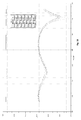
- FIG. 10 is modeled electrical performance for the coupler of FIG. 1 in 3 dB configuration, showing coupling, return loss and port to port isolation between 5.925 and 7.125 Ghz.
- FIG. 11 is modeled electrical performance for the coupler of FIG. 1 in 6 dB configuration, showing coupling, return loss and port to port isolation between 5.925 and 7.125 Ghz.
- the inventors have recognized that the prior waveguide couplers incorporate an excessive number of discrete components and/or surface features with minimal parts harmonization between couplers with different coupling levels.
- An exemplary waveguide coupler as shown in FIGS. 1-9 , has a broad operating frequency band and may be configured for multiple coupling levels via the easy exchange of a single element.
- a trough portion 2 is provided with a first trough 4 and a second trough 6 .
- the first trough 4 and the second trough 6 are each provided with a bottom (removed from FIGS. 1-5 for clarity), an outer sidewall 8 and an inner sidewall 10 ; the inner sidewall 10 of the first trough 4 and the inner sidewall 10 of the second trough 6 are adjacent one another.
- a coupling slot 12 between the inner sidewall(s) 10 communicates between the first trough 4 and the second trough 6 .
- the coupling slot 12 length may be selected according to, for example 1 ⁇ 2 guide wavelength and waveguide geometry.
- An inward projecting abutment 14 may be provided in each outer sidewall 8 , opposite the coupling slot 12 .
- the coupling slot 12 may be provided with a length along a longitudinal axis of the trough portion 2 that is greater than a width of the first trough 4 .
- a cover 16 seats upon an open top 24 of the trough portion 2 to close the first trough 4 and the second trough 6 , forming first and second waveguides 18 , 22 .
- first trough 4 and the second trough 6 may be provided with a plurality of bend(s) 24 operative to locate the inner sidewall(s) 10 proximate the coupling slot 12 close to one another and to space the first and second waveguides 18 , 22 parallel and apart at interconnection end(s) 26 so that suitable spacing is provided for ease of access to selected interconnection means, such as waveguide flanges or the like, for interconnection of the coupler with further waveguides.
- selected interconnection means such as waveguide flanges or the like
- the cover 16 may be provided with protrusion(s) 28 extending into the first trough 4 and the second trough 6 .
- the protrusion(s) 28 may be formed as a stepped ridge with a plurality of step(s) 30 in height. Further, the steps may also be provided with respect to lateral position.
- the step(s) 30 may be dimensioned symmetrically with respect to a center step 32 of the protrusion(s) 28 , for example with a length and width corresponding to 0.25 and 0.05 wavelengths, respectively, of a desired operating frequency, the resulting protrusion(s) 28 binding RF energy as it passes, lowering the level of coupling across the coupling slot 12 .
- the step(s) 30 may be provided with a maximum inward extension from the cover 16 and a minimum lateral distance from the coupling slot 12 proximate a center of the coupling slot 12 selected with respect to desired RF performance, such as coupling, return loss and port to port isolation.
- a height differential between adjacent step(s) 30 may reduce with each step 30 toward the center step 32 .
- a maximum inward extension of the step(s) 30 may be less than half of a height of the first trough 4 .
- two step(s) 30 are provided on each side of the center step 32 .
- the steps in lateral position may be provided with a radius transition 34 between each step 30 .
- the steps in height may be provided with a right angle transition 36 between each step 30 .
- the cover 16 may be provided with a flat surface, for example as shown in FIG. 9 .
- the same trough portion 2 is operable at either a high or low coupling level via simple exchange of the cover 16 .
- the cover 16 attachment to the trough portion 2 for example via a plurality of fasteners or the like (not shown) may be configured to be swappable between a high coupling level flat surface, on a first side (not shown) and a low coupling level surface with the stepped inward projecting protrusions on a second side 38 , eliminating the need for an additional separate part to obtain an easily selectable dual coupling level functionality.
- Modeled electrical performance for the exemplary 3 dB ( FIG. 10 ) and 6 dB ( FIG. 11 ) coupler configurations demonstrates even coupling performance across a wide operating band, with high directivity.
- the trough portion 2 and the cover portion 16 may be cost effectively manufactured with high precision via three axis machining, die casting, metal injection molding and/or a combination of casting/molding followed by machining.
- Specific dimensions of the coupling slot 12 , protrusion(s) 28 and abutment(s) 14 may be selected according to the desired waveguide dimensions, coupling level and operating frequency band. Because of the ability for the coupler to be configured as a 3 dB or 6 dB coupler, prior requirements for design, manufacture and stocking of multiple separate couplers have been eliminated. Further, configuration for use as either a 3 dB or 6 dB coupler may be quickly performed in the field with minimal chance of installation error.
Abstract
Description
| Table of |
| 2 | trough portion |
| 4 | first trough |
| 6 | |
| 8 | |
| 10 | |
| 12 | |
| 14 | |
| 16 | cover |
| 18 | first waveguide |
| 22 | |
| 24 | |
| 26 | |
| 28 | |
| 30 | |
| 32 | |
| 34 | |
| 36 | |
| 38 | second side |
Claims (18)
Priority Applications (6)
| Application Number | Priority Date | Filing Date | Title |
|---|---|---|---|
| US12/901,760 US8324983B2 (en) | 2010-10-11 | 2010-10-11 | Selectable coupling level waveguide coupler |
| CN2011800045717A CN102640349A (en) | 2010-10-11 | 2011-09-08 | Selectable coupling level waveguide coupler |
| CA2780008A CA2780008A1 (en) | 2010-10-11 | 2011-09-08 | Selectable coupling level waveguide coupler |
| PCT/US2011/050764 WO2012050689A1 (en) | 2010-10-11 | 2011-09-08 | Selectable Coupling Level Waveguide Coupler |
| EP11832923.4A EP2494651B1 (en) | 2010-10-11 | 2011-09-08 | Selectable Coupling Level Waveguide Coupler |
| KR1020127012508A KR20130118200A (en) | 2010-10-11 | 2011-09-08 | Selectable coupling level waveguide coupler |
Applications Claiming Priority (1)
| Application Number | Priority Date | Filing Date | Title |
|---|---|---|---|
| US12/901,760 US8324983B2 (en) | 2010-10-11 | 2010-10-11 | Selectable coupling level waveguide coupler |
Publications (2)
| Publication Number | Publication Date |
|---|---|
| US20120086518A1 US20120086518A1 (en) | 2012-04-12 |
| US8324983B2 true US8324983B2 (en) | 2012-12-04 |
Family
ID=45924682
Family Applications (1)
| Application Number | Title | Priority Date | Filing Date |
|---|---|---|---|
| US12/901,760 Active 2031-04-01 US8324983B2 (en) | 2010-10-11 | 2010-10-11 | Selectable coupling level waveguide coupler |
Country Status (6)
| Country | Link |
|---|---|
| US (1) | US8324983B2 (en) |
| EP (1) | EP2494651B1 (en) |
| KR (1) | KR20130118200A (en) |
| CN (1) | CN102640349A (en) |
| CA (1) | CA2780008A1 (en) |
| WO (1) | WO2012050689A1 (en) |
Cited By (2)
| Publication number | Priority date | Publication date | Assignee | Title |
|---|---|---|---|---|
| US20160380331A1 (en) * | 2015-06-24 | 2016-12-29 | Fujikura Ltd. | Directional coupler and diplexer |
| US20160380330A1 (en) * | 2015-06-24 | 2016-12-29 | Fujikura Ltd. | Directional coupler and diplexer |
Families Citing this family (10)
| Publication number | Priority date | Publication date | Assignee | Title |
|---|---|---|---|---|
| CN103107403B (en) * | 2013-03-11 | 2015-07-15 | 成都赛纳赛德科技有限公司 | Loaded power divider |
| CN103151593B (en) * | 2013-03-11 | 2015-09-09 | 成都赛纳赛德科技有限公司 | Novel equiphase power divider |
| CN103682541B (en) * | 2013-11-25 | 2015-08-26 | 中国计量学院 | THz wave one point of four power splitter of unsymmetric structure |
| CN103633404B (en) * | 2013-11-26 | 2015-12-02 | 中国电子科技集团公司第四十一研究所 | A kind of asymmetric ridge-waveguide multipath power distributor and power distribution method |
| US9577323B2 (en) | 2014-03-07 | 2017-02-21 | Commscope Technologies Llc | Radome—reflector assembly mechanism |
| US9612317B2 (en) * | 2014-08-17 | 2017-04-04 | Google Inc. | Beam forming network for feeding short wall slotted waveguide arrays |
| CN104638336A (en) * | 2015-02-16 | 2015-05-20 | 成都赛纳赛德科技有限公司 | Main line segment height change directional coupler |
| CN105789914B (en) * | 2016-04-27 | 2018-08-10 | 安徽四创电子股份有限公司 | Feed structure for Waveguide slot frequency scanning antenna |
| RU2654989C1 (en) * | 2017-05-22 | 2018-05-23 | Акционерное общество Центральное конструкторское бюро аппаратостроения | Waveguide directional coupler |
| JP7186034B2 (en) * | 2018-08-01 | 2022-12-08 | 古野電気株式会社 | Composite distributor |
Citations (26)
| Publication number | Priority date | Publication date | Assignee | Title |
|---|---|---|---|---|
| US2558385A (en) | 1946-01-07 | 1951-06-26 | Edward M Purcell | Branch guide coupler |
| US2626990A (en) | 1948-05-04 | 1953-01-27 | Bell Telephone Labor Inc | Guided wave frequency range transducer |
| FR1115719A (en) | 1953-11-10 | 1956-04-27 | Airtron | Waveguide connections |
| US2951997A (en) | 1957-02-05 | 1960-09-06 | Gen Dynamics Corp | Directional coupler |
| US2975381A (en) | 1957-02-21 | 1961-03-14 | Raytheon Co | Duplexers |
| US3044026A (en) | 1958-05-28 | 1962-07-10 | Gen Electric Co Ltd | Transmission line coupling arrangements |
| DE1192713B (en) | 1962-01-19 | 1965-05-13 | Siemens Ag | Waveguide short-slot directional coupler coupled on the narrow side |
| US3758879A (en) | 1971-08-31 | 1973-09-11 | Int Standard Electric Corp | Variable directional coupler |
| US4146817A (en) | 1977-03-14 | 1979-03-27 | Varian Associates, Inc. | Standing wave linear accelerator and slotted waveguide hybrid junction input coupler |
| US4567401A (en) | 1982-06-12 | 1986-01-28 | The United States Of America As Represented By The Secretary Of The Navy | Wide-band distributed rf coupler |
| US4635006A (en) | 1984-12-18 | 1987-01-06 | Rca Corporation | Adjustable waveguide branch directional coupler |
| US4679011A (en) | 1986-03-21 | 1987-07-07 | Rca Corporation | Waveguide directional coupler family with a common housing having different sets of conductive block insertable therein |
| US4686493A (en) * | 1985-10-02 | 1987-08-11 | Hughes Aircraft Company | Wideband short slot hybrid coupler |
| US4792770A (en) | 1987-06-29 | 1988-12-20 | General Electric Company | Waveguide directional coupler with multiple coupled outputs |
| US4812788A (en) * | 1987-11-02 | 1989-03-14 | Hughes Aircraft Company | Waveguide matrix including in-plane crossover |
| US4818964A (en) | 1986-04-28 | 1989-04-04 | Hughes Aircraft Company | Switchable multi-power-level short slot waveguide hybrid coupler |
| JPH0353007A (en) | 1989-07-19 | 1991-03-07 | Nkk Corp | Manufacture of metal strip |
| US5047738A (en) | 1990-10-09 | 1991-09-10 | Hughes Aircraft Company | Ridged waveguide hybrid |
| US5247268A (en) | 1992-01-06 | 1993-09-21 | General Electric Company | Adjustable waveguide branch, and directional coupler |
| JPH10126118A (en) | 1996-10-16 | 1998-05-15 | Nec Corp | Short slot type directional coupler |
| US6127902A (en) | 1997-04-18 | 2000-10-03 | Robert Bosch Gmbh | Waveguide directional coupler capable of propagating higher order modes |
| US20020093384A1 (en) | 2001-01-12 | 2002-07-18 | Woods Donnie W. | High-directivity and adjusable directional couplers and method therefor |
| US20060284700A1 (en) | 2003-04-25 | 2006-12-21 | Jurek Dabrowski | Directional coupler |
| US20090289742A1 (en) | 2006-03-31 | 2009-11-26 | Nobuhiko Oguma | Waveguide coupler |
| US7671700B1 (en) | 2002-01-23 | 2010-03-02 | Ericsson Ab | Hollow waveguide directional coupler |
| US20100238085A1 (en) | 2009-03-23 | 2010-09-23 | Toyota Motor Engineering & Manufacturing North America, Inc. | Plastic waveguide slot array and method of manufacture |
Family Cites Families (4)
| Publication number | Priority date | Publication date | Assignee | Title |
|---|---|---|---|---|
| GB826788A (en) * | 1957-04-03 | 1960-01-20 | Cole E K Ltd | Improvements in or relating to wave-guides |
| US3535659A (en) * | 1968-03-11 | 1970-10-20 | Edward Salzberg | Waveguide hybrid junctions |
| US4688006A (en) * | 1985-10-02 | 1987-08-18 | Hughes Aircraft Company | Phase compensated hybrid coupler |
| WO2009114731A2 (en) * | 2008-03-13 | 2009-09-17 | Viasat, Inc. | Multi-level power amplification system |
-
2010
- 2010-10-11 US US12/901,760 patent/US8324983B2/en active Active
-
2011
- 2011-09-08 CN CN2011800045717A patent/CN102640349A/en active Pending
- 2011-09-08 EP EP11832923.4A patent/EP2494651B1/en not_active Not-in-force
- 2011-09-08 CA CA2780008A patent/CA2780008A1/en active Pending
- 2011-09-08 KR KR1020127012508A patent/KR20130118200A/en not_active Application Discontinuation
- 2011-09-08 WO PCT/US2011/050764 patent/WO2012050689A1/en active Application Filing
Patent Citations (26)
| Publication number | Priority date | Publication date | Assignee | Title |
|---|---|---|---|---|
| US2558385A (en) | 1946-01-07 | 1951-06-26 | Edward M Purcell | Branch guide coupler |
| US2626990A (en) | 1948-05-04 | 1953-01-27 | Bell Telephone Labor Inc | Guided wave frequency range transducer |
| FR1115719A (en) | 1953-11-10 | 1956-04-27 | Airtron | Waveguide connections |
| US2951997A (en) | 1957-02-05 | 1960-09-06 | Gen Dynamics Corp | Directional coupler |
| US2975381A (en) | 1957-02-21 | 1961-03-14 | Raytheon Co | Duplexers |
| US3044026A (en) | 1958-05-28 | 1962-07-10 | Gen Electric Co Ltd | Transmission line coupling arrangements |
| DE1192713B (en) | 1962-01-19 | 1965-05-13 | Siemens Ag | Waveguide short-slot directional coupler coupled on the narrow side |
| US3758879A (en) | 1971-08-31 | 1973-09-11 | Int Standard Electric Corp | Variable directional coupler |
| US4146817A (en) | 1977-03-14 | 1979-03-27 | Varian Associates, Inc. | Standing wave linear accelerator and slotted waveguide hybrid junction input coupler |
| US4567401A (en) | 1982-06-12 | 1986-01-28 | The United States Of America As Represented By The Secretary Of The Navy | Wide-band distributed rf coupler |
| US4635006A (en) | 1984-12-18 | 1987-01-06 | Rca Corporation | Adjustable waveguide branch directional coupler |
| US4686493A (en) * | 1985-10-02 | 1987-08-11 | Hughes Aircraft Company | Wideband short slot hybrid coupler |
| US4679011A (en) | 1986-03-21 | 1987-07-07 | Rca Corporation | Waveguide directional coupler family with a common housing having different sets of conductive block insertable therein |
| US4818964A (en) | 1986-04-28 | 1989-04-04 | Hughes Aircraft Company | Switchable multi-power-level short slot waveguide hybrid coupler |
| US4792770A (en) | 1987-06-29 | 1988-12-20 | General Electric Company | Waveguide directional coupler with multiple coupled outputs |
| US4812788A (en) * | 1987-11-02 | 1989-03-14 | Hughes Aircraft Company | Waveguide matrix including in-plane crossover |
| JPH0353007A (en) | 1989-07-19 | 1991-03-07 | Nkk Corp | Manufacture of metal strip |
| US5047738A (en) | 1990-10-09 | 1991-09-10 | Hughes Aircraft Company | Ridged waveguide hybrid |
| US5247268A (en) | 1992-01-06 | 1993-09-21 | General Electric Company | Adjustable waveguide branch, and directional coupler |
| JPH10126118A (en) | 1996-10-16 | 1998-05-15 | Nec Corp | Short slot type directional coupler |
| US6127902A (en) | 1997-04-18 | 2000-10-03 | Robert Bosch Gmbh | Waveguide directional coupler capable of propagating higher order modes |
| US20020093384A1 (en) | 2001-01-12 | 2002-07-18 | Woods Donnie W. | High-directivity and adjusable directional couplers and method therefor |
| US7671700B1 (en) | 2002-01-23 | 2010-03-02 | Ericsson Ab | Hollow waveguide directional coupler |
| US20060284700A1 (en) | 2003-04-25 | 2006-12-21 | Jurek Dabrowski | Directional coupler |
| US20090289742A1 (en) | 2006-03-31 | 2009-11-26 | Nobuhiko Oguma | Waveguide coupler |
| US20100238085A1 (en) | 2009-03-23 | 2010-09-23 | Toyota Motor Engineering & Manufacturing North America, Inc. | Plastic waveguide slot array and method of manufacture |
Non-Patent Citations (1)
| Title |
|---|
| Byung IL AN, International Search Report for counterpart application PCT/US2011/050764, Feb. 27, 2012, Korean Intellectual Property Office, Seo-gu, Daejeon, Korea. |
Cited By (4)
| Publication number | Priority date | Publication date | Assignee | Title |
|---|---|---|---|---|
| US20160380331A1 (en) * | 2015-06-24 | 2016-12-29 | Fujikura Ltd. | Directional coupler and diplexer |
| US20160380330A1 (en) * | 2015-06-24 | 2016-12-29 | Fujikura Ltd. | Directional coupler and diplexer |
| US9831897B2 (en) * | 2015-06-24 | 2017-11-28 | Fujikura Ltd. | Directional coupler and diplexer |
| US10135108B2 (en) * | 2015-06-24 | 2018-11-20 | Fujikura Ltd. | Directional coupler and diplexer |
Also Published As
| Publication number | Publication date |
|---|---|
| EP2494651A4 (en) | 2013-04-24 |
| CA2780008A1 (en) | 2012-04-19 |
| CN102640349A (en) | 2012-08-15 |
| WO2012050689A1 (en) | 2012-04-19 |
| US20120086518A1 (en) | 2012-04-12 |
| EP2494651A1 (en) | 2012-09-05 |
| KR20130118200A (en) | 2013-10-29 |
| EP2494651B1 (en) | 2013-12-11 |
Similar Documents
| Publication | Publication Date | Title |
|---|---|---|
| US8324983B2 (en) | Selectable coupling level waveguide coupler | |
| US8698683B2 (en) | Dual polarized reflector antenna assembly | |
| US8222977B2 (en) | Metal plate for preventing radiowave leakage through an aperture in a waveguide body | |
| US6995724B2 (en) | Waveguide slot type radiator having construction to facilitate manufacture | |
| US10164307B2 (en) | Waveguide bend formed in a metal block and coupled to a board unit to form a wireless device | |
| US20170263991A1 (en) | Partial dielectric loaded septum polarizer | |
| CN101317299B (en) | Waveguide bandstop filter | |
| CN114335957B (en) | Power combining/distributing device | |
| CN210272674U (en) | Antenna pair and MIMO antenna system | |
| KR101259702B1 (en) | waveguide power divider | |
| US20160248164A1 (en) | Very compact tm01 mode extractor | |
| CA1259676A (en) | 14/12 ghz duplexer | |
| CN111029704A (en) | Compact waveguide bidirectional coupler | |
| KR101085867B1 (en) | A straight-coupled polarization transition of waveguide and method of designing the same | |
| JP3846585B2 (en) | Waveguide bend, waveguide plate and high frequency device | |
| CN205376723U (en) | Four port networks of compact | |
| CN209747702U (en) | Coupler | |
| CN103050758B (en) | I-type five-port E-surface power divider | |
| CN105811115A (en) | Dielectric substrate integrated dielectric resonator antenna | |
| CN212695294U (en) | Low-profile waveguide series-feed power divider | |
| CN103151592B (en) | H ground roll leads not decile power splitter | |
| CN110800159B (en) | Feed equipment | |
| CN103066366B (en) | Reversed-letter-pi five-port H-face power divider | |
| EP2780978B1 (en) | Antenna adapter | |
| CN112909474A (en) | Double-conductor transmission line directional coupler |
Legal Events
| Date | Code | Title | Description |
|---|---|---|---|
| AS | Assignment |
Owner name: ANDREW LLC, NORTH CAROLINA Free format text: ASSIGNMENT OF ASSIGNORS INTEREST;ASSIGNOR:BRANDAU, RONALD J.;REEL/FRAME:025120/0120 Effective date: 20101011 |
|
| AS | Assignment |
Owner name: JPMORGAN CHASE BANK, N.A., AS COLLATERAL AGENT, NE Free format text: SECURITY AGREEMENT;ASSIGNORS:ALLEN TELECOM LLC, A DELAWARE LLC;ANDREW LLC, A DELAWARE LLC;COMMSCOPE, INC. OF NORTH CAROLINA, A NORTH CAROLINA CORPORATION;REEL/FRAME:026276/0363 Effective date: 20110114 |
|
| AS | Assignment |
Owner name: JPMORGAN CHASE BANK, N.A., AS COLLATERAL AGENT, NE Free format text: SECURITY AGREEMENT;ASSIGNORS:ALLEN TELECOM LLC, A DELAWARE LLC;ANDREW LLC, A DELAWARE LLC;COMMSCOPE, INC OF NORTH CAROLINA, A NORTH CAROLINA CORPORATION;REEL/FRAME:026272/0543 Effective date: 20110114 |
|
| STCF | Information on status: patent grant |
Free format text: PATENTED CASE |
|
| AS | Assignment |
Owner name: COMMSCOPE TECHNOLOGIES LLC, NORTH CAROLINA Free format text: CHANGE OF NAME;ASSIGNOR:ANDREW LLC;REEL/FRAME:035286/0001 Effective date: 20150301 |
|
| AS | Assignment |
Owner name: WILMINGTON TRUST, NATIONAL ASSOCIATION, AS COLLATERAL AGENT, CONNECTICUT Free format text: SECURITY INTEREST;ASSIGNORS:ALLEN TELECOM LLC;COMMSCOPE TECHNOLOGIES LLC;COMMSCOPE, INC. OF NORTH CAROLINA;AND OTHERS;REEL/FRAME:036201/0283 Effective date: 20150611 Owner name: WILMINGTON TRUST, NATIONAL ASSOCIATION, AS COLLATE Free format text: SECURITY INTEREST;ASSIGNORS:ALLEN TELECOM LLC;COMMSCOPE TECHNOLOGIES LLC;COMMSCOPE, INC. OF NORTH CAROLINA;AND OTHERS;REEL/FRAME:036201/0283 Effective date: 20150611 |
|
| FPAY | Fee payment |
Year of fee payment: 4 |
|
| AS | Assignment |
Owner name: COMMSCOPE TECHNOLOGIES LLC, NORTH CAROLINA Free format text: RELEASE OF SECURITY INTEREST PATENTS (RELEASES RF 036201/0283);ASSIGNOR:WILMINGTON TRUST, NATIONAL ASSOCIATION;REEL/FRAME:042126/0434 Effective date: 20170317 Owner name: ALLEN TELECOM LLC, NORTH CAROLINA Free format text: RELEASE OF SECURITY INTEREST PATENTS (RELEASES RF 036201/0283);ASSIGNOR:WILMINGTON TRUST, NATIONAL ASSOCIATION;REEL/FRAME:042126/0434 Effective date: 20170317 Owner name: REDWOOD SYSTEMS, INC., NORTH CAROLINA Free format text: RELEASE OF SECURITY INTEREST PATENTS (RELEASES RF 036201/0283);ASSIGNOR:WILMINGTON TRUST, NATIONAL ASSOCIATION;REEL/FRAME:042126/0434 Effective date: 20170317 Owner name: COMMSCOPE, INC. OF NORTH CAROLINA, NORTH CAROLINA Free format text: RELEASE OF SECURITY INTEREST PATENTS (RELEASES RF 036201/0283);ASSIGNOR:WILMINGTON TRUST, NATIONAL ASSOCIATION;REEL/FRAME:042126/0434 Effective date: 20170317 |
|
| AS | Assignment |
Owner name: ALLEN TELECOM LLC, ILLINOIS Free format text: RELEASE BY SECURED PARTY;ASSIGNOR:JPMORGAN CHASE BANK, N.A.;REEL/FRAME:048840/0001 Effective date: 20190404 Owner name: COMMSCOPE, INC. OF NORTH CAROLINA, NORTH CAROLINA Free format text: RELEASE BY SECURED PARTY;ASSIGNOR:JPMORGAN CHASE BANK, N.A.;REEL/FRAME:048840/0001 Effective date: 20190404 Owner name: ANDREW LLC, NORTH CAROLINA Free format text: RELEASE BY SECURED PARTY;ASSIGNOR:JPMORGAN CHASE BANK, N.A.;REEL/FRAME:048840/0001 Effective date: 20190404 Owner name: COMMSCOPE TECHNOLOGIES LLC, NORTH CAROLINA Free format text: RELEASE BY SECURED PARTY;ASSIGNOR:JPMORGAN CHASE BANK, N.A.;REEL/FRAME:048840/0001 Effective date: 20190404 Owner name: REDWOOD SYSTEMS, INC., NORTH CAROLINA Free format text: RELEASE BY SECURED PARTY;ASSIGNOR:JPMORGAN CHASE BANK, N.A.;REEL/FRAME:048840/0001 Effective date: 20190404 Owner name: COMMSCOPE TECHNOLOGIES LLC, NORTH CAROLINA Free format text: RELEASE BY SECURED PARTY;ASSIGNOR:JPMORGAN CHASE BANK, N.A.;REEL/FRAME:049260/0001 Effective date: 20190404 Owner name: REDWOOD SYSTEMS, INC., NORTH CAROLINA Free format text: RELEASE BY SECURED PARTY;ASSIGNOR:JPMORGAN CHASE BANK, N.A.;REEL/FRAME:049260/0001 Effective date: 20190404 Owner name: COMMSCOPE, INC. OF NORTH CAROLINA, NORTH CAROLINA Free format text: RELEASE BY SECURED PARTY;ASSIGNOR:JPMORGAN CHASE BANK, N.A.;REEL/FRAME:049260/0001 Effective date: 20190404 Owner name: ALLEN TELECOM LLC, ILLINOIS Free format text: RELEASE BY SECURED PARTY;ASSIGNOR:JPMORGAN CHASE BANK, N.A.;REEL/FRAME:049260/0001 Effective date: 20190404 Owner name: ANDREW LLC, NORTH CAROLINA Free format text: RELEASE BY SECURED PARTY;ASSIGNOR:JPMORGAN CHASE BANK, N.A.;REEL/FRAME:049260/0001 Effective date: 20190404 |
|
| AS | Assignment |
Owner name: JPMORGAN CHASE BANK, N.A., NEW YORK Free format text: TERM LOAN SECURITY AGREEMENT;ASSIGNORS:COMMSCOPE, INC. OF NORTH CAROLINA;COMMSCOPE TECHNOLOGIES LLC;ARRIS ENTERPRISES LLC;AND OTHERS;REEL/FRAME:049905/0504 Effective date: 20190404 Owner name: JPMORGAN CHASE BANK, N.A., NEW YORK Free format text: ABL SECURITY AGREEMENT;ASSIGNORS:COMMSCOPE, INC. OF NORTH CAROLINA;COMMSCOPE TECHNOLOGIES LLC;ARRIS ENTERPRISES LLC;AND OTHERS;REEL/FRAME:049892/0396 Effective date: 20190404 Owner name: WILMINGTON TRUST, NATIONAL ASSOCIATION, AS COLLATE Free format text: PATENT SECURITY AGREEMENT;ASSIGNOR:COMMSCOPE TECHNOLOGIES LLC;REEL/FRAME:049892/0051 Effective date: 20190404 Owner name: WILMINGTON TRUST, NATIONAL ASSOCIATION, AS COLLATERAL AGENT, CONNECTICUT Free format text: PATENT SECURITY AGREEMENT;ASSIGNOR:COMMSCOPE TECHNOLOGIES LLC;REEL/FRAME:049892/0051 Effective date: 20190404 |
|
| MAFP | Maintenance fee payment |
Free format text: PAYMENT OF MAINTENANCE FEE, 8TH YEAR, LARGE ENTITY (ORIGINAL EVENT CODE: M1552); ENTITY STATUS OF PATENT OWNER: LARGE ENTITY Year of fee payment: 8 |
|
| AS | Assignment |
Owner name: WILMINGTON TRUST, DELAWARE Free format text: SECURITY INTEREST;ASSIGNORS:ARRIS SOLUTIONS, INC.;ARRIS ENTERPRISES LLC;COMMSCOPE TECHNOLOGIES LLC;AND OTHERS;REEL/FRAME:060752/0001 Effective date: 20211115 |