US8325647B2 - Time-division multiplexer and signal transmission apparatus - Google Patents
Time-division multiplexer and signal transmission apparatus Download PDFInfo
- Publication number
- US8325647B2 US8325647B2 US12/750,232 US75023210A US8325647B2 US 8325647 B2 US8325647 B2 US 8325647B2 US 75023210 A US75023210 A US 75023210A US 8325647 B2 US8325647 B2 US 8325647B2
- Authority
- US
- United States
- Prior art keywords
- output
- group
- input signals
- signal
- clock
- Prior art date
- Legal status (The legal status is an assumption and is not a legal conclusion. Google has not performed a legal analysis and makes no representation as to the accuracy of the status listed.)
- Active, expires
Links
Images


Classifications
-
- H—ELECTRICITY
- H04—ELECTRIC COMMUNICATION TECHNIQUE
- H04J—MULTIPLEX COMMUNICATION
- H04J3/00—Time-division multiplex systems
- H04J3/02—Details
- H04J3/04—Distributors combined with modulators or demodulators
- H04J3/047—Distributors with transistors or integrated circuits
-
- H—ELECTRICITY
- H04—ELECTRIC COMMUNICATION TECHNIQUE
- H04L—TRANSMISSION OF DIGITAL INFORMATION, e.g. TELEGRAPHIC COMMUNICATION
- H04L7/00—Arrangements for synchronising receiver with transmitter
- H04L7/0008—Synchronisation information channels, e.g. clock distribution lines
Definitions
- the technology disclosed in this specification relates to time-division multiplexers which multiplex a plurality of signals in a time-division multiplexed manner, and to signal transmission devices including the same.
- Patent Document 1 Japanese Unexamined Patent Application Publication No. 2003-8995 discloses a drive unit for transferring CCD charge which includes a time-division multiplexer and a demultiplexer.
- This drive unit for transferring CCD charge includes a timing signal generator which provides a plurality of timing signals (a plurality of timing signals for read pulses and a plurality of timing signals for vertical transfer), and a vertical driver which outputs a plurality of vertical drive pulses for driving a vertical transfer section of a solid-state imaging device (e.g., a CCD image sensor, etc.) according to the plurality of timing signals from the timing signal generator.
- the time-division multiplexer and the demultiplexer are respectively provided in the timing signal generator and the vertical driver.
- the time-division multiplexer multiplexes, in a time division multiplexed manner, combinations of the plurality of timing signals for read pulses and the plurality of timing signals for vertical transfer, and generates a plurality of multiplexed signals, while the demultiplexer demultiplexes the plurality of multiplexed signals into respective combinations of a plurality of timing signals for read pulses and a plurality of timing signals for vertical transfer.
- the time-division multiplexer of Patent Document 1 is subject to restrictions on a timing relationship between signal transitions of input signals to be multiplexed. Specifically, upon time-division multiplexing of two input signals, if the signal level of one input signal transitions while the other input signal has been selected as a signal to be multiplexed therewith, the two input signals cannot be properly multiplexed. Thus, only input signals having a particular relationship (e.g., timing signals for read pulses and timing signals for vertical transfer) can be multiplexed, making it difficult to improve a reducing effect, due to time-division multiplexing, on the number of signal lines (i.e., the number of terminals in a circuit).
- timing signals for read pulses and timing signals for vertical transfer can be multiplexed, making it difficult to improve a reducing effect, due to time-division multiplexing, on the number of signal lines (i.e., the number of terminals in a circuit).
- the number of lines of timing signals for read pulses is generally less than the number of lines of timing signals for vertical transfer.
- the number of lines of timing signals which can be multiplexed is limited by the number of lines of timing signals for read pulses, making it difficult to improve a reducing effect on the number of signal lines.
- a time-division multiplexer is a circuit which multiplexes respective combinations of n (where n is an integer more than 1) first input signals and n second input signals to generate n multiplexed signals; and includes n signal transition detection sections corresponding to respective combinations of the n first input signals and the n second input signals, and each configured to detect a transition of the signal level of at least one of the first or the second input signal of the combination corresponding thereto, a time-division control section configured to output a control pulse according to a system clock when a signal transition is detected by at least one of the n signal transition detection sections, and n output switching sections corresponding to respective combinations of the n first input signals and the n second input signals, and each configured to output either the first or the second input signal of the combination corresponding thereto as one of the multiplexed signals according to the control pulse.
- the aforementioned time-division multiplexer is capable of relaxing restrictions on a timing relationship between signal transitions of the input signals
- control pulse may include two types of control pulses, one of which is a first control pulse output in synchronization with the system clock, and the other of which is a second control pulse output after the first control pulse; and the n output switching sections may each output the first input signal corresponding thereto as the one of the multiplexed signals in a period during which the first control pulse is output, and output the second input signal corresponding thereto as the one of the multiplexed signals in a period during which the second control pulse is output.
- the time-division multiplexer may further include a timing generation section; the time-division control section may output a permit pulse and the control pulse according to the system clock when a signal transition is detected by at least one of the n signal transition detection sections; the timing generation section may output a frequency-multiplied clock having a higher frequency than that of the system clock as a timing clock in a period during which the permit pulse is output; and the n output switching sections may each include a selector configured to select the first input signal corresponding to the output switching section in a period during which the control pulse is not output, and to select the second input signal corresponding to the output switching section in a period during which the control pulse is output, and a flip-flop configured to load the input signal selected by the selector in synchronization with the timing clock, and to output the loaded signal as the one of the multiplexed signals.
- a glitch or a hazard occurred in the time-division multiplexer can be prevented from affecting the demultiplexer.
- the time-division multiplexer may further include a decode-clock generation section; the time-division control section may output a permit pulse and the one or more control pulses according to the system clock when a signal transition is detected by at least one of the n signal transition detection sections; the decode-clock generation section may generate a decode clock used for demultiplexing the n multiplexed signals according to definition clocks corresponding to the system clock in a period during which the permit pulse is output.
- the time-division multiplexer may further include a clock generation section configured to adjust the phase of the system clock and to output the resultant clocks as the definition clocks.
- a clock generation section configured to adjust the phase of the system clock and to output the resultant clocks as the definition clocks.
- Use of such a configuration allows the phase of the decode clock generated in the decode-clock generation section to be adjusted.
- the amount of phase adjustment of the decode clock may be determined considering wiring patterns on the package substrates and delay times due to inter-chip connections.
- FIG. 1 is a diagram illustrating an example configuration of a signal transmission device according to the first embodiment.
- FIG. 2 is a diagram illustrating an example configuration of a signal transition detection section shown in FIG. 1 .
- FIG. 3 is a diagram illustrating an example configuration of the time-division control section shown in FIG. 1 .
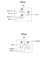
- FIG. 4 is a diagram illustrating an example configuration of an output switching section shown in FIG. 1 .
- FIG. 5 is a diagram illustrating an example configuration of the decode-clock generation section shown in FIG. 1 .
- FIG. 6 is a diagram for illustrating an operation of the multiplexer shown in FIG. 1 .
- FIG. 7 is a diagram for illustrating another operation of the multiplexer shown in FIG. 1 .
- FIG. 8 is a diagram illustrating an example configuration of the decoder shown in FIG. 1 .
- FIG. 9 is a diagram for illustrating an operation of the demultiplexer shown in FIG. 1 .
- FIG. 10 is a diagram for illustrating another operation of the demultiplexer shown in FIG. 1 .
- FIG. 11 is a diagram illustrating an example configuration of a multiplexer according to the second embodiment.
- FIG. 12 is a diagram for illustrating an operation of the multiplexer shown in FIG. 11 .
- FIG. 13 is a diagram for illustrating a variation of the multiplexer shown in FIG. 11 .
- FIG. 14 is a diagram for illustrating an operation of the multiplexer shown in FIG. 13 .
- FIG. 1 illustrates an example configuration of a signal transmission device according to the first embodiment.
- the signal transmission device includes a time-division multiplexer 1 , which multiplexes respective combinations of n (where n is an integer more than 1) first input signals A 1 in, A 2 in, . . . , and Anin, and n second input signals B 1 in, B 2 in, . . . , and Bnin to generate n multiplexed signals C 1 , C 2 , . . . , and Cn, and a demultiplexer 2 , which demultiplexes the n multiplexed signals C 1 , C 2 , . . . , and Cn into combinations of n first output signals A 1 out, A 2 out, . . . , and Anout, and n second output signals B 1 out, B 2 out, . . . , and Bnout.
- n is an integer more than 1
- the time-division multiplexer 1 includes a clock generation section 10 , n signal transition detection sections 111 , 112 , . . . , and 11 n , a time-division control section 12 , n output switching sections 131 , 132 , . . . , and 13 n , and a decode-clock generation section 14 .
- the demultiplexer 2 includes n decoders 151 , 152 , . . . , and 15 n.
- the clock generation section 10 adjusts the phase of a system clock CLKP, and outputs a phase-adjusted system clock as definition clocks (in this case, a rising-edge definition clock CLKR to define a rising edge of a decode clock DCLK, and a falling-edge definition clock CLKF to define a falling edge of the decode clock DCLK).
- a rising-edge definition clock CLKR to define a rising edge of a decode clock DCLK
- a falling-edge definition clock CLKF to define a falling edge of the decode clock DCLK.
- the clock generation section 10 generates the rising-edge definition clock CLKR by delaying the system clock CLKP by a predetermined delay time (e.g., a half-period of the system clock CLKP), and generates the falling-edge definition clock CLKF by inverting the rising-edge definition clock CLKR.
- the n signal transition detection sections 111 , 112 , . . . , and 11 n correspond to respective combinations of the n first input signals A 1 in, A 2 in, . . . , and Anin, and the n second input signals B 1 in, B 2 in, . . . , and Bnin, and output detection pulses Sd 1 , Sd 2 , . . . , and Sdn when detecting a transition of the signal level of at least one of the first or the second input signal of the combination corresponding thereto.
- the time-division control section 12 outputs control pulses (in this case, control pulses Sa and Sb) and a permit pulse Se according to the system clock CLKP when a signal transition is detected by at least one of the signal transition detection sections 111 , 112 , . . . , and 11 n (i.e., at least one of the detection pulses Sd 1 , Sd 2 , . . . , or Sdn is output).
- control pulses in this case, control pulses Sa and Sb
- a permit pulse Se according to the system clock CLKP
- the n output switching sections 131 , 132 , . . . , and 13 n correspond to respective combinations of the n first input signals A 1 in, A 2 in, . . . , and Anin, and the n second input signals B 1 in, B 2 in, . . . , and Bnin, and each outputs either the first or the second input signal of the combination corresponding thereto as one of the multiplexed signals C 1 , C 2 , . . . , and Cn according to the control pulses (in this case, the control pulses Sa and Sb).
- the decode-clock generation section 14 generates a decode clock DCLK according to the definition clocks (in this case, the rising-edge definition clock CLKR and the falling-edge definition clock CLKF) in a period during which the permit pulse Se is output (e.g., a period during which the permit pulse Se is at a high level).
- FIG. 2 illustrates an example configuration of the signal transition detection section 111 shown in FIG. 1 .
- the signal transition detection section 111 includes flip-flops 101 and 102 , XOR circuits 103 and 104 , and an OR circuit 105 .
- the flip-flops 101 and 102 respectively load the first and the second input signals A 1 in and B 1 in in synchronization with a rising edge of the system clock CLKP.
- the XOR circuit 103 outputs a result of a logical exclusive-OR between the first input signal A 1 in and the normal (non-inverted) output signal of the flip-flop 101 , while the XOR circuit 104 outputs a result of a logical exclusive-OR between the second input signal B 1 in and the normal output signal of the flip-flop 102 .
- the OR circuit 105 outputs a result of a logical OR of the outputs of the XOR circuits 103 and 104 as the detection pulse Sd 1 .
- the normal output signal of the flip-flop 101 is at a low level
- the output of the XOR circuit 103 transitions to a high level
- the output of the OR circuit 105 also transitions to a high level.
- the normal output signal of the flip-flop 101 transitions from low to high
- the output of the XOR circuit 103 and the output of the OR circuit 105 transition from high to low.
- FIG. 3 illustrates an example configuration of the time-division control section 12 shown in FIG. 1 .
- the time-division control section 12 includes an OR circuit 201 , an inverter 202 , and flip-flops 203 , 204 , 205 , 206 , and 207 .
- the OR circuit 201 outputs a result of a logical OR of the detection pulses Sd 1 , Sd 2 , . . . , and Sdn.
- the inverter 202 inverts the system clock CLKP, and outputs the result as an inverted clock CLKN.
- the flip-flop 203 loads the output of the OR circuit 201 in synchronization with a rising edge of the system clock CLKP.
- the normal output signal of the flip-flop 203 is output as the control pulse Sa.
- the flip-flop 204 loads the normal output signal of the flip-flop 203 (the control pulse Sa) in synchronization with a rising edge of the inverted clock CLKN.
- the inverted output signal of the flip-flop 204 is applied to the reset terminal of the flip-flop 203 .
- the flip-flop 205 loads the output of the OR circuit 201 in synchronization with a rising edge of the system clock CLKP.
- the normal output signal of the flip-flop 205 is output as the permit pulse Se.
- the flip-flop 206 loads the normal output signal of the flip-flop 205 (the permit pulse Se) in synchronization with a rising edge of the inverted clock CLKN.
- the normal output signal of the flip-flop 206 is output as the control pulse Sb.
- the flip-flop 207 loads the output of the normal output signal of the flip-flop 206 (the control pulse Sb) in synchronization with a rising edge of the system clock CLKP.
- the inverted output signal of the flip-flop 207 is applied to the reset terminal of the flip-flop 206 .
- the normal output signal of the flip-flop 203 transitions from low to high in synchronization with a rising edge of the system clock CLKP. Then, the inverted output signal of the flip-flop 204 transitions from high to low in synchronization with a rising edge of the inverted clock CLKN, and thus, the flip-flop 203 is reset. This causes the normal output signal of the flip-flop 203 (the control pulse Sa) to transition from high to low.
- the normal output signal of the flip-flop 205 transitions from low to high in synchronization with a rising edge of the system clock CLKP.
- the normal output signal of the flip-flop 206 transitions from low to high in synchronization with a rising edge of the inverted clock CLKN.
- the inverted output signal of the flip-flop 207 transitions from high to low in synchronization with a rising edge of the system clock CLKP, and thus, the flip-flop 206 is reset. This causes the normal output signal of the flip-flop 206 (the control pulse Sb) to transition from high to low.
- FIG. 4 illustrates an example configuration of the output switching section 131 shown in FIG. 1 .
- the output switching section 131 includes NAND circuits 301 , 302 , and 303 .
- the NAND circuit 301 outputs a result of a logical NAND between the first input signal A 1 in and the control pulse Sa; the NAND circuit 302 outputs a result of a logical NAND between the second input signal B 1 in and the control pulse Sb; and the NAND circuit 303 outputs a result of a logical NAND between the outputs of the NAND circuits 301 and 302 .
- the first input signal A 1 in is output as the multiplexed signal C 1 in a period during which the control pulse Sa is at a high level
- the second input signal B 1 in is output as the multiplexed signal C 1 in a period during which the control pulse Sb is at a high level.
- FIG. 5 illustrates an example configuration of the decode-clock generation section 14 shown in FIG. 1 .
- the decode-clock generation section 14 includes flip-flops 401 and 402 .
- the flip-flop 401 loads the permit pulse Se in synchronization with a rising edge of the rising-edge definition clock CLKR.
- the normal output signal of the flip-flop 401 is output as the decode clock DCLK.
- the flip-flop 402 loads the normal output signal of the flip-flop 401 (the decode clock DCLK) in synchronization with a rising edge of the falling-edge definition clock CLKF.
- the inverted output signal of the flip-flop 402 is applied to the reset terminal of the flip-flop 401 .
- the normal output signal of the flip-flop 401 transitions from low to high in synchronization with a rising edge of the rising-edge definition clock CLKR. Then, the inverted output signal of the flip-flop 402 transitions from high to low in synchronization with a rising edge of the falling-edge definition clock CLKF, and thus, the flip-flop 401 is reset. This causes the normal output signal of the flip-flop 401 (the decode clock DCLK) to transition from high to low.
- the signal transition detection section 111 drives, at time t 1 , the detection pulse Sd 1 to the high level according to a signal transition of the first input signal A 1 in.
- the time-division control section 12 drives the control pulse Sa and the permit pulse Se to the high level in synchronization with a rising edge of the system clock CLKP. This causes the output switching section 131 to output the first input signal A 1 in as the multiplexed signal C 1 (i.e., the multiplexed signal C 1 is driven to the high level). Then, when a half-period of the system clock CLKP has elapsed after the control pulse Sa and the permit pulse Se were driven to the high level, the time-division control section 12 drives the control pulse Sa to the low level, and the control pulse Sb to the high level.
- the time-division control section 12 drives the permit pulse Se and the control pulse Sb to the low level. This causes the output switching section 131 to stop outputting the multiplexed signal C 1 (i.e., the multiplexed signal C 1 is driven to the low level).
- the signal transition detection section 111 outputs the detection pulse Sd 1 according to a signal transition of the second input signal B 1 in. Then, operation similar to that in the period from t 1 to t 4 is performed in the period from t 5 to t 8 .
- the first input signal A 1 in is output as the multiplexed signal C 1 (i.e., the multiplexed signal C 1 is driven to the high level) in a period during which the control pulse Sa is at a high level
- the second input signal B 1 in is output as the multiplexed signal C 1 (i.e., the multiplexed signal C 1 is driven to the high level) in a period during which the control pulse Sb is at a high level.
- the decode-clock generation section 14 generates the decode clock DCLK according to the rising-edge definition clock CLKR and the falling-edge definition clock CLKF in a period during which the permit pulse Se is at the high level (the period from t 2 to t 3 , and the period from t 6 to t 7 ), and stops generating the decode clock DCLK in a period during which the permit pulse Se is at the low level.
- the signal transition detection section 111 outputs, at time t 9 , the detection pulse Sd 1 according to the signal transitions of the first and the second input signals A 1 in and B 1 in. Then, operation similar to that in the period from t 1 to t 4 of FIG. 6 is performed in the period from t 9 to t 12 .
- the first and the second input signals can be time-division multiplexed in one period of the system clock CLKP.
- the demultiplexer 2 includes n decoders 151 , 152 , . . . , and 15 n .
- the n decoders 151 , 152 , . . . , and 15 n respectively, correspond to the n multiplexed signals C 1 , C 2 , . . . , and Cn, and demultiplexes the multiplexed signals C 1 , C 2 , . . . , and Cn into combinations of first output signals A 1 out, A 2 out, . . . , and Anout, and second output signals B 1 out, B 2 out, . . .
- the decoder 151 loads the multiplexed signal C 1 in synchronization with each of a rising edge and a falling edge of the decode clock DCLK, and outputs the multiplexed signal C 1 loaded in synchronization with a rising edge of the decode clock DCLK as the first output signal A 1 out, and outputs the multiplexed signal C 1 loaded in synchronization with a falling edge of the decode clock DCLK as the second output signal B 1 out.
- FIG. 8 illustrates an example configuration of the decoder 151 shown in FIG. 1 .
- the decoder 151 includes flip-flops 501 , 503 , and 504 , and an inverter 502 .
- the flip-flop 501 loads the multiplexed signal C 1 in synchronization with a rising edge of the decode clock DCLK.
- the inverter 502 inverts the decode clock DCLK.
- the flip-flop 503 loads the normal output signal of the flip-flop 501 in synchronization with a rising edge of the output of the inverter 502 (i.e., a falling edge of the decode clock DCLK).
- the normal output signal of the flip-flop 503 is output as the first output signal A 1 out.
- the flip-flop 504 loads the multiplexed signal C 1 in synchronization with a rising edge of the output of the inverter 502 .
- the normal output signal of the flip-flop 504 is output as the second output signal B 1 out.
- a rising edge and a falling edge of the decode clock DCLK correspond, respectively, to the high level and the low level of the multiplexed signal C 1 in the period from t 2 to t 3 . Therefore, the decoder 151 drives the first output signal A 1 out to the high level and the second output signal B 1 out to the low level in synchronization with a falling edge of the decode clock DCLK. In the period from t 6 to t 7 , a rising edge and a falling edge of the decode clock DCLK both correspond to the high level of the multiplexed signal C 1 . Therefore, the decoder 151 drives both the first and the second output signals A 1 out and B 1 out to the high level in synchronization with a falling edge of the decode clock DCLK.
- the decoder 151 drives both the first and the second output signals A 1 out and B 1 out to the high level in synchronization with a falling edge of the decode clock DCLK.
- a corresponding multiplexed signal can be demultiplexed into a first output signal corresponding to the first input signal, and a second output signal corresponding to the second input signal.
- time-division multiplexer 1 since restrictions on a timing relationship between signal transitions of the input signals to be multiplexed can be relaxed, flexibility in time-division multiplexing can be improved. This allows for improvement on a reducing effect, due to time-division multiplexing, on the number of signal lines (i.e., the number of terminals in the time-division multiplexer 1 , and the number of terminals in the demultiplexer 2 ). In addition, since multiplexing operation is performed only when the signal level of an input signal transitions, current consumption of the time-division multiplexer 1 can be prevented from increasing.
- the clock generation section 10 adjusts the phase of the system clock CLKP, and outputs the resultant clocks as the definition clocks, the phase of the decode clock DCLK generated by the decode-clock generation section 14 can be adjusted.
- the amount of phase adjustment of the decode clock DCLK may be determined considering wiring patterns on the package substrates and delay times due to inter-chip connections. Note that if the definition clocks (i.e., the rising-edge definition clock CLKR and the falling-edge definition clock CLKF) are supplied from the outside of the time-division multiplexer 1 to the decode-clock generation section 14 , the time-division multiplexer 1 does not need to include the clock generation section 10 .
- a signal transmission device includes a time-division multiplexer 3 shown in FIG. 11 and the demultiplexer 2 shown in FIG. 1 .
- the time-division multiplexer 3 shown in FIG. 11 includes n selectors 311 , 312 , . . . , and 31 n instead of the output switching sections 131 , 132 , . . . , and 13 n shown in FIG. 1 .
- the time-division control section 12 provides the control pulse (in this case, the control pulse Sb) to each of the selectors 311 , 312 , . . . , and 31 n .
- the other part of the configuration is similar to the corresponding part of the configuration of the time-division multiplexer 1 shown in FIG. 1 .
- the selectors 311 , 312 , . . . , and 31 n respectively select the first input signals A 1 in, A 2 in, . . . , and Anin as the multiplexed signals C 1 , C 2 , . . . , and Cn in a period during which the control pulse Sb is not output, and respectively select the second input signals B 1 in, B 2 in, . . . , and Bnin as the multiplexed signals C 1 , C 2 , . . . , and Cn in a period during which the control pulse Sb is output.
- the selector 311 generates the multiplexed signal C 1 from the first and the second input signals A 1 in and B 1 in according to whether the control pulse Sb is or is not output.
- the decoder 151 outputs the multiplexed signal C 1 loaded in synchronization with a rising edge of the decode clock DCLK as the first output signal A 1 out, and outputs the multiplexed signal C 1 loaded in synchronization with a falling edge of the decode clock DCLK as the second output signal B 1 out.
- the output switching sections 131 , 132 , . . . , and 13 n of FIG. 1 are respectively replaced with the selectors 311 , 312 , . . . , and 31 n , similarly to the first embodiment, restrictions on a timing relationship between signal transitions of the input signals to be multiplexed can be relaxed.
- FIG. 13 illustrates a variation of the time-division multiplexer shown in FIG. 11 .
- the time-division multiplexer 3 a shown in FIG. 13 further includes, in addition to the components of the time-division multiplexer 3 shown in FIG. 11 , a timing generation section 30 and n flip-flops 321 , 322 , . . . , and 32 n .
- the timing generation section 30 generates a frequency-multiplied clock having a higher frequency than that of the system clock CLKP based on the system clock CLKP (in this case, a frequency-multiplied clock having a frequency which is twice that of the system clock CLKP), and outputs the frequency-multiplied clock as a timing clock TCLK in a period during which the permit pulse Se is output.
- the n selectors 311 , 312 , . . . , and 31 n respectively select and output the first input signals A 1 in, A 2 in, . . . , and Anin as selected signals S 311 , S 312 , . . .
- the n flip-flops 321 , 322 , . . . , and 32 n respectively, correspond to the n selectors 311 , 312 , . . . , and 31 n , load the selected signals S 311 , S 312 , . . .
- the selector 311 generates the selected signal S 311 from the first and the second input signals A 1 in and B 1 in according to whether the control pulse Sb is or is not output.
- the flip-flop 321 loads the selected signal S 311 in synchronization with a rising edge of the timing clock TCLK, and outputs the selected signal S 311 as the multiplexed signal C 1 .
- the time-division multiplexer and the demultiplexer of each example embodiment described previously are applicable to a drive unit for solid-state imaging devices for driving a solid-state imaging device (e.g., a CCD image sensor, etc.).
- the drive unit for solid-state imaging devices includes a timing signal generator which provides a plurality of timing signals (a plurality of timing signals for read pulses and a plurality of timing signals for vertical transfer), and a vertical driver which outputs a plurality of vertical drive pulses for driving a vertical transfer section of a solid-state imaging device according to the plurality of timing signals from the timing signal generator.
- time-division multiplexer 1 (or the time-division multiplexer 3 or 3 a ) in the timing signal generator, and by providing the demultiplexer 2 in the vertical driver, not only combinations of the timing signals for read pulses and the timing signals for vertical transfer, but also combinations of the timing signals for read pulses, the timing signals for vertical transfer, and other signals can be multiplexed. This allows the numbers of terminals of a vertical driver and a timing signal generator to be reduced, thereby allowing the circuit size of a drive unit for solid-state imaging devices to be reduced.
- time-division multiplexers are capable of relaxing restrictions on a timing relationship between signal transitions of input signals to be multiplexed, thus are useful for signal transmission devices, etc.
Abstract
Description
Claims (7)
Applications Claiming Priority (2)
| Application Number | Priority Date | Filing Date | Title |
|---|---|---|---|
| JP2009-086307 | 2009-03-31 | ||
| JP2009086307A JP4791559B2 (en) | 2009-03-31 | 2009-03-31 | Time division multiplexing circuit, signal transmission device |
Publications (2)
| Publication Number | Publication Date |
|---|---|
| US20100246607A1 US20100246607A1 (en) | 2010-09-30 |
| US8325647B2 true US8325647B2 (en) | 2012-12-04 |
Family
ID=42784184
Family Applications (1)
| Application Number | Title | Priority Date | Filing Date |
|---|---|---|---|
| US12/750,232 Active 2031-01-17 US8325647B2 (en) | 2009-03-31 | 2010-03-30 | Time-division multiplexer and signal transmission apparatus |
Country Status (2)
| Country | Link |
|---|---|
| US (1) | US8325647B2 (en) |
| JP (1) | JP4791559B2 (en) |
Families Citing this family (3)
| Publication number | Priority date | Publication date | Assignee | Title |
|---|---|---|---|---|
| EP3028194A2 (en) * | 2013-07-30 | 2016-06-08 | ESS Technology, Inc. | System and method for series and parallel combinations of electrical elements |
| JP2016100674A (en) * | 2014-11-19 | 2016-05-30 | 富士通株式会社 | Transmission device |
| JP2022145009A (en) * | 2021-03-19 | 2022-10-03 | キオクシア株式会社 | Semiconductor integrated circuit and analog-to-digital converter |
Citations (4)
| Publication number | Priority date | Publication date | Assignee | Title |
|---|---|---|---|---|
| US4498167A (en) | 1982-03-01 | 1985-02-05 | International Telephone And Telegraph Corporation | TDM Communication system |
| US5615126A (en) | 1994-08-24 | 1997-03-25 | Lsi Logic Corporation | High-speed internal interconnection technique for integrated circuits that reduces the number of signal lines through multiplexing |
| JP2002064753A (en) | 2000-08-16 | 2002-02-28 | Fuji Film Microdevices Co Ltd | Drive circuit for ccd charge transfer |
| JP2003008995A (en) | 2001-06-22 | 2003-01-10 | Fuji Photo Film Co Ltd | Driver for transferring ccd electric charge |
Family Cites Families (1)
| Publication number | Priority date | Publication date | Assignee | Title |
|---|---|---|---|---|
| JP2000307561A (en) * | 1999-04-21 | 2000-11-02 | Hitachi Ltd | Bus system unit |
-
2009
- 2009-03-31 JP JP2009086307A patent/JP4791559B2/en active Active
-
2010
- 2010-03-30 US US12/750,232 patent/US8325647B2/en active Active
Patent Citations (6)
| Publication number | Priority date | Publication date | Assignee | Title |
|---|---|---|---|---|
| US4498167A (en) | 1982-03-01 | 1985-02-05 | International Telephone And Telegraph Corporation | TDM Communication system |
| US5615126A (en) | 1994-08-24 | 1997-03-25 | Lsi Logic Corporation | High-speed internal interconnection technique for integrated circuits that reduces the number of signal lines through multiplexing |
| US5898677A (en) | 1994-08-24 | 1999-04-27 | Lsi Logic Corporation | Integrated circuit device having a switched routing network |
| JP2002064753A (en) | 2000-08-16 | 2002-02-28 | Fuji Film Microdevices Co Ltd | Drive circuit for ccd charge transfer |
| JP2003008995A (en) | 2001-06-22 | 2003-01-10 | Fuji Photo Film Co Ltd | Driver for transferring ccd electric charge |
| US7053950B2 (en) | 2001-06-22 | 2006-05-30 | Fuji Photo Film Co., Ltd. | Drive unit for transferring CCD charge |
Also Published As
| Publication number | Publication date |
|---|---|
| JP4791559B2 (en) | 2011-10-12 |
| US20100246607A1 (en) | 2010-09-30 |
| JP2010239471A (en) | 2010-10-21 |
Similar Documents
| Publication | Publication Date | Title |
|---|---|---|
| US6750692B2 (en) | Circuit and method for generating internal clock signal | |
| US7777536B2 (en) | Synchronization circuit | |
| US5808571A (en) | Synchronization control unit which maintains synchronization between serial-to-parallel converters operating in parallel, or between parallel-to-serial converters operating in parallel | |
| US20120063557A1 (en) | Phase adjustment circuit, receiving apparatus and communication system | |
| US8325647B2 (en) | Time-division multiplexer and signal transmission apparatus | |
| JP2008508834A (en) | Data transmission synchronization | |
| US7990295B2 (en) | Data transfer apparatus | |
| US20110284727A1 (en) | Ccd charge transfer drive device | |
| KR102140117B1 (en) | Circuit for adjusting clock phase and semiconductor device including the same | |
| US8773188B2 (en) | Switching clock sources | |
| JP2003263238A (en) | Clock generation circuit | |
| KR950019570A (en) | Frame phase aligner | |
| US7616708B2 (en) | Clock recovery circuit | |
| KR101046730B1 (en) | Semiconductor memory device and driving method thereof | |
| JP7059536B2 (en) | Signal transmission circuit | |
| JP2009169981A (en) | Semiconductor device and clock transmission method | |
| US9647650B2 (en) | Clock generating device | |
| KR20090101053A (en) | Apparatus and method for transmitting data with clock information | |
| JP2019047208A (en) | Semiconductor circuit | |
| JP5378765B2 (en) | Data transfer system | |
| US9246616B2 (en) | Clock phase compensator for multi-stage time division multiplexer | |
| JP5286686B2 (en) | Clock transfer circuit | |
| KR100656444B1 (en) | Circuit for outputting data in semiconductor memory apparatus | |
| JP5682458B2 (en) | Data transmission / reception system | |
| US6801055B1 (en) | Data driven clocking |
Legal Events
| Date | Code | Title | Description |
|---|---|---|---|
| AS | Assignment |
Owner name: PANASONIC CORPORATION, JAPAN Free format text: ASSIGNMENT OF ASSIGNORS INTEREST;ASSIGNORS:KAWAJIRI, MAKOTO;KINUGASA, NORIHIDE;HATANI, NAOHISA;REEL/FRAME:025597/0196 Effective date: 20100316 |
|
| FEPP | Fee payment procedure |
Free format text: PAYOR NUMBER ASSIGNED (ORIGINAL EVENT CODE: ASPN); ENTITY STATUS OF PATENT OWNER: LARGE ENTITY |
|
| STCF | Information on status: patent grant |
Free format text: PATENTED CASE |
|
| FEPP | Fee payment procedure |
Free format text: PAYER NUMBER DE-ASSIGNED (ORIGINAL EVENT CODE: RMPN); ENTITY STATUS OF PATENT OWNER: LARGE ENTITY Free format text: PAYOR NUMBER ASSIGNED (ORIGINAL EVENT CODE: ASPN); ENTITY STATUS OF PATENT OWNER: LARGE ENTITY |
|
| FPAY | Fee payment |
Year of fee payment: 4 |
|
| AS | Assignment |
Owner name: PANASONIC SEMICONDUCTOR SOLUTIONS CO., LTD., JAPAN Free format text: ASSIGNMENT OF ASSIGNORS INTEREST;ASSIGNOR:PANASONIC CORPORATION;REEL/FRAME:052755/0917 Effective date: 20200521 |
|
| MAFP | Maintenance fee payment |
Free format text: PAYMENT OF MAINTENANCE FEE, 8TH YEAR, LARGE ENTITY (ORIGINAL EVENT CODE: M1552); ENTITY STATUS OF PATENT OWNER: LARGE ENTITY Year of fee payment: 8 |