US8329385B2 - Method of manufacturing a semiconductor device - Google Patents
Method of manufacturing a semiconductor device Download PDFInfo
- Publication number
- US8329385B2 US8329385B2 US12/481,919 US48191909A US8329385B2 US 8329385 B2 US8329385 B2 US 8329385B2 US 48191909 A US48191909 A US 48191909A US 8329385 B2 US8329385 B2 US 8329385B2
- Authority
- US
- United States
- Prior art keywords
- mask material
- material film
- film
- resist pattern
- mask
- Prior art date
- Legal status (The legal status is an assumption and is not a legal conclusion. Google has not performed a legal analysis and makes no representation as to the accuracy of the status listed.)
- Active, expires
Links
Images


Classifications
-
- G—PHYSICS
- G03—PHOTOGRAPHY; CINEMATOGRAPHY; ANALOGOUS TECHNIQUES USING WAVES OTHER THAN OPTICAL WAVES; ELECTROGRAPHY; HOLOGRAPHY
- G03F—PHOTOMECHANICAL PRODUCTION OF TEXTURED OR PATTERNED SURFACES, e.g. FOR PRINTING, FOR PROCESSING OF SEMICONDUCTOR DEVICES; MATERIALS THEREFOR; ORIGINALS THEREFOR; APPARATUS SPECIALLY ADAPTED THEREFOR
- G03F7/00—Photomechanical, e.g. photolithographic, production of textured or patterned surfaces, e.g. printing surfaces; Materials therefor, e.g. comprising photoresists; Apparatus specially adapted therefor
- G03F7/004—Photosensitive materials
- G03F7/09—Photosensitive materials characterised by structural details, e.g. supports, auxiliary layers
- G03F7/095—Photosensitive materials characterised by structural details, e.g. supports, auxiliary layers having more than one photosensitive layer
-
- H—ELECTRICITY
- H01—ELECTRIC ELEMENTS
- H01L—SEMICONDUCTOR DEVICES NOT COVERED BY CLASS H10
- H01L21/00—Processes or apparatus adapted for the manufacture or treatment of semiconductor or solid state devices or of parts thereof
- H01L21/02—Manufacture or treatment of semiconductor devices or of parts thereof
- H01L21/027—Making masks on semiconductor bodies for further photolithographic processing not provided for in group H01L21/18 or H01L21/34
- H01L21/033—Making masks on semiconductor bodies for further photolithographic processing not provided for in group H01L21/18 or H01L21/34 comprising inorganic layers
- H01L21/0334—Making masks on semiconductor bodies for further photolithographic processing not provided for in group H01L21/18 or H01L21/34 comprising inorganic layers characterised by their size, orientation, disposition, behaviour, shape, in horizontal or vertical plane
- H01L21/0337—Making masks on semiconductor bodies for further photolithographic processing not provided for in group H01L21/18 or H01L21/34 comprising inorganic layers characterised by their size, orientation, disposition, behaviour, shape, in horizontal or vertical plane characterised by the process involved to create the mask, e.g. lift-off masks, sidewalls, or to modify the mask, e.g. pre-treatment, post-treatment
-
- H—ELECTRICITY
- H01—ELECTRIC ELEMENTS
- H01L—SEMICONDUCTOR DEVICES NOT COVERED BY CLASS H10
- H01L21/00—Processes or apparatus adapted for the manufacture or treatment of semiconductor or solid state devices or of parts thereof
- H01L21/02—Manufacture or treatment of semiconductor devices or of parts thereof
- H01L21/027—Making masks on semiconductor bodies for further photolithographic processing not provided for in group H01L21/18 or H01L21/34
- H01L21/033—Making masks on semiconductor bodies for further photolithographic processing not provided for in group H01L21/18 or H01L21/34 comprising inorganic layers
- H01L21/0334—Making masks on semiconductor bodies for further photolithographic processing not provided for in group H01L21/18 or H01L21/34 comprising inorganic layers characterised by their size, orientation, disposition, behaviour, shape, in horizontal or vertical plane
- H01L21/0338—Process specially adapted to improve the resolution of the mask
-
- H—ELECTRICITY
- H01—ELECTRIC ELEMENTS
- H01L—SEMICONDUCTOR DEVICES NOT COVERED BY CLASS H10
- H01L21/00—Processes or apparatus adapted for the manufacture or treatment of semiconductor or solid state devices or of parts thereof
- H01L21/02—Manufacture or treatment of semiconductor devices or of parts thereof
- H01L21/04—Manufacture or treatment of semiconductor devices or of parts thereof the devices having at least one potential-jump barrier or surface barrier, e.g. PN junction, depletion layer or carrier concentration layer
- H01L21/18—Manufacture or treatment of semiconductor devices or of parts thereof the devices having at least one potential-jump barrier or surface barrier, e.g. PN junction, depletion layer or carrier concentration layer the devices having semiconductor bodies comprising elements of Group IV of the Periodic System or AIIIBV compounds with or without impurities, e.g. doping materials
- H01L21/30—Treatment of semiconductor bodies using processes or apparatus not provided for in groups H01L21/20 - H01L21/26
- H01L21/31—Treatment of semiconductor bodies using processes or apparatus not provided for in groups H01L21/20 - H01L21/26 to form insulating layers thereon, e.g. for masking or by using photolithographic techniques; After treatment of these layers; Selection of materials for these layers
- H01L21/3105—After-treatment
- H01L21/311—Etching the insulating layers by chemical or physical means
- H01L21/31144—Etching the insulating layers by chemical or physical means using masks
-
- H—ELECTRICITY
- H01—ELECTRIC ELEMENTS
- H01L—SEMICONDUCTOR DEVICES NOT COVERED BY CLASS H10
- H01L21/00—Processes or apparatus adapted for the manufacture or treatment of semiconductor or solid state devices or of parts thereof
- H01L21/02—Manufacture or treatment of semiconductor devices or of parts thereof
- H01L21/04—Manufacture or treatment of semiconductor devices or of parts thereof the devices having at least one potential-jump barrier or surface barrier, e.g. PN junction, depletion layer or carrier concentration layer
- H01L21/18—Manufacture or treatment of semiconductor devices or of parts thereof the devices having at least one potential-jump barrier or surface barrier, e.g. PN junction, depletion layer or carrier concentration layer the devices having semiconductor bodies comprising elements of Group IV of the Periodic System or AIIIBV compounds with or without impurities, e.g. doping materials
- H01L21/30—Treatment of semiconductor bodies using processes or apparatus not provided for in groups H01L21/20 - H01L21/26
- H01L21/31—Treatment of semiconductor bodies using processes or apparatus not provided for in groups H01L21/20 - H01L21/26 to form insulating layers thereon, e.g. for masking or by using photolithographic techniques; After treatment of these layers; Selection of materials for these layers
- H01L21/3205—Deposition of non-insulating-, e.g. conductive- or resistive-, layers on insulating layers; After-treatment of these layers
- H01L21/321—After treatment
- H01L21/3213—Physical or chemical etching of the layers, e.g. to produce a patterned layer from a pre-deposited extensive layer
- H01L21/32139—Physical or chemical etching of the layers, e.g. to produce a patterned layer from a pre-deposited extensive layer using masks
-
- G—PHYSICS
- G03—PHOTOGRAPHY; CINEMATOGRAPHY; ANALOGOUS TECHNIQUES USING WAVES OTHER THAN OPTICAL WAVES; ELECTROGRAPHY; HOLOGRAPHY
- G03F—PHOTOMECHANICAL PRODUCTION OF TEXTURED OR PATTERNED SURFACES, e.g. FOR PRINTING, FOR PROCESSING OF SEMICONDUCTOR DEVICES; MATERIALS THEREFOR; ORIGINALS THEREFOR; APPARATUS SPECIALLY ADAPTED THEREFOR
- G03F7/00—Photomechanical, e.g. photolithographic, production of textured or patterned surfaces, e.g. printing surfaces; Materials therefor, e.g. comprising photoresists; Apparatus specially adapted therefor
- G03F7/004—Photosensitive materials
- G03F7/09—Photosensitive materials characterised by structural details, e.g. supports, auxiliary layers
- G03F7/091—Photosensitive materials characterised by structural details, e.g. supports, auxiliary layers characterised by antireflection means or light filtering or absorbing means, e.g. anti-halation, contrast enhancement
Definitions
- a method is needed, that is capable of forming a pattern having a dimension which exceeds an exposure resolution limit in lithography method.
- a method that includes that sidewall patterns on side surfaces of a resist pattern (core material) are formed and a workpiece film which underlies is etched by using the sidewall patterns as a mask after the core material is eliminated.
- This method is, for example, disclosed in JP-A-1991(H03)-270227.
- the above-mentioned conventional method includes that a bottom resist layer, an interlayer (spin on glass film), an upper layer resist pattern (core material) are formed in this order, and then a silicon nitride film (sidewall pattern) is formed in both of the sidewalls of the upper layer resist pattern, and the upper layer resist pattern is eliminated by development or ashing, and then the interlayer is etched by an etchant while using the silicon nitride film as a mask, and the bottom resist layer is anisotropically-etched by using oxygen plasma. Consequently, a microscopic pattern having a three-layer structure is formed, the three-layer structure including the bottom resist layer, the interlayer, and silicon nitride film.
- a method of manufacturing a semiconductor device includes: forming a first mask material film on a workpiece film formed on a semiconductor substrate; forming a resist pattern on the first mask material film; forming a second mask material film having a desired film thickness on the first mask material film so as to cover the resist pattern; carrying out etchback of the second mask material film so as to expose the resist pattern and the first mask material film; processing the resist pattern and the first mask material film simultaneously which are exposed, while leaving the second mask material film of which etchback is carried out; and processing the workpiece film which exposes under the first mask material film.
- a method of manufacturing a semiconductor device includes: forming a first mask material film on a workpiece film formed on a semiconductor substrate; forming a first resist pattern on the first mask material film; forming a second mask material film having a desired film thickness on the first mask material film so as to cover the first resist pattern; forming a second resist pattern on the second mask material film; carrying out etchback of the second mask material film so as to expose the first resist pattern and the first mask material film, and simultaneously, transferring the second resist pattern to the second mask material film; processing the first and second resist patterns and the first mask material film simultaneously which are exposed, while leaving the second mask material film of which etchback is carried out; and processing the workpiece film which exposes under the first mask material film.
- a method of manufacturing a semiconductor device includes: forming a first mask material film on a workpiece film formed on a semiconductor substrate; forming a first section where a third mask material film does not exist and a second section where the third mask material film exists, on the first mask material film; forming a resist pattern on the first mask material film and the third mask material film; forming a second mask material film having a desired film thickness on the first mask material film and the third mask material film so as to cover the resist pattern; carrying out etchback of the second mask material film so as to expose the resist pattern and the first mask material film; processing the resist pattern and the first mask material film simultaneously which are exposed, while leaving the second mask material film of which etchback is carried out; and processing the workpiece film which exposes under the first mask material film.
- FIGS. 1A to 1G are transverse cross-sectional views schematically showing one example of a method of manufacturing a semiconductor device in a first embodiment according to the invention.
- FIGS. 2A to 2H are transverse cross-sectional views schematically showing another example of the method of manufacturing a semiconductor device in a second embodiment according to the invention.
- FIGS. 3A to 3J are transverse cross-sectional views schematically showing another example of the method of manufacturing a semiconductor device in a third embodiment according to the invention.
- FIGS. 4A to 4U are views schematically showing one example of the method of manufacturing a semiconductor device in a fourth embodiment according to the invention
- FIG. 4A is a cross-sectional view
- FIG. 4B is a plan view schematically showing a cross-sectional structure shown in FIG. 4A from above
- FIG. 4C is a cross-sectional view taken along the line IVC-IVC in FIG. 4B
- FIG. 4D is a cross-sectional view
- FIG. 4E is a cross-sectional view
- FIG. 4F is a plan view showing a cross-sectional structure shown in FIG. 4E from above
- FIG. 4G is a cross-sectional view taken along the line IVG-IVG in FIG. 4F
- FIG. 4A is a cross-sectional view
- FIG. 4B is a plan view schematically showing a cross-sectional structure shown in FIG. 4A from above
- FIG. 4C is a cross-sectional view taken along the line IVC-IVC in
- FIG. 4H is a cross-sectional view
- FIG. 4I is a plan view showing a cross-sectional structure shown in FIG. 4H from above
- FIG. 4J is a cross-sectional view
- FIG. 4K is a plan view showing a cross-sectional structure shown in FIG. 4J from above
- FIG. 4L is a cross-sectional view taken along the line IVL-IVL in FIG. 4K
- FIG. 4M is a cross-sectional view
- FIG. 4N is a plan view showing a cross-sectional structure shown in FIG. 4M from above
- FIG. 4O is a cross-sectional view taken along the line IVO-IVO in FIG. 4N
- FIG. 4P is a cross-sectional view
- FIG. 4I is a plan view showing a cross-sectional structure shown in FIG. 4H from above
- FIG. 4J is a cross-sectional view
- FIG. 4K is a plan view showing a cross-sectional structure shown in FIG
- FIG. 4Q is a plan view showing a cross-sectional structure shown in FIG. 4P from above
- FIG. 4R is a cross-sectional view taken along the line IVR-IVR in FIG. 4Q
- FIG. 4S is a cross-sectional view
- FIG. 4T is a plan view showing a cross-sectional structure shown in FIG. 4S from above
- FIG. 4U is a cross-sectional view taken along the line IVU-IVU in FIG. 4T .
- FIGS. 5A to 5I are transverse cross-sectional views schematically showing another example of the method of manufacturing a semiconductor device in a fifth embodiment according to the invention.
- FIG. 6 is a graph schematically showing a relationship between a temperature, and a minimum processing dimension and a reflectance when a carbon film is formed.
- FIG. 7 is a contour drawing schematically showing a relationship between a refraction index and an extinction coefficient, and the reflectance based on a simulation result in a sixth embodiment according to the invention.
- FIG. 8 is a graph schematically showing a relationship between a temperature and the reflectance based on the simulation result in the sixth embodiment according to the invention.
- FIGS. 1A to 1G are transverse cross-sectional views schematically showing one example of a method of manufacturing a semiconductor device in the first embodiment according to the invention. Further, the left side of each of the FIGS. 1A to 1G shows a first section 10 A and the right side shows a second section 10 B.
- a line and space pattern having a pitch of 40 nm and a line width of 20 nm is formed in the first section 10 A and a line and space pattern having a pitch of 120 nm and a line width of 20 nm is formed in the second section 10 B.
- the second section 10 B can be formed within the first section 10 A and can be also formed outside the first section 10 A (this is similarly applicable to the other embodiments described below).
- patterns in the first section 10 A correspond to, for example, periodic patterns in a cell of a semiconductor memory such as an NAND type flash memory
- patterns in the second section 10 B correspond to, for example, peripheral circuit patterns or nonperiodic patterns in the cell (this is similarly applicable to the other embodiments described below).
- a workpiece film 2 made of SiO 2 and the like is formed so as to have a film thickness of 200 nm on a silicon substrate (semiconductor substrate) via a lower layer film 1 , and a carbon film 3 (a first mask material film) including carbon as a main component is formed so as to have a film thickness of 200 nm on the workpiece film 2 .
- the lower layer film 1 is, for example, a film formed on the semiconductor substrate, and is configured to have a single layer or plural layers. And, the lower layer film 1 can be replaced with the semiconductor substrate.
- the workpiece film 2 is not limited to SiO 2 , but can be a gate material and the like such as polysilicon.
- the carbon film 3 is formed by, for example, a CVD (Chemical Vapor Deposition) method, a sputtering method, a coating method or the like.
- CVD Chemical Vapor Deposition
- an organic antireflection film 4 is formed on the carbon film 3 so as to have a film thickness of 80 nm, and a chemically-amplified ArF resist is formed on the organic antireflection film 4 so as to have a film thickness of 100 nm.
- the 80 nm in the film thickness of the organic antireflection film 4 is shown as an example, and it is preferable to use thinner films than 80 nm. (This is similarly applicable to the other embodiments described below).
- a latent image of a line and space pattern having a pitch of 80 nm and a line width of 40 nm is formed in a first section 10 A of the chemically-amplified ArF resist by an ArF liquid immersion exposure device having NA of not less than 1.3 via a reticle, and a latent image of a pattern having a line width of 120 nm is formed in a second section 10 B.
- PEB Post Exposure Bake
- development are carried out on a hot plate so as to form resist patterns 5 A, 5 B.
- a reflectance at the interface between the resist patterns 5 A, 5 B and the organic antireflection film 4 is not more than 1%. Further, if the reflectance at the interface between the resist patterns 5 A, 5 B and the carbon film 3 is low, there is no need to form the organic antireflection film 4 .
- the line widths of the resist patterns 5 A, 5 B are slimmed by 20 nm so as to form the resist pattern 5 A (core material) having a line width of 20 nm in the first section 10 A and to form the resist pattern 5 B (core material) having a line width of 100 nm in the first section 10 B.
- the slimming method includes a dry etching by a plasma containing oxygen or by a development by using TMAH (Tetra Methyl Ammonium Hydroxide) aqueous solution due to that alkaline solubilization by an acid medicinal solution is applied to the surface of the resist.
- TMAH Tetra Methyl Ammonium Hydroxide
- the slimming is carried out by developing for 30 seconds in an aqueous solution containing 2.38 wt % of TMAH and rinsing with pure water.
- the slimming can be also achieved by being partially isotropically-etched at the dry etching of the organic antireflection film 4 described below. And, in order to reduce an amount of the slimming, it can be used to preliminarily adjust an exposure condition or a mask dimension so that the line widths of the resist patterns 5 A, 5 B become thinner than 40 nm, and to form a desired pattern can be formed. Further, the above-mentioned slimming is not indispensable. And, an amount of the slimming can be appropriately adjusted so that the finished dimension after the processing becomes a desired dimension.
- a mask material film (second mask material film) 6 is formed on the resist patterns 5 A, 5 B which are slimmed, so as to have a film thickness of 20 nm which is almost the same as an objective pattern width.
- the mask material film 6 includes, for example, SiO 2 , SiN, polysilicon, amorphous silicon and the like.
- the film forming method includes, for example, the CVD method, the sputtering method, the coating method and the like. It is preferable that the film thickness of the mask material film 6 is almost homogeneous, and then, LP-CVD (Lower Pressure-Chemical Vapor Deposition) method and the like can be preferably used, which can form the resist patterns 5 A, 5 B at the temperature of not more than 200 degree C. at which shape degradation is not caused in the resist patterns 5 A, 5 B.
- the mask material film 6 is formed of SiO 2 by using the LP-CVD method.
- an etchback of the mask material film 6 is carried out by almost 20 nm by using a plasma containing fluorine so that the surfaces of the resist patterns 5 A, 5 B are exposed. Due to this, the mask material film 6 is formed as a sidewall pattern on the side surfaces of the resist patterns 5 A, 5 B which are core materials.
- the resist patterns 5 A, 5 B, the organic antireflection film 4 and the carbon film 3 which are exposed are simultaneously anisotropically-etched (processed in a lump) at the same processing conditions by using, for example, a plasma containing oxygen, while leaving the mask material film 6 .
- a line and space pattern having a pitch of 40 nm and a line width of 20 nm is formed in the first section 10 A, the line and space pattern is formed including the carbon film 3 having small aspect ratio (height:width) and being prevented from the collapse of pattern, and a line and space pattern is formed including the carbon film 3 having a line width of 20 nm is formed in the second section 10 B, the line and space pattern having a small aspect ratio (height:width) and being prevented from the collapse of pattern.
- the processing of the resist includes the elimination thereof.
- FIG. 1F shows, as an example, a state that the organic antireflection film 4 is eliminated.
- the pattern can be transferred to the workpiece film 2 by using the mask material film 6 as a mask before the elimination of the mask material film 6 .
- the above-mentioned carbon film 3 is eliminated by a plasma ashing which uses oxygen gas, so that a line and space pattern having a pitch of 40 nm and a line width of 20 nm is formed in the first section 10 A of the workpiece film 2 on the silicon substrate 1 , and a pattern having a line width of 20 nm is formed in the second section 10 B.
- the collapse of the pattern can be effectively prevented, since in case of forming a pattern having a dimension which exceeds an exposure resolution limit in lithography method, the pattern formation can be carried out by processing from the core material pattern to the workpiece film based on using the dry etching instead of a wet treating which causes stress between the patterns such as surface tension, while using the sidewall patterns having a low aspect ration as a mask.
- Number of processes can be reduced, since the elimination of the core material and the etching of the carbon film 3 as a lower layer of the core material can be carried out by one process without changing the gas condition (for example, gaseous species).
- FIGS. 2A to 2H are transverse cross-sectional views schematically showing one example of a method of manufacturing a semiconductor device in the second embodiment according to the invention. Further, the left side of each of the FIGS. 2A to 2H shows a first section 10 A and the right side shows a second section 10 B.
- a line and space pattern having a pitch of 40 nm and a line width of 20 nm is formed in the first section 10 A and a pattern having a line width of 100 nm is formed in the second section 10 B.
- the second embodiment has the same processes in the first section 10 A as the first embodiment has, but the second embodiment has different processes in the second section 10 B from those of the first embodiment.
- the workpiece film 2 made of SiO 2 and the like is formed so as to have a film thickness of 200 nm on the silicon substrate (semiconductor substrate) via the lower layer film 1 , and the carbon film 3 (a first mask material film) is formed on the workpiece film 2 so as to have a film thickness of 200 nm, the organic antireflection film 4 is formed on the carbon film 3 so as to have a film thickness of 80 nm, and the chemically-amplified ArF resist is formed on the organic antireflection film 4 so as to have a film thickness of 100 nm.
- a line and space pattern having a pitch of 80 nm and a line width of 40 nm is exposed in the first section 10 A of the chemically-amplified ArF resist by the ArF liquid immersion exposure device having NA of not less than 1.3 via a reticle, and the second section 10 B is exposed in the whole surface.
- the PEB Post Exposure Bake
- development are carried out on the hot plate so as to form the resist pattern 5 A.
- the line width of the resist pattern 5 A (core material) is slimmed by 20 nm by means of developing the resist pattern 5 A for 30 seconds in an aqueous solution containing 2.38 wt % of TMAH and rinsing with pure water, so as to form the resist pattern 5 A having a line width of 20 nm.
- the slimming can be also carried out to the resist pattern 5 B.
- the slimming can be also achieved by being partially isotropically-etched at the dry etching of the organic antireflection film 4 . And, in order to reduce an amount of the slimming, it is preferable to preliminarily adjust an exposure condition or a mask dimension so that the line width of the resist pattern 5 A become thinner than 40 nm, and to form a desired pattern can be formed. Further, the above-mentioned slimming is not indispensable.
- the mask material film (second mask material film) 6 made of SiO 2 is formed on the resist pattern 5 A being slimmed in the first section 10 A, and on the second section 10 B where no patterns exist by the LP-CVD method, so as to have a film thickness of 20 nm which is almost the same as an objective pattern width on the first section 10 A.
- the organic antireflection film 4 can be formed on the mask material film 6 in the second section 10 B as necessary.
- the chemically-amplified ArF resist is formed on the second section 10 B where no patterns exist so as to have a film thickness of 150 nm.
- a matching exposure is carried out by using the ArF exposure device having NA of 0.85 and further, a development treatment is applied, so as to form the resist pattern 5 B having a line width of 100 nm in the chemically-amplified ArF resist having the film thickness of 150 nm.
- the formation of the resist pattern 5 B can be also carried out by using a KrF exposure device or a MUV (Mid UV) exposure device dependent on the pattern size.
- an etchback of the above-mentioned mask material film 6 is carried out by almost 20 nm by using a plasma containing fluorine so that the surfaces of the resist pattern 5 A in the first section 10 A and the organic antireflection film 4 in the first section 10 A and the second section 10 B, are exposed. Due to this, in the first section 10 A, the mask material film 6 is formed as the sidewall pattern on the side surfaces of the resist pattern 5 A which is the core material. At the time, the mask material film 6 in the second section 10 B is not processed since it is protected by the resist pattern 5 B.
- the resist pattern 5 A, the organic antireflection film 4 and the carbon film 3 which are exposed are simultaneously anisotropically-etched by using a plasma containing oxygen, while leaving the mask material film 6 .
- a line and space pattern having a pitch of 40 nm and a line width of 20 nm is formed in the first section 10 A, the line and space pattern is formed including the carbon film 3 having a small aspect ratio (height:width) and being prevented from the collapse of pattern.
- the etching stops at the time when the resist pattern 5 B is eliminated and a line pattern having a line width of 100 nm is transferred to the organic antireflection film 4 and the carbon film 3 , since a part of the mask material film 6 which has the line pattern having a line width of 100 nm still remains.
- FIG. 2G shows, as an example, a state that the organic antireflection film 4 is eliminated.
- the above-mentioned carbon film 3 is eliminated by a plasma ashing which uses oxygen gas, so that a line and space pattern having a pitch of 40 nm and a line width of 20 nm is formed in the first section 10 A of the workpiece film 2 on the silicon substrate 1 , and a pattern having a line width of 100 nm is formed in the second section 10 B.
- an advantage is further obtained, that an independent patterning can be carried out in the second section 10 B.
- FIGS. 3A to 3J are transverse cross-sectional views schematically showing one example of a method of manufacturing a semiconductor device in the second embodiment according to the invention. Further, the left side of each of the FIGS. 3A to 3J shows a first section 10 A and the right side shows a second section 10 B.
- a line and space pattern having a pitch of 40 nm and a line width of 20 nm is formed in the first section 10 A and a pattern having a line width of 100 nm is formed in the second section 10 B.
- the third embodiment has the same pattern to be objected as the second embodiment has, but the third embodiment has different processes in the first and second sections 10 A, 10 B from those of the second embodiment.
- the workpiece film 2 made of SiO 2 and the like is formed on the silicon substrate (semiconductor substrate) via the lower layer film 1 so as to have a film thickness of 200 nm, and the carbon film 3 (a first mask material film) is formed on the workpiece film 2 by the CVD method so as to have a film thickness of 200 nm, the organic antireflection film 4 is formed on the carbon film 3 so as to have a film thickness of 80 nm.
- a mask material film (a third mask material film) 6 A made of SiO 2 or the like having a film thickness of 30 nm is formed on the above-mentioned organic antireflection film 4 , a resist 7 is formed on the third mask material film 6 A, and then a first section 10 A where the resist 7 does not exist and the second section 10 B where the resist remains are formed by a KrF exposure device having NA of 0.75.
- the above-mentioned mask material film 6 A in the first section 10 A is eliminated by a dry etching or a wet etching, so that the organic antireflection film 4 is exposed in the first section 10 A.
- the resist 7 is eliminated by using a thinner. Further, the resist 7 can be also eliminated by using a liquid mixture of sulfuric acid and hydrogen peroxide solution, or the like.
- a chemically-amplified ArF resist is formed on the organic antireflection film 4 so as to have a film thickness of 100 nm.
- a latent image of a line and space pattern having a pitch of 80 nm and a line width of 40 nm is formed in the first section 10 A of the chemically-amplified ArF resist by the ArF liquid immersion exposure device having NA of not less than 1.3 via a reticle, and a latent image of a pattern having a line width of 120 nm is formed in the second section 10 B.
- PEB Post Exposure Bake
- development are carried out on the hot plate so as to form the resist patterns 5 A, 5 B.
- the organic antireflection film 4 can be formed before the process shown in FIG. 3D .
- the line widths of the resist patterns 5 A, 5 B are slimmed by 20 nm by developing for 30 seconds in an aqueous solution containing 2.38 wt % of TMAH and rinsing with pure water, so as to form the resist pattern 5 A (core material) having a line width of 20 nm in the first section 10 A and to form the resist pattern 5 B (core material) having a line width of 100 nm in the first section 10 B.
- the slimming can be also achieved by being partially isotropically-etched at the dry etching of the organic antireflection film 4 . And, in order to reduce an amount of the slimming, it is preferable to preliminarily adjust an exposure condition or a mask dimension so that the line width of the resist pattern 5 A becomes thinner than 40 nm, and to form a desired pattern can be formed. Further, the above-mentioned slimming is not indispensable.
- a mask material film 6 B made of SiO 2 is formed by the LP-CVD method on the resist patterns 5 A, 5 B which are slimmed, so as to have a film thickness of 20 nm which is almost the same as an objective pattern width.
- the mask material film 6 B can include the same composition as that of the mask material film 6 A and can also be composed of a film having an etching resistance in a processing of the carbon film 3 described below.
- an etchback of the mask material film (the second mask material film) 6 B is carried out by almost 20 nm by using a plasma containing fluorine and simultaneously an etchback of the mask material film 6 A is carried out, so that the surfaces of the resist patterns 5 A, 5 B are exposed. Due to this, the mask material film 6 B is formed on the first section 10 A as a sidewall pattern on the side surfaces of the resist pattern 5 A which are core materials. At the time, the mask material film 6 A under the resist pattern 5 B in the second section 10 B is not processed since it is protected by the resist pattern 5 B.
- the resist patterns 5 A, 5 B, the organic antireflection film 4 and the carbon film 3 which are exposed are simultaneously anisotropically-etched by using a plasma containing oxygen, while leaving the mask material films 6 A, 6 B.
- a line and space pattern having a pitch of 40 nm and a line width of 20 nm is formed in the first section 10 A, the line and space pattern is formed including the carbon film 3 having a small aspect ratio (height:width) and being prevented from the collapse of pattern.
- the etching stops at the time when the resist pattern 5 B is eliminated and a pattern having a line width of 120 nm is transferred to the carbon film 3 , since a part of the mask material film 6 A which has the pattern having a line width of 120 nm still remains.
- the pattern is transferred to the workpiece film 2 by using the above-mentioned carbon film 3 as a mask based on the dry etching such as an oxygen plasma, a RIE (Reactive Ion Etching).
- the dry etching such as an oxygen plasma, a RIE (Reactive Ion Etching).
- the above-mentioned carbon film 3 is eliminated by a plasma ashing which uses oxygen gas, so that a line and space pattern having a pitch of 40 nm and a line width of 20 nm is formed in the first section 10 A of the workpiece film 2 on the silicon substrate 1 , and a pattern having a line width of 120 nm is formed in the second section 10 B.
- the same advantages as those of the second embodiment can be obtained. Further, a fine pattern in the first section 10 A and a large pattern in the second section 10 B can be formed by using the same mask, so that misalignment at the matching can be effectively prevented.
- FIGS. 4A to 4U are views schematically showing one example of the method of manufacturing a semiconductor device in a fourth embodiment according to the invention
- FIG. 4A is a cross-sectional view
- FIG. 4B is a plan view schematically showing a cross-sectional structure shown in FIG. 4A from above
- FIG. 4C is a cross-sectional view taken along the line IVC-IVC in FIG. 4B
- FIG. 4D is a cross-sectional view
- FIG. 4E is a cross-sectional view
- FIG. 4F is a plan view showing a cross-sectional structure shown in FIG. 4E from above
- FIG. 4G is a cross-sectional view taken along the line IVG-IVG in FIG. 4F
- FIG. 4A is a cross-sectional view
- FIG. 4B is a plan view schematically showing a cross-sectional structure shown in FIG. 4A from above
- FIG. 4C is a cross-sectional view taken along the line IVC-IVC in
- FIG. 4H is a cross-sectional view
- FIG. 4I is a plan view showing a cross-sectional structure shown in FIG. 4H from above
- FIG. 4J is a cross-sectional view
- FIG. 4K is a plan view showing a cross-sectional structure shown in FIG. 4J from above
- FIG. 4L is a cross-sectional view taken along the line IVL-IVL in FIG. 4K
- FIG. 4M is a cross-sectional view
- FIG. 4N is a plan view showing a cross-sectional structure shown in FIG. 4M from above
- FIG. 4O is a cross-sectional view taken along the line IVO-IVO in FIG. 4N
- FIG. 4P is a cross-sectional view
- FIG. 4I is a plan view showing a cross-sectional structure shown in FIG. 4H from above
- FIG. 4J is a cross-sectional view
- FIG. 4K is a plan view showing a cross-sectional structure shown in FIG
- FIG. 4Q is a plan view showing a cross-sectional structure shown in FIG. 4P from above
- FIG. 4R is a cross-sectional view taken along the line IVR-IVR in FIG. 4Q
- FIG. 4S is a cross-sectional view
- FIG. 4T is a plan view showing a cross-sectional structure shown in FIG. 4S from above
- FIG. 4U is a cross-sectional view taken along the line IVU-IVU in FIG. 4T .
- This embodiment is configured to have a process which is added to the processes of the second embodiment, that a contact fringe pattern is formed in the end portion of the resist pattern 5 A of the line and space in the first section 10 A, and other processes are the same as those of the second embodiment.
- the workpiece film 2 made of SiO 2 and the like is formed so as to have a film thickness of 200 nm on the silicon substrate (semiconductor substrate) via the lower layer film 1 , and the carbon film 3 (a first mask material film) including carbon as a main component is formed so as to have a film thickness of 200 nm on the workpiece film 2 .
- the organic antireflection film 4 is formed on the carbon film 3 so as to have a film thickness of 80 nm, and the chemically-amplified ArF resist is formed on the organic antireflection film 4 so as to have a film thickness of 100 nm.
- a latent image of a line and space pattern having a pitch of 80 nm and a line width of 40 nm is formed in the first section 10 A of the chemically-amplified ArF resist by the ArF liquid immersion exposure device having NA of not less than 1.3 via a reticle.
- the PEB Post Exposure Bake
- development are carried out on the hot plate so as to form the resist pattern 5 A.
- an aqueous solution of an acidic resin is coated on the resist pattern 5 A and is baked on the hot plate at the temperature of 150 degree C. for 60 seconds.
- an inclined surface 5 b is formed in the end portion 5 a of a pentagon-shaped line of the resist pattern 5 A.
- the inclined surface 5 b can be formed by a method using an asymmetric lighting condition in an exposure device, and a method using an exposure amount monitor pattern or the like which is independent of a focus position of the exposure device, for example, as disclosed in JP-A-2000-310850, JP-A-2001-102282, JP-A-2002-25895, and JP-A-2002-299205. Further, the method of forming the inclined surface 5 b is not limited to the above mentioned methods.
- the end portion 5 a of the line can be also formed so as to have an optical image with lower contrast which is formed by using a light source having a wavelength longer than that of the light source of the exposure device used at the time of forming the above-mentioned fine pattern, and additionally exposing the above-mentioned end portion 5 a of the line of the resist pattern 5 A.
- the end portion 5 a of the line can be also formed so as to have an optical image having a slope inside the resist which is formed by utilizing that a light absorption of the above-mentioned resist is increased due to using a light source having a wavelength shorter than that of the light source of the exposure device which is used at the time of forming the above-mentioned fine pattern, and additionally exposing the above-mentioned end portion 5 a of the line of the resist pattern 5 A.
- the end portion 5 a of the resist pattern 5 A is not particularly limited to the pentagonal shape, if it is capable of forming a desired slope in the end portion of the line.
- the line width of the resist pattern 5 A is slimmed by 20 nm by means of developing the resist pattern 5 A for 30 seconds in an aqueous solution containing 2.38 wt % of TMAH and rinsing with pure water, so as to form the resist pattern (core pattern) 5 A having a line width of 20 nm in the first section 10 A.
- the mask material film (second mask material film) 6 made of SiO 2 is formed on the resist pattern 5 A being slimmed in the first section 10 A, and on the second section 10 B where no patterns exist by the LP-CVD method, so as to have a film thickness of 20 nm which is almost the same as an objective pattern width on the first section 10 A.
- the film thickness of the mask material film 6 formed on the inclined surface 5 b of the resist pattern 5 A becomes 20/cos ⁇ nm, if the angle of the above-mentioned inclined surface 5 b is ⁇ . For example, if the ⁇ is 45 degree, it becomes almost 28 nm (if the ⁇ is 60 degree, it becomes almost 40 nm). On the other hand, the film thickness of the mask material film 6 formed on the perpendicular sidewalls of the resist pattern 5 A becomes almost 110 nm by adding the film thickness of the mask material film 6 (20 nm) to the film thickness of the resist reduced by the slimming (90 nm).
- the chemically-amplified ArF resist is formed on the second section 10 B where no patterns exist so as to have a film thickness of 150 nm.
- a matching exposure is carried out by using the ArF exposure device having NA of 0.85, so as to form the resist pattern 5 B having a line width of 100 nm, and as shown in FIG. 4I , to form a pair of rectangular resist patterns 16 having a side of 250 nm as the contact fringe pattern so as to include a part of the region of the inclined surface 5 b , in the chemically-amplified ArF resist having the film thickness of 150 nm.
- an etchback of the above-mentioned mask material film 6 on the inclined surface 5 b is carried out by almost 28 nm by using a plasma containing fluorine so that the surfaces of a part of the resist pattern 5 A on the first section 10 A and the region of the inclined surface 5 b , are exposed. Due to this, in the first section 10 A, the mask material film 6 is formed as the sidewall pattern on the side surfaces of the resist pattern 5 A which is the core material. At the time, the mask material film 6 in the second section 10 B is not processed since it is protected by the resist pattern 5 B. Similarly, the SiO 2 film under the rectangular resist patterns 16 is not processed, since it is also protected.
- the resist pattern 5 A, the organic antireflection film 4 and the carbon film 3 are continuously anisotropically-etched by using a plasma containing oxygen, while using the mask material film 6 as a mask.
- a line and space pattern having a pitch of 40 nm and a line width of 20 nm is formed in the first section 10 A, the line and space pattern is formed including the carbon film 3 having a small aspect ratio (height:width).
- the etching stops at the time when the resist pattern 5 B is eliminated and a line pattern having a line width of 100 nm is transferred to the organic antireflection film 4 and the carbon film 3 , since a part of the mask material film 6 which has the line pattern having a line width of 100 nm still remains. Further, simultaneously, the sidewalls of the mask material film 6 connecting at the end portion of the line and space having a line width of 20 nm can be eliminated (cut of closed loop), and the contact fringe can be formed at the end portion of the line.
- the pattern is transferred to the workpiece film 2 by using the above-mentioned carbon film 3 as a mask based on the dry etching.
- the carbon film 3 remains in the shape of having a step.
- the above-mentioned carbon film 3 is eliminated by a plasma ashing which uses oxygen gas, so that a line and space pattern having a pitch of 40 nm and a line width of 20 nm is formed in the first section 10 A of the workpiece film 2 on the silicon substrate 1 , and a pattern having a line width of 100 nm is formed in the second section 10 B, and the contact fringe can be formed at the end portion of the line of the pattern having a line width of 20 nm.
- the step of the carbon film 3 is not transferred to the workpiece film 2 .
- the formation of the contact fringe is not indispensable, if the end portion of the line of the resist pattern 5 A has the slope, and the mask material film 6 formed on the inclined surface 5 b is eliminated at the etchback of the mask material film 6 in the subsequent processes so that a part of the loop of the mask material film 6 is opened.
- the same advantages as those of the second embodiment can be obtained, and simultaneously, the closed loop of the end portion of the line of the line and space pattern can be separated at the time of etchback. Further, an exposure process for cutting the closed loop can be omitted, which is conventionally needed to be carried out one more time after the transfer of the pattern to the workpiece film.
- FIGS. 5A to 5I are transverse cross-sectional views schematically showing another example of the method of manufacturing a semiconductor device in a fifth embodiment according to the invention
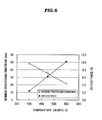
- FIG. 6 is a graph schematically showing a relationship between a temperature, and a minimum processing dimension and a reflectance when a carbon film is formed.
- the horizontal axis shows a temperature
- the vertical axis shows a minimum processing dimension in the left side and a reflectance in the right side
- FIG. 6 shows a relationship between the temperature and the minimum processing dimension, and between the temperature and the reflectance in case of forming the carbon film having a film thickness of 200 nm by the CVD method.
- the minimum processing dimension means a minimum dimension that is capable of processing without generating bend and twist of the carbon film when the RIE processing is applied to silicon oxide film as the workpiece film by using the carbon film as a mask and using a fluorocarbon (CF) based gas.
- the fifth embodiment differs from the above-mentioned embodiments in that a first region to function as a mask and a second region to function an antireflection film can be formed in the same chamber by changing the temperature condition.
- the workpiece film 2 is formed via the lower layer film 1 .
- the first region 30 to function as a mask is formed on the workpiece film 2 by the CVD method according to a first temperature condition
- the second region 40 to function as the antireflection film is formed on the first region 30 by the CVD method according to a second temperature condition changed from the first temperature condition, so as to form a first mask material film 3 A including the first and second regions 30 , 40 .
- the first mask material film 3 A is, for example, a carbon film including carbon as a main component.
- the carbon film has a tendency to be capable of providing a strength needed for a mask since the minimum processing dimension of the workpiece film 2 is reduced as the temperature at the film formation is elevated, and decreasing the reflectance of the carbon film as the temperature at the film formation is lowered. Therefore, it is preferable that the carbon film appropriate for a mask is formed at the temperature condition set to a higher temperature side in order to reduce the minimum processing dimension, and that the carbon film appropriate for the antireflection film is formed at the temperature condition set to a lower temperature side in order to reduce the reflectance. Consequently, the first temperature condition is set higher than the second temperature condition, so that the first mask material film 3 A including the first region 30 preferable as a mask and the second region 40 preferable as the antireflection film can be formed.
- a resist film is formed on the first mask material film 3 A, subsequently, a latent image of a line and space pattern is formed on the resist film by the exposure device via a reticle, and next, PEB (Post Exposure Bake) and development are carried out on the hot plate so as to form resist pattern 5 C.
- PEB Post Exposure Bake
- the resist pattern 5 C is slimmed. Further, since the resist pattern 5 C is used as a core material for forming sidewall patterns to be used as a mask, it is not particularly necessary for the resist to be formed so as to have sufficient thickness in view of the resistance properties to the dry etching.
- a second mask material film 60 is formed on the resist pattern 5 C which is slimmed, so as to have a film thickness which is almost the same as an objective pattern width.
- an etchback of the second mask material film 60 is carried out by almost the film thickness of the second mask material film 60 by using a plasma containing fluorine so that the second mask material films 60 are selectively formed as sidewall patterns on the side surfaces of the resist pattern 5 C which is the core material. Due to this, the upper surface of the resist pattern 5 C and the surface of the first mask material film 3 A being located out of a region where the resist pattern 5 C and the sidewall patterns of the second mask material film 60 are formed, are exposed.
- the resist pattern 5 c exposed and the first mask material film 3 A under the exposed resist pattern 5 c , and the first mask material film 3 A exposed are simultaneously anisotropically-etched (processed in a lump) at the same processing conditions by using, for example, a plasma containing oxygen, while leaving the second mask material film 60 .
- an etching selectivity between the first mask material film 3 A and the resist pattern 5 C which are made of an organic material, and the second mask material film 60 which is made of an inorganic material can be set to a sufficiently large value, the thickness and the aspect ratio (height:width) of the second mask material film 60 can be set to a small value similarly to the resist film to become the core pattern, and the etching can be carried out without using the wet treatment which generates stress such as surface tension, so that the line and space pattern can be formed, while being prevented from the collapse of pattern.
- the processing of the resist includes the elimination thereof.
- the pattern is transferred to the workpiece film 2 exposed under the first region 30 , by using the first mask material film 3 A to which a pattern processing is applied, particularly, the above-mentioned first region 30 as a mask based on the dry etching.
- the first mask material film 3 A to which a pattern processing is applied, particularly, the above-mentioned first region 30 as a mask based on the dry etching.
- FIG. 5H shows, as an example, a state that the second region 40 is eliminated.
- the pattern can be transferred to the workpiece film 2 by using the first mask material film 3 A as a mask after the elimination of the second mask material film 60 .
- the above-mentioned first region 30 is eliminated by a plasma ashing which uses oxygen gas, so that a line and space pattern of the workpiece film 2 can be obtained on the lower layer film 1 .
- the manufacturing processes shown in FIGS. 5F to 5I can be continuously carried out in the same chamber of a dry etching device, and can be also carried out in the different chamber respectively.
- the first region 30 to function as a mask and the second region 40 to function as an antireflection film can be separately formed by changing the first temperature condition to the second temperature condition in the same chamber in the process of forming the first mask material film 3 A by the CVD method. Therefore, for example, numbers of processes can be reduced in comparison with the case that the organic antireflection film is formed on the mask material film by separate processes, so that production costs of the semiconductor device can be reduced. Further, the collapse of pattern and the separation due to the undercut caused by poor adhesion or difference of etching rate between the antireflection film and the mask material film (carbon film) can be prevented, so that process yield can be enhanced.
- the collapse of the pattern can be effectively prevented, since in case of forming a pattern having a dimension which exceeds an exposure resolution limit in photolithography method, the pattern formation can be carried out by processing from the core material pattern to the workpiece film based on using the dry etching instead of a wet treating which causes stress between the patterns such as surface tension, while using the sidewall patterns having a low aspect ration as a mask.
- Number of processes can be reduced, since the elimination of the core material and the etching of the carbon film as a lower layer of the core material can be carried out by one process without changing the gas condition (for example, gaseous species).
- Occurrence of defect can be effectively prevented, the defect occurring, for example, due to adherence of particles at the carrying work between processes, and decrease in process yield can be reduced, since from the formation of the sidewall patterns by the etchback to the elimination of the carbon film can be carried out in one dry etching device.
- Variation in dimension can be reduced and the process yield can be enhanced, since the number of processes can be reduced.
- High-resolution resist materials can be used, since it becomes unnecessary for the resist to have the resistance properties to the dry etching.
- the sixth embodiment shows that the first mask material film having functions as a mask and an antireflection film in the fifth embodiment can be practically formed by changing the temperature condition, while providing concrete examples. Further, with regard to the same portions as the fifth embodiment, an explanation will be omitted or simplified.
- the sixth embodiment has common processes with the fifth embodiment so that it will be explained with reference to FIGS. 5A to 5I .
- the workpiece film 2 is formed via the lower layer film 1 so as to have a film thickness of 200 nm.
- the first region 30 to function as a mask is formed on the workpiece film 2 by the CVD method according to a first temperature condition so as to have a film thickness of 170 nm
- the second region 40 to function as the antireflection film is formed on the first region 30 by the CVD method according to a second temperature condition changed from the first temperature condition so as to have a film thickness of 30 nm, so that a first mask material film 3 A including the first and second regions 30 , 40 is formed so as to have a film thickness of 200 nm.
- the first and second regions 30 , 40 can be formed by continuously elevating the temperature at the film formation, and can be also formed by that after the first region 30 has been formed at the first temperature condition, the second region 40 is formed at the second temperature condition being elevated.
- the chemically-amplified ArF resist is formed so as to have a film thickness of 120 nm on the first mask material film 3 A.
- a latent image of a line and space pattern having a pitch of 80 nm and a line width of 40 nm is formed on the chemically-amplified ArF resist by the ArF liquid immersion exposure device having NA of not less than 1.3 via a reticle.
- the reflectance in the first mask material film 3 A at the time was 0.475% as a result of calculation.
- PEB Post Exposure Bake
- development are carried out on the hot plate so as to form the resist pattern 5 C having a film thickness of 100 nm.
- the line width of the resist pattern 5 C is slimmed by 20 nm.
- the slimming method includes a dry etching by a plasma containing oxygen or by a development by using TMAH (Tetra Methyl Ammonium Hydroxide) aqueous solution due to that alkaline solubilization by an acid medicinal solution is applied to the surface of the resist.
- TMAH Tetra Methyl Ammonium Hydroxide
- the slimming is carried out by developing for 30 seconds in an aqueous solution containing 2.38 wt % of TMAH and rinsing with pure water.
- the above-mentioned slimming is not indispensable, if a pattern having a desired line width can be directly formed.
- a second mask material film 60 is formed on the resist pattern 5 C which is slimmed, so as to have a film thickness of 20 nm which is almost the same as an objective pattern width.
- the second mask material film 60 includes, for example, SiO 2 , SiN, polysilicon, amorphous silicon and the like can be used.
- the film forming method includes, for example, the CVD method, the sputtering method, the coating method and the like. It is preferable that the film thickness of the second mask material film 60 is almost homogeneous, and then, LP-CVD (Lower Pressure-Chemical Vapor Deposition) method and the like can be preferably used, which can form the resist pattern 5 C at the temperature of not more than 200 degree C. at which shape degradation is not caused in the resist pattern 5 C.
- the second mask material film 60 is formed of SiO 2 by using the LP-CVD method.
- an etchback of the second mask material film 60 is carried out by almost 20 nm by using a plasma containing fluorine so that the second mask material films 60 are selectively formed as sidewall patterns on the side surfaces of the resist pattern 5 C which is the core material. Due to this, the upper surface of the resist pattern 5 C and the surface of the first mask material film 3 A being located out of a region where the resist pattern 5 C and the sidewall patterns of the second mask material film 60 are formed, are exposed.
- the resist pattern 5 c exposed and the first mask material film 3 A under the exposed resist pattern 5 c , and the first mask material film 3 A exposed are simultaneously anisotropically-etched (processed in a lump) at the same processing conditions by using, for example, a plasma containing oxygen, while leaving the second mask material film 60 .
- the aspect ratio (height:width) of the second mask material film 60 having a pitch of 40 nm and a line width of 20 nm can be set to a small value, and the processing is carried out by the dry etching instead of the wet treatment, so that the line and space pattern can be formed, while being prevented from the collapse of pattern.
- the pattern is transferred to the workpiece film 2 , by using the first mask material film 3 A, particularly, the above-mentioned first region 30 as a mask based on the dry etching.
- the above-mentioned first region 30 is eliminated by a plasma ashing which uses oxygen gas, so that a line and space pattern having a pitch of 40 nm and a line width of 20 nm of the workpiece film 2 can be obtained on the lower layer film 1 .
- FIG. 7 is a contour drawing schematically showing a relationship between a refraction index and an extinction coefficient, and the reflectance based on a simulation result in a sixth embodiment according to the invention
- FIG. 8 is a graph schematically showing a relationship between a temperature and the reflectance based on the simulation result in the sixth embodiment according to the invention.
- the horizontal axis shows a refraction index (n)
- the vertical axis shows an extinction coefficient (k)
- FIG. 7 shows that the reflectance becomes higher from the center outward.
- FIG. 7 is a contour drawing obtained by carrying out the simulation by a computer.
- the simulation is carried out for calculating the imaginary part (k) and refraction index (n) of the second region being formed as described below, by assuming a case that the first region is formed so as to have a film thickness of 170 nm at a temperature of film formation of 550 degree C., and the second region is formed on the first region so as to have a film thickness of 30 nm at a temperature of film formation which is changed, and the resist film is formed so as to have a film thickness of 120 nm.
- the reflectance has a tendency as shown in FIG. 6 , that is to say, the reflectance is decreased as the temperature at the film formation is lowered, however, according to calculation based on the film thickness and the complex refraction index, there is a lower limit in the tendency, for example, as shown in FIG. 8 . It is known that the second region 40 can be decreased in the reflectance up to almost 0.124% due to the temperature condition at the lower limit (almost 350 degree C.).
- the first region 30 to function as a mask can be formed at the first temperature condition set to a higher temperature side and the second region 40 having the reflectance which allows the second region 40 to function as an antireflection film can be formed at the second temperature condition set to a lower temperature side than the first temperature condition. Consequently, it can be said that the first mask material film 3 A having the first and second regions 30 , 40 can be adequately formed in one CVD device by changing the temperature condition.
- the resist is eliminated to form a region where a pattern does not exist, but the resist can be also left.
- the first mask material film a carbon film is used, but the other materials can be also used. Furthermore, as a method of eliminating the first mask material film, an etching can be also used.
- each of the embodiments can be arbitrarily combined, without departing from the gist of the invention.
- the process in the fourth embodiment can be carried out in the other embodiments, that the closed loop of the end portion of the line of the line and space pattern can be separated at the time of the etchback.
- each process in each of the embodiments can be changed, for example, a plurality of processed can be carried out in parallel and one process can include the other processes, without departing from the gist of the invention.
Abstract
Description
(2) Number of processes can be reduced, since the elimination of the core material and the etching of the
(3) Occurrence of defect can be effectively prevented, the defect occurring, for example, due to adherence of particles at the carrying work between processes, and decrease in process yield can be reduced, since from the elimination of the core material to the elimination of the
(4) Variation in dimension can be reduced and the process yield can be enhanced, since the number of processes can be reduced.
(5) High-resolution resist materials can be used, since it becomes unnecessary for the resist to have the resistance properties to the dry etching.
(2) The collapse of the pattern can be effectively prevented, since in case of forming a pattern having a dimension which exceeds an exposure resolution limit in photolithography method, the pattern formation can be carried out by processing from the core material pattern to the workpiece film based on using the dry etching instead of a wet treating which causes stress between the patterns such as surface tension, while using the sidewall patterns having a low aspect ration as a mask.
(3) Number of processes can be reduced, since the elimination of the core material and the etching of the carbon film as a lower layer of the core material can be carried out by one process without changing the gas condition (for example, gaseous species).
(4) Occurrence of defect can be effectively prevented, the defect occurring, for example, due to adherence of particles at the carrying work between processes, and decrease in process yield can be reduced, since from the formation of the sidewall patterns by the etchback to the elimination of the carbon film can be carried out in one dry etching device.
(5) Variation in dimension can be reduced and the process yield can be enhanced, since the number of processes can be reduced.
(6) High-resolution resist materials can be used, since it becomes unnecessary for the resist to have the resistance properties to the dry etching.
Claims (17)
Applications Claiming Priority (4)
| Application Number | Priority Date | Filing Date | Title |
|---|---|---|---|
| JP2008-152016 | 2008-06-10 | ||
| JP2008152016A JP5224919B2 (en) | 2008-06-10 | 2008-06-10 | Manufacturing method of semiconductor device |
| JP2009046313A JP5275085B2 (en) | 2009-02-27 | 2009-02-27 | Manufacturing method of semiconductor device |
| JP2009-046313 | 2009-02-27 |
Publications (2)
| Publication Number | Publication Date |
|---|---|
| US20090305166A1 US20090305166A1 (en) | 2009-12-10 |
| US8329385B2 true US8329385B2 (en) | 2012-12-11 |
Family
ID=41400623
Family Applications (1)
| Application Number | Title | Priority Date | Filing Date |
|---|---|---|---|
| US12/481,919 Active 2030-11-09 US8329385B2 (en) | 2008-06-10 | 2009-06-10 | Method of manufacturing a semiconductor device |
Country Status (1)
| Country | Link |
|---|---|
| US (1) | US8329385B2 (en) |
Cited By (1)
| Publication number | Priority date | Publication date | Assignee | Title |
|---|---|---|---|---|
| US8994088B2 (en) | 2012-09-10 | 2015-03-31 | Kabushiki Kaisha Toshiba | Semiconductor storage device and manufacturing method thereof |
Families Citing this family (4)
| Publication number | Priority date | Publication date | Assignee | Title |
|---|---|---|---|---|
| US7790360B2 (en) * | 2007-03-05 | 2010-09-07 | Micron Technology, Inc. | Methods of forming multiple lines |
| JP5361406B2 (en) | 2009-01-20 | 2013-12-04 | 株式会社東芝 | Manufacturing method of semiconductor device |
| JP2011129756A (en) * | 2009-12-18 | 2011-06-30 | Toshiba Corp | Method of generating mask pattern, mask pattern generating program, and method of manufacturing semiconductor device |
| CN103839781B (en) * | 2012-11-21 | 2016-05-25 | 中芯国际集成电路制造(上海)有限公司 | The formation method of semiconductor fine pattern |
Citations (13)
| Publication number | Priority date | Publication date | Assignee | Title |
|---|---|---|---|---|
| US4803181A (en) | 1986-03-27 | 1989-02-07 | International Business Machines Corporation | Process for forming sub-micrometer patterns using silylation of resist side walls |
| JPH03270227A (en) | 1990-03-20 | 1991-12-02 | Mitsubishi Electric Corp | Formation of fine pattern |
| US6063688A (en) | 1997-09-29 | 2000-05-16 | Intel Corporation | Fabrication of deep submicron structures and quantum wire transistors using hard-mask transistor width definition |
| JP2000310850A (en) | 1999-02-22 | 2000-11-07 | Toshiba Corp | Exposure monitor mask, exposure regulation method and production of semiconductor device |
| JP2001102282A (en) | 1999-09-28 | 2001-04-13 | Toshiba Corp | Methdo for controlling aligner and method for controlling semiconductor manufacturing apparatus |
| US20020001778A1 (en) * | 2000-06-08 | 2002-01-03 | Applied Materials, Inc. | Photolithography scheme using a silicon containing resist |
| JP2002025895A (en) | 2000-07-07 | 2002-01-25 | Toshiba Corp | Exposure measurement method and exposure measurement device |
| US20020037637A1 (en) * | 2000-08-10 | 2002-03-28 | Guoqiang Xing | Using a carbon film as an etch hardmask for hard-to-etch materials |
| JP3270227B2 (en) | 1993-05-26 | 2002-04-02 | 富士写真フイルム株式会社 | Electric hoist |
| JP2002299205A (en) | 2001-03-29 | 2002-10-11 | Toshiba Corp | Method for controlling semiconductor manufacturing device |
| US20040102048A1 (en) | 2002-11-25 | 2004-05-27 | Renesas Technology Corp. | Method for manufacturing semiconductor device |
| US20060240359A1 (en) * | 2005-04-22 | 2006-10-26 | Chih-Hung Liu | Patterning process and contact structure |
| US20080122125A1 (en) * | 2006-11-29 | 2008-05-29 | Micron Technology, Inc. | Methods to reduce the critical dimension of semiconductor devices and partially fabricated semiconductor devices having reduced critical dimensions |
-
2009
- 2009-06-10 US US12/481,919 patent/US8329385B2/en active Active
Patent Citations (16)
| Publication number | Priority date | Publication date | Assignee | Title |
|---|---|---|---|---|
| US4803181A (en) | 1986-03-27 | 1989-02-07 | International Business Machines Corporation | Process for forming sub-micrometer patterns using silylation of resist side walls |
| JPH03270227A (en) | 1990-03-20 | 1991-12-02 | Mitsubishi Electric Corp | Formation of fine pattern |
| JP3270227B2 (en) | 1993-05-26 | 2002-04-02 | 富士写真フイルム株式会社 | Electric hoist |
| US6063688A (en) | 1997-09-29 | 2000-05-16 | Intel Corporation | Fabrication of deep submicron structures and quantum wire transistors using hard-mask transistor width definition |
| JP2000310850A (en) | 1999-02-22 | 2000-11-07 | Toshiba Corp | Exposure monitor mask, exposure regulation method and production of semiconductor device |
| US6226074B1 (en) | 1999-02-22 | 2001-05-01 | Kabushiki Kaisha Toshiba | Exposure monitor mask, exposure adjusting method and method of manufacturing semiconductor devices |
| US6376139B1 (en) | 1999-09-28 | 2002-04-23 | Kabushiki Kaisha Toshiba | Control method for exposure apparatus and control method for semiconductor manufacturing apparatus |
| JP2001102282A (en) | 1999-09-28 | 2001-04-13 | Toshiba Corp | Methdo for controlling aligner and method for controlling semiconductor manufacturing apparatus |
| US20020001778A1 (en) * | 2000-06-08 | 2002-01-03 | Applied Materials, Inc. | Photolithography scheme using a silicon containing resist |
| JP2002025895A (en) | 2000-07-07 | 2002-01-25 | Toshiba Corp | Exposure measurement method and exposure measurement device |
| US20020037637A1 (en) * | 2000-08-10 | 2002-03-28 | Guoqiang Xing | Using a carbon film as an etch hardmask for hard-to-etch materials |
| JP2002299205A (en) | 2001-03-29 | 2002-10-11 | Toshiba Corp | Method for controlling semiconductor manufacturing device |
| US20020182521A1 (en) | 2001-03-29 | 2002-12-05 | Kabushiki Kaisha Toshiba | Method of manufacturing semiconductor device |
| US20040102048A1 (en) | 2002-11-25 | 2004-05-27 | Renesas Technology Corp. | Method for manufacturing semiconductor device |
| US20060240359A1 (en) * | 2005-04-22 | 2006-10-26 | Chih-Hung Liu | Patterning process and contact structure |
| US20080122125A1 (en) * | 2006-11-29 | 2008-05-29 | Micron Technology, Inc. | Methods to reduce the critical dimension of semiconductor devices and partially fabricated semiconductor devices having reduced critical dimensions |
Cited By (1)
| Publication number | Priority date | Publication date | Assignee | Title |
|---|---|---|---|---|
| US8994088B2 (en) | 2012-09-10 | 2015-03-31 | Kabushiki Kaisha Toshiba | Semiconductor storage device and manufacturing method thereof |
Also Published As
| Publication number | Publication date |
|---|---|
| US20090305166A1 (en) | 2009-12-10 |
Similar Documents
| Publication | Publication Date | Title |
|---|---|---|
| US7576010B2 (en) | Method of forming pattern using fine pitch hard mask | |
| US6803661B2 (en) | Polysilicon processing using an anti-reflective dual layer hardmask for 193 nm lithography | |
| KR101203201B1 (en) | Semiconductor device manufacturing method | |
| US7575992B2 (en) | Method of forming micro patterns in semiconductor devices | |
| US8728945B2 (en) | Method for patterning sublithographic features | |
| US9128384B2 (en) | Method of forming a pattern | |
| US7550384B2 (en) | Semiconductor device and method for forming pattern in the same | |
| KR100723506B1 (en) | Method of forming micro-patterns using multiple photolithography process | |
| US8329385B2 (en) | Method of manufacturing a semiconductor device | |
| JP2009158907A (en) | Fine pattern forming method of semiconductor element | |
| US11769691B2 (en) | Semiconductor device and formation method thereof | |
| US20230350283A1 (en) | Euv photo masks and manufacturing method thereof | |
| US20090246954A1 (en) | Method of manufacturing semiconductor device | |
| KR20220044075A (en) | Semiconductor patterning and resulting structures | |
| JP2009302143A (en) | Manufacturing method of semiconductor device | |
| US20090130850A1 (en) | Semiconductor Devices and Method of Fabricating the Same | |
| CN114334619A (en) | Method for forming semiconductor structure | |
| US8084832B2 (en) | Semiconductor device | |
| TWI443758B (en) | Method of forming gate conductor structures | |
| US7939451B2 (en) | Method for fabricating a pattern | |
| CN111640657B (en) | Semiconductor device and method of forming the same | |
| KR100489360B1 (en) | A fabricating method of semiconductor device using ArF photolithography | |
| US7199034B1 (en) | Flash memory device and method for fabricating the same | |
| US7674708B2 (en) | Method for forming fine patterns of a semiconductor device | |
| KR20110060757A (en) | Method for manufacturing semiconductor device |
Legal Events
| Date | Code | Title | Description |
|---|---|---|---|
| AS | Assignment |
Owner name: KABUSHIKI KAISHA TOSHIBA, JAPAN Free format text: ASSIGNMENT OF ASSIGNORS INTEREST;ASSIGNORS:SHIOBARA, EISHI;KIKUTANI, KEISUKE;YAHIRO, KAZUYUKI;AND OTHERS;REEL/FRAME:022806/0839 Effective date: 20090605 |
|
| STCF | Information on status: patent grant |
Free format text: PATENTED CASE |
|
| FEPP | Fee payment procedure |
Free format text: PAYOR NUMBER ASSIGNED (ORIGINAL EVENT CODE: ASPN); ENTITY STATUS OF PATENT OWNER: LARGE ENTITY |
|
| FPAY | Fee payment |
Year of fee payment: 4 |
|
| AS | Assignment |
Owner name: TOSHIBA MEMORY CORPORATION, JAPAN Free format text: ASSIGNMENT OF ASSIGNORS INTEREST;ASSIGNOR:KABUSHIKI KAISHA TOSHIBA;REEL/FRAME:043709/0035 Effective date: 20170706 |
|
| MAFP | Maintenance fee payment |
Free format text: PAYMENT OF MAINTENANCE FEE, 8TH YEAR, LARGE ENTITY (ORIGINAL EVENT CODE: M1552); ENTITY STATUS OF PATENT OWNER: LARGE ENTITY Year of fee payment: 8 |
|
| AS | Assignment |
Owner name: K.K. PANGEA, JAPAN Free format text: MERGER;ASSIGNOR:TOSHIBA MEMORY CORPORATION;REEL/FRAME:055659/0471 Effective date: 20180801 Owner name: TOSHIBA MEMORY CORPORATION, JAPAN Free format text: CHANGE OF NAME AND ADDRESS;ASSIGNOR:K.K. PANGEA;REEL/FRAME:055669/0401 Effective date: 20180801 Owner name: KIOXIA CORPORATION, JAPAN Free format text: CHANGE OF NAME AND ADDRESS;ASSIGNOR:TOSHIBA MEMORY CORPORATION;REEL/FRAME:055669/0001 Effective date: 20191001 |