US8330761B2 - Apparatus and method for reducing output rate of video data - Google Patents
Apparatus and method for reducing output rate of video data Download PDFInfo
- Publication number
- US8330761B2 US8330761B2 US12/010,374 US1037408A US8330761B2 US 8330761 B2 US8330761 B2 US 8330761B2 US 1037408 A US1037408 A US 1037408A US 8330761 B2 US8330761 B2 US 8330761B2
- Authority
- US
- United States
- Prior art keywords
- frame
- rate
- width
- video
- adjusted
- Prior art date
- Legal status (The legal status is an assumption and is not a legal conclusion. Google has not performed a legal analysis and makes no representation as to the accuracy of the status listed.)
- Active, expires
Links
- 238000000034 method Methods 0.000 title claims abstract description 30
- 238000012545 processing Methods 0.000 claims abstract description 13
- 238000011084 recovery Methods 0.000 claims description 6
- 238000010586 diagram Methods 0.000 description 8
- 230000005540 biological transmission Effects 0.000 description 6
- 230000008878 coupling Effects 0.000 description 2
- 238000010168 coupling process Methods 0.000 description 2
- 238000005859 coupling reaction Methods 0.000 description 2
- 238000012986 modification Methods 0.000 description 2
- 230000004048 modification Effects 0.000 description 2
- 230000002035 prolonged effect Effects 0.000 description 2
- 230000000630 rising effect Effects 0.000 description 2
- 238000012546 transfer Methods 0.000 description 2
- 101000805129 Homo sapiens Protein DPCD Proteins 0.000 description 1
- 102100037836 Protein DPCD Human genes 0.000 description 1
- 238000009825 accumulation Methods 0.000 description 1
- 230000002457 bidirectional effect Effects 0.000 description 1
- 230000015572 biosynthetic process Effects 0.000 description 1
- 238000006243 chemical reaction Methods 0.000 description 1
- 238000010276 construction Methods 0.000 description 1
- 239000013078 crystal Substances 0.000 description 1
- 238000013507 mapping Methods 0.000 description 1
- 238000005070 sampling Methods 0.000 description 1
- 238000003786 synthesis reaction Methods 0.000 description 1
- XLYOFNOQVPJJNP-UHFFFAOYSA-N water Substances O XLYOFNOQVPJJNP-UHFFFAOYSA-N 0.000 description 1
Images


Classifications
-
- G—PHYSICS
- G09—EDUCATION; CRYPTOGRAPHY; DISPLAY; ADVERTISING; SEALS
- G09G—ARRANGEMENTS OR CIRCUITS FOR CONTROL OF INDICATING DEVICES USING STATIC MEANS TO PRESENT VARIABLE INFORMATION
- G09G5/00—Control arrangements or circuits for visual indicators common to cathode-ray tube indicators and other visual indicators
- G09G5/003—Details of a display terminal, the details relating to the control arrangement of the display terminal and to the interfaces thereto
- G09G5/006—Details of the interface to the display terminal
Definitions
- the invention relates to video interface and more particularly, to an apparatus and method for reducing output rate of video data for DisplayPort receiver.
- FIG. 1 shows a schematic diagram illustrating a DisplayPort interface 130 coupling a source device 110 with a sink device 120 , and the data flow through the interface.
- DisplayPort is a new digital display interface standard put forth by the Video Electronics Standard Association (VESA). As shown in FIG. 1 , the DisplayPort interface 130 consists of a Main Link, an auxiliary channel (AUX CH), and a hot plug detect (HPD) signal line.
- the auxiliary channel with low-latency (each transaction taking no longer than 500 ⁇ s), providing for 1 Mbps of data rate of auxiliary nature, is a half-duplex bidirectional channel used for main link management and device control (upon the source device 110 and the sink device 120 ).
- the HPD signal line can serve to issue an interrupt request by the sink device (or receiver) 120 to the source device (or transmitter) 110 .
- Main Link is a high-bandwidth, low-delay, uni-directional interface for isochronous streaming.
- the number of lanes of Main Link can be either 1, 2, or 4 lanes, for providing for simultaneous digital video and audio streaming transmission.
- Each lane supports transmission at two link rates (F link ): 1.62 Gbps or 2.7 Gbps per lane. Therefore, DisplayPort offers up to 10.8 Gbps of bandwidth.
- F link link rate
- F sym indicates the data-transfer rate in terms of symbol over the Main Link.
- the link symbol rate F link is defined as 1/10 of the link rate F link through downsampling; therefore two link symbol rate F sym can be observed: 162 Mbps and 270 Mbps.
- the pixel rate F pix decoupled from the link symbol rate F sym and the link rate F link , refers to the pixel (each pixel generally containing 24 bits, i.e., all RGB data) transfer rate of the source device 110 .
- DisplayPort requires no dedicated channel for forwarding clock.
- the sink device 120 utilizes data recovery strategy to recover the link symbol rate F sym from the received data streams. While utilizing the DisplayPort to transmit data, the source device 110 generates the pixel data at a pixel rate F pix , which is decoupled from the link rate F link .
- the source device 110 delivers time stamp values M vid [23:0], N vid [23:0] to the sink device 120 by means of frequency ratio packets (the frequency ratio packets also contain the audio time stamp values M aud and N aud , which are not to be discussed herein) or stream attribute packets specified by DisplayPort standard, according to which the sink device 120 is able to recover a pixel clock CLK pix having the pixel rate F pix .
- the sink device 120 can recover the pixel clock CLK pix or the pixel rate F pix of the transmit device 110 according to the link symbol clock CLK sym (having the link symbol rate F sym ) the time stamp values M vid , N vid , and a circuit configuration, as shown in FIG.
- FIG. 3A shows a diagram illustrating relevant image attribute parameters of a frame.
- FIG. 3B shows a timing diagram illustrating the relationship of a vertical synchronization signal VS, a horizontal synchronization signal HS, and a data enable signal DE.
- the main stream attribute packet transmitted by the source device 110 further contains the following image attribute parameters (referring to FIG.
- a frame width H total a frame height V total , a left blanking width H start , a top blanking height V start , an active area width H width , an active area height V height , a vertical synchronization width W VS , a horizontal synchronization width W HS , and so forth, which are provided for the sink device 120 to recover the original frame format, i.e., both the size and relative location of the active area 310 and the blanking (or non-active) area 320 in a frame.
- the sink device 120 utilizes the above-mentioned recovered pixel rate F pix as the sampling frequency for transmitting the video data to the back-end circuit, and subsequently constructs or recovers image control signals according to the above-mentioned image attribute parameters.
- a vertical synchronization signal VS is constructed according to a pixel period T pix and the vertical synchronizing width W VS (in terms of pixel periods)
- the horizontal synchronizing signal HS is constructed according to the pixel period T pix , the frame width H total , and the horizontal synchronization width W HS (in terms of the pixel periods).
- the data enable signal DE and a field signal FIELD are constructed according to the pixel period T pix , the left blanking width H start , and the active area width H width , so that the video data can be further processed according thereto.
- the sink device 120 is designed only to recover the original pixel clock CLK pix .
- the sink device 120 will be a need for the sink device 120 to reduce the pixel rate F pix when the back-end circuit includes either components requiring a large amount of computation such as a scaler, or a display monitor having a lower display frequency, or is limited to the physical constraint of printed circuit boards.
- the output rate of video data (or pixel rate) needs to be reduced to become compatible with more types of back-end circuits.
- an object of the invention is to provide a method for reducing output rate of video data, which achieves the goal of reducing a pixel rate by fully or partially utilizing a blanking area in a frame format.
- the method for reducing output rate of video data for a sink device having a digital display interface comprises the steps of: storing input video data in a buffer according to a link symbol clock; calculating a period of a first frame according to a width of the first frame and a height of the first frame, a ratio of time stamp values and a link symbol clock having the link symbol rate; determining a second pixel rate of the sink device according to a format of the first frame and the period of the first frame; and, generating at least a control signal to access the input video data that stores in the buffer according to a second pixel clock having the second pixel rate.
- Another object of the invention is to provide a video receiver, comprising: a clock data recovery circuit for receiving a video data and generating a video data and a clock signal; a decoder coupled to the clock data recovery circuit for decoding the video data and generating a decoded video data and a set of original image attribute parameters; a video buffer coupled to the decoder for temporarily storing the decoded video data; a processing circuit coupled to the decoder for generating a set of adjusted image attribute parameters and a set of setting values according to the set of the original image attribute parameters; a clock generator coupled to the processing circuit for generating an adjusted pixel clock; and, a control signal generator for generating a set of adjusted video control signals according to the set of the adjusted image attribute parameters and the adjusted pixel clock.
- a frame period T frame is fixed first. Then, according to the processing rate limit of the back-end circuit, the size of the blanking area in an original frame format and the storage capacity of the video buffer, a pixel rate most suitable for the processing rate of the sink device is determined and thus corresponding control signals Req, HS′, VS′, DE′, FIELD′ are generated.
- FIG. 1 shows a schematic diagram illustrating a DisplayPort interface coupling a source device with a sink device, and the data flow through the interface.
- FIG. 2 shows a phase-locked loop coupled with two frequency dividers for recovering a pixel rate from a link symbol rate in a DisplayPort sink device.
- FIG. 3A shows a diagram illustrating relevant image attribute parameters of a frame.
- FIG. 3B shows a timing diagram illustrating the relationship of a vertical synchronization signal VS, a horizontal synchronization signal HS, and a data enable signal DE.
- FIG. 4 is a timing diagram showing the relationship among a vertical blanking signal VB, vertical synchronization signals VS, VS′, and data enable signals DE, DE′ according to the invention.
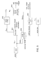
- FIG. 5 shows a data flow in a portion of a DisplayPort sink device according to the invention.
- FIG. 6 is a data flow showing a method for reducing output rate of video data according to the invention.
- DisplayPort requires no dedicated channel for forwarding clock, so the sink device 120 is supposed to recover the original pixel clock CLK pix . On the other hand, this affords to the sink device 120 a great opportunity to establish a pixel rate that fits the processing rate of its own or the back-end circuit.
- the invention offers the flexibility in reducing the pixel rate F pix by means of reducing the blank area in the original frame format.
- FIG. 4 is a timing diagram showing the relationship among a vertical blanking signal VB, vertical synchronization signals VS, VS′, and data enable signals DE, DE′ according to the invention.
- the vertical synchronization signals VS and the data enable signals DE are the original signals generated by the source device 110
- the vertical synchronization signals VS′ and data enable signals DE′ are recovered signals by the sink device 120 after reducing the pixel rate (or prolonging the pixel period).
- the sink device 120 In order not to affect the data volume and the contents of the active area, the sink device 120 has to maintain the same vertical refresh rate as the source device 110 does, thus maintaining a stable water-level in the FIFO (such as the video FIFO 530 of FIG. 5 ) where video data are stored. In other words, as long as the vertical synchronization signals VS′ that the sink device 120 reconstructs continues to align with the vertical blanking signal VB (as shown in FIG. 4 ), the sink device 120 will be able to maintain the same vertical refresh rate as the source device 110 does.
- the vertical synchronization signals VS′ has to maintain a specific relationship with the vertical blanking signal VB; for example, all rising edges of the vertical synchronization signals VS′ have to lag behind all rising edges of the vertical blanking signal VB by a predefined period T d , to avoid skipping or no data available.
- the sink device 120 measures the length of a frame period T frame using a fixed reference clock, such as a crystal clock.
- a fixed reference clock such as a crystal clock.
- the number of pixels that a frame includes is equal to the product of the frame width H total and the frame height V total ; therefore, each original pixel period T pix in the source device 110 is equal to the frame period T frame divided by the product of the frame width H total and the frame height V total .
- the frame width H total is equal to the active area width H width plus the blanking (or non-active) area width H porch
- the frame height V total is equal to the active area height V width plus the blanking (or non-active) area height V porch .
- the sink device 120 can achieve the goal of reducing the output rate of video data (or the pixel rate) by reducing either the blanking area width H porch or the blanking area height V porch .
- an enable (logic-high) period of a data enable signal DE′ in the sink device 120 can be prolonged if a disable (logic-low) period of the data enable signal DE′ (i.e., the non-active area) is reduced; on condition that the data volume of the active area is fixed, a pixel period T′ pix then has the flexibility to be prolonged and the pixel rate F′ pix be reduced.
- the degree of decrease in pixel rate F′ pix apparently corresponds both to the degree of decrease in the blanking area width H′ porch and the degree of decrease in the blanking area height V′ porch .
- the degree of decrease in pixel rate F′ pix corresponds to the size of the blanking area in the original frame format. Consequently, the degree of decrease in pixel rate F′ pix will be limited if the original blanking area, or non-active area or porch period, in the data enable signal DE is narrow.
- FIG. 5 shows a data flow in a portion of a DisplayPort sink device according to the invention.
- a clock data recovery circuit 510 coupled to one of the four lanes of the main link, recovers a link symbol clock CLK′ sym (possibly slightly different from the link symbol clock CLK sym that the source device 110 actually generates) based on the received video data and correctly receives video data D sym .
- the decoded video data D vid is stored in the video FIFO 530 according to the link symbol clock CLK′ sym . Subsequently, to ensure that the back-end circuit functions normally, the data D vid is transmitted according to a slower pixel clock CLK′ pix having a pixel rate F′ pix while outputted from the video FIFO 530 .
- the video FIFO 530 is used to serve as buffer for accumulation of data amount caused by a difference in transmission rate between the two pixel clocks. Obviously, the larger the size of the video FIFO 530 is, the more the difference between the rates of the two pixel clocks are allowed, indicating an increased flexibility in reducing the pixel rate.
- the decision unit 560 acknowledges the size of the blanking area in the original frame format according to original image attribute parameters, and also determines new image attribute parameters H′ total , V′ total , H′ start , V′ start and a new pixel period T′ pix (or a new pixel rate F′ pix ) according to the current pixel rate, the time stamp values M vid , N vid , the processing rate limit of the back-end circuit, and the storage capacity of the video FIFO 530 .
- the decision unit 560 In order for a clock generator 550 (which can be implemented as a phased lock loop, or PLL) to generate the pixel clock CLK′ pix , having the pixel rate F′ pix , the decision unit 560 first generates corresponding setting values to set the clock generator 550 . Next, the clock generator 550 generates the pixel clock CLK′ pix having the pixel rate F′ pix based upon the link symbol rate CLK′ sym (or an independent clock source) and said setting values.
- a clock generator 550 which can be implemented as a phased lock loop, or PLL
- a control signal generator 540 receives the parameters W VS , W HS , H width , V height and new image attribute parameters H′ total , V′ total , H′ start , V′ start that the decision unit 560 provides, to generate new control signals Req, HS, VS, DE, FIELD.
- FIG. 6 is a data flow showing a method for reducing output rate of video data according to the invention.
- the method for reducing output rate of video data of the invention will be hereinafter detailed with reference to FIGS. 5 and 6 .
- Step S 610 a frame period T frame is calculated.
- the decision unit 560 first accesses the DPCD circuit 570 to obtain a current link rate F link (1.62 Gbps or 2.7 Gbps) and then reduces the current link rate F link to 10% so as to obtain the link symbol rate F sym (162 Mbps or 270 Mbps).
- Step S 620 according to the image attribute parameters H total , V total , H start , V start , H width , and V height , the size of the blanking area (or non-active area) in an original frame is determined.
- Step S 630 according to the processing rate of the back-end circuit, the storage capacity of the video FIFO 530 , and the size of the blanking area, new image attribute parameters H′ total , V′ total , H′ start , and V′ start are determined.
- the decision unit 560 has to generate corresponding setting values in advance to set the clock generator 550 . For example, by means of setting a current value of a charge pump or adjusting dividers (not shown), the decision unit 560 causes the clock generator 550 to generate the clock CLK′ pix according to either the link symbol rate CLK′ sym or an independent clock source.
- the clock CLK′ pix having the period T′ pix can be generated by using direct digital synthesis, or by referring to the link symbol rate CLK′ sym or the independent clock source.
- Step S 650 according to the clock CLK′ pix and the image attribute parameters W VS , W HS , H′ total , V′ total , H′ start , and V′ start , the control signal generator 540 generates the control signals HS′, VS′, DE′ (similar to those in FIG. 3B , but having longer pixel periods and smaller blanking sizes as shown in FIG. 4 ), and FIELD′. It should be noted that before generating the control signal DE′, the control signal generator 540 will issue a request signal Req to notify the video FIFO 530 to get video data ready. After a pre-defined time has elapsed, the control signal generator 540 and the video FIFO 530 synchronously transmit the control signal DE′ and the video data D vid to the back-end circuit.
- the frame period T frame has to be fixed first in order to achieve the goal of reducing the pixel rate. Then, a degree of decrease of the pixel rate is determined according to the processing rate limit of the back-end circuit. Next, the size of the blanking area in the original frame format is examined. The degree of decrease of the pixel rate is limited if the size of the blanking area is small or the storage capacity of the video FIFO 530 is not large enough. On the contrary, if the size of the blanking area and the storage capacity of the video buffer 530 are large enough, the goal of reducing the pixel rate can be easily achieved.
Abstract
Description
Claims (24)
Applications Claiming Priority (3)
| Application Number | Priority Date | Filing Date | Title |
|---|---|---|---|
| TW096102935 | 2007-01-26 | ||
| TW96102935A | 2007-01-26 | ||
| TW096102935A TWI360803B (en) | 2007-01-26 | 2007-01-26 | Apparatus and method for reducing output speed of |
Publications (2)
| Publication Number | Publication Date |
|---|---|
| US20080211821A1 US20080211821A1 (en) | 2008-09-04 |
| US8330761B2 true US8330761B2 (en) | 2012-12-11 |
Family
ID=39732759
Family Applications (1)
| Application Number | Title | Priority Date | Filing Date |
|---|---|---|---|
| US12/010,374 Active 2031-10-13 US8330761B2 (en) | 2007-01-26 | 2008-01-24 | Apparatus and method for reducing output rate of video data |
Country Status (2)
| Country | Link |
|---|---|
| US (1) | US8330761B2 (en) |
| TW (1) | TWI360803B (en) |
Cited By (3)
| Publication number | Priority date | Publication date | Assignee | Title |
|---|---|---|---|---|
| US20120068993A1 (en) * | 2010-09-20 | 2012-03-22 | Srikanth Kambhatla | Techniques for changing image display properties |
| US20130278591A1 (en) * | 2012-04-24 | 2013-10-24 | Silicon Works Co., Ltd. | Embedded displayport system and method for controlling panel self refresh mode |
| US20140168234A1 (en) * | 2012-12-18 | 2014-06-19 | Apple Inc. | Low power display port with arbitrary link clock frequency |
Families Citing this family (4)
| Publication number | Priority date | Publication date | Assignee | Title |
|---|---|---|---|---|
| US20120182473A1 (en) * | 2011-01-14 | 2012-07-19 | Gyudong Kim | Mechanism for clock recovery for streaming content being communicated over a packetized communication network |
| TWI651002B (en) * | 2017-08-30 | 2019-02-11 | 北京集創北方科技股份有限公司 | Signal transmission device |
| TWI701647B (en) * | 2019-07-10 | 2020-08-11 | 大陸商北京歐錸德微電子技術有限公司 | Picture display method, display device and information processing device capable of automatically adjusting frame rate |
| CN111510772B (en) * | 2020-03-23 | 2022-03-29 | 珠海亿智电子科技有限公司 | Method, device, equipment and storage medium for balancing video frame rate error |
Citations (9)
| Publication number | Priority date | Publication date | Assignee | Title |
|---|---|---|---|---|
| US5765197A (en) * | 1993-12-16 | 1998-06-09 | International Business Machines Corporation | Method and system for authentication of a memory unit for a computer system |
| US20060050075A1 (en) * | 2004-09-08 | 2006-03-09 | Gong Jin S | Method for frame rate conversion |
| US20060071922A1 (en) | 2004-10-05 | 2006-04-06 | Yu-Pin Chou | Device and method for up/down converting data output |
| US20070002169A1 (en) * | 2005-06-29 | 2007-01-04 | Microsoft Corporation | Detecting progressive video |
| US7487273B2 (en) * | 2003-09-18 | 2009-02-03 | Genesis Microchip Inc. | Data packet based stream transport scheduler wherein transport data link does not include a clock line |
| US7599439B2 (en) * | 2005-06-24 | 2009-10-06 | Silicon Image, Inc. | Method and system for transmitting N-bit video data over a serial link |
| US7911536B2 (en) * | 2004-09-23 | 2011-03-22 | Intel Corporation | Screen filled display of digital video content |
| US7995143B2 (en) * | 2006-02-10 | 2011-08-09 | Qualcomm Incorporated | Wireless video link synchronization |
| US8051217B2 (en) * | 2007-01-12 | 2011-11-01 | Dell Products L.P. | System and method for providing PCIe over displayport |
-
2007
- 2007-01-26 TW TW096102935A patent/TWI360803B/en active
-
2008
- 2008-01-24 US US12/010,374 patent/US8330761B2/en active Active
Patent Citations (9)
| Publication number | Priority date | Publication date | Assignee | Title |
|---|---|---|---|---|
| US5765197A (en) * | 1993-12-16 | 1998-06-09 | International Business Machines Corporation | Method and system for authentication of a memory unit for a computer system |
| US7487273B2 (en) * | 2003-09-18 | 2009-02-03 | Genesis Microchip Inc. | Data packet based stream transport scheduler wherein transport data link does not include a clock line |
| US20060050075A1 (en) * | 2004-09-08 | 2006-03-09 | Gong Jin S | Method for frame rate conversion |
| US7911536B2 (en) * | 2004-09-23 | 2011-03-22 | Intel Corporation | Screen filled display of digital video content |
| US20060071922A1 (en) | 2004-10-05 | 2006-04-06 | Yu-Pin Chou | Device and method for up/down converting data output |
| US7599439B2 (en) * | 2005-06-24 | 2009-10-06 | Silicon Image, Inc. | Method and system for transmitting N-bit video data over a serial link |
| US20070002169A1 (en) * | 2005-06-29 | 2007-01-04 | Microsoft Corporation | Detecting progressive video |
| US7995143B2 (en) * | 2006-02-10 | 2011-08-09 | Qualcomm Incorporated | Wireless video link synchronization |
| US8051217B2 (en) * | 2007-01-12 | 2011-11-01 | Dell Products L.P. | System and method for providing PCIe over displayport |
Non-Patent Citations (1)
| Title |
|---|
| DisplayPort Technical Overview, Oct. 27, 2005. |
Cited By (6)
| Publication number | Priority date | Publication date | Assignee | Title |
|---|---|---|---|---|
| US20120068993A1 (en) * | 2010-09-20 | 2012-03-22 | Srikanth Kambhatla | Techniques for changing image display properties |
| US8842111B2 (en) * | 2010-09-20 | 2014-09-23 | Intel Corporation | Techniques for selectively changing display refresh rate |
| US20130278591A1 (en) * | 2012-04-24 | 2013-10-24 | Silicon Works Co., Ltd. | Embedded displayport system and method for controlling panel self refresh mode |
| US9286841B2 (en) * | 2012-04-24 | 2016-03-15 | Silicon Works Co., Ltd. | Embedded DisplayPort system and method for controlling panel self refresh mode |
| US20140168234A1 (en) * | 2012-12-18 | 2014-06-19 | Apple Inc. | Low power display port with arbitrary link clock frequency |
| US9013493B2 (en) * | 2012-12-18 | 2015-04-21 | Apple Inc. | Low power display port with arbitrary link clock frequency |
Also Published As
| Publication number | Publication date |
|---|---|
| US20080211821A1 (en) | 2008-09-04 |
| TW200832349A (en) | 2008-08-01 |
| TWI360803B (en) | 2012-03-21 |
Similar Documents
| Publication | Publication Date | Title |
|---|---|---|
| US8330761B2 (en) | Apparatus and method for reducing output rate of video data | |
| US8156238B2 (en) | Wireless multimedia transport method and apparatus | |
| TWI488172B (en) | Multi-monitor display | |
| US8724024B2 (en) | Video signal output device and method | |
| US8503490B2 (en) | Information processing apparatus, information processing method, and program | |
| JP6008141B2 (en) | Baseband video data transmission device, reception device, and transmission / reception system | |
| US8331460B2 (en) | Video sink device | |
| US20120257680A1 (en) | Digital video transmission | |
| CN101354878B (en) | Receiving apparatus and clock signal rate calibration method | |
| US9160959B2 (en) | Transmission device, transmission method, reception device, reception method, and transmission/reception system | |
| WO2018128879A1 (en) | Branch device bandwidth management for video streams | |
| CN101431643B (en) | Apparatus and method for reducing video data output speed | |
| US20110170003A1 (en) | Information processing apparatus, information processing method, and program | |
| US20080129871A1 (en) | Video and Audio Synchronization Method and Related Apparatus for a Multimedia Interface | |
| US7250980B2 (en) | Automatic detection of sync polarity in video timing and generation of blanking period indicator from sync information | |
| CN101202868B (en) | Image and sound data synchronization method for multimedia interface and related device | |
| TWI774434B (en) | Transmission control system of multi-media signal, transmission control circuit and receiving control circuit | |
| CN117440122A (en) | HDMI device and power saving method | |
| Wiley | 40.1: Invited paper: Displayport® 1.2, embedded displayport, and future trends | |
| JP2003143499A (en) | Digital television receiver, video data transmission circuit and video data reception circuit | |
| JP2017122867A (en) | Timing controller |
Legal Events
| Date | Code | Title | Description |
|---|---|---|---|
| AS | Assignment |
Owner name: REALTEK SEMICONDUCTOR CORP., TAIWAN Free format text: ASSIGNMENT OF ASSIGNORS INTEREST;ASSIGNORS:LIN, TZUO-BO;KUNG, WEN-HSIA;REEL/FRAME:020466/0613;SIGNING DATES FROM 20071108 TO 20071112 Owner name: REALTEK SEMICONDUCTOR CORP., TAIWAN Free format text: ASSIGNMENT OF ASSIGNORS INTEREST;ASSIGNORS:LIN, TZUO-BO;KUNG, WEN-HSIA;SIGNING DATES FROM 20071108 TO 20071112;REEL/FRAME:020466/0613 |
|
| AS | Assignment |
Owner name: REALTEK SEMICONDUCTOR CORP., TAIWAN Free format text: ASSIGNMENT OF ASSIGNORS INTEREST;ASSIGNORS:LIN, TZUO-BO;KUNG, WEN-HSIA;REEL/FRAME:020761/0653;SIGNING DATES FROM 20071108 TO 20071112 Owner name: REALTEK SEMICONDUCTOR CORP., TAIWAN Free format text: ASSIGNMENT OF ASSIGNORS INTEREST;ASSIGNORS:LIN, TZUO-BO;KUNG, WEN-HSIA;SIGNING DATES FROM 20071108 TO 20071112;REEL/FRAME:020761/0653 |
|
| STCF | Information on status: patent grant |
Free format text: PATENTED CASE |
|
| FPAY | Fee payment |
Year of fee payment: 4 |
|
| MAFP | Maintenance fee payment |
Free format text: PAYMENT OF MAINTENANCE FEE, 8TH YEAR, LARGE ENTITY (ORIGINAL EVENT CODE: M1552); ENTITY STATUS OF PATENT OWNER: LARGE ENTITY Year of fee payment: 8 |
|
| MAFP | Maintenance fee payment |
Free format text: PAYMENT OF MAINTENANCE FEE, 12TH YEAR, LARGE ENTITY (ORIGINAL EVENT CODE: M1553); ENTITY STATUS OF PATENT OWNER: LARGE ENTITY Year of fee payment: 12 |