US8344795B2 - Self-calibrated, broadband, tunable, active filter with unity gain cells for multi-standard and/or multiband channel selection - Google Patents
Self-calibrated, broadband, tunable, active filter with unity gain cells for multi-standard and/or multiband channel selection Download PDFInfo
- Publication number
- US8344795B2 US8344795B2 US13/010,249 US201113010249A US8344795B2 US 8344795 B2 US8344795 B2 US 8344795B2 US 201113010249 A US201113010249 A US 201113010249A US 8344795 B2 US8344795 B2 US 8344795B2
- Authority
- US
- United States
- Prior art keywords
- pair
- unity gain
- pairs
- gain amplifiers
- input terminals
- Prior art date
- Legal status (The legal status is an assumption and is not a legal conclusion. Google has not performed a legal analysis and makes no representation as to the accuracy of the status listed.)
- Expired - Fee Related, expires
Links
Images


Classifications
-
- H—ELECTRICITY
- H03—ELECTRONIC CIRCUITRY
- H03H—IMPEDANCE NETWORKS, e.g. RESONANT CIRCUITS; RESONATORS
- H03H11/00—Networks using active elements
- H03H11/02—Multiple-port networks
- H03H11/04—Frequency selective two-port networks
- H03H11/12—Frequency selective two-port networks using amplifiers with feedback
- H03H11/1217—Frequency selective two-port networks using amplifiers with feedback using a plurality of operational amplifiers
- H03H11/1252—Two integrator-loop-filters
-
- H—ELECTRICITY
- H03—ELECTRONIC CIRCUITRY
- H03F—AMPLIFIERS
- H03F3/00—Amplifiers with only discharge tubes or only semiconductor devices as amplifying elements
- H03F3/45—Differential amplifiers
- H03F3/45071—Differential amplifiers with semiconductor devices only
- H03F3/45076—Differential amplifiers with semiconductor devices only characterised by the way of implementation of the active amplifying circuit in the differential amplifier
- H03F3/45179—Differential amplifiers with semiconductor devices only characterised by the way of implementation of the active amplifying circuit in the differential amplifier using MOSFET transistors as the active amplifying circuit
- H03F3/45183—Long tailed pairs
-
- H—ELECTRICITY
- H03—ELECTRONIC CIRCUITRY
- H03F—AMPLIFIERS
- H03F3/00—Amplifiers with only discharge tubes or only semiconductor devices as amplifying elements
- H03F3/45—Differential amplifiers
- H03F3/45071—Differential amplifiers with semiconductor devices only
- H03F3/45076—Differential amplifiers with semiconductor devices only characterised by the way of implementation of the active amplifying circuit in the differential amplifier
- H03F3/45475—Differential amplifiers with semiconductor devices only characterised by the way of implementation of the active amplifying circuit in the differential amplifier using IC blocks as the active amplifying circuit
-
- H—ELECTRICITY
- H03—ELECTRONIC CIRCUITRY
- H03F—AMPLIFIERS
- H03F3/00—Amplifiers with only discharge tubes or only semiconductor devices as amplifying elements
- H03F3/45—Differential amplifiers
- H03F3/45071—Differential amplifiers with semiconductor devices only
- H03F3/45479—Differential amplifiers with semiconductor devices only characterised by the way of common mode signal rejection
-
- H—ELECTRICITY
- H03—ELECTRONIC CIRCUITRY
- H03H—IMPEDANCE NETWORKS, e.g. RESONANT CIRCUITS; RESONATORS
- H03H11/00—Networks using active elements
- H03H11/02—Multiple-port networks
- H03H11/04—Frequency selective two-port networks
- H03H11/12—Frequency selective two-port networks using amplifiers with feedback
- H03H11/1217—Frequency selective two-port networks using amplifiers with feedback using a plurality of operational amplifiers
- H03H11/1234—Modifications to reduce detrimental influences of amplifier imperfections, e.g. limited gain-bandwith product, limited input impedance
Definitions
- the present invention generally relates to electronic circuitry, and, more particularly, to filters.
- Channel filters can be employed in a variety of applications.
- channel filters are appropriate for channel selectivity and anti-aliasing before analog-to-digital (A/D) conversion.
- A/D analog-to-digital
- channel bandwidth is on the order of 1 GHz. Future 60 GHz standards will likely use channel bonding with channel bandwidth far in excess of 1 GHz.
- U.S. Patent Publication 2009/0278625 discloses a broadband filter filtering noise over a first conductive wire, a second conductive wire, and a third conductive wire, which includes a differential-mode filtering circuit connected to both the first conductive wire and the second conductive wire and a common-mode filtering circuit connected to both the first conductive wire and the second conductive wire.
- the differential-mode filtering circuit includes two inductors and two capacitors for filtering differential-mode noise of different frequencies.
- the common-mode filtering circuit includes two inductors and six capacitors filtering common-mode noise of different frequencies.
- U.S. Patent Publication 2010/0022215 discloses baseband filters for use in wireless communication devices.
- An embodiment of a baseband filter in a transmitter subsystem of a wireless device comprises an operational amplifier (op-amp), a pole circuit, a feedback capacitor, and an active device.
- the op-amp is adapted to produce an amplified signal that includes noise gain produced by the op-amp.
- the pole circuit is electrically coupled with an output terminal of the op-amp, and is adapted to receive the amplified signal and to attenuate the noise gain to produce a filtered, amplified signal.
- the feedback capacitor is electrically coupled between the first pole circuit and an input terminal of the op-amp, and is adapted to compensate for a phase shift produced by the pole circuit.
- the active device is electrically coupled with the pole circuit, and is adapted to amplify the filtered, amplified signal and to produce a baseband filtered output signal.
- U.S. Patent Publication 2007/0008030 discloses a control system for programmable filters.
- Principles of the present invention provide techniques for self calibrated, broadband, tunable, active filter with unity gain cells for multi-standard and/or multiband channel selection.
- an exemplary filter includes N unity gain amplifiers, N being at least two.
- N being at least two.
- Each of the N unity gain amplifiers has a pair of differential input terminals and a pair of differential output terminals.
- the pair of differential output terminals of the last one of the N unity gain amplifiers are the filter differential output terminals.
- a pair of filter differential input terminals a first pair of variable resistances coupling the pair of filter differential input terminals to the pair of differential input terminals of a first one of the N unity gain amplifiers; N ⁇ 1 pairs of variable resistances coupling the pairs of differential output terminals of each of the N unity gain amplifiers, other than the last one of the N unity gain amplifiers, to the pairs of differential input terminals of its downstream neighbor; N ⁇ 1 pairs of variable capacitances coupling the pairs of differential input terminals of each of the N unity gain amplifiers, other than the last one of the N unity gain amplifiers, to the pairs of differential output terminals of its downstream neighbor; and a variable capacitance coupling the pair of differential input terminals of the last one of the N unity gain amplifiers to each other.
- the N unity gain amplifiers each in turn include a linearized operational transconductance amplifier stage coupled to a corresponding pair of the differential input terminals; and a unity gain buffer with feedback interconnected between the linearized operational transconductance amplifier stage and a corresponding pair of the differential output terminals.
- an exemplary oscillator includes N greater than unity gain amplifiers, N being at least two.
- Each of the N greater than unity gain amplifiers has a pair of differential input terminals and a pair of differential output terminals.
- a first pair of variable resistances coupling a negative one of the pair of differential output terminals of a last one of the N greater than unity gain amplifiers to a positive one of the pair of differential input terminals of a first one of the N greater than unity gain amplifiers, and a positive one of the pair of differential output terminals of the last one of the N greater than unity gain amplifiers to a negative one of the pair of differential input terminals of the first one of the N greater than unity gain amplifiers.
- N ⁇ 1 pairs of variable resistances couple the pairs of differential output terminals of each of the N greater than unity gain amplifiers, other than the last one of the N greater than unity gain amplifiers, to the pairs of differential input terminals of its downstream neighbor; and N ⁇ 1 pairs of variable capacitances couple the pairs of differential input terminals of each of the N greater than unity gain amplifiers, other than the last one of the N greater than unity gain amplifiers, to the pairs of differential output terminals of its downstream neighbor.
- a variable capacitance couples the pair of differential input terminals of the last one of the N greater than unity gain amplifiers to each other.
- the N greater than unity gain amplifiers each in turn include a linearized operational transconductance amplifier stage coupled to a corresponding pair of the differential input terminals, and a unity gain buffer with feedback interconnected between the linearized operational transconductance amplifier stage and a corresponding pair of the differential output terminals.
- an exemplary circuit includes an filter and oscillator of the kind described, and a control arrangement configured to compare a frequency of oscillation of the oscillator to a reference, and exert common control over the variable resistances and capacitances of the filter and oscillator so as to match the frequency of oscillation of the oscillator to the reference and to control bandwidth of the filter.
- FIGS. 13-15 depict aspects of a unity gain amplifier implementation, according to an aspect of the invention.
- FIGS. 17 and 18 depict on-chip continuous calibration, according to an aspect of the invention.
- FIGS. 19-22 depict non-limiting exemplary simulation results, according to an aspect of the invention.
- FIG. 23 is a flow diagram of a design process used in semiconductor design, manufacture, and/or test.
- One or more embodiments employ active components to provide an active filter based on unity-gain cells.
- unity gain buffers or amplifiers are provided at the transistor level with very high linearity and 0 dB gain.
- One or more embodiments construct all-pole filters with unity gain buffers.
- capacitor C 1 between the input of 108 and ground; capacitor C 2 coupling the input of 106 and output of 108 ; capacitor C 3 coupling the input of 104 and output of 106 ; and capacitor C 4 coupling the input of 102 and output of 104 .
- the equations for the voltages are at 110 and the transfer function at 112 .
- the number of resistors, capacitors, and amplifiers determines the order of the filter.
- Broadband unity gain amplifiers enable a large bandwidth filter.
- Source followers in modern CMOS technologies have a G of less than unity.
- Modern filters are typically differential with common mode rejection.
- One or more embodiments provide a differential broadband amplifier with G of unity, as well as with high linearity suitable for orthogonal frequency-division multiplexing (OFDM) modulated signals.
- OFDM orthogonal frequency-division multiplexing
- FIG. 2 shows a differential all-poles filter using differential unity gain amplifiers 202 , 204 , 206 , 208 .
- V 1 differential input voltage
- V 0 differential output voltage
- the dual inputs and outputs are interconnected in a similar manner to FIG. 1 except that the input and output are taken between the differential terminals instead of a single terminal and ground, and the capacitors C 1 are interconnected instead of being grounded.
- Papoulis filters are described in A. Papoulis, Optimum Filters with Monotonic Response, Proceedings IRE, vol. 46, no. 3, pages 606-609, March 1958; and A. Papoulis, On Monotonic Response Filters, Proceedings IRE, vol. 47, pages 332-333, February 1959; both of which publications are expressly incorporated herein by reference in their entirety for all purposes, although it is believed that the skilled artisan will be familiar with same in and of themselves.
- a Papoulis filter is an all-pole filter with no zeroes (as is a Butterworth filter). Accordingly, sharp transition bands cannot be obtained. Nevertheless, for the same order, the Papoulis filter is sharper than a Butterworth.
- the Papoulis filter has superior (lower) group delay compared to the Butterworth.
- the Papoulis filter has comparable transition band as a Chebyshev I type filter (equiripple in pass band) but with a lower group delay. Small group delay is significant for digitally modulated signals used in communications, and is attainable with Papoulis filters. Papoulis filters are seldom used but can be built using unity gain amplifiers.
- FIG. 5 tabulates the complex conjugate poles for same; while FIG.
- FIG. 11 shows the numerator and denominator coefficients for the Chebyshev I filter.
- a variable (controllable) resistance can be provided by splitting the total resistance into a fixed portion (e.g., R 1 , R 2 , R 3 , R 4 ) and a controllable portion.
- This latter portion can be, for example, a MOSFET operating in the linear region (triode mode) with the signal VDAC applied to the gate.
- the signal VDAC is applied to the gate of the MOSFET in the linear region to control the resistance.
- resistance values change in small steps, inasmuch as VDAC is an analog discrete value generated from a current DAC 1210 and is monotonic by design. In one or more embodiments, this aspect can achieve fine tuning.
- coarse tuning e.g., band switching
- capacitors e.g., C 1 , C 2 , C 3 , C 4
- each variable capacitance can be provided with m+1 capacitors numbered 0 through m; for example, C 2 , 0 through C 2 , m ; C 3 , 0 through C 3 , m ; C 4 , 0 through C 4 , m ; and (C 1 , 0 )/2 through (C 1 , m )/2.
- This latter notation re C 1 is adapted for consistency with FIG.
- a suitable digital control block 1212 includes a digital control, digital bus, fine tuning code to control inputs b 0 through bn to the current DAC 1210 , and band switching functionality to control the switches d 0 , m to switch the capacitors in and out of the circuit.
- FIGS. 13-15 depict an exemplary Unity Gain Amplifier Implementation, according to an aspect of the invention.
- FETs field effect transistors
- M 1 , M 2 , and M 3 field effect transistors
- current source 1350 a current source 1350 .
- FET M 3 is N times larger than FETs M 1 and M 2 .
- the gates of the FETs are connected through resistors Rx.
- the gate of M 3 is a virtual ground. If there is a distortion component, it passes through M 3 and not through the current loop.
- OTA operational transconductance amplifier
- linearization can be achieved without voltage room penalty; differential input impedance is decoupled from the linear range, and large differential signals can be allowed at the input.
- the parameter K is the well-known constant in the equation for i D , namely, 1 ⁇ 2 ⁇ n C ox (W/L).
- FIG. 14 shows the stage of FIG. 13 with the drains of M 1 and M 3 each connected to supply voltage VDD via a total resistance R divided into four equal portions controlled by switches B 0 , B 1 , B 2 , providing digital control of the gain. Note that in one or more embodiments, gains of unity or greater than unity are acceptable for correct operation.
- Current source 1350 is replaced by source 1452 and current mirror arrangement of transistors M 4 and M 50 ; M 4 helps in achieving common-mode rejection.
- a linear intermediate stage is preferred in one or more embodiments (this stage has high linearity and less distortion components; together with a buffer it provides DC compatibility and impedance transformation for driving large capacitive loads).
- this stage has high linearity and less distortion components; together with a buffer it provides DC compatibility and impedance transformation for driving large capacitive loads).
- an active buffer with unity gain and high linearity is added to the arrangement of FIG. 14 .
- the gain cells are input/output DC compatible.
- the input and output common mode voltages are equal. Large bandwidths with high linearity are possible. The bandwidth is limited by the gain bandwidth product (GBW) of the process.
- GGW gain bandwidth product
- One or more embodiments achieve input/output common mode compatibility which is desirable inasmuch as DC is needed to bias the FET gates; concatenation of stages (cascading) can thus be carried out. That is to say, the common mode is repeated allowing concatenation of stages (cascading) while maintaining DC compatibility for biasing of the FETs. Therefore, one or more embodiments do not require a common mode control loop, which reduces the potential for distortion (i.e., no need for common mode control at the output of gain cells).
- FIG. 16 depicts an exemplary Papoulis Filter in Oscillator Mode. It is essentially similar to the corresponding portions of FIG. 12 , except that differential amplifiers 1602 , 1604 , 1606 , 1608 have greater than unity gain, and feedback is provided in that the positive output of 1608 is fed back to the negative input of 1602 , and the negative output of 1608 is fed back to the positive input of 1602 .
- a tuning mechanism is desirable in one or more instances, and can be obtained as shown in FIG. 16 by using stages with gain >1, together with feedback, resulting in oscillation.
- the frequency of the oscillator is a consequence of the characteristics of the filter; it relates to the dominant pole in the filter.
- the frequency f 0 changes. If the filter bandwidth changes the oscillation frequency will track it. It is difficult to define this mathematically in a closed form, but it can be observed that the 3 dB bandwidth of the filter and the free running oscillation frequency f 0 track.
- FIGS. 17 and 18 Exemplary On-chip Continuous Calibration is depicted in FIGS. 17 and 18 .
- the filter is reproduced twice; once as a filter 1761 , as described with respect to FIG. 12 ; and once as an oscillator 1763 , as described with respect to FIG. 16 .
- a single control block 1212 can be employed.
- Matching is a significant aspect, and calibration can be based on matching.
- both the filter and oscillator (comprising a voltage controlled oscillator or VCO) are located in adjacent regions of the chip (see the IC boundaries indicated by the dotted line).
- VCO voltage controlled oscillator
- the variables of the filter can be changed so that the oscillator frequency will match or be equal to the reference.
- the bandwidth of the filter will then track the oscillator.
- the frequency of the oscillator is compared to a reference; and an error signal is generated in a control loop to make the frequency of the oscillator equal to the reference.
- both (i) the filter 1762 and (ii) an identical copy 1763 working in the oscillator mode are provided; they share control signals b 0 , n and d 0 , m .
- the filter bandwidth can be continuously monitored on the fly.
- the filter bandwidth is changed to the new value via continuous calibration.
- TDC time to digital
- PLL digital phase-locked loop
- the digital phase-locked loop (PLL) 1875 compares the TDC output with a crystal reference (labeled “XTAL REFERENCE”) and generates a differential error signal taken as an input by digital control block 1212 . This is used to control variable R and switched C to match the desired frequency.
- the output of the filter can be provided to analog to digital converter 1877 , then to digital filter 1879 and demodulator 1881 in a baseband processing aspect.
- FIGS. 19-22 show non-limiting exemplary simulation results.
- the pass-band characteristic is fine-tuned by changing R 1 . . . Rn.
- the capacitances C 1 , C 2 , . . . , C 7 are not necessarily equal.
- the peaking at 10 GHz is a second order effect and the attenuation in the stop band is about 80 dB.
- Alpha is a scaling factor for the resistors that allows simultaneous change in their values for simulation purposes.
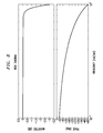
- FIG. 19 shows how the impedance level (R values) determines filter losses and filter peaking.
- FIG. 21 shows how bias current of the unity gain amplifiers controls filter losses and filter peaking.
- FIG. 22 shows how the amplifier's gain, G, controls filter losses and stability. G is controlled from the resistive load of the linearized pair. When G>1, the filter starts oscillating. The oscillation frequency is at peaking frequency (R>450 ⁇ ). It should be noted in general that peaking and losses should be avoided; values of R can cause instability and excessive peaking can cause oscillation. Note also that the value R (RVAL) is the absolute value of the tunable resistors in FIG. 12 .
- One or more embodiments provide a self-calibrated broadband tunable active Papoulis filter with only unity gain cells for multi-standard and/or multiband channel selection, workable at GHz frequencies (limited only by the gain-bandwidth product of the process), and having high linearity due to linearization techniques. Furthermore, one or more embodiments provide a configuration wherein the same filter topology is sued for the oscillation mode, allowing good on-chip matching with continuous calibration during operation (important for data communication). A digital PLL can be used for error signal and fine tuning, and only a small area is needed.
- an all-pole Papoulis filter is realized using unity-gain amplifiers without total feedback, OTAs or OP-AMPs, allowing larger bandwidths in excess of a few GHz.
- a significant building block for the filter is a unity-gain amplifier realized with a linearized pair and a buffer with local feedback.
- the filter can be tuned via a configuration with the filter and its replica working as an oscillator.
- the oscillator is active and one or more embodiments do not use only one time constant for matching to the main filter.
- the whole filter performs the oscillator function; this oscillator is not an LC oscillator.
- capacitor banks as well as MOS resistors having a coarse-fine tuning mechanism can be employed.
- the tuning mechanism relies on transforming the output of the oscillator in a digital signal using a Time-to-Digital Converter (TDC) and having its output frequency as a digital code.
- TDC Time-to-Digital Converter
- the crystal (X-Tal) reference is compared in the digital domain to the oscillation frequency of the filter-oscillator and the error signal is used for tuning the pass-band response.
- the filter has low-group delay due to Papoulis characteristic and due to large bandwidth of the unity-gain amplifiers. Continuous calibration (on-the-fly) is possible as the two functions (filter and oscillator) are separated.
- One or more instances can operate at large signal levels as the linearization of the first stage together with local feedback employed in the buffer allows operation with input differential signals (peak-to-peak) close to supply voltage (V pp, differential, in ⁇ VDD).
- the digital PLL or DPLL involved in the calibration process preferably has a small form factor as the loop filter is not integrated as a large capacitance.
- one or more embodiments realize an active Papoulis filter as an all-pole filter with very small group-delay; of significance is the use of high-linearity unity-gain cells with MOS transistors, capacitors and tunable resistors (realized as well with MOS transistors and poly resistors).
- the group-delays of such filters are better than Butterworth filters of the same order and can be used for communications purposes.
- This filter can be tuned coarsely by switching capacitors and finely by using resistors and MOS transistors.
- the result is a filter that can be used for multi-band, multi-standard wireless transceivers for WPAN and next generation WPAN (802.11.3.c) or UWB.
- the filter can have a self-calibrating mechanism based on a crystal reference provided by a PLL integrated on the same IC process.
- an exemplary filter includes N unity gain amplifiers (such as 1202 , 1204 , 1206 , 1208 ), N being at least two.
- Each of the unity gain amplifiers has a pair of differential input terminals and a pair of differential output terminals.
- the pair of differential output terminals of a last one of the N unity gain amplifiers are the filter differential output terminals (between which is V 0 ).
- a pair of filter differential input terminals (between which is Vi), and a first pair of variable resistances (e.g., R 4 plus FET with VDAC on gate) coupling the pair of filter differential input terminals to the pair of differential input terminals of a first one of the N unity gain amplifiers (e.g., 1202 ).
- a first pair of variable resistances e.g., R 4 plus FET with VDAC on gate
- N ⁇ 1 pairs of variable resistances couple the pairs of differential output terminals of each of the N unity gain amplifiers, other than the last one of the N unity gain amplifiers (e.g., 1208 ), to the pairs of differential input terminals of its downstream neighbor (that is, 1202 coupled to 1204 , 1204 coupled to 1206 ).
- N ⁇ 1 pairs of variable capacitances couple the pairs of differential input terminals of each of the N unity gain amplifiers, other than the last one of the N unity gain amplifiers, to the pairs of differential output terminals of its downstream neighbor; and a variable capacitance (e.g., C 1 , 0 /2 through C 1 ,m/2) couple the pair of differential input terminals of the last one of the N unity gain amplifiers (e.g., 1208 ) to each other.
- the N unity gain amplifiers each in turn comprise a linearized operational transconductance amplifier stage (for example, as seen in FIG. 13 ) coupled to a corresponding pair of the differential input terminals, and a unity gain buffer with feedback interconnected between the linearized operational transconductance amplifier stage and a corresponding pair of the differential output terminals, as seen in FIG. 15 .
- the unity gain buffer with feedback includes an additional pair of field effect transistors M 5 , M 14 having gates coupled to the drains of the second and third field effect transistors M 3 , M 1 and sources coupled to the corresponding pair of differential output terminals (+ in the case of M 5 ; ⁇ in the case of M 14 ). Also included is a loop arrangement configured to mirror the current from the current mirror in the additional pair of field effect transistors (refer, e.g., to discussion of loops around M 5 and M 14 in connection with above description of FIG. 15 ).
- variable resistances and variable capacitances can be achieved in a variety of ways; in a non-limiting example, as noted, the variable resistances are realized as fixed resistors coupled to metal oxide semiconductor field effect transistors configured to operate in triode mode, and the variable capacitances are realized as a hard-wired fixed capacitor (e.g., C 4 , 0 ; C 3 , 0 ; C 2 , 0 ; and C 1 , 0 /2) and one or more switched fixed capacitors (1 through m) in parallel thereto.
- a hard-wired fixed capacitor e.g., C 4 , 0 ; C 3 , 0 ; C 2 , 0 ; and C 1 , 0 /2
- a controller 1212 can be provided and can be operatively configured to provide band switching (for example, by switching the switched fixed capacitors) and to provide fine tuning (for example, by applying signals to the gates of the pairs of metal oxide semiconductor field effect transistors configured to operate in triode mode).
- the filter can be a Papoulis filter or other all-poles filter.
- the linearized operational transconductance amplifier stages each comprise a first field effect transistor M 3 interconnected between a supply voltage VDD and a current mirror and having a gate, a drain, and a source; a pair of variable resistances (each member of the pair formed by the four R/4 resistors) coupled to the supply voltage VDD; an additional pair of resistors Rx; and second and third field effect transistors M 1 and M 3 interconnected between the pair of variable resistances and the current mirror and each having a gate, a drain, and a source.
- the gates of the second and third field effect transistors are coupled to the gate of the first field effect transistor through the additional pair of resistors.
- the gates of the second and third field effect transistors comprise the corresponding pair of differential input terminals; the drains of the second and third field effect transistors are coupled to the corresponding pair of differential output terminals through the unity gain buffer with feedback, and the first field effect transistor having a device width at least twice a device width of the second and third field effect transistors (e.g., N ⁇ 2 as in FIG. 13 ).
- an exemplary filter includes N greater than unity gain amplifiers (e.g., 1602 , 1604 , 1606 , 1608 ), N being at least two.
- Each of the greater than unity gain amplifiers has a pair of differential input terminals and a pair of differential output terminals.
- a first pair of variable resistances e.g., R 4 plus FET with VDAC on gate
- the differential output terminals of the greater than unity gain amplifiers are coupled to the differential input terminals of their downstream neighbors through N ⁇ 1 pairs of variable resistances in a manner similar to the filter, and the differential input terminals of each greater than unity gain amplifier, other than the last one, is coupled to the differential output terminals of its downstream neighbor, through variable capacitances in a manner similar to the filter.
- a variable capacitance couples the differential input terminals of the last greater than unity gain amplifiers to each other, capacitances in a manner similar to the filter.
- the N greater than unity gain amplifiers each in turn comprise a linearized operational transconductance amplifier stage coupled to a corresponding pair of the differential input terminals; and a unity gain buffer with feedback interconnected between the linearized operational transconductance amplifier stage and a corresponding pair of the differential output terminals, as for the filter, except that the gain is greater than one (for example by adjusting the switched resistances shown in FIGS. 14 and 15 ).
- Control of the filter can be achieved as described above.
- an exemplary circuit includes a filter as described and an oscillator as described.
- the circuit can also include a control arrangement configured to compare the frequency of oscillation of the oscillator to a reference, and exert common control over the variable capacitances and resistances of the filter and oscillator, so as to match the frequency of oscillation of the oscillator to the reference and control bandwidth of the filter.
- the control arrangement is preferably operatively configured to switch the switched fixed capacitors to provide band switching and to apply signals to the gates of the pairs of metal oxide semiconductor field effect transistors configured to operate in triode mode to provide fine tuning.
- the filter and the oscillator are preferably realized on adjacent portions of an integrated circuit chip and are dimensionally identical within process limits of the process used to manufacture the integrated circuit chip.
- the pairs of variable resistances are adjusted to provide unity gain for the unity gain amplifiers and greater than unity gain for the greater than unity gain amplifiers.
- control arrangement comprises a time-to-digital converter 1873 coupled to the oscillator to sense the frequency of oscillation of the oscillator, a digital phase-locked loop 1875 coupled to the time-to-digital converter and configured to compare the reference to the frequency of oscillation of the oscillator sensed by the time-to-digital converter, and a controller 1212 coupled to the digital phase-locked loop and operatively configured to exert the common control in response to the comparison by the digital phase-locked loop.
- Integrated circuit chips in accordance with one or more embodiments of the invention can be distributed by the fabricator in raw wafer form (that is, as a single wafer that has multiple unpackaged chips), as a bare die, or in a packaged form.
- the chip is mounted in a single chip package (such as a plastic carrier, with leads that are affixed to a motherboard or other higher level carrier) or in a multichip package (such as a ceramic carrier that has either or both surface interconnections or buried interconnections).
- the chip is then integrated with other chips, discrete circuit elements, and/or other signal processing devices as part of either (a) an intermediate product, such as a motherboard, or (b) an end product.
- the end product can be any product that includes integrated circuit chips, such as, by way of example and not limitation, a communications circuit or the like.
- FIG. 23 shows a block diagram of an exemplary design flow 2300 used for example, in semiconductor IC logic design, simulation, test, layout, and manufacture.
- Design flow 2300 includes processes, machines and/or mechanisms for processing design structures or devices to generate logically or otherwise functionally equivalent representations of the design structures and/or devices described above and shown in FIGS. 1 , 2 , and 12 - 18 .
- the design structures processed and/or generated by design flow 2300 may be encoded on machine-readable transmission or storage media to include data and/or instructions that when executed or otherwise processed on a data processing system generate a logically, structurally, mechanically, or otherwise functionally equivalent representation of hardware components, circuits, devices, or systems.
- Machines include, but are not limited to, any machine used in an IC design process, such as designing, manufacturing, or simulating a circuit, component, device, or system.
- machines may include: lithography machines, machines and/or equipment for generating masks (e.g. e-beam writers), computers or equipment for simulating design structures, any apparatus used in the manufacturing or test process, or any machines for programming functionally equivalent representations of the design structures into any medium(e.g. a machine for programming a programmable gate array).
- Design flow 2300 may vary depending on the type of representation being designed.
- a design flow 2300 for building an application specific IC may differ from a design flow 2300 for designing a standard component or from a design flow 2300 for instantiating the design into a programmable array, for example a programmable gate array (PGA) or a field programmable gate array (FPGA) offered by Altera® Inc. or Xilinx® Inc.
- FIG. 23 illustrates multiple such design structures including an input design structure 2320 that is preferably processed by a design process 2310 .
- Design structure 2320 may be a logical simulation design structure generated and processed by design process 2310 to produce a logically equivalent functional representation of a hardware device.
- Design structure 2320 may also or alternatively comprise data and/or program instructions that when processed by design process 2310 , generate a functional representation of the physical structure of a hardware device. Whether representing functional and/or structural design features, design structure 2320 may be generated using electronic computer-aided design (ECAD) such as implemented by a core developer/designer. When encoded on a machine-readable data transmission, gate array, or storage medium, design structure 2320 may be accessed and processed by one or more hardware and/or software modules within design process 2310 to simulate or otherwise functionally represent an electronic component, circuit, electronic or logic module, apparatus, device, or system such as those shown in FIGS. 1 , 2 , and 12 - 18 .
- ECAD electronic computer-aided design
- design structure 2320 may comprise files or other data structures including human and/or machine-readable source code, compiled structures, and computer-executable code structures that when processed by a design or simulation data processing system, functionally simulate or otherwise represent circuits or other levels of hardware logic design.
- data structures may include hardware-description language(HDL) design entities or other data structures conforming to and/or compatible with lower-level HDL design languages such as Verilog and VHDL, and/or higher level design languages such as C or C++.
- Design process 2310 preferably employs and incorporates hardware and/or software modules for synthesizing, translating, or otherwise processing a design/simulation functional equivalent of the components, circuits, devices, or logic structures shown in FIGS.
- netlist 2380 may contain design structures such as design structure 2320 .
- Netlist 2380 may comprise, for example, compiled or otherwise processed data structures representing a list of wires, discrete components, logic gates, control circuits, I/O devices, models, etc. that describes the connections to other elements and circuits in an integrated circuit design.
- Netlist 2380 may be synthesized using an iterative process in which netlist 2380 is resynthesized one or more times depending on design specifications and parameters for the device. As with other design structure types described herein, netlist 2380 may be recorded on a machine-readable data storage medium or programmed into a programmable gate array.
- the medium may be a non-volatile storage medium such as a magnetic or optical disk drive, a programmable gate array, a compact flash, or other flash memory. Additionally, or in the alternative, the medium may be a system or cache memory, buffer space, or electrically or optically conductive devices and materials on which data packets may be transmitted and intermediately stored via the Internet, or other networking suitable means.
- Design process 2310 may include hardware and software modules for processing a variety of input data structure types including netlist 2380 .
- Such data structure types may reside, for example, within library elements 2330 and include a set of commonly used elements, circuits, and devices, including models, layouts, and symbolic representations, for a given manufacturing technology(e.g., different technology nodes, 32 nm, 45 nm, 90 nm, etc.).
- the data structure types may further include design specifications 2340 , characterization data 2350 , verification data 2360 , design rules 2370 , and test data files 2385 which may include input test patterns, output test results, and other testing information.
- Design process 2310 may further include, for example, standard mechanical design processes such as stress analysis, thermal analysis, mechanical event simulation, process simulation for operations such as casting, molding, and die press forming, etc.
- Design process 2310 may also include modules for performing standard circuit design processes such as timing analysis, verification, design rule checking, place and route operations, etc.
- Design process 2310 employs and incorporates logic and physical design tools such as HDL compilers and simulation model build tools to process design structure 2320 together with some or all of the depicted supporting data structures along with any additional mechanical design or data(if applicable), to generate a second design structure 2390 .
- Design structure 2390 resides on a storage medium or programmable gate array in a data format used for the exchange of data of mechanical devices and structures (e.g.
- design structure 2390 preferably comprises one or more files, data structures, or other computer-encoded data or instructions that reside on transmission or data storage media and that when processed by an ECAD system generate a logically or otherwise functionally equivalent form of one or more of the embodiments of the invention shown in FIGS. 1 , 2 , and 12 - 18 .
- design structure 2390 may comprise a compiled, executable HDL simulation model that functionally simulates the devices shown in FIGS. 1 , 2 , and 12 - 18 .
- Design structure 2390 may also employ a data format used for the exchange of layout data of integrated circuits and/or symbolic data format (e.g. information stored in a GDSII (GDS2), GL1, OASIS, map files, or any other suitable format for storing such design data structures).
- Design structure 2390 may comprise information such as, for example, symbolic data, map files, test files, design content files, manufacturing data, layout parameters, wires, levels of metal, vias, shapes, data for routing through the manufacturing line, and any other data required by a manufacturer or other designer/developer to produce a device or structure as described above and shown in FIGS. 1 , 2 , and 12 - 18 .
- Design structure 2390 may then proceed to a stage 2395 where, for example, design structure 2390 : proceeds to tape-out, is released to manufacturing, is released to a mask house, is sent to another design house, is sent back to the customer, etc.
Abstract
Description
-
- can be implemented in modern technologies with high bandwidths (greater than 1 GHz) suitable for use in 60 GHz communications systems
- unlike op-amp based filters (MOSFET plus capacitance), do not have large gain requirements to create virtual ground at the input
- recue or eliminate linearity problems with OTA-C or Gm-C filters
- avoid limits on achievable Q due to second pole of OTA based integrator
- achieve sharp transition bands and large stop-band rejection
- low power consumption, especially compared to bi-quads with OTA-C filters
- less group-delay than filters with poles and zeroes; low group delay is important for data communications
- can operate at low voltages and provides a tunable pass-band characteristic
- can achieve self calibration and continuous operation
- can provide a multiband solution
- less chip area than L and C solutions
Claims (13)
Priority Applications (2)
| Application Number | Priority Date | Filing Date | Title |
|---|---|---|---|
| US13/010,249 US8344795B2 (en) | 2011-01-20 | 2011-01-20 | Self-calibrated, broadband, tunable, active filter with unity gain cells for multi-standard and/or multiband channel selection |
| US13/648,799 US8487693B2 (en) | 2011-01-20 | 2012-10-10 | Self calibrated, broadband, tunable, active oscillator with unity gain cells for multi-standard and/or multiband channel selection |
Applications Claiming Priority (1)
| Application Number | Priority Date | Filing Date | Title |
|---|---|---|---|
| US13/010,249 US8344795B2 (en) | 2011-01-20 | 2011-01-20 | Self-calibrated, broadband, tunable, active filter with unity gain cells for multi-standard and/or multiband channel selection |
Related Child Applications (1)
| Application Number | Title | Priority Date | Filing Date |
|---|---|---|---|
| US13/648,799 Division US8487693B2 (en) | 2011-01-20 | 2012-10-10 | Self calibrated, broadband, tunable, active oscillator with unity gain cells for multi-standard and/or multiband channel selection |
Publications (2)
| Publication Number | Publication Date |
|---|---|
| US20120188006A1 US20120188006A1 (en) | 2012-07-26 |
| US8344795B2 true US8344795B2 (en) | 2013-01-01 |
Family
ID=46543740
Family Applications (2)
| Application Number | Title | Priority Date | Filing Date |
|---|---|---|---|
| US13/010,249 Expired - Fee Related US8344795B2 (en) | 2011-01-20 | 2011-01-20 | Self-calibrated, broadband, tunable, active filter with unity gain cells for multi-standard and/or multiband channel selection |
| US13/648,799 Expired - Fee Related US8487693B2 (en) | 2011-01-20 | 2012-10-10 | Self calibrated, broadband, tunable, active oscillator with unity gain cells for multi-standard and/or multiband channel selection |
Family Applications After (1)
| Application Number | Title | Priority Date | Filing Date |
|---|---|---|---|
| US13/648,799 Expired - Fee Related US8487693B2 (en) | 2011-01-20 | 2012-10-10 | Self calibrated, broadband, tunable, active oscillator with unity gain cells for multi-standard and/or multiband channel selection |
Country Status (1)
| Country | Link |
|---|---|
| US (2) | US8344795B2 (en) |
Cited By (1)
| Publication number | Priority date | Publication date | Assignee | Title |
|---|---|---|---|---|
| US20170179940A1 (en) * | 2014-04-14 | 2017-06-22 | China Electronic Technology Corporation, 24Th Research Institute | Track and hold circuit |
Families Citing this family (4)
| Publication number | Priority date | Publication date | Assignee | Title |
|---|---|---|---|---|
| US8889475B1 (en) * | 2013-05-30 | 2014-11-18 | International Business Machines Corporation | Self-aligned bottom-gated graphene devices |
| US9444468B2 (en) | 2013-12-23 | 2016-09-13 | Infineon Technologies Ag | Oscillator devices and methods |
| US10608601B2 (en) | 2017-05-31 | 2020-03-31 | Qualcomm Incorporated | Active biquad filter with oscillator circuit |
| CN116455340B (en) * | 2023-06-16 | 2023-08-18 | 广州市声讯电子科技股份有限公司 | Loudspeaker audio gain control system and method |
Citations (48)
| Publication number | Priority date | Publication date | Assignee | Title |
|---|---|---|---|---|
| US3946328A (en) | 1975-01-27 | 1976-03-23 | Northern Electric Company, Limited | Functionally tunable active filter |
| US4095218A (en) | 1976-08-30 | 1978-06-13 | International Business Machines Corporation | Hybrid pulse width-pulse rate digital-to-analog converter method and apparatus |
| US4862121A (en) * | 1987-08-13 | 1989-08-29 | Texas Instruments Incorporated | Switched capacitor filter |
| US4952891A (en) | 1988-10-21 | 1990-08-28 | U.S. Philips Corporation | Filter circuit with automatic tuning |
| US5036219A (en) | 1989-05-31 | 1991-07-30 | Harris Corporation | Precise, high speed CMOS track (sample)/hold circuits |
| US5298801A (en) | 1991-09-11 | 1994-03-29 | U.S. Philips Corporation | Track-and-hold circuit |
| US5389929A (en) | 1994-02-03 | 1995-02-14 | Raytheon Company | Two-step subranging analog-to-digital converter |
| US5495200A (en) * | 1993-04-06 | 1996-02-27 | Analog Devices, Inc. | Double sampled biquad switched capacitor filter |
| US5517141A (en) | 1993-11-05 | 1996-05-14 | Motorola, Inc. | Differential high speed track and hold amplifier |
| US5673047A (en) | 1995-06-06 | 1997-09-30 | Analog Devices, Inc. | Gain-compensating differential reference circuit |
| US5736878A (en) | 1996-06-21 | 1998-04-07 | Delco Electronics Corporaiton | Low cost, high speed track and hold circuit |
| US6011431A (en) | 1994-11-23 | 2000-01-04 | Analog Devices, Inc. | Automatically tracking multiple-pole active filter |
| US6037891A (en) | 1998-02-23 | 2000-03-14 | Motorola, Inc. | Low power serial analog-to-digital converter |
| US6094093A (en) | 1997-01-22 | 2000-07-25 | Lucent Technologies Inc. | Low-voltage input buffer |
| US6307443B1 (en) | 1999-09-24 | 2001-10-23 | Agere Systems Guardian Corp. | Bandpass filters with automatic tuning adjustment |
| US6373332B2 (en) * | 1999-12-01 | 2002-04-16 | General Research Of Electronics, Inc. | Biquad notch filter |
| US6480133B2 (en) | 2000-01-21 | 2002-11-12 | Sanyo Electric Co., Ltd. | Low-power analog-to-digital converter |
| US6657488B1 (en) | 2001-07-03 | 2003-12-02 | Silicon Laboratories, Inc. | Offset correction and slicing level adjustment for amplifier circuits |
| US6731155B2 (en) | 2002-02-13 | 2004-05-04 | Intersil Americas Inc | Track and hold with dual pump circuit |
| WO2004066487A2 (en) | 2002-12-18 | 2004-08-05 | Bae Systems Information And Electronic Systems Integration Inc. | High speed track and hold amplifier for direct digital down-conversion |
| US6778023B2 (en) | 2001-07-31 | 2004-08-17 | Nokia Corporation | Tunable filter and method of tuning a filter |
| US6798726B2 (en) | 2000-08-02 | 2004-09-28 | Koninklijke Philips Electronics N.V. | Data decoding |
| US6803813B1 (en) | 2003-04-22 | 2004-10-12 | National Semiconductor Corporation | Time constant-based calibration circuit for active filters |
| US6831584B2 (en) | 2002-09-03 | 2004-12-14 | Broadcom Corporation | High-speed low-distortion analog-to digital converter |
| WO2005013284A1 (en) | 2003-08-04 | 2005-02-10 | Koninklijke Philips Electronics N.V. | Track-and-hold circuit |
| US6930565B1 (en) | 2003-04-28 | 2005-08-16 | Adam S. Vishinsky | Fully integrated automatically-tuned RF and IF active bandpass filters |
| US20060001455A1 (en) | 2004-07-01 | 2006-01-05 | Bernd Wuppermann | Circuit and method for performing track and hold operations |
| US20060049857A1 (en) | 2004-09-09 | 2006-03-09 | The Regents Of The University Of California | Switch linearized track and hold circuit for switch linearization |
| US20060125531A1 (en) | 2004-12-13 | 2006-06-15 | Allegro Microsystems, Inc. | Track-and-hold peak detector circuit |
| US7075364B2 (en) * | 2004-08-17 | 2006-07-11 | Qualcomm Incorporated | Active-RC filter with compensation to reduce Q enhancement |
| US20060152251A1 (en) | 2005-01-12 | 2006-07-13 | Setterberg Brian D | High dynamic range current-mode track-and-hold circuit |
| US7136000B1 (en) | 2005-06-17 | 2006-11-14 | National Semiconductor Corporation | Selective offset adjustment of a track and hold circuit |
| US7148828B2 (en) | 2005-05-03 | 2006-12-12 | Agilent Technologies, Inc. | System and method for timing calibration of time-interleaved data converters |
| US20070008030A1 (en) | 2003-09-05 | 2007-01-11 | Kasperkovitz Woldfietrich G | Control system for programmable filters |
| US20070152863A1 (en) | 2005-12-13 | 2007-07-05 | Broadcom Corporation | Digital calibration loop for an analog to digital converter |
| US20080150772A1 (en) | 2006-12-21 | 2008-06-26 | Broadcom Corporation | Apparatus and method for analog-to-digital converter calibration |
| US7400212B1 (en) | 2005-06-07 | 2008-07-15 | Vishinsky Adam S | Self-tuned active bandpass filters |
| US7425863B2 (en) * | 2005-12-13 | 2008-09-16 | Broadcom Corporation | Tuneable filters using operational amplifiers |
| US20090015329A1 (en) | 2004-09-20 | 2009-01-15 | Shouri Chatterjee | Low Voltage Track and Hold Circuits |
| US20090039923A1 (en) | 2007-08-08 | 2009-02-12 | Texas Instruments Incorporated | Track-and-hold circuit with low distortion |
| US7492242B2 (en) | 2005-03-18 | 2009-02-17 | Stmicroelectronics S.A. | Integrable tunable filter circuit comprising a set of BAW resonators |
| US20090066555A1 (en) | 2006-01-31 | 2009-03-12 | Interuniversitair Microelektronica Centrum(Imec) | A/D Converter Comprising a Voltage Comparator Device |
| US20090072868A1 (en) | 2007-09-17 | 2009-03-19 | Samsung Electronics Co., Ltd. | Wideband track-and-hold amplifier |
| WO2009034518A2 (en) | 2007-09-12 | 2009-03-19 | Nxp B.V. | Time-interleaved track and hold |
| US7528752B1 (en) | 2007-04-13 | 2009-05-05 | Link—A—Media Devices Corporation | Offset compensation scheme using a DAC |
| US7545235B2 (en) | 2005-12-07 | 2009-06-09 | Mansour Raafat R | Dielectric resonator filter assemblies and methods |
| US20090278625A1 (en) | 2008-05-08 | 2009-11-12 | Hong Fu Jin Precision Industry (Shenzhen) Co., Ltd. | Broadband filter |
| US20100022215A1 (en) | 2008-07-28 | 2010-01-28 | Freescale Semiconductor, Inc. | Baseband filters for use in wireless communication devices |
Family Cites Families (2)
| Publication number | Priority date | Publication date | Assignee | Title |
|---|---|---|---|---|
| US5625317A (en) * | 1994-08-08 | 1997-04-29 | Texas Instruments Incorporated | Tuning method for integrated continuous-time filters |
| US7474160B2 (en) * | 2005-05-25 | 2009-01-06 | Qualcomm Incorporated | Systems and methods for calibrating a filter |
-
2011
- 2011-01-20 US US13/010,249 patent/US8344795B2/en not_active Expired - Fee Related
-
2012
- 2012-10-10 US US13/648,799 patent/US8487693B2/en not_active Expired - Fee Related
Patent Citations (50)
| Publication number | Priority date | Publication date | Assignee | Title |
|---|---|---|---|---|
| US3946328A (en) | 1975-01-27 | 1976-03-23 | Northern Electric Company, Limited | Functionally tunable active filter |
| US4095218A (en) | 1976-08-30 | 1978-06-13 | International Business Machines Corporation | Hybrid pulse width-pulse rate digital-to-analog converter method and apparatus |
| US4862121A (en) * | 1987-08-13 | 1989-08-29 | Texas Instruments Incorporated | Switched capacitor filter |
| US4952891A (en) | 1988-10-21 | 1990-08-28 | U.S. Philips Corporation | Filter circuit with automatic tuning |
| US5036219A (en) | 1989-05-31 | 1991-07-30 | Harris Corporation | Precise, high speed CMOS track (sample)/hold circuits |
| US5298801A (en) | 1991-09-11 | 1994-03-29 | U.S. Philips Corporation | Track-and-hold circuit |
| US5495200A (en) * | 1993-04-06 | 1996-02-27 | Analog Devices, Inc. | Double sampled biquad switched capacitor filter |
| US5517141A (en) | 1993-11-05 | 1996-05-14 | Motorola, Inc. | Differential high speed track and hold amplifier |
| US5389929A (en) | 1994-02-03 | 1995-02-14 | Raytheon Company | Two-step subranging analog-to-digital converter |
| US6011431A (en) | 1994-11-23 | 2000-01-04 | Analog Devices, Inc. | Automatically tracking multiple-pole active filter |
| US5673047A (en) | 1995-06-06 | 1997-09-30 | Analog Devices, Inc. | Gain-compensating differential reference circuit |
| US5736878A (en) | 1996-06-21 | 1998-04-07 | Delco Electronics Corporaiton | Low cost, high speed track and hold circuit |
| US6094093A (en) | 1997-01-22 | 2000-07-25 | Lucent Technologies Inc. | Low-voltage input buffer |
| US6037891A (en) | 1998-02-23 | 2000-03-14 | Motorola, Inc. | Low power serial analog-to-digital converter |
| US6307443B1 (en) | 1999-09-24 | 2001-10-23 | Agere Systems Guardian Corp. | Bandpass filters with automatic tuning adjustment |
| US6373332B2 (en) * | 1999-12-01 | 2002-04-16 | General Research Of Electronics, Inc. | Biquad notch filter |
| US6480133B2 (en) | 2000-01-21 | 2002-11-12 | Sanyo Electric Co., Ltd. | Low-power analog-to-digital converter |
| US6798726B2 (en) | 2000-08-02 | 2004-09-28 | Koninklijke Philips Electronics N.V. | Data decoding |
| US6657488B1 (en) | 2001-07-03 | 2003-12-02 | Silicon Laboratories, Inc. | Offset correction and slicing level adjustment for amplifier circuits |
| US6778023B2 (en) | 2001-07-31 | 2004-08-17 | Nokia Corporation | Tunable filter and method of tuning a filter |
| US6731155B2 (en) | 2002-02-13 | 2004-05-04 | Intersil Americas Inc | Track and hold with dual pump circuit |
| US6831584B2 (en) | 2002-09-03 | 2004-12-14 | Broadcom Corporation | High-speed low-distortion analog-to digital converter |
| WO2004066487A2 (en) | 2002-12-18 | 2004-08-05 | Bae Systems Information And Electronic Systems Integration Inc. | High speed track and hold amplifier for direct digital down-conversion |
| US6803813B1 (en) | 2003-04-22 | 2004-10-12 | National Semiconductor Corporation | Time constant-based calibration circuit for active filters |
| US6930565B1 (en) | 2003-04-28 | 2005-08-16 | Adam S. Vishinsky | Fully integrated automatically-tuned RF and IF active bandpass filters |
| US20060192546A1 (en) | 2003-08-04 | 2006-08-31 | Koninklijke Philips Electronics N.V. | Track-and-hold circuit |
| WO2005013284A1 (en) | 2003-08-04 | 2005-02-10 | Koninklijke Philips Electronics N.V. | Track-and-hold circuit |
| US20070008030A1 (en) | 2003-09-05 | 2007-01-11 | Kasperkovitz Woldfietrich G | Control system for programmable filters |
| US20060001455A1 (en) | 2004-07-01 | 2006-01-05 | Bernd Wuppermann | Circuit and method for performing track and hold operations |
| US7154306B2 (en) | 2004-07-01 | 2006-12-26 | Agilent Technologies, Inc. | Circuit and method for performing track and hold operations |
| US7075364B2 (en) * | 2004-08-17 | 2006-07-11 | Qualcomm Incorporated | Active-RC filter with compensation to reduce Q enhancement |
| US20060049857A1 (en) | 2004-09-09 | 2006-03-09 | The Regents Of The University Of California | Switch linearized track and hold circuit for switch linearization |
| US20090015329A1 (en) | 2004-09-20 | 2009-01-15 | Shouri Chatterjee | Low Voltage Track and Hold Circuits |
| US20060125531A1 (en) | 2004-12-13 | 2006-06-15 | Allegro Microsystems, Inc. | Track-and-hold peak detector circuit |
| US20060152251A1 (en) | 2005-01-12 | 2006-07-13 | Setterberg Brian D | High dynamic range current-mode track-and-hold circuit |
| US7492242B2 (en) | 2005-03-18 | 2009-02-17 | Stmicroelectronics S.A. | Integrable tunable filter circuit comprising a set of BAW resonators |
| US7148828B2 (en) | 2005-05-03 | 2006-12-12 | Agilent Technologies, Inc. | System and method for timing calibration of time-interleaved data converters |
| US7400212B1 (en) | 2005-06-07 | 2008-07-15 | Vishinsky Adam S | Self-tuned active bandpass filters |
| US7136000B1 (en) | 2005-06-17 | 2006-11-14 | National Semiconductor Corporation | Selective offset adjustment of a track and hold circuit |
| US7545235B2 (en) | 2005-12-07 | 2009-06-09 | Mansour Raafat R | Dielectric resonator filter assemblies and methods |
| US7425863B2 (en) * | 2005-12-13 | 2008-09-16 | Broadcom Corporation | Tuneable filters using operational amplifiers |
| US20070152863A1 (en) | 2005-12-13 | 2007-07-05 | Broadcom Corporation | Digital calibration loop for an analog to digital converter |
| US20090066555A1 (en) | 2006-01-31 | 2009-03-12 | Interuniversitair Microelektronica Centrum(Imec) | A/D Converter Comprising a Voltage Comparator Device |
| US20080150772A1 (en) | 2006-12-21 | 2008-06-26 | Broadcom Corporation | Apparatus and method for analog-to-digital converter calibration |
| US7528752B1 (en) | 2007-04-13 | 2009-05-05 | Link—A—Media Devices Corporation | Offset compensation scheme using a DAC |
| US20090039923A1 (en) | 2007-08-08 | 2009-02-12 | Texas Instruments Incorporated | Track-and-hold circuit with low distortion |
| WO2009034518A2 (en) | 2007-09-12 | 2009-03-19 | Nxp B.V. | Time-interleaved track and hold |
| US20090072868A1 (en) | 2007-09-17 | 2009-03-19 | Samsung Electronics Co., Ltd. | Wideband track-and-hold amplifier |
| US20090278625A1 (en) | 2008-05-08 | 2009-11-12 | Hong Fu Jin Precision Industry (Shenzhen) Co., Ltd. | Broadband filter |
| US20100022215A1 (en) | 2008-07-28 | 2010-01-28 | Freescale Semiconductor, Inc. | Baseband filters for use in wireless communication devices |
Non-Patent Citations (16)
| Title |
|---|
| A. Papoulis, "On Monotonic Response Filters," Proceedings of the IRE, Feb. 1959, pp. 332-333, vol. 47. |
| A. Papoulis, "Optimum Filters with Monotonic Response," Proceedings of the IRE, Mar. 1958, pp. 606-609, vol. 46, No. 3. |
| A.M. Abo et al., "A 1.5-V, 10-Bit, 14.3-MS/s CMOS Pipeline Analog-to-Digital Converter," IEEE Journal of Solid-State Circuits, May 1999, pp. 599-606, vol. 34, No. 5. |
| Andrew N. Karanicolas, "A 2.7-V 300-MS/s Track-and-Hold Amplifier," IEEE Journal of Solid-State Circuits, Dec. 1997, pp. 1961-1967, vol. 32, No. 12. |
| H. Pan et al., "A 3.3-V 12-b 50-MS/s A/D Converter in 0.6-mum CMOS with Over 80-dB SFDR," IEEE Journal of Solid-State Circuits, Dec. 2000, pp. 1769-1780, vol. 35, No. 12. |
| H. Pan et al., "A 3.3-V 12-b 50-MS/s A/D Converter in 0.6-μm CMOS with Over 80-dB SFDR," IEEE Journal of Solid-State Circuits, Dec. 2000, pp. 1769-1780, vol. 35, No. 12. |
| J. Steensgaard, "Bootstrapped Low-Voltage Analog Switches," IEEE International Symposium on Circuits and Systems, Jul. 1999, pp. 29-32, vol. 2. |
| K.Y. Leung et al., "A Dual Low Power ½ LSB INL 16b/1 Msample/s SAR A/D Converter with On-Chip Microcontroller," IEEE Asian Solid-State Circuits Conference, Nov. 2006, pp. 51-54. |
| M. Dessouky et al., "Very Low-Voltage Digital-Audio DeltaSigma Modulator with 88-dB Dynamic Range Using Local Switch Bootstrapping," Mar. 2001, pp. 349-355, vol. 36, No. 3. |
| M. Dessouky et al., "Very Low-Voltage Digital-Audio ΔΣ Modulator with 88-dB Dynamic Range Using Local Switch Bootstrapping," Mar. 2001, pp. 349-355, vol. 36, No. 3. |
| M. Wang et al., "Low-Power 4-b 2.5-GSPS Pipelined Flash Analog-to-Digital Converter in 130-nm CMOS," IEEE Transactions on Instrumentation and Measurement, Jun. 2007, pp. 1064-1073, vol. 56, No. 3. |
| M.P. Flynn et al., "Digital Calibration Incorporating Redundancy of Flash ADCs," IEEE Transactions on Circuits and Systems-II: Analog and Digital Signal Processing, May 2003, pp. 205-213, vol. 50, No. 5. |
| Ron Tipton, "All About Electronically-Tunable Active Filters," Poptronics, Aug. 2000, pp. 42-50. |
| S. Shahramian et al., "A 40-G samples/sec Track & Hold Amplifier in 0.18 mum SiGe BiCMOS Technology," IEEE Compound Semiconductor Integrated Circuit Symposium, Oct.-Nov. 2005, pp. 101-104. |
| S. Shahramian et al., "A 40-G samples/sec Track & Hold Amplifier in 0.18 μm SiGe BiCMOS Technology," IEEE Compound Semiconductor Integrated Circuit Symposium, Oct.-Nov. 2005, pp. 101-104. |
| U.S. Appl. No. 13/010,285, filed in the name of M.A.T. Sanduleanu et al. on Jan. 20, 2011 and entitled "Track and Hold Amplifiers and Digital Calibration for Analog-to-Digital Converters." |
Cited By (2)
| Publication number | Priority date | Publication date | Assignee | Title |
|---|---|---|---|---|
| US20170179940A1 (en) * | 2014-04-14 | 2017-06-22 | China Electronic Technology Corporation, 24Th Research Institute | Track and hold circuit |
| US10128830B2 (en) * | 2014-04-14 | 2018-11-13 | China Electronic Technology Corporation, 24Th Research Institute | Track and hold circuit |
Also Published As
| Publication number | Publication date |
|---|---|
| US8487693B2 (en) | 2013-07-16 |
| US20120188006A1 (en) | 2012-07-26 |
| US20130033333A1 (en) | 2013-02-07 |
Similar Documents
| Publication | Publication Date | Title |
|---|---|---|
| US8487693B2 (en) | Self calibrated, broadband, tunable, active oscillator with unity gain cells for multi-standard and/or multiband channel selection | |
| US7180364B2 (en) | Filter apparatus including slave gm-C filter with frequency characteristics automatically tuned by master circuit | |
| JP4481590B2 (en) | Active inductance circuit and differential amplifier circuit | |
| US7492242B2 (en) | Integrable tunable filter circuit comprising a set of BAW resonators | |
| EP0851578B1 (en) | Filter circuit | |
| US5621355A (en) | Sampled data-biasing of continuous time integrated circuit | |
| Xiao et al. | A radio-frequency CMOS active inductor and its application in designing high-Q filters | |
| Weng et al. | An ω 0-Q tunable CMOS active inductor for RF bandpass filters | |
| Sunca et al. | A wide tunable bandpass filter design based on CMOS active inductor | |
| US9124251B2 (en) | Two stage source-follower based filter | |
| Manjula et al. | Performance analysis of a low power low noise tunable band pass filter for multiband RF front end | |
| JP4086371B2 (en) | Semiconductor amplifier circuit | |
| JP4768186B2 (en) | Phase compensated impedance converter | |
| KR100776664B1 (en) | Ultra-wideband active differential signal low pass filter | |
| Zheng et al. | A microwave OTA using a feedforward-regulated cascode topology | |
| JP2002118443A (en) | Filter circuit | |
| Pantoli et al. | RF active circuit simulating a floating inductance | |
| Otin et al. | A 40–200 MHz programmable 4 th-order G m-C filter with auto-tuning system | |
| Córdova et al. | A 2.3-GHz CMOS high-Q bandpass filter design using an active inductor | |
| Ramirez-Angulo et al. | Large f/sub 0/Q second order filters using multiple output OTAs | |
| JP2007519366A (en) | Integrated variable frequency filter for wideband tuners. | |
| Hammadi et al. | Compact tunable bandpass filter for RF and microwave applications | |
| Mehrmanesh et al. | An ultra low-voltage Gm-C filter for video applications | |
| Li et al. | CMOS high-linear wide-dynamic range RF on-chip filters using Q-enhanced LC filters | |
| Thirugnanam et al. | Design of a tunable fully differential GHz range Gm-C lowpass filter in 0.18/spl mu/m CMOS for DS-CDMA UWB transceivers |
Legal Events
| Date | Code | Title | Description |
|---|---|---|---|
| AS | Assignment |
Owner name: MEDIATEK, TAIWAN Free format text: ASSIGNMENT OF ASSIGNORS INTEREST;ASSIGNOR:CHEN, PING-YU;REEL/FRAME:026116/0821 Effective date: 20110406 Owner name: INTERNATIONAL BUSINESS MACHINES CORPORATION, NEW Y Free format text: ASSIGNMENT OF ASSIGNORS INTEREST;ASSIGNOR:SANDULEANU, MIHAI;REEL/FRAME:026116/0694 Effective date: 20110408 |
|
| STCF | Information on status: patent grant |
Free format text: PATENTED CASE |
|
| AS | Assignment |
Owner name: GLOBALFOUNDRIES U.S. 2 LLC, NEW YORK Free format text: ASSIGNMENT OF ASSIGNORS INTEREST;ASSIGNOR:INTERNATIONAL BUSINESS MACHINES CORPORATION;REEL/FRAME:036550/0001 Effective date: 20150629 |
|
| AS | Assignment |
Owner name: GLOBALFOUNDRIES INC., CAYMAN ISLANDS Free format text: ASSIGNMENT OF ASSIGNORS INTEREST;ASSIGNORS:GLOBALFOUNDRIES U.S. 2 LLC;GLOBALFOUNDRIES U.S. INC.;REEL/FRAME:036779/0001 Effective date: 20150910 |
|
| FPAY | Fee payment |
Year of fee payment: 4 |
|
| AS | Assignment |
Owner name: WILMINGTON TRUST, NATIONAL ASSOCIATION, DELAWARE Free format text: SECURITY AGREEMENT;ASSIGNOR:GLOBALFOUNDRIES INC.;REEL/FRAME:049490/0001 Effective date: 20181127 |
|
| FEPP | Fee payment procedure |
Free format text: MAINTENANCE FEE REMINDER MAILED (ORIGINAL EVENT CODE: REM.); ENTITY STATUS OF PATENT OWNER: LARGE ENTITY |
|
| AS | Assignment |
Owner name: GLOBALFOUNDRIES INC., CAYMAN ISLANDS Free format text: RELEASE BY SECURED PARTY;ASSIGNOR:WILMINGTON TRUST, NATIONAL ASSOCIATION;REEL/FRAME:054636/0001 Effective date: 20201117 |
|
| LAPS | Lapse for failure to pay maintenance fees |
Free format text: PATENT EXPIRED FOR FAILURE TO PAY MAINTENANCE FEES (ORIGINAL EVENT CODE: EXP.); ENTITY STATUS OF PATENT OWNER: LARGE ENTITY |
|
| STCH | Information on status: patent discontinuation |
Free format text: PATENT EXPIRED DUE TO NONPAYMENT OF MAINTENANCE FEES UNDER 37 CFR 1.362 |
|
| FP | Lapsed due to failure to pay maintenance fee |
Effective date: 20210101 |
|
| AS | Assignment |
Owner name: GLOBALFOUNDRIES U.S. INC., NEW YORK Free format text: RELEASE BY SECURED PARTY;ASSIGNOR:WILMINGTON TRUST, NATIONAL ASSOCIATION;REEL/FRAME:056987/0001 Effective date: 20201117 |