US8345497B2 - Internal bypassing of memory array devices - Google Patents
Internal bypassing of memory array devices Download PDFInfo
- Publication number
- US8345497B2 US8345497B2 US12/822,058 US82205810A US8345497B2 US 8345497 B2 US8345497 B2 US 8345497B2 US 82205810 A US82205810 A US 82205810A US 8345497 B2 US8345497 B2 US 8345497B2
- Authority
- US
- United States
- Prior art keywords
- logic
- output node
- memory
- read
- during
- Prior art date
- Legal status (The legal status is an assumption and is not a legal conclusion. Google has not performed a legal analysis and makes no representation as to the accuracy of the status listed.)
- Expired - Fee Related, expires
Links
Images


Classifications
-
- G—PHYSICS
- G11—INFORMATION STORAGE
- G11C—STATIC STORES
- G11C16/00—Erasable programmable read-only memories
- G11C16/02—Erasable programmable read-only memories electrically programmable
-
- G—PHYSICS
- G11—INFORMATION STORAGE
- G11C—STATIC STORES
- G11C11/00—Digital stores characterised by the use of particular electric or magnetic storage elements; Storage elements therefor
- G11C11/21—Digital stores characterised by the use of particular electric or magnetic storage elements; Storage elements therefor using electric elements
- G11C11/34—Digital stores characterised by the use of particular electric or magnetic storage elements; Storage elements therefor using electric elements using semiconductor devices
- G11C11/40—Digital stores characterised by the use of particular electric or magnetic storage elements; Storage elements therefor using electric elements using semiconductor devices using transistors
- G11C11/41—Digital stores characterised by the use of particular electric or magnetic storage elements; Storage elements therefor using electric elements using semiconductor devices using transistors forming static cells with positive feedback, i.e. cells not needing refreshing or charge regeneration, e.g. bistable multivibrator or Schmitt trigger
- G11C11/413—Auxiliary circuits, e.g. for addressing, decoding, driving, writing, sensing, timing or power reduction
-
- G—PHYSICS
- G11—INFORMATION STORAGE
- G11C—STATIC STORES
- G11C7/00—Arrangements for writing information into, or reading information out from, a digital store
- G11C7/10—Input/output [I/O] data interface arrangements, e.g. I/O data control circuits, I/O data buffers
- G11C7/1048—Data bus control circuits, e.g. precharging, presetting, equalising
-
- G—PHYSICS
- G11—INFORMATION STORAGE
- G11C—STATIC STORES
- G11C2207/00—Indexing scheme relating to arrangements for writing information into, or reading information out from, a digital store
- G11C2207/002—Isolation gates, i.e. gates coupling bit lines to the sense amplifier
Definitions
- the present invention relates generally to integrated circuit memory devices and, more particularly, to a method and apparatus for internal bypassing of memory array devices.
- the individual cells do not employ sense amplifiers to sense the differential voltage on the bit line pairs coupled to the cross-coupled inverters that store the data. Rather, for a domino SRAM, the local bit line is precharged, discharged, and the discharge is detected.
- the local bit line, the means to precharge the local bit line, and the detector define a dynamic node of the domino SRAM.
- the array access time may vary widely, depending upon the strength of the cell device that discharges the bit line. As the wafer dimensions of these narrow devices continue to decrease, the process induced variations in fabrication continue to increase. In addition, when the array is written, the access time associated with the data driver switching the bit line can produce an even earlier effective read output of the array. Thus, an enable signal is used to control access timing to the array.
- an output control circuit for a memory array includes a latched output node that is precharged to a first logic state prior to a read operation and prior to a write operation; first logic configured to selectively couple memory cell data from a memory read path to the output node during the read operation, the first logic controlled by a timing signal; second logic configured to internally bypass the memory read path during the write operation by decoupling the memory read path from the output node, such that a logical derivative of write data written to the memory array is also coupled to the output node through the second logic, the second logic also controlled by the timing signal; and wherein a transition of the output node from the first logic state to a second logic state during the write operation occurs within a time range as that of a transition of the output node from the first logic state to a second logic state during the read operation.
- an output control circuit for a memory array having an upper portion and a lower portion includes a latched output node that is precharged to a first logic state prior to a read operation and prior to a write operation; first logic in each of the upper and lower portions configured to selectively couple memory cell data from a memory read path to the output node during the read operation, the first logic controlled by a corresponding one of an upper and a lower timing signal; second logic configured to internally bypass the memory read path during the write operation by decoupling the memory read path from the output node, such that a logical derivative of write data written to the memory array is also coupled to the output node through the second logic, the second logic controlled by both the upper and lower timing signals; and wherein a transition of the output node from the first logic state to a second logic state during the write operation occurs within a time range as that of a transition of the output node from the first logic state to a second logic state during the read operation.
- a method of controlling an output of a memory array includes precharging and latching an output node to a first logic state prior to a read operation and prior to a write operation; selectively coupling, with first logic, memory cell data from a memory read path to the output node during the read operation, the first logic controlled by a timing signal; internally bypassing, with second logic, the memory read path during the write operation by decoupling the memory read path from the output node, such that a logical derivative of write data written to the memory array is also coupled to the output node through the second logic, the second logic also controlled by the timing signal; and wherein a transition of the output node from the first logic state to a second logic state during the write operation occurs within a time range as that of a transition of the output node from the first logic state to a second logic state during the read operation.
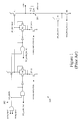
- FIG. 1 is a schematic diagram of an existing memory array output control circuit
- FIG. 2 is a schematic diagram of a memory array output control circuit, in accordance with an embodiment of the invention.
- FIG. 3 is a timing diagram illustrating the operation of the control circuit of FIG. 2 .
- the embodiments herein address the “fast read before write” problem by internally bypassing the SRAM local bitline structure and writing the input data into an existing latch embedded internally in the memory. More specifically, the disclosed embodiments expand on an existing structure in many SRAMs that in turn allows somewhat arbitrary functions of the input data to be presented at the output of the SRAM, with similar timing as data that would normally be read from the SRAM. Since the data is presented at the output with similar timing to that of data that is read from the memory, the disclosed approach does not add to the timing complexities of the downstream logic. The embodiments herein eliminate the need for additional staging latches and downstream multiplexers.
- FIG. 1 there is shown a schematic diagram of an existing memory array output control circuit 100 for an SRAM array.
- gating and multiplexing functions are shown for an upper portion of the SRAM array only, but it will be understood that similar circuitry is also used to perform the same functions for a lower portion of the SRAM array.
- the specific gating devices e.g., AND, NAND, etc.
- FIG. 1 the specific gating devices (e.g., AND, NAND, etc.) shown in the figure are exemplary and could be replaced by other logically equivalent circuits.
- the control circuit includes a timing/gating function, generally depicted at 102 , as well as a multiplexing function depicted by transmission gate pairs TG 0 and TG 1 , which are parallel configured n-type field effect transistor (NFET) and p-type field effect transistor (PFET) devices.
- the multiplexing is used to select between a nominal memory read data path, memory read path (n), and a redundant memory read data path, memory read path (n+m).
- bit lines gbl(n) and a single redundant global bit line gbl(n+m) are shown, although it will be appreciated that several such bit lines (e.g., 16, 32) may be present for each portion of the array.
- the signal gbl_mux_upper representing the multiplexed memory read path output is coupled to a pull up PFET PU, which determines whether the latched output node “output” is charged up from a “reset 0” state. Also, for illustrative purposes, a corresponding pull up PFET PL (controlled by the signal gbl_mux_lower) is shown for the lower portion of the SRAM array. The signal gbl_mux_lower is generated in a similar manner with respect to signal gbl_mux_upper.
- control signals “gating signal” and “timing signal” that are inputs to AND gate 102 are at logic low, or inactive.
- the nominal memory read data path (memory read path (n)) nor the redundant memory read data path, (memory read path (n+m)) affect the output node, which is at a previous state held by a full keeper latch 104 .
- the inputs DC_enable_b(n) and DC_enable_b(n+m) are configured to allow only one of the two transmission gates (TG 0 or TG 1 ) to be on at a given time, in accordance with a memory redundancy scheme.
- the reset_before_evaluate signal will temporarily pulse high, causing the pull down NFET NR and set the full keeper latch 104 and the output signal to a low state.
- both the timing signal (upper or lower) and the gating signal i.e., read enable
- the associated pull up PFET In the case where the selected memory read path contains a logic low value, the associated pull up PFET (PU or PL) remains deactivated, and thus does not disturb the latched “0” state of the output. Conversely, where the selected path contains a logic high value, the associated pull up PFET (PU or PL) is activated, causing the state of the keeper latch 104 and output to change from “0” to “1.”
- the control signals “gating signal” and “timing signal” are such that only one of the pull up PFETs, PU or PL, is active for any given access of the memory array.
- the time when the output changes state is determined by three separate signals, namely reset_before_evaluate, timing signal, and memory read path.
- the reset_before_evaluate signal determines when the output transitions to a preset low state.
- the timing signal has less timing variation than the memory read path signal and is designed to go active sooner than the slowest memory read path and later than the fastest memory read path.
- the port enable signal allows a multiplexed memory read path to be coupled to the output during a write.
- FIG. 2 is a schematic diagram of a memory array output timing control circuit 200 , in accordance with an embodiment of the invention.
- a third port is effectively added to the control circuitry such that the memory read paths are completely decoupled from the output during a write mode. Instead, write data is internally directed to the output node.
- control circuit 200 further provides logic gating, including OR gate 204 and AND gate 206 .
- control circuit 200 of FIG. 2 separates the read enable and write enable control signals.
- the timing signals (from both the upper and lower portions of the SRAM), however, are also used by the bypass circuitry, with the upper and lower timing signals (timing_signal_upper, timing_signal_lower) being input to the OR gate 204 , the output of which is coupled to the AND gate 206 .
- the other input to the AND gate 206 is the separate write_enable control signal.
- PB another pull up PFET
- PB another pull up PFET
- NDT pull down NFET
- NDB pull down NFET
- NET NET
- NEB pull down NFET
- NFET NBE acts as a footer device for the NFET stacks NDT/NET and NDB/NEB, with NBE activated by the output of AND gate 207 , which outputs a port_enable_bypass signal.
- This signal also controls a header PFET PBE to maintain PB in a deactivated state when port_enable_bypass signal is low.
- a half latch 208 (keeper PFET) will also initially maintain the state of the input signal to PB, write_bypass, once port_enable_bypass goes active.
- the write enable signal is held low, which thereby deactivates the port_enable_bypass signal and thus PB is held off. All of the remaining devices of the circuit 200 behave as described above.
- the read_enable_upper signal and corresponding read_enable_lower signal would remain low (inactive), thus preventing memory read paths from activating PU or PL. Instead, the write_enable signal goes high (active).
- the reset_before_evaluate signal still pulses high to set the keeper latch 104 and output node to a low state.
- a logical derivative of the write data into the array is transferred.
- the transferred data would be either the “data in” being written to the top half of the array (data_in_top) or to the bottom half of the array (data_in_bottom), depending on the state of the en_top_data/en_top_data_b control signal pair.
- NFET devices NDT, NDB, NET, and NEB may be replaced by any given pulldown structure and can implement many different functions.
- FIG. 3 is a timing diagram illustrating the various timing relationships of the signals of the control circuit of FIG. 2 .
- the control circuit Prior to time t 1 , the control circuit is in a standby mode, with the state of the output node/keeper latch 104 assumed to be in an unknown previous state.
- a clock signal (clk) goes active low for a memory operation.
- the reset_before_evaluate signal pulses high at time t 2 , so as to activate pull down NFET NR in FIG. 2 , and latch a “0” state at the output/keeper latch at time t 3 .
- the time taken for the reset signal to bring the output/keeper latch to “0” is represented by ⁇ 1 in FIG. 3 .
- Time t 4 represents the earliest case where cell data is available for coupling to the output, pending the activation of the timing signal. Since variation of the arrival of the timing signal is between t 5 and t 6 , it will be seen that the timing signal has less variation than that of the memory read path, where the latest case where cell data is available for coupling to the output is at t 9 (and thus the variation of the memory read path is t 9 -t 4 ).
- this “1” state waits until the arrival of the timing signal before the output/keeper latch can transition from “0” to “1.” If the timing signal also arrives at the earliest point in time at t 5 , then the soonest the output/keeper latch transitions from “0” to “1” is at time t 7 , represented by a delay ⁇ 2 after the rise of the timing signal.
- the output/keeper latch transitions from “0” to “1” at time t 11 , represented by a delay ⁇ 3 after the rise of the memory read path.
- both the earliest and latest rising output edges are determined solely by the timing signal (which again has less variability than the memory read path). That is, the memory read path is effectively taken out of the equation by the bypass circuitry, and as a result the rising output will be within the range as determined by the read case.
- the output/keeper latch transitions from “0” to “1” at time t 8 , represented by a delay ⁇ 4 .
- the output/keeper latch transitions from “0” to “1” at time t 10 , represented by a delay ⁇ 5 .
Abstract
Description
Claims (15)
Priority Applications (1)
| Application Number | Priority Date | Filing Date | Title |
|---|---|---|---|
| US12/822,058 US8345497B2 (en) | 2010-06-23 | 2010-06-23 | Internal bypassing of memory array devices |
Applications Claiming Priority (1)
| Application Number | Priority Date | Filing Date | Title |
|---|---|---|---|
| US12/822,058 US8345497B2 (en) | 2010-06-23 | 2010-06-23 | Internal bypassing of memory array devices |
Publications (2)
| Publication Number | Publication Date |
|---|---|
| US20110317505A1 US20110317505A1 (en) | 2011-12-29 |
| US8345497B2 true US8345497B2 (en) | 2013-01-01 |
Family
ID=45352458
Family Applications (1)
| Application Number | Title | Priority Date | Filing Date |
|---|---|---|---|
| US12/822,058 Expired - Fee Related US8345497B2 (en) | 2010-06-23 | 2010-06-23 | Internal bypassing of memory array devices |
Country Status (1)
| Country | Link |
|---|---|
| US (1) | US8345497B2 (en) |
Cited By (1)
| Publication number | Priority date | Publication date | Assignee | Title |
|---|---|---|---|---|
| CN105765661A (en) * | 2013-11-26 | 2016-07-13 | 高通股份有限公司 | Static random access memory (SRAM) global bitline circuits for reducing power glitches during memory read accesses, and related methods and systems |
Families Citing this family (4)
| Publication number | Priority date | Publication date | Assignee | Title |
|---|---|---|---|---|
| US8345490B2 (en) | 2010-06-23 | 2013-01-01 | International Business Machines Corporation | Split voltage level restore and evaluate clock signals for memory address decoding |
| US8599642B2 (en) | 2010-06-23 | 2013-12-03 | International Business Machines Corporation | Port enable signal generation for gating a memory array device output |
| US8351278B2 (en) | 2010-06-23 | 2013-01-08 | International Business Machines Corporation | Jam latch for latching memory array output data |
| US9588573B2 (en) | 2013-10-28 | 2017-03-07 | Globalfoundries Inc. | Reduced-power trace array for a processor |
Citations (39)
| Publication number | Priority date | Publication date | Assignee | Title |
|---|---|---|---|---|
| US4998221A (en) | 1989-10-31 | 1991-03-05 | International Business Machines Corporation | Memory by-pass for write through read operations |
| US5146427A (en) | 1989-08-30 | 1992-09-08 | Hitachi Ltd. | High speed semiconductor memory having a direct-bypass signal path |
| US5376849A (en) | 1992-12-04 | 1994-12-27 | International Business Machines Corporation | High resolution programmable pulse generator employing controllable delay |
| US5450357A (en) | 1994-04-01 | 1995-09-12 | Texas Instruments Incorporated | Level shifter circuit |
| US5612916A (en) | 1995-12-20 | 1997-03-18 | Intel Corporation | Memory bypass mode |
| US5623217A (en) | 1996-02-26 | 1997-04-22 | Lucent Technologies Inc. | Field programmable gate array with write-port enabled memory |
| US5726677A (en) | 1992-07-07 | 1998-03-10 | Seiko Epson Corporation | Matrix display apparatus, matrix display control apparatus, and matrix display drive apparatus |
| US5818409A (en) | 1994-12-26 | 1998-10-06 | Hitachi, Ltd. | Driving circuits for a passive matrix LCD which uses orthogonal functions to select different groups of scanning electrodes |
| US5952859A (en) | 1998-03-09 | 1999-09-14 | Sun Microsystems, Inc. | Dynamic set/reset circuit with dual feedback |
| US6061296A (en) | 1998-08-17 | 2000-05-09 | Vanguard International Semiconductor Corporation | Multiple data clock activation with programmable delay for use in multiple CAS latency memory devices |
| US6084454A (en) | 1998-08-26 | 2000-07-04 | Advanced Micro Devices, Inc. | Start-up circuit for write selects and equilibrates |
| WO2001056084A1 (en) | 2000-01-26 | 2001-08-02 | Qualcomm Incorporated | Low power dissipation mos jam latch |
| KR100298181B1 (en) | 1997-06-30 | 2001-08-07 | 박종섭 | Register file having a plurality of read/write and bypass path |
| US6356473B1 (en) | 1999-06-24 | 2002-03-12 | Nec Corporation | Static random access memory (SRAM) |
| US6377098B1 (en) | 2000-04-21 | 2002-04-23 | International Business Machines Corporation | CMOS latch having a selectable feedback path |
| US6384754B1 (en) | 1997-06-23 | 2002-05-07 | Samsung Electronics Co., Ltd. | Decoder testing apparatus and methods that simultaneously apply the same multibit input data to multiple decoders |
| US6510089B2 (en) | 1999-12-01 | 2003-01-21 | Kabushiki Kaisha Toshiba | Voltage-level shifter and semiconductor memory using the same |
| US7042262B2 (en) | 2003-10-31 | 2006-05-09 | Sun Microsystems, Inc. | System and method for providing a fast and power efficient jam latch |
| US7075855B1 (en) | 2005-02-08 | 2006-07-11 | International Business Machines Corporation | Memory output timing control circuit with merged functions |
| US20070002619A1 (en) | 2005-06-28 | 2007-01-04 | Tim Schoenauer | Bistable multivibrator with non-volatile state storage |
| US7233542B2 (en) | 2005-02-11 | 2007-06-19 | International Business Machines Corporation | Method and apparatus for address generation |
| US7246279B2 (en) | 2000-06-08 | 2007-07-17 | Sun Microsystems, Inc. | Static random access memory (SRAM) unit and method for operating the same |
| US20080029839A1 (en) | 2006-07-27 | 2008-02-07 | Arm Limited | Controlling signal levels on a signal line within an integrated circuit |
| US7363526B1 (en) | 2004-09-07 | 2008-04-22 | Altera Corporation | Method for transferring data across different clock domains with selectable delay |
| US7425855B2 (en) | 2005-07-14 | 2008-09-16 | International Business Machines Corporation | Set/reset latch with minimum single event upset |
| US20080258790A1 (en) | 2007-04-17 | 2008-10-23 | Texas Instruments Incorporated | Systems and Devices for Sub-threshold Data Capture |
| US7443223B2 (en) | 2006-08-31 | 2008-10-28 | Freescale Semiconductor, Inc. | Level shifting circuit |
| US7463545B2 (en) | 2006-03-17 | 2008-12-09 | Texas Instruments Incorporated | System and method for reducing latency in a memory array decoder circuit |
| US20090059653A1 (en) * | 2007-01-16 | 2009-03-05 | International Business Machines Corporation | Multi-port dynamic memory methods |
| US7515482B2 (en) | 2005-09-29 | 2009-04-07 | Hynix Semiconductor Inc. | Pipe latch device of semiconductor memory device |
| US20090109766A1 (en) | 2007-10-24 | 2009-04-30 | Esin Terzioglu | Efficient sense command generation |
| US7535776B1 (en) | 2008-07-10 | 2009-05-19 | International Business Machines Corporation | Circuit for improved SRAM write around with reduced read access penalty |
| US7596053B1 (en) | 2004-06-14 | 2009-09-29 | Marvell International Ltd. | Integrated memory controller |
| US20100039872A1 (en) | 2008-08-15 | 2010-02-18 | Qualcomm Incorporated | Dual Power Scheme in Memory Circuit |
| US7668037B2 (en) | 2007-11-06 | 2010-02-23 | International Business Machines Corporation | Storage array including a local clock buffer with programmable timing |
| US7710796B2 (en) | 2007-11-06 | 2010-05-04 | International Business Machines Corporation | Level shifter for boosting wordline voltage and memory cell performance |
| US20110320851A1 (en) | 2010-06-23 | 2011-12-29 | International Business Machines Corporation | Port enable signal generation for gating a memory array device output |
| US20110317499A1 (en) | 2010-06-23 | 2011-12-29 | International Business Machines Corporation | Split voltage level restore and evaluate clock signals for memory address decoding |
| US20110317496A1 (en) | 2010-06-23 | 2011-12-29 | International Business Machines Corporation | Jam latch for latching memory array output data |
-
2010
- 2010-06-23 US US12/822,058 patent/US8345497B2/en not_active Expired - Fee Related
Patent Citations (39)
| Publication number | Priority date | Publication date | Assignee | Title |
|---|---|---|---|---|
| US5146427A (en) | 1989-08-30 | 1992-09-08 | Hitachi Ltd. | High speed semiconductor memory having a direct-bypass signal path |
| US4998221A (en) | 1989-10-31 | 1991-03-05 | International Business Machines Corporation | Memory by-pass for write through read operations |
| US5726677A (en) | 1992-07-07 | 1998-03-10 | Seiko Epson Corporation | Matrix display apparatus, matrix display control apparatus, and matrix display drive apparatus |
| US5376849A (en) | 1992-12-04 | 1994-12-27 | International Business Machines Corporation | High resolution programmable pulse generator employing controllable delay |
| US5450357A (en) | 1994-04-01 | 1995-09-12 | Texas Instruments Incorporated | Level shifter circuit |
| US5818409A (en) | 1994-12-26 | 1998-10-06 | Hitachi, Ltd. | Driving circuits for a passive matrix LCD which uses orthogonal functions to select different groups of scanning electrodes |
| US5612916A (en) | 1995-12-20 | 1997-03-18 | Intel Corporation | Memory bypass mode |
| US5623217A (en) | 1996-02-26 | 1997-04-22 | Lucent Technologies Inc. | Field programmable gate array with write-port enabled memory |
| US6384754B1 (en) | 1997-06-23 | 2002-05-07 | Samsung Electronics Co., Ltd. | Decoder testing apparatus and methods that simultaneously apply the same multibit input data to multiple decoders |
| KR100298181B1 (en) | 1997-06-30 | 2001-08-07 | 박종섭 | Register file having a plurality of read/write and bypass path |
| US5952859A (en) | 1998-03-09 | 1999-09-14 | Sun Microsystems, Inc. | Dynamic set/reset circuit with dual feedback |
| US6061296A (en) | 1998-08-17 | 2000-05-09 | Vanguard International Semiconductor Corporation | Multiple data clock activation with programmable delay for use in multiple CAS latency memory devices |
| US6084454A (en) | 1998-08-26 | 2000-07-04 | Advanced Micro Devices, Inc. | Start-up circuit for write selects and equilibrates |
| US6356473B1 (en) | 1999-06-24 | 2002-03-12 | Nec Corporation | Static random access memory (SRAM) |
| US6510089B2 (en) | 1999-12-01 | 2003-01-21 | Kabushiki Kaisha Toshiba | Voltage-level shifter and semiconductor memory using the same |
| WO2001056084A1 (en) | 2000-01-26 | 2001-08-02 | Qualcomm Incorporated | Low power dissipation mos jam latch |
| US6377098B1 (en) | 2000-04-21 | 2002-04-23 | International Business Machines Corporation | CMOS latch having a selectable feedback path |
| US7246279B2 (en) | 2000-06-08 | 2007-07-17 | Sun Microsystems, Inc. | Static random access memory (SRAM) unit and method for operating the same |
| US7042262B2 (en) | 2003-10-31 | 2006-05-09 | Sun Microsystems, Inc. | System and method for providing a fast and power efficient jam latch |
| US7596053B1 (en) | 2004-06-14 | 2009-09-29 | Marvell International Ltd. | Integrated memory controller |
| US7363526B1 (en) | 2004-09-07 | 2008-04-22 | Altera Corporation | Method for transferring data across different clock domains with selectable delay |
| US7075855B1 (en) | 2005-02-08 | 2006-07-11 | International Business Machines Corporation | Memory output timing control circuit with merged functions |
| US7233542B2 (en) | 2005-02-11 | 2007-06-19 | International Business Machines Corporation | Method and apparatus for address generation |
| US20070002619A1 (en) | 2005-06-28 | 2007-01-04 | Tim Schoenauer | Bistable multivibrator with non-volatile state storage |
| US7425855B2 (en) | 2005-07-14 | 2008-09-16 | International Business Machines Corporation | Set/reset latch with minimum single event upset |
| US7515482B2 (en) | 2005-09-29 | 2009-04-07 | Hynix Semiconductor Inc. | Pipe latch device of semiconductor memory device |
| US7463545B2 (en) | 2006-03-17 | 2008-12-09 | Texas Instruments Incorporated | System and method for reducing latency in a memory array decoder circuit |
| US20080029839A1 (en) | 2006-07-27 | 2008-02-07 | Arm Limited | Controlling signal levels on a signal line within an integrated circuit |
| US7443223B2 (en) | 2006-08-31 | 2008-10-28 | Freescale Semiconductor, Inc. | Level shifting circuit |
| US20090059653A1 (en) * | 2007-01-16 | 2009-03-05 | International Business Machines Corporation | Multi-port dynamic memory methods |
| US20080258790A1 (en) | 2007-04-17 | 2008-10-23 | Texas Instruments Incorporated | Systems and Devices for Sub-threshold Data Capture |
| US20090109766A1 (en) | 2007-10-24 | 2009-04-30 | Esin Terzioglu | Efficient sense command generation |
| US7668037B2 (en) | 2007-11-06 | 2010-02-23 | International Business Machines Corporation | Storage array including a local clock buffer with programmable timing |
| US7710796B2 (en) | 2007-11-06 | 2010-05-04 | International Business Machines Corporation | Level shifter for boosting wordline voltage and memory cell performance |
| US7535776B1 (en) | 2008-07-10 | 2009-05-19 | International Business Machines Corporation | Circuit for improved SRAM write around with reduced read access penalty |
| US20100039872A1 (en) | 2008-08-15 | 2010-02-18 | Qualcomm Incorporated | Dual Power Scheme in Memory Circuit |
| US20110320851A1 (en) | 2010-06-23 | 2011-12-29 | International Business Machines Corporation | Port enable signal generation for gating a memory array device output |
| US20110317499A1 (en) | 2010-06-23 | 2011-12-29 | International Business Machines Corporation | Split voltage level restore and evaluate clock signals for memory address decoding |
| US20110317496A1 (en) | 2010-06-23 | 2011-12-29 | International Business Machines Corporation | Jam latch for latching memory array output data |
Non-Patent Citations (7)
| Title |
|---|
| Disclosed Anonymously; "A Clocked Single Supply Level Shifter with Buit-In Firewall;" IP.COM Technical Disclosure; Feb. 3, 2009; pp. 1-5. |
| IBM and Ristard; "Programmable Pulse Generator," IP.COM Technical Disclosure; May 1, 1975; pp. 1-3. |
| IBM TDB Ristard CH; "Programmable Pulse Generator;" IP.COM Technical Disclosure; May 1, 1975. |
| IBM; "Level Shifter Incorporated into Address Pre-decode Circuit for SRAMs Employing 2 Voltage Planes;" IP.COM Technical Disclosure; Jan. 6, 2009; pp. 1-5. |
| J. Davis et al.; "A .6GHZ 64KB Dual-Read Data Cache for the Power6 Processor," IEEE International Solid-State Circuits Conference; 2006. |
| U.S. Appl. No. 12/821,824; Non-Final Office Action; Date Filed: Jun. 23, 2010; Date Mailed: May 11, 2012; pp. 1-9. |
| U.S. Appl. No. 12/822,038; Non-Final Office Action; Date Filed Jun. 23, 2010; Date Mailed: May 15, 2012; pp. 1-11. |
Cited By (2)
| Publication number | Priority date | Publication date | Assignee | Title |
|---|---|---|---|---|
| CN105765661A (en) * | 2013-11-26 | 2016-07-13 | 高通股份有限公司 | Static random access memory (SRAM) global bitline circuits for reducing power glitches during memory read accesses, and related methods and systems |
| CN105765661B (en) * | 2013-11-26 | 2018-08-28 | 高通股份有限公司 | Static RAM (SRAM) global bit line circuit and its correlation technique for reducing the electric power glitch during memory read access and system |
Also Published As
| Publication number | Publication date |
|---|---|
| US20110317505A1 (en) | 2011-12-29 |
Similar Documents
| Publication | Publication Date | Title |
|---|---|---|
| US8351278B2 (en) | Jam latch for latching memory array output data | |
| JP3031840B2 (en) | Precharged sense amplifier | |
| US9478269B2 (en) | Tracking mechanisms | |
| US9064561B2 (en) | Handling of write operations within a memory device | |
| CN110610729A (en) | Apparatus and method for reducing sense amplifier leakage current during active power down | |
| US8767494B2 (en) | Far end resistance tracking design with near end pre-charge control for faster recovery time | |
| US6608785B2 (en) | Method and apparatus to ensure functionality and timing robustness in SOI circuits | |
| US8345497B2 (en) | Internal bypassing of memory array devices | |
| US9570154B2 (en) | Dual-port SRAM timing control circuit which can reduce the operational power consumption of SRAM without affecting the read reliability | |
| US8599642B2 (en) | Port enable signal generation for gating a memory array device output | |
| US8351287B1 (en) | Bitline floating circuit for memory power reduction | |
| US6519197B2 (en) | Sense amplifier with improved read access | |
| US6658544B2 (en) | Techniques to asynchronously operate a synchronous memory | |
| JP4379641B2 (en) | Data readout circuit | |
| US8427899B2 (en) | Self-adaptive sensing design | |
| US9281055B2 (en) | Memory sense amplifier and column pre-charger | |
| US8854902B2 (en) | Write self timing circuitry for self-timed memory | |
| US6996019B2 (en) | Semiconductor device having sense amplifier driver that controls enabling timing | |
| JP3357634B2 (en) | High-speed single-ended sensing with configurable half-latch | |
| US8982609B2 (en) | Memory having read assist device and method of operating the same | |
| US6757852B1 (en) | Self resetting high speed redundancy circuit and method thereof | |
| US5828239A (en) | Sense amplifier circuit with minimized clock skew effect | |
| US9281027B1 (en) | Test techniques in memory devices | |
| JPH10188568A (en) | Reference clock-generating circuit | |
| US8130566B2 (en) | Sense amplifier and method of sensing data using the same |
Legal Events
| Date | Code | Title | Description |
|---|---|---|---|
| AS | Assignment |
Owner name: INTERNATIONAL BUSINESS MACHINES CORPORATION, NEW Y Free format text: ASSIGNMENT OF ASSIGNORS INTEREST;ASSIGNORS:BUNCE, PAUL A.;DAVIS, JOHN D.;HENDERSON, DIANA M.;AND OTHERS;REEL/FRAME:024584/0172 Effective date: 20100623 |
|
| STCF | Information on status: patent grant |
Free format text: PATENTED CASE |
|
| AS | Assignment |
Owner name: GLOBALFOUNDRIES U.S. 2 LLC, NEW YORK Free format text: ASSIGNMENT OF ASSIGNORS INTEREST;ASSIGNOR:INTERNATIONAL BUSINESS MACHINES CORPORATION;REEL/FRAME:036550/0001 Effective date: 20150629 |
|
| AS | Assignment |
Owner name: GLOBALFOUNDRIES INC., CAYMAN ISLANDS Free format text: ASSIGNMENT OF ASSIGNORS INTEREST;ASSIGNORS:GLOBALFOUNDRIES U.S. 2 LLC;GLOBALFOUNDRIES U.S. INC.;REEL/FRAME:036779/0001 Effective date: 20150910 |
|
| FPAY | Fee payment |
Year of fee payment: 4 |
|
| AS | Assignment |
Owner name: WILMINGTON TRUST, NATIONAL ASSOCIATION, DELAWARE Free format text: SECURITY AGREEMENT;ASSIGNOR:GLOBALFOUNDRIES INC.;REEL/FRAME:049490/0001 Effective date: 20181127 |
|
| FEPP | Fee payment procedure |
Free format text: MAINTENANCE FEE REMINDER MAILED (ORIGINAL EVENT CODE: REM.); ENTITY STATUS OF PATENT OWNER: LARGE ENTITY |
|
| AS | Assignment |
Owner name: GLOBALFOUNDRIES INC., CAYMAN ISLANDS Free format text: RELEASE BY SECURED PARTY;ASSIGNOR:WILMINGTON TRUST, NATIONAL ASSOCIATION;REEL/FRAME:054636/0001 Effective date: 20201117 |
|
| LAPS | Lapse for failure to pay maintenance fees |
Free format text: PATENT EXPIRED FOR FAILURE TO PAY MAINTENANCE FEES (ORIGINAL EVENT CODE: EXP.); ENTITY STATUS OF PATENT OWNER: LARGE ENTITY |
|
| STCH | Information on status: patent discontinuation |
Free format text: PATENT EXPIRED DUE TO NONPAYMENT OF MAINTENANCE FEES UNDER 37 CFR 1.362 |
|
| FP | Lapsed due to failure to pay maintenance fee |
Effective date: 20210101 |
|
| AS | Assignment |
Owner name: GLOBALFOUNDRIES U.S. INC., NEW YORK Free format text: RELEASE BY SECURED PARTY;ASSIGNOR:WILMINGTON TRUST, NATIONAL ASSOCIATION;REEL/FRAME:056987/0001 Effective date: 20201117 |