US8350367B2 - Semiconductor device packages with electromagnetic interference shielding - Google Patents
Semiconductor device packages with electromagnetic interference shielding Download PDFInfo
- Publication number
- US8350367B2 US8350367B2 US12/336,400 US33640008A US8350367B2 US 8350367 B2 US8350367 B2 US 8350367B2 US 33640008 A US33640008 A US 33640008A US 8350367 B2 US8350367 B2 US 8350367B2
- Authority
- US
- United States
- Prior art keywords
- substrate unit
- semiconductor device
- grounding
- disposed adjacent
- package
- Prior art date
- Legal status (The legal status is an assumption and is not a legal conclusion. Google has not performed a legal analysis and makes no representation as to the accuracy of the status listed.)
- Active, expires
Links
Images


Classifications
-
- H—ELECTRICITY
- H01—ELECTRIC ELEMENTS
- H01L—SEMICONDUCTOR DEVICES NOT COVERED BY CLASS H10
- H01L21/00—Processes or apparatus adapted for the manufacture or treatment of semiconductor or solid state devices or of parts thereof
- H01L21/67—Apparatus specially adapted for handling semiconductor or electric solid state devices during manufacture or treatment thereof; Apparatus specially adapted for handling wafers during manufacture or treatment of semiconductor or electric solid state devices or components ; Apparatus not specifically provided for elsewhere
- H01L21/683—Apparatus specially adapted for handling semiconductor or electric solid state devices during manufacture or treatment thereof; Apparatus specially adapted for handling wafers during manufacture or treatment of semiconductor or electric solid state devices or components ; Apparatus not specifically provided for elsewhere for supporting or gripping
- H01L21/6835—Apparatus specially adapted for handling semiconductor or electric solid state devices during manufacture or treatment thereof; Apparatus specially adapted for handling wafers during manufacture or treatment of semiconductor or electric solid state devices or components ; Apparatus not specifically provided for elsewhere for supporting or gripping using temporarily an auxiliary support
-
- H—ELECTRICITY
- H01—ELECTRIC ELEMENTS
- H01L—SEMICONDUCTOR DEVICES NOT COVERED BY CLASS H10
- H01L21/00—Processes or apparatus adapted for the manufacture or treatment of semiconductor or solid state devices or of parts thereof
- H01L21/02—Manufacture or treatment of semiconductor devices or of parts thereof
- H01L21/04—Manufacture or treatment of semiconductor devices or of parts thereof the devices having at least one potential-jump barrier or surface barrier, e.g. PN junction, depletion layer or carrier concentration layer
- H01L21/50—Assembly of semiconductor devices using processes or apparatus not provided for in a single one of the subgroups H01L21/06 - H01L21/326, e.g. sealing of a cap to a base of a container
- H01L21/56—Encapsulations, e.g. encapsulation layers, coatings
- H01L21/568—Temporary substrate used as encapsulation process aid
-
- H—ELECTRICITY
- H01—ELECTRIC ELEMENTS
- H01L—SEMICONDUCTOR DEVICES NOT COVERED BY CLASS H10
- H01L23/00—Details of semiconductor or other solid state devices
- H01L23/28—Encapsulations, e.g. encapsulating layers, coatings, e.g. for protection
- H01L23/31—Encapsulations, e.g. encapsulating layers, coatings, e.g. for protection characterised by the arrangement or shape
- H01L23/3107—Encapsulations, e.g. encapsulating layers, coatings, e.g. for protection characterised by the arrangement or shape the device being completely enclosed
- H01L23/3121—Encapsulations, e.g. encapsulating layers, coatings, e.g. for protection characterised by the arrangement or shape the device being completely enclosed a substrate forming part of the encapsulation
-
- H—ELECTRICITY
- H01—ELECTRIC ELEMENTS
- H01L—SEMICONDUCTOR DEVICES NOT COVERED BY CLASS H10
- H01L23/00—Details of semiconductor or other solid state devices
- H01L23/48—Arrangements for conducting electric current to or from the solid state body in operation, e.g. leads, terminal arrangements ; Selection of materials therefor
- H01L23/488—Arrangements for conducting electric current to or from the solid state body in operation, e.g. leads, terminal arrangements ; Selection of materials therefor consisting of soldered or bonded constructions
- H01L23/498—Leads, i.e. metallisations or lead-frames on insulating substrates, e.g. chip carriers
- H01L23/49805—Leads, i.e. metallisations or lead-frames on insulating substrates, e.g. chip carriers the leads being also applied on the sidewalls or the bottom of the substrate, e.g. leadless packages for surface mounting
-
- H—ELECTRICITY
- H01—ELECTRIC ELEMENTS
- H01L—SEMICONDUCTOR DEVICES NOT COVERED BY CLASS H10
- H01L23/00—Details of semiconductor or other solid state devices
- H01L23/552—Protection against radiation, e.g. light or electromagnetic waves
-
- H—ELECTRICITY
- H01—ELECTRIC ELEMENTS
- H01L—SEMICONDUCTOR DEVICES NOT COVERED BY CLASS H10
- H01L24/00—Arrangements for connecting or disconnecting semiconductor or solid-state bodies; Methods or apparatus related thereto
- H01L24/93—Batch processes
- H01L24/95—Batch processes at chip-level, i.e. with connecting carried out on a plurality of singulated devices, i.e. on diced chips
- H01L24/97—Batch processes at chip-level, i.e. with connecting carried out on a plurality of singulated devices, i.e. on diced chips the devices being connected to a common substrate, e.g. interposer, said common substrate being separable into individual assemblies after connecting
-
- H—ELECTRICITY
- H01—ELECTRIC ELEMENTS
- H01L—SEMICONDUCTOR DEVICES NOT COVERED BY CLASS H10
- H01L2221/00—Processes or apparatus adapted for the manufacture or treatment of semiconductor or solid state devices or of parts thereof covered by H01L21/00
- H01L2221/67—Apparatus for handling semiconductor or electric solid state devices during manufacture or treatment thereof; Apparatus for handling wafers during manufacture or treatment of semiconductor or electric solid state devices or components; Apparatus not specifically provided for elsewhere
- H01L2221/683—Apparatus for handling semiconductor or electric solid state devices during manufacture or treatment thereof; Apparatus for handling wafers during manufacture or treatment of semiconductor or electric solid state devices or components; Apparatus not specifically provided for elsewhere for supporting or gripping
- H01L2221/68304—Apparatus for handling semiconductor or electric solid state devices during manufacture or treatment thereof; Apparatus for handling wafers during manufacture or treatment of semiconductor or electric solid state devices or components; Apparatus not specifically provided for elsewhere for supporting or gripping using temporarily an auxiliary support
- H01L2221/68345—Apparatus for handling semiconductor or electric solid state devices during manufacture or treatment thereof; Apparatus for handling wafers during manufacture or treatment of semiconductor or electric solid state devices or components; Apparatus not specifically provided for elsewhere for supporting or gripping using temporarily an auxiliary support used as a support during the manufacture of self supporting substrates
-
- H—ELECTRICITY
- H01—ELECTRIC ELEMENTS
- H01L—SEMICONDUCTOR DEVICES NOT COVERED BY CLASS H10
- H01L2224/00—Indexing scheme for arrangements for connecting or disconnecting semiconductor or solid-state bodies and methods related thereto as covered by H01L24/00
- H01L2224/01—Means for bonding being attached to, or being formed on, the surface to be connected, e.g. chip-to-package, die-attach, "first-level" interconnects; Manufacturing methods related thereto
- H01L2224/10—Bump connectors; Manufacturing methods related thereto
- H01L2224/15—Structure, shape, material or disposition of the bump connectors after the connecting process
- H01L2224/16—Structure, shape, material or disposition of the bump connectors after the connecting process of an individual bump connector
- H01L2224/161—Disposition
- H01L2224/16151—Disposition the bump connector connecting between a semiconductor or solid-state body and an item not being a semiconductor or solid-state body, e.g. chip-to-substrate, chip-to-passive
- H01L2224/16221—Disposition the bump connector connecting between a semiconductor or solid-state body and an item not being a semiconductor or solid-state body, e.g. chip-to-substrate, chip-to-passive the body and the item being stacked
- H01L2224/16225—Disposition the bump connector connecting between a semiconductor or solid-state body and an item not being a semiconductor or solid-state body, e.g. chip-to-substrate, chip-to-passive the body and the item being stacked the item being non-metallic, e.g. insulating substrate with or without metallisation
-
- H—ELECTRICITY
- H01—ELECTRIC ELEMENTS
- H01L—SEMICONDUCTOR DEVICES NOT COVERED BY CLASS H10
- H01L2224/00—Indexing scheme for arrangements for connecting or disconnecting semiconductor or solid-state bodies and methods related thereto as covered by H01L24/00
- H01L2224/01—Means for bonding being attached to, or being formed on, the surface to be connected, e.g. chip-to-package, die-attach, "first-level" interconnects; Manufacturing methods related thereto
- H01L2224/42—Wire connectors; Manufacturing methods related thereto
- H01L2224/47—Structure, shape, material or disposition of the wire connectors after the connecting process
- H01L2224/48—Structure, shape, material or disposition of the wire connectors after the connecting process of an individual wire connector
- H01L2224/4805—Shape
- H01L2224/4809—Loop shape
- H01L2224/48091—Arched
-
- H—ELECTRICITY
- H01—ELECTRIC ELEMENTS
- H01L—SEMICONDUCTOR DEVICES NOT COVERED BY CLASS H10
- H01L2224/00—Indexing scheme for arrangements for connecting or disconnecting semiconductor or solid-state bodies and methods related thereto as covered by H01L24/00
- H01L2224/01—Means for bonding being attached to, or being formed on, the surface to be connected, e.g. chip-to-package, die-attach, "first-level" interconnects; Manufacturing methods related thereto
- H01L2224/42—Wire connectors; Manufacturing methods related thereto
- H01L2224/47—Structure, shape, material or disposition of the wire connectors after the connecting process
- H01L2224/48—Structure, shape, material or disposition of the wire connectors after the connecting process of an individual wire connector
- H01L2224/481—Disposition
- H01L2224/48151—Connecting between a semiconductor or solid-state body and an item not being a semiconductor or solid-state body, e.g. chip-to-substrate, chip-to-passive
- H01L2224/48221—Connecting between a semiconductor or solid-state body and an item not being a semiconductor or solid-state body, e.g. chip-to-substrate, chip-to-passive the body and the item being stacked
- H01L2224/48225—Connecting between a semiconductor or solid-state body and an item not being a semiconductor or solid-state body, e.g. chip-to-substrate, chip-to-passive the body and the item being stacked the item being non-metallic, e.g. insulating substrate with or without metallisation
- H01L2224/48227—Connecting between a semiconductor or solid-state body and an item not being a semiconductor or solid-state body, e.g. chip-to-substrate, chip-to-passive the body and the item being stacked the item being non-metallic, e.g. insulating substrate with or without metallisation connecting the wire to a bond pad of the item
-
- H—ELECTRICITY
- H01—ELECTRIC ELEMENTS
- H01L—SEMICONDUCTOR DEVICES NOT COVERED BY CLASS H10
- H01L2224/00—Indexing scheme for arrangements for connecting or disconnecting semiconductor or solid-state bodies and methods related thereto as covered by H01L24/00
- H01L2224/01—Means for bonding being attached to, or being formed on, the surface to be connected, e.g. chip-to-package, die-attach, "first-level" interconnects; Manufacturing methods related thereto
- H01L2224/42—Wire connectors; Manufacturing methods related thereto
- H01L2224/47—Structure, shape, material or disposition of the wire connectors after the connecting process
- H01L2224/49—Structure, shape, material or disposition of the wire connectors after the connecting process of a plurality of wire connectors
- H01L2224/491—Disposition
- H01L2224/4912—Layout
- H01L2224/49175—Parallel arrangements
-
- H—ELECTRICITY
- H01—ELECTRIC ELEMENTS
- H01L—SEMICONDUCTOR DEVICES NOT COVERED BY CLASS H10
- H01L2224/00—Indexing scheme for arrangements for connecting or disconnecting semiconductor or solid-state bodies and methods related thereto as covered by H01L24/00
- H01L2224/93—Batch processes
- H01L2224/95—Batch processes at chip-level, i.e. with connecting carried out on a plurality of singulated devices, i.e. on diced chips
- H01L2224/97—Batch processes at chip-level, i.e. with connecting carried out on a plurality of singulated devices, i.e. on diced chips the devices being connected to a common substrate, e.g. interposer, said common substrate being separable into individual assemblies after connecting
-
- H—ELECTRICITY
- H01—ELECTRIC ELEMENTS
- H01L—SEMICONDUCTOR DEVICES NOT COVERED BY CLASS H10
- H01L24/00—Arrangements for connecting or disconnecting semiconductor or solid-state bodies; Methods or apparatus related thereto
- H01L24/01—Means for bonding being attached to, or being formed on, the surface to be connected, e.g. chip-to-package, die-attach, "first-level" interconnects; Manufacturing methods related thereto
- H01L24/42—Wire connectors; Manufacturing methods related thereto
- H01L24/47—Structure, shape, material or disposition of the wire connectors after the connecting process
- H01L24/48—Structure, shape, material or disposition of the wire connectors after the connecting process of an individual wire connector
-
- H—ELECTRICITY
- H01—ELECTRIC ELEMENTS
- H01L—SEMICONDUCTOR DEVICES NOT COVERED BY CLASS H10
- H01L24/00—Arrangements for connecting or disconnecting semiconductor or solid-state bodies; Methods or apparatus related thereto
- H01L24/01—Means for bonding being attached to, or being formed on, the surface to be connected, e.g. chip-to-package, die-attach, "first-level" interconnects; Manufacturing methods related thereto
- H01L24/42—Wire connectors; Manufacturing methods related thereto
- H01L24/47—Structure, shape, material or disposition of the wire connectors after the connecting process
- H01L24/49—Structure, shape, material or disposition of the wire connectors after the connecting process of a plurality of wire connectors
-
- H—ELECTRICITY
- H01—ELECTRIC ELEMENTS
- H01L—SEMICONDUCTOR DEVICES NOT COVERED BY CLASS H10
- H01L2924/00—Indexing scheme for arrangements or methods for connecting or disconnecting semiconductor or solid-state bodies as covered by H01L24/00
- H01L2924/0001—Technical content checked by a classifier
- H01L2924/00014—Technical content checked by a classifier the subject-matter covered by the group, the symbol of which is combined with the symbol of this group, being disclosed without further technical details
-
- H—ELECTRICITY
- H01—ELECTRIC ELEMENTS
- H01L—SEMICONDUCTOR DEVICES NOT COVERED BY CLASS H10
- H01L2924/00—Indexing scheme for arrangements or methods for connecting or disconnecting semiconductor or solid-state bodies as covered by H01L24/00
- H01L2924/01—Chemical elements
- H01L2924/01005—Boron [B]
-
- H—ELECTRICITY
- H01—ELECTRIC ELEMENTS
- H01L—SEMICONDUCTOR DEVICES NOT COVERED BY CLASS H10
- H01L2924/00—Indexing scheme for arrangements or methods for connecting or disconnecting semiconductor or solid-state bodies as covered by H01L24/00
- H01L2924/01—Chemical elements
- H01L2924/01006—Carbon [C]
-
- H—ELECTRICITY
- H01—ELECTRIC ELEMENTS
- H01L—SEMICONDUCTOR DEVICES NOT COVERED BY CLASS H10
- H01L2924/00—Indexing scheme for arrangements or methods for connecting or disconnecting semiconductor or solid-state bodies as covered by H01L24/00
- H01L2924/01—Chemical elements
- H01L2924/01013—Aluminum [Al]
-
- H—ELECTRICITY
- H01—ELECTRIC ELEMENTS
- H01L—SEMICONDUCTOR DEVICES NOT COVERED BY CLASS H10
- H01L2924/00—Indexing scheme for arrangements or methods for connecting or disconnecting semiconductor or solid-state bodies as covered by H01L24/00
- H01L2924/01—Chemical elements
- H01L2924/01024—Chromium [Cr]
-
- H—ELECTRICITY
- H01—ELECTRIC ELEMENTS
- H01L—SEMICONDUCTOR DEVICES NOT COVERED BY CLASS H10
- H01L2924/00—Indexing scheme for arrangements or methods for connecting or disconnecting semiconductor or solid-state bodies as covered by H01L24/00
- H01L2924/01—Chemical elements
- H01L2924/01027—Cobalt [Co]
-
- H—ELECTRICITY
- H01—ELECTRIC ELEMENTS
- H01L—SEMICONDUCTOR DEVICES NOT COVERED BY CLASS H10
- H01L2924/00—Indexing scheme for arrangements or methods for connecting or disconnecting semiconductor or solid-state bodies as covered by H01L24/00
- H01L2924/01—Chemical elements
- H01L2924/01029—Copper [Cu]
-
- H—ELECTRICITY
- H01—ELECTRIC ELEMENTS
- H01L—SEMICONDUCTOR DEVICES NOT COVERED BY CLASS H10
- H01L2924/00—Indexing scheme for arrangements or methods for connecting or disconnecting semiconductor or solid-state bodies as covered by H01L24/00
- H01L2924/01—Chemical elements
- H01L2924/01033—Arsenic [As]
-
- H—ELECTRICITY
- H01—ELECTRIC ELEMENTS
- H01L—SEMICONDUCTOR DEVICES NOT COVERED BY CLASS H10
- H01L2924/00—Indexing scheme for arrangements or methods for connecting or disconnecting semiconductor or solid-state bodies as covered by H01L24/00
- H01L2924/01—Chemical elements
- H01L2924/01047—Silver [Ag]
-
- H—ELECTRICITY
- H01—ELECTRIC ELEMENTS
- H01L—SEMICONDUCTOR DEVICES NOT COVERED BY CLASS H10
- H01L2924/00—Indexing scheme for arrangements or methods for connecting or disconnecting semiconductor or solid-state bodies as covered by H01L24/00
- H01L2924/01—Chemical elements
- H01L2924/01075—Rhenium [Re]
-
- H—ELECTRICITY
- H01—ELECTRIC ELEMENTS
- H01L—SEMICONDUCTOR DEVICES NOT COVERED BY CLASS H10
- H01L2924/00—Indexing scheme for arrangements or methods for connecting or disconnecting semiconductor or solid-state bodies as covered by H01L24/00
- H01L2924/01—Chemical elements
- H01L2924/01078—Platinum [Pt]
-
- H—ELECTRICITY
- H01—ELECTRIC ELEMENTS
- H01L—SEMICONDUCTOR DEVICES NOT COVERED BY CLASS H10
- H01L2924/00—Indexing scheme for arrangements or methods for connecting or disconnecting semiconductor or solid-state bodies as covered by H01L24/00
- H01L2924/01—Chemical elements
- H01L2924/01079—Gold [Au]
-
- H—ELECTRICITY
- H01—ELECTRIC ELEMENTS
- H01L—SEMICONDUCTOR DEVICES NOT COVERED BY CLASS H10
- H01L2924/00—Indexing scheme for arrangements or methods for connecting or disconnecting semiconductor or solid-state bodies as covered by H01L24/00
- H01L2924/01—Chemical elements
- H01L2924/01082—Lead [Pb]
-
- H—ELECTRICITY
- H01—ELECTRIC ELEMENTS
- H01L—SEMICONDUCTOR DEVICES NOT COVERED BY CLASS H10
- H01L2924/00—Indexing scheme for arrangements or methods for connecting or disconnecting semiconductor or solid-state bodies as covered by H01L24/00
- H01L2924/15—Details of package parts other than the semiconductor or other solid state devices to be connected
- H01L2924/151—Die mounting substrate
- H01L2924/153—Connection portion
- H01L2924/1531—Connection portion the connection portion being formed only on the surface of the substrate opposite to the die mounting surface
- H01L2924/15311—Connection portion the connection portion being formed only on the surface of the substrate opposite to the die mounting surface being a ball array, e.g. BGA
-
- H—ELECTRICITY
- H01—ELECTRIC ELEMENTS
- H01L—SEMICONDUCTOR DEVICES NOT COVERED BY CLASS H10
- H01L2924/00—Indexing scheme for arrangements or methods for connecting or disconnecting semiconductor or solid-state bodies as covered by H01L24/00
- H01L2924/15—Details of package parts other than the semiconductor or other solid state devices to be connected
- H01L2924/181—Encapsulation
-
- H—ELECTRICITY
- H01—ELECTRIC ELEMENTS
- H01L—SEMICONDUCTOR DEVICES NOT COVERED BY CLASS H10
- H01L2924/00—Indexing scheme for arrangements or methods for connecting or disconnecting semiconductor or solid-state bodies as covered by H01L24/00
- H01L2924/19—Details of hybrid assemblies other than the semiconductor or other solid state devices to be connected
- H01L2924/1901—Structure
- H01L2924/1904—Component type
- H01L2924/19041—Component type being a capacitor
-
- H—ELECTRICITY
- H01—ELECTRIC ELEMENTS
- H01L—SEMICONDUCTOR DEVICES NOT COVERED BY CLASS H10
- H01L2924/00—Indexing scheme for arrangements or methods for connecting or disconnecting semiconductor or solid-state bodies as covered by H01L24/00
- H01L2924/19—Details of hybrid assemblies other than the semiconductor or other solid state devices to be connected
- H01L2924/1901—Structure
- H01L2924/1904—Component type
- H01L2924/19042—Component type being an inductor
-
- H—ELECTRICITY
- H01—ELECTRIC ELEMENTS
- H01L—SEMICONDUCTOR DEVICES NOT COVERED BY CLASS H10
- H01L2924/00—Indexing scheme for arrangements or methods for connecting or disconnecting semiconductor or solid-state bodies as covered by H01L24/00
- H01L2924/19—Details of hybrid assemblies other than the semiconductor or other solid state devices to be connected
- H01L2924/1901—Structure
- H01L2924/1904—Component type
- H01L2924/19043—Component type being a resistor
-
- H—ELECTRICITY
- H01—ELECTRIC ELEMENTS
- H01L—SEMICONDUCTOR DEVICES NOT COVERED BY CLASS H10
- H01L2924/00—Indexing scheme for arrangements or methods for connecting or disconnecting semiconductor or solid-state bodies as covered by H01L24/00
- H01L2924/19—Details of hybrid assemblies other than the semiconductor or other solid state devices to be connected
- H01L2924/191—Disposition
- H01L2924/19101—Disposition of discrete passive components
- H01L2924/19105—Disposition of discrete passive components in a side-by-side arrangement on a common die mounting substrate
-
- H—ELECTRICITY
- H01—ELECTRIC ELEMENTS
- H01L—SEMICONDUCTOR DEVICES NOT COVERED BY CLASS H10
- H01L2924/00—Indexing scheme for arrangements or methods for connecting or disconnecting semiconductor or solid-state bodies as covered by H01L24/00
- H01L2924/30—Technical effects
- H01L2924/301—Electrical effects
- H01L2924/3025—Electromagnetic shielding
Definitions
- the invention relates generally to semiconductor device packages. More particularly, the invention relates to semiconductor device packages with electromagnetic interference shielding.
- Electromagnetic emissions can radiate from a source semiconductor device, and can be incident upon neighboring semiconductor devices. If the level of electromagnetic emissions at a neighboring semiconductor device is sufficiently high, these emissions can adversely affect the operation of that semiconductor device. This phenomenon is sometimes referred to as electromagnetic interference (“EMI”). Smaller sizes of semiconductor devices can exacerbate EMI by providing a higher density of those semiconductor devices within an overall electronic system, and, thus, a higher level of undesired electromagnetic emissions at a neighboring semiconductor device.
- EMI electromagnetic interference
- shielding can be accomplished by including an electrically conductive casing or housing that is electrically grounded and is secured to an exterior of the package.
- an electrically conductive casing or housing that is electrically grounded and is secured to an exterior of the package.
- electromagnetic emissions from an interior of the package strike an inner surface of the casing, at least a portion of these emissions can be electrically shorted, thereby reducing the level of emissions that can pass through the casing and adversely affect neighboring semiconductor devices.
- electromagnetic emissions from a neighboring semiconductor device strike an outer surface of the casing, a similar electrical shorting can occur to reduce EMI of semiconductor devices within the package.
- an electrically conductive casing can reduce EMI
- the use of the casing can suffer from a number of disadvantages.
- the casino is typically secured to an exterior of a semiconductor device package by an adhesive.
- the casing can be prone to peeling or falling off, since binding characteristics of the adhesive can be adversely affected by temperature, humidity, and other environmental conditions.
- the size and shape of the casing and the size and shape of the package should match within relatively small tolerance levels. This matching of sizes and shapes and associated precision in relative positioning of the casing and the package can render manufacturing operations costly and time consuming. Because of this matching of sizes and shapes, it also follows that semiconductor device packages of different sizes and shapes can require different casings, which can further increase manufacturing cost and time to accommodate the different packages.
- a semiconductor device package includes: (1) a substrate unit including (a) an upper surface, (b) a lower surface, (c) a lateral surface disposed adjacent to a periphery of the substrate unit, and (d) a grounding element disposed adjacent to the periphery of the substrate unit; (2) a semiconductor device disposed adjacent to the upper surface of the substrate unit and electrically connected to the substrate unit; (3) a package body disposed adjacent to the upper surface of the substrate unit and covering the semiconductor device; and (4) an EMI shield disposed adjacent to exterior surfaces of the package body and electrically connected to a connection surface of the grounding element.
- a lateral surface of the package body is substantially aligned with the lateral surface of the substrate unit, and the connection surface of the grounding element is electrically exposed adjacent to the lateral surface of the substrate unit.
- the grounding element corresponds to a remnant of a grounding via, and provides an electrical pathway to ground electromagnetic emissions incident upon the EMI shield.
- the semiconductor device package includes: (1) a substrate unit including (a) a first surface, (b) a second opposing surface, and (c) a grounding element at least partially extending between the first surface and the second opposing surface; (2) a semiconductor device disposed adjacent to the first surface of the substrate unit and electrically connected to the substrate unit; (3) a package body disposed adjacent to the first surface of the substrate unit and covering the semiconductor device and the grounding element; and (4) an EMI shield disposed adjacent to exterior surfaces of the package body and electrically connected to a lateral surface of the grounding element.
- the lateral surface of the grounding element is disposed adjacent to a periphery of the substrate unit, such that the lateral surface of the grounding element is electrically exposed.
- the grounding element provides an electrical pathway to ground electromagnetic emissions incident upon the EMI shield, and a lateral profile of the semiconductor device package is substantially planar and is substantially orthogonal with respect to the second opposing surface of the substrate unit.
- a method includes: (1) providing a substrate including (a) an upper surface, (b) a lower surface, and (c) grounding vias at least partially extending between the upper surface and the lower surface; (2) electrically connecting a semiconductor device to the upper surface of the substrate; (3) applying a molding material to the upper surface of the substrate to form a molded structure covering the grounding vias and the semiconductor device; (4) forming cutting slits extending through the molded structure and the substrate, and the cutting slits are aligned with the substrate, such that: (a) the substrate is sub-divided to form a substrate unit; (b) the molded structure is sub-divided to form a package body disposed adjacent to the substrate unit; and (c) remnants of the grounding vias correspond to grounding elements disposed adjacent to a periphery of the substrate unit; and (5) applying an EMI coating to exterior surfaces of the package body and exposed connection surfaces of
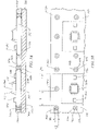
- FIG. 1 illustrates a perspective view of a semiconductor device package implemented in accordance with an embodiment of the invention.
- FIG. 2 illustrates a cross-sectional view of the semiconductor device package of FIG. 1 , taken along line A-A of FIG. 1 .
- FIG. 3 illustrates an enlarged, cross-sectional view of a portion of the semiconductor device package of FIG. 1 .
- FIG. 4 illustrates a cross-sectional view of a semiconductor device package implemented in accordance with another embodiment of the invention.
- FIG. 5A through FIG. 5E illustrate a method of forming the semiconductor device package of FIG. 1 according to an embodiment of the invention.
- FIG. 6 illustrates a method of forming the semiconductor device package of FIG. 4 , according to another embodiment of the invention.
- a set refers to a collection of one or more components.
- a set of layers can include a single layer or multiple layers.
- Components of a set also can be referred to as members of the set.
- Components of a set can be the same or different.
- components of a set can share one or more common characteristics.
- adjacent refers to being near or adjoining. Adjacent components can be spaced apart from one another or can be in actual or direct contact with one another. In some instances, adjacent components can be connected to one another or can be formed integrally with one another.
- the terms “inner,” “outer,” “upper,” “upwardly,” “lower,” “downwardly,” “lateral,” and “laterally” refer to a relative orientation of a set of components, such as in accordance with the drawings, but do not require a particular orientation of those components during manufacturing or use.
- connection refers to an operational coupling or linking.
- Connected components can be directly coupled to one another or can be indirectly coupled to one another, such as via another set of components.
- the terms “substantially” and “substantial” refer to a considerable degree or extent. When used in conjunction with an event or circumstance, the terms can refer to instances in which the event or circumstance occurs precisely as well as instances in which the event or circumstance occurs to a close approximation, such as accounting for typical tolerance levels of the manufacturing operations described herein.
- electrically conductive and “electrical conductivity” refer to an ability to transport an electric current. Electrically conductive materials typically correspond to those materials that exhibit little or no opposition to flow of an electric current. One measure of electrical conductivity is in terms of Siemens per meter (“S ⁇ m ⁇ 1 ”). Typically, an electrically conductive material is one having a conductivity greater than about 10 4 S ⁇ m ⁇ 1 , such as at least about 10 5 S ⁇ m ⁇ 1 or at least about 10 6 S ⁇ m ⁇ 1 . Electrical conductivity of a material can sometimes vary with temperature. Unless otherwise specified, electrical conductivity of a material is defined at room temperature.
- FIG. 1 and FIG. 2 illustrate a semiconductor device package 100 implemented in accordance with an embodiment of the invention.
- FIG. 1 illustrates a perspective view of the package 100
- FIG. 2 illustrates a cross-sectional view of the package 100 , taken along line A-A of FIG. 1 .
- sides of the package 100 are substantially planar and have a substantially orthogonal orientation so as to define a lateral profile that extends around substantially an entire periphery of the package 100 .
- this orthogonal lateral profile allows a reduced overall package size by reducing or minimizing a footprint area of the package 100 .
- the lateral profile of the package 100 in general, can be any of a number of shapes, such as curved, inclined, stepped, or roughly textured.
- the package 100 includes a substrate unit 102 , which includes an upper surface 104 , a lower surface 106 , and lateral surfaces 142 and 144 disposed adjacent to sides of the substrate unit 102 .
- the lateral surfaces 142 and 144 are substantially planar and have a substantially orthogonal orientation with respect to the upper surface 104 or the lower surface 106 , although it is contemplated that the shapes and orientations of the lateral surfaces 142 and 144 can vary for other implementations.
- the substrate unit 102 can be implemented in a number of ways, and includes electrical interconnect to provide electrical pathways between the upper surface 104 and the lower surface 106 of the substrate unit 102 .
- the electrical interconnect can include, for example, a set of electrically conductive layers that are incorporated within a set of dielectric layers.
- the electrically conductive layers can be connected to one another by internal vias, and can be implemented so as to sandwich a core formed from a suitable resin, such as one based on bismaleimide and triazine or based on epoxy and polyphenylene oxide.
- the substrate unit 102 can include a substantially slab-shaped core that is sandwiched by one set of electrically conductive layers disposed adjacent to an upper surface of the core and another set of electrically conductive layers disposed adjacent to a lower surface of the core.
- a thickness of the substrate unit 102 namely a distance between the upper surface 104 and the lower surface 106 of the substrate unit 102 , can be in the range of about 0.1 millimeter (“mm”) to about 2 mm, such as from about 0.2 mm to about 1.5 mm or from about 0.4 mm to about 0.6 mm. While not illustrated in FIG. 2 , it is contemplated that a solder mask layer can be disposed adjacent to either, or both, the upper surface 104 and the lower surface 106 of the substrate unit 102 .
- the substrate unit 102 includes grounding elements 118 a and 118 b , which are disposed adjacent to a periphery of the substrate unit 102 . More particularly, the grounding elements 118 a and 118 b are disposed substantially at the periphery of the substrate unit 102 , and are disposed adjacent to the lateral surfaces 142 and 144 , respectively. The grounding elements 118 a and 118 b are connected to other electrical interconnect included in the substrate unit 102 and, as further described below, provide electrical pathways to reduce EMI.
- each of the grounding elements 118 a and 118 b is implemented as grounding vias and, more particularly, as remnants of grounding vias in accordance with a set of singulation operations as further described below.
- each of the grounding elements 118 a and 118 b includes an upper via pad remnant 146 a or 146 b , which is disposed adjacent to the upper surface 104 of the substrate unit 102 , a lower via pad remnant 148 a or 148 b , which is disposed adjacent to the lower surface 106 of the substrate unit 102 , and a plated channel remnant 150 a or 150 b , which extends between the upper via pad remnant 146 a or 146 b and the lower via pad remnant 148 a or 148 b .
- grounding elements 118 a and 118 b are illustrated as fully extending between the upper surface 104 and the lower surface 106 of the substrate unit 102 , it is contemplated that the extent of the grounding elements 118 a and 118 b can vary for other implementations.
- the grounding elements 118 a and 118 b include connection surfaces S 1 and S 2 , respectively, which are lateral surfaces that face away from an interior of the package 100 and are disposed adjacent to the periphery of the substrate unit 102 . More particularly, the connection surfaces S 1 and S 2 are electrically exposed substantially at the periphery of the substrate unit 102 , and are electrically exposed adjacent to the lateral surfaces 142 and 144 , respectively. In the illustrated embodiment, the connection surfaces S 1 and S 2 correspond to electrically exposed surfaces of the upper via pad remnants 146 a and 146 b , the lower via pad remnants 148 a and 148 b , and the plated channel remnants 150 a and 150 b .
- connection surfaces S 1 and S 2 can enhance reliability and efficiency of electrical connections for reducing EMI.
- the grounding elements 118 a and 118 b are formed from a metal, a metal alloy, a matrix with a metal or a metal alloy dispersed therein, or another suitable electrically conductive material.
- a height H 1 of the grounding elements 118 a and 118 b can be substantially the same as the thickness of the substrate unit 102 , and can be in the range of about 0.1 mm to about 2 mm, such as from about 0.2 mm to about 1.5 mm or from about 0.4 mm to about 0.6 mm.
- a width W 1 of the grounding elements 118 a and 118 b can be in the range of about 75 micrometer (“ ⁇ m”) to about 275 ⁇ m, such as from about 100 ⁇ m to about 250 ⁇ m or from about 125 ⁇ m to about 225 ⁇ m.
- the package 100 also includes semiconductor devices 108 a , 108 b , and 108 c , which are disposed adjacent to the upper surface 104 of the substrate unit 102 , and electrical contacts 110 a , 110 b , and 110 c , which are disposed adjacent to the lower surface 106 of the substrate unit 102 .
- the semiconductor device 108 b is wire-bonded to the substrate unit 102 via a set of wires 112 , which are formed from gold or another suitable electrically conductive material, and the semiconductor devices 108 a and 108 c are surface mounted to the substrate unit 102 .
- the semiconductor device 108 b is a semiconductor chip, while the semiconductor devices 108 a and 108 c are passive devices, such as resistors, capacitors, or inductors.
- the electrical contacts 110 a , 110 b , and 110 c provide input and output electrical connections for the package 100 , and at least a subset of the electrical contacts 110 a , 110 b and 110 c are electrically connected to the semiconductor devices 108 a , 108 b , and 108 c via electrical interconnect included in the substrate unit 102 .
- At least one of the electrical contacts 110 a , 110 b , and 110 c is a ground electrical contact, and is electrically connected to the grounding elements 118 a and 118 b via electrical interconnect included in the substrate unit 102 . While three semiconductor devices are illustrated in FIG. 2 , it is contemplated that more or less semiconductor devices can be included for other implementations, and that semiconductor devices, in general, can be any active devices, any passive devices, or combinations thereof. It is also contemplated that the number of electrical contacts can vary from that illustrated in FIG. 2 .
- the package 100 also includes a package body 114 that is disposed adjacent to the upper surface 104 of the substrate unit 102 .
- the package body 114 substantially covers or encapsulates the grounding elements 118 a and 118 b , the semiconductor devices 108 a , 108 b , and 108 c , and the wires 112 to provide mechanical stability as well as protection against oxidation, humidity, and other environmental conditions.
- the package body 114 is formed from a molding material, and includes exterior surfaces, including lateral surfaces 120 and 122 disposed adjacent to sides of the package body 114 .
- the lateral surfaces 120 and 122 are substantially planar and have a substantially orthogonal orientation with respect to the upper surface 104 or the lower surface 106 , although it is contemplated that the lateral surfaces 120 and 122 can be curved, inclined, or roughly textured for other implementations. Also, the lateral surfaces 120 and 122 are substantially aligned or co-planar with the lateral surfaces 142 and 144 , respectively. More particularly, this alignment is accomplished while allowing the connection surfaces S 1 and S 2 to be electrically exposed, such as by reducing or minimizing coverage of the connection surfaces S 1 and S 2 by the package body 114 .
- the shape of the lateral surfaces 120 and 122 and their alignment with the lateral surfaces 142 and 144 can be varied from that illustrated in FIG. 2 , while allowing the connection surfaces S 1 and S 2 to be at least partially electrically exposed.
- the package 100 further includes an EMI shield 124 that is disposed adjacent to the exterior surfaces of the package body 114 , the connection surfaces S 1 and S 2 of the grounding elements 118 a and 118 b , and the lateral surfaces 142 and 144 of the substrate unit 102 .
- the EMI shield 124 is formed from an electrically conductive material, and substantially surrounds the semiconductor devices 108 a , 108 b , and 108 c within the package 100 to provide protection against EMI.
- the EMI shield 124 includes an upper portion 126 and a lateral portion 128 , which extends around substantially the entire periphery of the package body 114 and defines the orthogonal lateral profile of the package 100 .
- the lateral portion 128 extends downwardly from the upper portion 126 and along the lateral surfaces 142 and 144 of the substrate unit 102 , and includes a lower end that is substantially aligned or co-planar with the lower surface 106 of the substrate unit 102 .
- the extent of the lateral portion 128 and the alignment of its lower end with the lower surface 106 can be varied for other implementations.
- the EMI shield 124 is electrically connected to the connection surfaces S 1 and S 2 of the grounding elements 118 a and 118 b .
- the EMI shield 124 When electromagnetic emissions radiated from an interior of the package 100 strike the EMI shield 124 , at least a portion of these emissions can be efficiently grounded via the grounding elements 118 a and 118 b , thereby reducing the level of emissions that can pass through the EMI shield 124 and adversely affect neighboring semiconductor devices.
- a similar grounding can occur to reduce EMI of the semiconductor devices 108 a , 108 b and 108 c within the package 100 .
- the package 100 can be disposed on a printed circuit board (“PCB”) and electrically connected to the PCB via the electrical contacts 110 a , 110 b , and 110 c .
- PCB printed circuit board
- at least one of the electrical contacts 110 a , 110 b , and 110 c is a ground electrical contact, and the ground electrical contact can be electrically connected to a ground voltage provided by the PCB.
- Grounding of electromagnetic emissions incident upon the EMI shield 124 can occur through an electrical pathway including the grounding elements 118 a and 118 b , other electrical interconnect included in the substrate unit 102 , and the ground electrical contact.
- the lower end of the EMI shield 124 is substantially aligned with the lower surface 106 of the substrate unit 102 , the lower end also can be electrically connected to a ground voltage provided by the PCB, thereby providing an alternative electrical pathway for grounding undesired electromagnetic emissions.
- the lower via pad remnants 148 a and 148 b can be electrically connected to a ground voltage provided by the PCB.
- the EMI shield 124 is a conformal shield that is formed as a set of layers or films.
- the EMI shield 124 can be formed adjacent to and in direct contact with all exterior of the package 100 without the use of an adhesive, thereby enhancing reliability and resistance to temperature, humidity, and other environmental conditions.
- the conformal characteristics of the EMI shield 124 allow similar EMI shields and similar manufacturing operations to be readily applied to semiconductor device packages of different sizes and shapes, thereby reducing manufacturing cost and time to accommodate the different packages.
- a thickness of the EMI shield 124 can be in the range of about 1 ⁇ m to about 500 ⁇ m, such as from about 1 ⁇ m to about 100 ⁇ m, from about 1 ⁇ m to about 50 ⁇ m, or from about 1 ⁇ m to about 10 ⁇ m.
- Such reduced thickness of the EMI shield 124 relative to a typical casing, allows a reduced overall package size, and is a further advantage of the illustrated embodiment.
- FIG. 3 illustrates an enlarged, cross-sectional view of a portion of the package 100 of FIG. 1 and FIG. 2 .
- FIG. 3 illustrates a particular implementation of the EMI shield 124 that is disposed adjacent to the package body 114 .
- the EMS shield 124 is multi-layered and includes an inner layer 300 , which is disposed adjacent to the package body 114 , and an outer layer 302 , which is disposed adjacent to the inner layer 300 and is exposed at the exterior of the package 100 .
- each of the inner layer 300 and the outer layer 302 can be formed from a metal, a metal alloy, a matrix with a metal or a metal alloy dispersed therein, or another suitable electrically conductive material.
- each of the inner layer 300 and the outer layer 302 can be formed from aluminum, copper, chromium, tin, gold, silver, nickel, stainless steel, or a combination thereof.
- the inner layer 300 and the outer layer 302 can be formed from the same electrically conductive material or different electrically conductive materials.
- a metal such as nickel
- different electrically conductive materials can be selected for the inner layer 300 and the outer layer 302 to provide complementary functionalities.
- a metal with a higher electrical conductivity such as aluminum, copper, gold, or silver
- a metal with a somewhat lower electrical conductivity such as nickel
- the outer layer 302 also can contribute to the EMI shielding functionality, while providing the protection functionality. While two layers are illustrated in FIG. 3 , it is contemplated that more or less layers can be included for other implementations.
- FIG. 4 illustrates a cross-sectional view of a semiconductor device package 400 implemented in accordance with another embodiment of the invention. Certain aspects of the package 400 are implemented in a similar manner as previously described for the package 100 of FIG. 1 through FIG. 3 and, thus, are not further described herein.
- the package 400 includes grounding elements 418 a and 418 b , which are disposed substantially at the periphery of the substrate unit 102 .
- the grounding elements 418 a and 418 b are implemented as remnants of grounding vias, and each of the grounding elements 418 a and 418 b includes an upper via pad remnant 446 a or 446 b , which is disposed adjacent to the upper surface 104 of the substrate unit 102 , a lower via pad remnant 448 a or 448 b , which is disposed above and at a certain spacing apart from the lower surface 106 of the substrate unit 102 , and a plated channel remnant 450 a or 450 b , which extends between the upper via pad remnant 446 a or 446 b and the lower via pad remnant 448 a or 448 b .
- grounding elements 418 a and 418 b are illustrated as partially extending between the upper surface 104 and the lower surface 106 of the substrate unit 102 , it is contemplated that the extent of the grounding elements 418 a and 418 b can vary for other implementations.
- the grounding elements 418 a and 418 b include connection surfaces S 1 ′ and S 2 ′, respectively, which are electrically exposed adjacent to the lateral surfaces 142 and 144 , respectively.
- the relatively large areas of the connection surfaces S 1 ′ and S 2 ′ can enhance reliability and efficiency of electrical connections for reducing EMI.
- a height H 2 of the grounding elements 418 a and 418 b can be somewhat less than the thickness of the substrate unit 102 , and can be in the range of about 0.1 mm to about 1.8 mm, such as from about 0.2 mm to about 1 mm or from about 0.3 mm to about 0.5 mm.
- a width W 2 of the grounding elements 418 a and 418 b namely a lateral extent adjacent to the upper surface 104 , can be in the range of about 75 ⁇ m to about 275 ⁇ m, such as from about 100 ⁇ m to about 250 ⁇ m or from about 125 ⁇ m to about 225 ⁇ m.
- the package 400 also includes a semiconductor device 408 b , which is a semiconductor chip that is disposed adjacent to the upper surface 104 of the substrate unit 102 .
- the semiconductor device 408 b is flip chip-bonded to the substrate unit 102 , such as via a set of solder bumps. It is contemplated that the semiconductor device 408 b can be electrically connected to the substrate unit 102 in another manner, such as by wire-bonding.
- FIG. 5A through FIG. 5E illustrate a method of forming a semiconductor device package, according to an embodiment of the invention.
- the following manufacturing operations are described with reference to the package 100 of FIG. 1 through FIG. 3 . However, it is contemplated that the manufacturing operations can be similarly carried out to form other semiconductor device packages.
- the substrate 500 includes multiple substrate units, including the substrate unit 102 and an adjacent substrate unit 102 ′, thereby allowing certain of the manufacturing, operations to be readily performed in parallel or sequentially.
- the substrate 500 can be implemented in a strip manner, in which the multiple substrate units are arranged sequentially in a linear fashion, or in an array manner, in which the multiple substrate units are arranged in a two-dimensional fashion.
- the following manufacturing operations are primarily described with reference to the substrate unit 102 and related components, although the manufacturing operations can be similarly carried for other substrate units and related components.
- each grounding via includes an upper via pad, such as an upper via pad 546 a or 546 b , a lower via pad, such as a lower via pad 548 a or 548 b , and a plated channel, such as a plated channel 550 a or 550 b .
- the grounding vias 502 a , 502 b , 502 c , 502 d , and 502 e can be formed in any of a number of ways, such as photolithography, chemical etching, laser drilling, or mechanical drilling to form openings, along with plating of the openings using a metal, a metal alloy, a matrix with a metal or a metal alloy dispersed therein, or another suitable electrically conductive material.
- an electrically conductive material can be applied to and drawn into the openings so as to substantially fill the openings with the electrically conductive material.
- the electrically conductive material can include a metal, such as copper, a solder, such as any of a number of fusible metal alloys having melting points in the range of about 90° C. to about 450° C., or an electrically conductive adhesive, such as any of a number of resins having an electrically conductive filler dispersed therein. Filling the openings can yield larger areas for resulting connection surfaces, thereby further enhancing reliability and efficiency of electrical connections for reducing EMI.
- a metal such as copper
- a solder such as any of a number of fusible metal alloys having melting points in the range of about 90° C. to about 450° C.
- an electrically conductive adhesive such as any of a number of resins having an electrically conductive filler dispersed therein. Filling the openings can yield larger areas for resulting connection surfaces, thereby further enhancing reliability and efficiency of electrical connections for reducing EMI.
- a via pad such as the upper via pad 546 a or 546 b
- a plated channel such as the plated channel 550 a or 550 b
- the shapes of a via pad and a plated channel in general, can be any of a number of shapes.
- a plated channel can have another type of cylindrical shape, such as an elliptic cylindrical shape, a square cylindrical shape, or a rectangular cylindrical shape, or can have a non-cylindrical shape, such as a cone, a funnel, or another tapered shape.
- lateral boundaries of a plated channel can be curved or roughly textured.
- a lateral extent W 3 of each plated channel (also sometimes referred to as a via size) can be in the range of about 50 ⁇ m to about 350 ⁇ m, such as from about 100 ⁇ m to about 300 ⁇ m or from about 150 ⁇ m to about 250 ⁇ m
- a lateral extent W 4 of each via pad (also sometimes referred to as a via pad size) can be in the range of about 150 ⁇ m to about 550 ⁇ m, such as from about 200 ⁇ m to about 500 ⁇ m or from about 250 ⁇ m to about 450 ⁇ m.
- the lateral extent W 3 or W 4 can correspond to, for example, an average of lateral extents along orthogonal directions.
- grounding vias are disposed adjacent to all four sides of each substrate unit, although the grounding vias also can be disposed adjacent to a subset of the four sides. It is also contemplated that grounding vias can be disposed adjacent to all four corners of each substrate unit or a subset of the four corners.
- a spacing L 1 of nearest-neighbor grounding vias of a substrate unit can be in the range of about 0.1 mm to about 3 mm, such as from about 0.2 mm to about 2 mm or from about 0.5 mm to about 1.5 mm. Referring to FIG.
- grounding vias of a substrate unit can be spaced apart from the “keep-out” portion by a spacing L 2 (also sometimes referred to as a “keep-out” distance).
- the spacing L 2 can be in the range of about 50 ⁇ m to about 300 ⁇ m, such as from about 50 ⁇ m to about 200 ⁇ m or from about 100 ⁇ m to about 150 ⁇ m. It is contemplated that the number of grounding vias and their positioning within the substrate 500 can vary from that illustrated in FIG. 5A and FIG. 5B . It is also contemplated that multiple rows of grounding vias can be disposed adjacent to a periphery of each substrate unit.
- the semiconductor devices 108 a , 108 b , and 108 c are disposed adjacent to an upper surface 504 of the substrate 500 , and are electrically connected to the substrate unit 102 .
- the semiconductor device 108 b is wire-bonded to the substrate unit 102 via the wires 112
- the semiconductor devices 108 a and 108 c are surface mounted to the substrate unit 102 .
- a lower surface 524 of the substrate 500 is disposed adjacent to a tape 506 , which can be implemented as a single-sided or double-sided adhesive tape.
- the tape 506 secures the substrate unit 102 with respect to adjacent substrate units, and allows various subsequent operations to be carried out with those components disposed adjacent to the tape 506 , without requiring inversion or transfer to a separate carrier.
- a molding material 514 is applied to the upper surface 504 of the substrate 500 so as to substantially cover or encapsulate the grounding vias 502 a and 502 b , the semiconductor devices 108 a , 108 b , and 108 c , and the wires 112 .
- the molding material 514 can include, for example, a Novolac-based resin, an epoxy-based resin, a silicone-based resin, or another suitable encapsulant. Suitable fillers also can be included, such as powdered SiO 2 .
- the molding material 514 can be applied using any of a number of molding techniques, such as compression molding, injection molding, and transfer molding.
- the molding; material 514 is hardened or solidified, such as by lowering the temperature to below a melting point of the molding material 514 , thereby forming a molded structure 526 .
- fiducial marks can be formed in the molded structure 526 such as using laser marking. Alternatively, or in conjunction, fiducial marks can be formed adjacent to a periphery of the substrate 500 .
- Singulation is next carried out with respect to an upper surface 516 of the molded structure 526 .
- Such manner of singulation can be referred to as “front-side” singulation.
- the “front-side” singulation is carried out using a saw 518 , which forms cutting slits, including cutting slits 520 a and 520 b .
- the cutting slits 520 a and 520 b extend downwardly and completely through the molded structure 526 and the substrate 500 and partially through the tape 506 , thereby sub-dividing the molded structure 526 and the substrate 500 into discrete units, including the package body 114 and the substrate unit 102 .
- Such manner of singulation can be referred to as “full-cut” singulation, since sub-division of the molded structure 526 and the substrate 500 at each of various locations can occur through one singulation operation, rather than multiple singulation operations, such as multiple “half-cut” singulations.
- the use of “full-cut” singulation, rather than “half-cut” singulation enhances manufacturing throughput by reducing the number of singulation operations and the time involved for those operations. Also, manufacturing cost is reduced by enhancing an utilization ratio of the substrate 500 , and an overall yield rate is enhanced by reducing the probability of defects resulting from sawing errors.
- the tape 506 secures the substrate unit 102 and the package body 114 with respect to adjacent substrate units and package bodies during the “full-cut” singulation.
- the saw 518 is laterally positioned and substantially aligned with each grounding via, such that a resulting cutting slit removes a certain volume or weight percentage of the grounding via, such as from about 10 percent to about 90 percent, from about 30 percent to about 70 percent, or from about 40 percent to about 60 percent by volume or by weight.
- the grounding elements 118 a and 118 b are formed and include the connection surfaces S 1 and S 2 , respectively, which are exposed to the surroundings at the periphery of the substrate unit 102 .
- a width C 1 of each of the cutting slits 520 a and 520 b can be in the range of about 100 ⁇ m to about 600 ⁇ m, such as from about 200 ⁇ m to about 400 ⁇ m or from about 250 ⁇ m to about 350 ⁇ m.
- an EMI coating 522 is formed adjacent to exposed surfaces, including the exterior surfaces of the package body 114 , the connection surfaces S 1 and S 2 of the grounding elements 118 a and 118 b , and the lateral surfaces 142 and 144 of the substrate unit 102 .
- the EMI coating 522 can be formed using any of a number of coating techniques, such as chemical vapor deposition, electroless plating, electrolytic plating, printing, spraying, sputtering, and vacuum deposition.
- the EMI coating 522 can include a single layer that is formed from nickel using electroless plating and with a thickness of at least about 5 ⁇ m, such as from about 5 ⁇ m to about 50 ⁇ m or from about 5 ⁇ m to about 10 ⁇ m. If the EMI coating 522 is multi-layered, different layers can be formed using the same coating technique or different coating techniques. For example, an inner layer can be formed from copper using electroless plating, and an outer layer can be formed from nickel using either electroless plating or electrolytic plating.
- an inner layer (serving as a base layer) can be formed from copper using either sputtering or electroless plating and with a thickness of at least about 1 ⁇ m, such as from about 1 ⁇ m to about 50 ⁇ m or from about 1 ⁇ m to about 10 ⁇ m
- an outer layer (serving as an anti-oxidation layer) can be formed from stainless steel, nickel, or copper using sputtering and with a thickness no greater than about 1 ⁇ m, such as from about 0.01 ⁇ m to about 1 ⁇ m or from about 0.01 ⁇ m to about 0.1 ⁇ m.
- surfaces to which the EMI coating 522 is applied can be subjected to certain pre-treatment operations to facilitate formation of the inner layer and the outer layer.
- pre-treatment operations include surface roughening, such as by chemical etching or mechanical abrasion, and formation of a seed layer. Separating the substrate unit 102 and related components from the tape 506 , such as using a pick-and-place technique, results in the package 100 including the EMI shield 124 .
- FIG. 6 illustrates a method of forming a semiconductor device package, according to another embodiment of the invention.
- the following manufacturing operations are described with reference to the package 400 of FIG. 4 .
- the manufacturing operations can be similarly carried out to form other semiconductor device packages.
- certain aspects of the manufacturing operations are implemented in a similar manner as previously described for FIG. 5A through FIG. 5E and, thus, are not further described herein.
- a substrate 600 along with a hardened molding material 614 are disposed adjacent to a tape 606 , which can be implemented as a single-sided or double-sided adhesive tape.
- Singulation is next carried out with respect to an upper surface 616 of the hardened molding material 614 .
- the singulation is carried out using a saw 618 , which forms cutting slits 620 a and 620 b that extend downwardly and completely through the hardened molding material 614 and the substrate 600 and partially through the tape 606 , thereby sub-dividing the hardened molding material 614 and the substrate 600 into discrete units, including the package body 114 and the substrate unit 102 .
- the saw 618 is laterally positioned and substantially aligned with each grounding via, such that a resulting cutting slit sub-divides the grounding via into two grounding elements that are separated from one another and are disposed adjacent to respective substrate units.
- the grounding elements 418 a and 418 b are formed and include the connection surfaces S 1 ′ and S 2 ′, respectively, which are exposed to the surroundings at the periphery of the substrate unit 102 .
- a via size W 5 of each grounding via can be in the range of about 100 ⁇ m to about 700 ⁇ m such as from about 200 ⁇ m to about 600 ⁇ m or from about 300 ⁇ m to about 500 ⁇ m, while a via pad size W 6 of each grounding via can be in the range of about 300 ⁇ m to about 1,100 ⁇ m, such as from about 400 ⁇ m to about 1,000 ⁇ m or from about 500 ⁇ m to about 900 ⁇ m.
- a width C 2 of each of the cutting slits 620 a and 620 b can be substantially the same as the width C 1 previously described above with reference to FIG. 5D , and can be in the range of about 100 ⁇ m to about 600 ⁇ m, such as from about 200 ⁇ m to about 400 ⁇ m or from about 250 ⁇ m to about 350 ⁇ m.
- the width C 2 can vary for other implementations, and can be adjusted relative to the via size W 5 or the via pad size W 6 of a grounding via to allow its sub-division into multiple grounding elements.
- the width C 2 in general, can be represented as: C 2 ⁇ W 5 ⁇ W 6 .
Abstract
Described herein are semiconductor device packages with EMI shielding and related methods. In one embodiment, a semiconductor device package includes: (1) a substrate unit including a grounding element disposed adjacent to a periphery of the substrate unit; (2) a semiconductor device disposed adjacent to an upper surface of the substrate unit; (3) a package body disposed adjacent to the upper surface and covering the semiconductor device; and (4) an EMI shield disposed adjacent to exterior surfaces of the package body and electrically connected to a connection surface of the grounding element. A lateral surface of the package body is substantially aligned with a lateral surface of the substrate unit, and the connection surface of the grounding element is electrically exposed adjacent to the lateral surface of the substrate unit. The grounding element corresponds to a remnant of a grounding via, and provides an electrical pathway to ground electromagnetic emissions incident upon the EMI shield.
Description
This application claims the benefit of U.S. Provisional Application Ser. No. 61/006,894, filed on Feb. 5, 2008, and the benefit of Taiwan Application Serial No. 97115985, filed on Apr. 30, 2008, the disclosures of which are incorporated herein by reference in their entireties.
The invention relates generally to semiconductor device packages. More particularly, the invention relates to semiconductor device packages with electromagnetic interference shielding.
Semiconductor devices have become progressively more complex, driven at least in part by the demand for enhanced processing speeds and smaller sizes. While the benefits of enhanced processing speeds and smaller sizes are apparent, these characteristics of semiconductor devices also can create problems. In particular, higher clock speeds can involve more frequent transitions between signal levels, which, in turn, can lead to a higher level of electromagnetic emissions at higher frequencies or shorter wavelengths. Electromagnetic emissions can radiate from a source semiconductor device, and can be incident upon neighboring semiconductor devices. If the level of electromagnetic emissions at a neighboring semiconductor device is sufficiently high, these emissions can adversely affect the operation of that semiconductor device. This phenomenon is sometimes referred to as electromagnetic interference (“EMI”). Smaller sizes of semiconductor devices can exacerbate EMI by providing a higher density of those semiconductor devices within an overall electronic system, and, thus, a higher level of undesired electromagnetic emissions at a neighboring semiconductor device.
One way to reduce EMI is to shield a set of semiconductor devices within a semiconductor device package. In particular, shielding can be accomplished by including an electrically conductive casing or housing that is electrically grounded and is secured to an exterior of the package. When electromagnetic emissions from an interior of the package strike an inner surface of the casing, at least a portion of these emissions can be electrically shorted, thereby reducing the level of emissions that can pass through the casing and adversely affect neighboring semiconductor devices. Similarly, when electromagnetic emissions from a neighboring semiconductor device strike an outer surface of the casing, a similar electrical shorting can occur to reduce EMI of semiconductor devices within the package.
While an electrically conductive casing can reduce EMI, the use of the casing can suffer from a number of disadvantages. In particular, the casino is typically secured to an exterior of a semiconductor device package by an adhesive. Unfortunately, the casing can be prone to peeling or falling off, since binding characteristics of the adhesive can be adversely affected by temperature, humidity, and other environmental conditions. Also, when securing the casing to the package, the size and shape of the casing and the size and shape of the package should match within relatively small tolerance levels. This matching of sizes and shapes and associated precision in relative positioning of the casing and the package can render manufacturing operations costly and time consuming. Because of this matching of sizes and shapes, it also follows that semiconductor device packages of different sizes and shapes can require different casings, which can further increase manufacturing cost and time to accommodate the different packages.
It is against this background that a need arose to develop the semiconductor device packages and related methods described herein.
One aspect of the invention relates to semiconductor device packages with EMI shielding. In one embodiment, a semiconductor device package includes: (1) a substrate unit including (a) an upper surface, (b) a lower surface, (c) a lateral surface disposed adjacent to a periphery of the substrate unit, and (d) a grounding element disposed adjacent to the periphery of the substrate unit; (2) a semiconductor device disposed adjacent to the upper surface of the substrate unit and electrically connected to the substrate unit; (3) a package body disposed adjacent to the upper surface of the substrate unit and covering the semiconductor device; and (4) an EMI shield disposed adjacent to exterior surfaces of the package body and electrically connected to a connection surface of the grounding element. A lateral surface of the package body is substantially aligned with the lateral surface of the substrate unit, and the connection surface of the grounding element is electrically exposed adjacent to the lateral surface of the substrate unit. The grounding element corresponds to a remnant of a grounding via, and provides an electrical pathway to ground electromagnetic emissions incident upon the EMI shield.
In another embodiment, the semiconductor device package includes: (1) a substrate unit including (a) a first surface, (b) a second opposing surface, and (c) a grounding element at least partially extending between the first surface and the second opposing surface; (2) a semiconductor device disposed adjacent to the first surface of the substrate unit and electrically connected to the substrate unit; (3) a package body disposed adjacent to the first surface of the substrate unit and covering the semiconductor device and the grounding element; and (4) an EMI shield disposed adjacent to exterior surfaces of the package body and electrically connected to a lateral surface of the grounding element. The lateral surface of the grounding element is disposed adjacent to a periphery of the substrate unit, such that the lateral surface of the grounding element is electrically exposed. The grounding element provides an electrical pathway to ground electromagnetic emissions incident upon the EMI shield, and a lateral profile of the semiconductor device package is substantially planar and is substantially orthogonal with respect to the second opposing surface of the substrate unit.
Another aspect of the invention relates to methods of forming semiconductor device packages with EMI shielding. In one embodiment, a method includes: (1) providing a substrate including (a) an upper surface, (b) a lower surface, and (c) grounding vias at least partially extending between the upper surface and the lower surface; (2) electrically connecting a semiconductor device to the upper surface of the substrate; (3) applying a molding material to the upper surface of the substrate to form a molded structure covering the grounding vias and the semiconductor device; (4) forming cutting slits extending through the molded structure and the substrate, and the cutting slits are aligned with the substrate, such that: (a) the substrate is sub-divided to form a substrate unit; (b) the molded structure is sub-divided to form a package body disposed adjacent to the substrate unit; and (c) remnants of the grounding vias correspond to grounding elements disposed adjacent to a periphery of the substrate unit; and (5) applying an EMI coating to exterior surfaces of the package body and exposed connection surfaces of the grounding elements to form an EMI shield.
Other aspects and embodiments of the invention are also contemplated. The foregoing summary and the following detailed description are not meant to restrict the invention to any particular embodiment but are merely meant to describe some embodiments of the invention.
For a better understanding of the nature and objects of some embodiments of the invention, reference should be made to the following detailed description taken in conjunction with the accompanying drawings. In the drawings, like reference numbers denote like elements, unless the context clearly dictates otherwise.
The following definitions apply to some of the aspects described with respect to some embodiments of the invention. These definitions may likewise be expanded upon herein.
As used herein, the singular terms “a,” “an,” and “the” include plural referents unless the context clearly dictates otherwise. Thus, for example, reference to a grounding element can include multiple grounding elements unless the context clearly dictates otherwise.
As used herein, the term “set” refers to a collection of one or more components. Thus, for example, a set of layers can include a single layer or multiple layers. Components of a set also can be referred to as members of the set. Components of a set can be the same or different. In some instances, components of a set can share one or more common characteristics.
As used herein, the term “adjacent” refers to being near or adjoining. Adjacent components can be spaced apart from one another or can be in actual or direct contact with one another. In some instances, adjacent components can be connected to one another or can be formed integrally with one another.
As used herein, the terms “inner,” “outer,” “upper,” “upwardly,” “lower,” “downwardly,” “lateral,” and “laterally” refer to a relative orientation of a set of components, such as in accordance with the drawings, but do not require a particular orientation of those components during manufacturing or use.
As used herein, the terms “connect,” “connected,” and “connection” refer to an operational coupling or linking. Connected components can be directly coupled to one another or can be indirectly coupled to one another, such as via another set of components.
As used herein, the terms “substantially” and “substantial” refer to a considerable degree or extent. When used in conjunction with an event or circumstance, the terms can refer to instances in which the event or circumstance occurs precisely as well as instances in which the event or circumstance occurs to a close approximation, such as accounting for typical tolerance levels of the manufacturing operations described herein.
As used herein, the terms “electrically conductive” and “electrical conductivity” refer to an ability to transport an electric current. Electrically conductive materials typically correspond to those materials that exhibit little or no opposition to flow of an electric current. One measure of electrical conductivity is in terms of Siemens per meter (“S·m−1”). Typically, an electrically conductive material is one having a conductivity greater than about 104 S·m−1, such as at least about 105 S·m−1 or at least about 106 S·m−1. Electrical conductivity of a material can sometimes vary with temperature. Unless otherwise specified, electrical conductivity of a material is defined at room temperature.
Attention first turns to FIG. 1 and FIG. 2 , which illustrate a semiconductor device package 100 implemented in accordance with an embodiment of the invention. In particular, FIG. 1 illustrates a perspective view of the package 100, while FIG. 2 illustrates a cross-sectional view of the package 100, taken along line A-A of FIG. 1 .
In the illustrated embodiment, sides of the package 100 are substantially planar and have a substantially orthogonal orientation so as to define a lateral profile that extends around substantially an entire periphery of the package 100. Advantageously, this orthogonal lateral profile allows a reduced overall package size by reducing or minimizing a footprint area of the package 100. However, it is contemplated that the lateral profile of the package 100, in general, can be any of a number of shapes, such as curved, inclined, stepped, or roughly textured.
Referring to FIG. 2 , the package 100 includes a substrate unit 102, which includes an upper surface 104, a lower surface 106, and lateral surfaces 142 and 144 disposed adjacent to sides of the substrate unit 102. In the illustrated embodiment, the lateral surfaces 142 and 144 are substantially planar and have a substantially orthogonal orientation with respect to the upper surface 104 or the lower surface 106, although it is contemplated that the shapes and orientations of the lateral surfaces 142 and 144 can vary for other implementations. The substrate unit 102 can be implemented in a number of ways, and includes electrical interconnect to provide electrical pathways between the upper surface 104 and the lower surface 106 of the substrate unit 102. The electrical interconnect can include, for example, a set of electrically conductive layers that are incorporated within a set of dielectric layers. The electrically conductive layers can be connected to one another by internal vias, and can be implemented so as to sandwich a core formed from a suitable resin, such as one based on bismaleimide and triazine or based on epoxy and polyphenylene oxide. For example, the substrate unit 102 can include a substantially slab-shaped core that is sandwiched by one set of electrically conductive layers disposed adjacent to an upper surface of the core and another set of electrically conductive layers disposed adjacent to a lower surface of the core. For certain implementations, a thickness of the substrate unit 102, namely a distance between the upper surface 104 and the lower surface 106 of the substrate unit 102, can be in the range of about 0.1 millimeter (“mm”) to about 2 mm, such as from about 0.2 mm to about 1.5 mm or from about 0.4 mm to about 0.6 mm. While not illustrated in FIG. 2 , it is contemplated that a solder mask layer can be disposed adjacent to either, or both, the upper surface 104 and the lower surface 106 of the substrate unit 102.
As illustrated in FIG. 2 , the substrate unit 102 includes grounding elements 118 a and 118 b, which are disposed adjacent to a periphery of the substrate unit 102. More particularly, the grounding elements 118 a and 118 b are disposed substantially at the periphery of the substrate unit 102, and are disposed adjacent to the lateral surfaces 142 and 144, respectively. The grounding elements 118 a and 118 b are connected to other electrical interconnect included in the substrate unit 102 and, as further described below, provide electrical pathways to reduce EMI. In the illustrated embodiment, the grounding elements 118 a and 118 b are implemented as grounding vias and, more particularly, as remnants of grounding vias in accordance with a set of singulation operations as further described below. Referring to FIG. 2 , each of the grounding elements 118 a and 118 b includes an upper via pad remnant 146 a or 146 b, which is disposed adjacent to the upper surface 104 of the substrate unit 102, a lower via pad remnant 148 a or 148 b, which is disposed adjacent to the lower surface 106 of the substrate unit 102, and a plated channel remnant 150 a or 150 b, which extends between the upper via pad remnant 146 a or 146 b and the lower via pad remnant 148 a or 148 b. While the grounding elements 118 a and 118 b are illustrated as fully extending between the upper surface 104 and the lower surface 106 of the substrate unit 102, it is contemplated that the extent of the grounding elements 118 a and 118 b can vary for other implementations.
Still referring to FIG. 2 , the grounding elements 118 a and 118 b include connection surfaces S1 and S2, respectively, which are lateral surfaces that face away from an interior of the package 100 and are disposed adjacent to the periphery of the substrate unit 102. More particularly, the connection surfaces S1 and S2 are electrically exposed substantially at the periphery of the substrate unit 102, and are electrically exposed adjacent to the lateral surfaces 142 and 144, respectively. In the illustrated embodiment, the connection surfaces S1 and S2 correspond to electrically exposed surfaces of the upper via pad remnants 146 a and 146 b, the lower via pad remnants 148 a and 148 b, and the plated channel remnants 150 a and 150 b. Advantageously, the relatively large areas of the connection surfaces S1 and S2 can enhance reliability and efficiency of electrical connections for reducing EMI. The grounding elements 118 a and 118 b are formed from a metal, a metal alloy, a matrix with a metal or a metal alloy dispersed therein, or another suitable electrically conductive material. For certain implementations, a height H1 of the grounding elements 118 a and 118 b can be substantially the same as the thickness of the substrate unit 102, and can be in the range of about 0.1 mm to about 2 mm, such as from about 0.2 mm to about 1.5 mm or from about 0.4 mm to about 0.6 mm. A width W1 of the grounding elements 118 a and 118 b, namely a lateral extent adjacent to the upper surface 104 or the lower surface 106, can be in the range of about 75 micrometer (“μm”) to about 275 μm, such as from about 100 μm to about 250 μm or from about 125 μm to about 225 μm.
As illustrated in FIG. 2 , the package 100 also includes semiconductor devices 108 a, 108 b, and 108 c, which are disposed adjacent to the upper surface 104 of the substrate unit 102, and electrical contacts 110 a, 110 b, and 110 c, which are disposed adjacent to the lower surface 106 of the substrate unit 102. The semiconductor device 108 b is wire-bonded to the substrate unit 102 via a set of wires 112, which are formed from gold or another suitable electrically conductive material, and the semiconductor devices 108 a and 108 c are surface mounted to the substrate unit 102. In the illustrated embodiment, the semiconductor device 108 b is a semiconductor chip, while the semiconductor devices 108 a and 108 c are passive devices, such as resistors, capacitors, or inductors. The electrical contacts 110 a, 110 b, and 110 c provide input and output electrical connections for the package 100, and at least a subset of the electrical contacts 110 a, 110 b and 110 c are electrically connected to the semiconductor devices 108 a, 108 b, and 108 c via electrical interconnect included in the substrate unit 102. In the illustrated embodiment, at least one of the electrical contacts 110 a, 110 b, and 110 c is a ground electrical contact, and is electrically connected to the grounding elements 118 a and 118 b via electrical interconnect included in the substrate unit 102. While three semiconductor devices are illustrated in FIG. 2 , it is contemplated that more or less semiconductor devices can be included for other implementations, and that semiconductor devices, in general, can be any active devices, any passive devices, or combinations thereof. It is also contemplated that the number of electrical contacts can vary from that illustrated in FIG. 2 .
Still referring to FIG. 2 , the package 100 also includes a package body 114 that is disposed adjacent to the upper surface 104 of the substrate unit 102. In conjunction with the substrate unit 102, the package body 114 substantially covers or encapsulates the grounding elements 118 a and 118 b, the semiconductor devices 108 a, 108 b, and 108 c, and the wires 112 to provide mechanical stability as well as protection against oxidation, humidity, and other environmental conditions. The package body 114 is formed from a molding material, and includes exterior surfaces, including lateral surfaces 120 and 122 disposed adjacent to sides of the package body 114. In the illustrated embodiment, the lateral surfaces 120 and 122 are substantially planar and have a substantially orthogonal orientation with respect to the upper surface 104 or the lower surface 106, although it is contemplated that the lateral surfaces 120 and 122 can be curved, inclined, or roughly textured for other implementations. Also, the lateral surfaces 120 and 122 are substantially aligned or co-planar with the lateral surfaces 142 and 144, respectively. More particularly, this alignment is accomplished while allowing the connection surfaces S1 and S2 to be electrically exposed, such as by reducing or minimizing coverage of the connection surfaces S1 and S2 by the package body 114. For other implementations, it is contemplated that the shape of the lateral surfaces 120 and 122 and their alignment with the lateral surfaces 142 and 144 can be varied from that illustrated in FIG. 2 , while allowing the connection surfaces S1 and S2 to be at least partially electrically exposed.
As illustrated in FIG. 1 and FIG. 2 , the package 100 further includes an EMI shield 124 that is disposed adjacent to the exterior surfaces of the package body 114, the connection surfaces S1 and S2 of the grounding elements 118 a and 118 b, and the lateral surfaces 142 and 144 of the substrate unit 102. The EMI shield 124 is formed from an electrically conductive material, and substantially surrounds the semiconductor devices 108 a, 108 b, and 108 c within the package 100 to provide protection against EMI. In the illustrated embodiment, the EMI shield 124 includes an upper portion 126 and a lateral portion 128, which extends around substantially the entire periphery of the package body 114 and defines the orthogonal lateral profile of the package 100. As illustrated in FIG. 2 , the lateral portion 128 extends downwardly from the upper portion 126 and along the lateral surfaces 142 and 144 of the substrate unit 102, and includes a lower end that is substantially aligned or co-planar with the lower surface 106 of the substrate unit 102. However, it is contemplated that the extent of the lateral portion 128 and the alignment of its lower end with the lower surface 106 can be varied for other implementations.
As illustrated in FIG. 2 , the EMI shield 124 is electrically connected to the connection surfaces S1 and S2 of the grounding elements 118 a and 118 b. When electromagnetic emissions radiated from an interior of the package 100 strike the EMI shield 124, at least a portion of these emissions can be efficiently grounded via the grounding elements 118 a and 118 b, thereby reducing the level of emissions that can pass through the EMI shield 124 and adversely affect neighboring semiconductor devices. Similarly, when electromagnetic emissions from a neighboring semiconductor device strike the EMI shield 124, a similar grounding can occur to reduce EMI of the semiconductor devices 108 a, 108 b and 108 c within the package 100. During operation, the package 100 can be disposed on a printed circuit board (“PCB”) and electrically connected to the PCB via the electrical contacts 110 a, 110 b, and 110 c. As previously described, at least one of the electrical contacts 110 a, 110 b, and 110 c is a ground electrical contact, and the ground electrical contact can be electrically connected to a ground voltage provided by the PCB. Grounding of electromagnetic emissions incident upon the EMI shield 124 can occur through an electrical pathway including the grounding elements 118 a and 118 b, other electrical interconnect included in the substrate unit 102, and the ground electrical contact. Because the lower end of the EMI shield 124 is substantially aligned with the lower surface 106 of the substrate unit 102, the lower end also can be electrically connected to a ground voltage provided by the PCB, thereby providing an alternative electrical pathway for grounding undesired electromagnetic emissions. Alternatively, or in conjunction, the lower via pad remnants 148 a and 148 b can be electrically connected to a ground voltage provided by the PCB.
In the illustrated embodiment, the EMI shield 124 is a conformal shield that is formed as a set of layers or films. Advantageously, the EMI shield 124 can be formed adjacent to and in direct contact with all exterior of the package 100 without the use of an adhesive, thereby enhancing reliability and resistance to temperature, humidity, and other environmental conditions. Also, the conformal characteristics of the EMI shield 124 allow similar EMI shields and similar manufacturing operations to be readily applied to semiconductor device packages of different sizes and shapes, thereby reducing manufacturing cost and time to accommodate the different packages. For certain implementations, a thickness of the EMI shield 124 can be in the range of about 1 μm to about 500 μm, such as from about 1 μm to about 100 μm, from about 1 μm to about 50 μm, or from about 1 μm to about 10 μm. Such reduced thickness of the EMI shield 124, relative to a typical casing, allows a reduced overall package size, and is a further advantage of the illustrated embodiment.
Attention next turns to FIG. 3 , which illustrates an enlarged, cross-sectional view of a portion of the package 100 of FIG. 1 and FIG. 2 . In particular, FIG. 3 illustrates a particular implementation of the EMI shield 124 that is disposed adjacent to the package body 114.
As illustrated in FIG. 3 , the EMS shield 124 is multi-layered and includes an inner layer 300, which is disposed adjacent to the package body 114, and an outer layer 302, which is disposed adjacent to the inner layer 300 and is exposed at the exterior of the package 100. In general, each of the inner layer 300 and the outer layer 302 can be formed from a metal, a metal alloy, a matrix with a metal or a metal alloy dispersed therein, or another suitable electrically conductive material. For example, each of the inner layer 300 and the outer layer 302 can be formed from aluminum, copper, chromium, tin, gold, silver, nickel, stainless steel, or a combination thereof. The inner layer 300 and the outer layer 302 can be formed from the same electrically conductive material or different electrically conductive materials. For example, a metal, such as nickel, can be selected for both the inner layer 300 and the outer layer 302. In some instances, different electrically conductive materials can be selected for the inner layer 300 and the outer layer 302 to provide complementary functionalities. For example, a metal with a higher electrical conductivity, such as aluminum, copper, gold, or silver, can be selected for the inner layer 300 to provide EMI shielding functionality. On the other hand, a metal with a somewhat lower electrical conductivity, such as nickel, can be selected for the outer layer 302 to protect the inner layer 300 against oxidation, humidity, and other environmental conditions. In this case, the outer layer 302 also can contribute to the EMI shielding functionality, while providing the protection functionality. While two layers are illustrated in FIG. 3 , it is contemplated that more or less layers can be included for other implementations.
Referring to FIG. 4 , the package 400 includes grounding elements 418 a and 418 b, which are disposed substantially at the periphery of the substrate unit 102. In the illustrated embodiment, the grounding elements 418 a and 418 b are implemented as remnants of grounding vias, and each of the grounding elements 418 a and 418 b includes an upper via pad remnant 446 a or 446 b, which is disposed adjacent to the upper surface 104 of the substrate unit 102, a lower via pad remnant 448 a or 448 b, which is disposed above and at a certain spacing apart from the lower surface 106 of the substrate unit 102, and a plated channel remnant 450 a or 450 b, which extends between the upper via pad remnant 446 a or 446 b and the lower via pad remnant 448 a or 448 b. While the grounding elements 418 a and 418 b are illustrated as partially extending between the upper surface 104 and the lower surface 106 of the substrate unit 102, it is contemplated that the extent of the grounding elements 418 a and 418 b can vary for other implementations. In the illustrated embodiment, the grounding elements 418 a and 418 b include connection surfaces S1′ and S2′, respectively, which are electrically exposed adjacent to the lateral surfaces 142 and 144, respectively. Advantageously, the relatively large areas of the connection surfaces S1′ and S2′ can enhance reliability and efficiency of electrical connections for reducing EMI. For certain implementations, a height H2 of the grounding elements 418 a and 418 b can be somewhat less than the thickness of the substrate unit 102, and can be in the range of about 0.1 mm to about 1.8 mm, such as from about 0.2 mm to about 1 mm or from about 0.3 mm to about 0.5 mm. A width W2 of the grounding elements 418 a and 418 b, namely a lateral extent adjacent to the upper surface 104, can be in the range of about 75 μm to about 275 μm, such as from about 100 μm to about 250 μm or from about 125 μm to about 225 μm.
As illustrated in FIG. 4 , the package 400 also includes a semiconductor device 408 b, which is a semiconductor chip that is disposed adjacent to the upper surface 104 of the substrate unit 102. In the illustrated embodiment, the semiconductor device 408 b is flip chip-bonded to the substrate unit 102, such as via a set of solder bumps. It is contemplated that the semiconductor device 408 b can be electrically connected to the substrate unit 102 in another manner, such as by wire-bonding.
Referring first to FIG. 5A and FIG. 5B , a substrate 500 is provided. To enhance manufacturing throughput, the substrate 500 includes multiple substrate units, including the substrate unit 102 and an adjacent substrate unit 102′, thereby allowing certain of the manufacturing, operations to be readily performed in parallel or sequentially. The substrate 500 can be implemented in a strip manner, in which the multiple substrate units are arranged sequentially in a linear fashion, or in an array manner, in which the multiple substrate units are arranged in a two-dimensional fashion. For ease of presentation, the following manufacturing operations are primarily described with reference to the substrate unit 102 and related components, although the manufacturing operations can be similarly carried for other substrate units and related components.
As illustrated in FIG. 5A and FIG. 5B , multiple grounding vias are disposed adjacent to a periphery of each substrate unit. In particular, grounding vias 502 a, 502 b, 502 c, 502 d, and 502 e are disposed adjacent to sides of the substrate unit 102. In the illustrated embodiment, each grounding via includes an upper via pad, such as an upper via pad 546 a or 546 b, a lower via pad, such as a lower via pad 548 a or 548 b, and a plated channel, such as a plated channel 550 a or 550 b. The grounding vias 502 a, 502 b, 502 c, 502 d, and 502 e can be formed in any of a number of ways, such as photolithography, chemical etching, laser drilling, or mechanical drilling to form openings, along with plating of the openings using a metal, a metal alloy, a matrix with a metal or a metal alloy dispersed therein, or another suitable electrically conductive material. For certain implementations, an electrically conductive material can be applied to and drawn into the openings so as to substantially fill the openings with the electrically conductive material. For example, the electrically conductive material can include a metal, such as copper, a solder, such as any of a number of fusible metal alloys having melting points in the range of about 90° C. to about 450° C., or an electrically conductive adhesive, such as any of a number of resins having an electrically conductive filler dispersed therein. Filling the openings can yield larger areas for resulting connection surfaces, thereby further enhancing reliability and efficiency of electrical connections for reducing EMI.
In the illustrated embodiment, a via pad, such as the upper via pad 546 a or 546 b, has an annular shape, and a plated channel, such as the plated channel 550 a or 550 b, is shaped in the form of a circular cylinder, including a substantially circular cross-section. It is contemplated that the shapes of a via pad and a plated channel, in general, can be any of a number of shapes. For example, a plated channel can have another type of cylindrical shape, such as an elliptic cylindrical shape, a square cylindrical shape, or a rectangular cylindrical shape, or can have a non-cylindrical shape, such as a cone, a funnel, or another tapered shape. It is also contemplated that lateral boundaries of a plated channel can be curved or roughly textured. For certain implementations, a lateral extent W3 of each plated channel (also sometimes referred to as a via size) can be in the range of about 50 μm to about 350 μm, such as from about 100 μm to about 300 μm or from about 150 μm to about 250 μm, while a lateral extent W4 of each via pad (also sometimes referred to as a via pad size) can be in the range of about 150 μm to about 550 μm, such as from about 200 μm to about 500 μm or from about 250 μm to about 450 μm. If a plated channel or a via pad has a non-uniform shape, the lateral extent W3 or W4 can correspond to, for example, an average of lateral extents along orthogonal directions.
To enhance reliability and efficiency of electrical connections for reducing EMI, grounding vias are disposed adjacent to all four sides of each substrate unit, although the grounding vias also can be disposed adjacent to a subset of the four sides. It is also contemplated that grounding vias can be disposed adjacent to all four corners of each substrate unit or a subset of the four corners. For certain implementations, a spacing L1 of nearest-neighbor grounding vias of a substrate unit (also sometimes referred to as a via pitch) can be in the range of about 0.1 mm to about 3 mm, such as from about 0.2 mm to about 2 mm or from about 0.5 mm to about 1.5 mm. Referring to FIG. 5B , a dashed boundary within each substrate unit defines a “keep-out” portion, within which semiconductor devices are disposed. To reduce or minimize adverse impact on the operation of semiconductor devices, grounding vias of a substrate unit can be spaced apart from the “keep-out” portion by a spacing L2 (also sometimes referred to as a “keep-out” distance). For certain implementations, the spacing L2 can be in the range of about 50 μm to about 300 μm, such as from about 50 μm to about 200 μm or from about 100 μm to about 150 μm. It is contemplated that the number of grounding vias and their positioning within the substrate 500 can vary from that illustrated in FIG. 5A and FIG. 5B . It is also contemplated that multiple rows of grounding vias can be disposed adjacent to a periphery of each substrate unit.
Once the substrate 500 is provided, the semiconductor devices 108 a, 108 b, and 108 c are disposed adjacent to an upper surface 504 of the substrate 500, and are electrically connected to the substrate unit 102. In particular, the semiconductor device 108 b is wire-bonded to the substrate unit 102 via the wires 112, and the semiconductor devices 108 a and 108 c are surface mounted to the substrate unit 102. Referring to FIG. 5A , a lower surface 524 of the substrate 500 is disposed adjacent to a tape 506, which can be implemented as a single-sided or double-sided adhesive tape. Advantageously, the tape 506 secures the substrate unit 102 with respect to adjacent substrate units, and allows various subsequent operations to be carried out with those components disposed adjacent to the tape 506, without requiring inversion or transfer to a separate carrier.
Next, as illustrated in FIG. 5C , a molding material 514 is applied to the upper surface 504 of the substrate 500 so as to substantially cover or encapsulate the grounding vias 502 a and 502 b, the semiconductor devices 108 a, 108 b, and 108 c, and the wires 112. The molding material 514 can include, for example, a Novolac-based resin, an epoxy-based resin, a silicone-based resin, or another suitable encapsulant. Suitable fillers also can be included, such as powdered SiO2. The molding material 514 can be applied using any of a number of molding techniques, such as compression molding, injection molding, and transfer molding. Once applied, the molding; material 514 is hardened or solidified, such as by lowering the temperature to below a melting point of the molding material 514, thereby forming a molded structure 526. To facilitate proper positioning of the substrate 500 during subsequent singulation operations, fiducial marks can be formed in the molded structure 526 such as using laser marking. Alternatively, or in conjunction, fiducial marks can be formed adjacent to a periphery of the substrate 500.
Singulation is next carried out with respect to an upper surface 516 of the molded structure 526. Such manner of singulation can be referred to as “front-side” singulation. Referring to FIG. 5C and FIG. 5D , the “front-side” singulation is carried out using a saw 518, which forms cutting slits, including cutting slits 520 a and 520 b. In particular, the cutting slits 520 a and 520 b extend downwardly and completely through the molded structure 526 and the substrate 500 and partially through the tape 506, thereby sub-dividing the molded structure 526 and the substrate 500 into discrete units, including the package body 114 and the substrate unit 102. Such manner of singulation can be referred to as “full-cut” singulation, since sub-division of the molded structure 526 and the substrate 500 at each of various locations can occur through one singulation operation, rather than multiple singulation operations, such as multiple “half-cut” singulations. Advantageously, the use of “full-cut” singulation, rather than “half-cut” singulation, enhances manufacturing throughput by reducing the number of singulation operations and the time involved for those operations. Also, manufacturing cost is reduced by enhancing an utilization ratio of the substrate 500, and an overall yield rate is enhanced by reducing the probability of defects resulting from sawing errors. As illustrated in FIG. 5D , the tape 506 secures the substrate unit 102 and the package body 114 with respect to adjacent substrate units and package bodies during the “full-cut” singulation.
Still referring to FIG. 5D , the saw 518 is laterally positioned and substantially aligned with each grounding via, such that a resulting cutting slit removes a certain volume or weight percentage of the grounding via, such as from about 10 percent to about 90 percent, from about 30 percent to about 70 percent, or from about 40 percent to about 60 percent by volume or by weight. In such manner, the grounding elements 118 a and 118 b are formed and include the connection surfaces S1 and S2, respectively, which are exposed to the surroundings at the periphery of the substrate unit 102. The alignment of the saw 518 during singulation can be aided by fiducial marks, which allow proper positioning of the saw 518 when forming the cutting slits 520 a and 520 b. For certain implementations, a width C1 of each of the cutting slits 520 a and 520 b (also sometimes referred to as a full-cut width or full-cut sawing street) can be in the range of about 100 μm to about 600 μm, such as from about 200 μm to about 400 μm or from about 250 μm to about 350 μm.
Next, as illustrated in FIG. 5E , an EMI coating 522 is formed adjacent to exposed surfaces, including the exterior surfaces of the package body 114, the connection surfaces S1 and S2 of the grounding elements 118 a and 118 b, and the lateral surfaces 142 and 144 of the substrate unit 102. The EMI coating 522 can be formed using any of a number of coating techniques, such as chemical vapor deposition, electroless plating, electrolytic plating, printing, spraying, sputtering, and vacuum deposition. For example, the EMI coating 522 can include a single layer that is formed from nickel using electroless plating and with a thickness of at least about 5 μm, such as from about 5 μm to about 50 μm or from about 5 μm to about 10 μm. If the EMI coating 522 is multi-layered, different layers can be formed using the same coating technique or different coating techniques. For example, an inner layer can be formed from copper using electroless plating, and an outer layer can be formed from nickel using either electroless plating or electrolytic plating. As another example, an inner layer (serving as a base layer) can be formed from copper using either sputtering or electroless plating and with a thickness of at least about 1 μm, such as from about 1 μm to about 50 μm or from about 1 μm to about 10 μm, and an outer layer (serving as an anti-oxidation layer) can be formed from stainless steel, nickel, or copper using sputtering and with a thickness no greater than about 1 μm, such as from about 0.01 μm to about 1 μm or from about 0.01 μm to about 0.1 μm. In these examples, surfaces to which the EMI coating 522 is applied can be subjected to certain pre-treatment operations to facilitate formation of the inner layer and the outer layer. Examples of such pre-treatment operations include surface roughening, such as by chemical etching or mechanical abrasion, and formation of a seed layer. Separating the substrate unit 102 and related components from the tape 506, such as using a pick-and-place technique, results in the package 100 including the EMI shield 124.
Referring to FIG. 6 , a substrate 600 along with a hardened molding material 614 are disposed adjacent to a tape 606, which can be implemented as a single-sided or double-sided adhesive tape. Singulation is next carried out with respect to an upper surface 616 of the hardened molding material 614. As illustrated in FIG. 6 , the singulation is carried out using a saw 618, which forms cutting slits 620 a and 620 b that extend downwardly and completely through the hardened molding material 614 and the substrate 600 and partially through the tape 606, thereby sub-dividing the hardened molding material 614 and the substrate 600 into discrete units, including the package body 114 and the substrate unit 102. In particular, the saw 618 is laterally positioned and substantially aligned with each grounding via, such that a resulting cutting slit sub-divides the grounding via into two grounding elements that are separated from one another and are disposed adjacent to respective substrate units. In such manner, the grounding elements 418 a and 418 b are formed and include the connection surfaces S1′ and S2′, respectively, which are exposed to the surroundings at the periphery of the substrate unit 102. Advantageously, the manner of singulation illustrated in FIG. 6 enhances manufacturing throughput by further reducing the number of singulation operations and the time involved for those operations, reduces manufacturing cost by further enhancing an utilization ratio of the substrate 600, and enhances an overall yield rate by further reducing the probability of defects resulting from sawing errors. For certain implementations, a via size W5 of each grounding via can be in the range of about 100 μm to about 700 μm such as from about 200 μm to about 600 μm or from about 300 μm to about 500 μm, while a via pad size W6 of each grounding via can be in the range of about 300 μm to about 1,100 μm, such as from about 400 μm to about 1,000 μm or from about 500 μm to about 900 μm. A width C2 of each of the cutting slits 620 a and 620 b can be substantially the same as the width C1 previously described above with reference to FIG. 5D , and can be in the range of about 100 μm to about 600 μm, such as from about 200 μm to about 400 μm or from about 250 μm to about 350 μm. However it is contemplated that the width C2 can vary for other implementations, and can be adjusted relative to the via size W5 or the via pad size W6 of a grounding via to allow its sub-division into multiple grounding elements. For example, the width C2, in general, can be represented as: C2<W5<W6.
While the invention has been described with reference to the specific embodiments thereof, it should be understood by those skilled in the art that various changes may be made and equivalents may be substituted without departing from the true spirit and scope of the invention as defined by the appended claims. In addition, many modifications may be made to adapt a particular situation, material, composition of matter, method, or process to the objective, spirit and scope of the invention. All such modifications are intended to be within the scope of the claims appended hereto. In particular, while the methods disclosed herein have been described with reference to particular operations performed in a particular order, it will be understood that these operations may be combined, sub-divided, or re-ordered to form an equivalent method without departing from the teachings of the invention. Accordingly, unless specifically indicated herein, the order and grouping of the operations are not limitations of the invention.
Claims (24)
1. A semiconductor device package, comprising:
a substrate unit including:
an upper surface,
a lower surface,
a lateral surface disposed adjacent to a periphery of the substrate unit, the lateral surface of the substrate unit being substantially planar and fully extending between the upper surface and the lower surface of the substrate unit, and
a grounding element disposed adjacent to the periphery of the substrate unit, the grounding element corresponding to a remnant of a grounding via and including a connection surface that is electrically exposed adjacent to the lateral surface of the substrate unit;
a semiconductor device disposed adjacent to the upper surface of the substrate unit and electrically connected to the substrate unit;
a package body disposed adjacent to the upper surface of the substrate unit and covering the semiconductor device, the package body including exterior surfaces that include a lateral surface, the lateral surface of the package body being substantially co-planar with the lateral surface of the substrate unit; and
an electromagnetic interference shield disposed adjacent to the exterior surfaces of the package body and electrically connected to the connection surface of the grounding element, the electromagnetic interference shield including a lateral portion that extends around the periphery of the substrate unit, and a lower end of the lateral portion is substantially co-planar with the lower surface of the substrate unit,
wherein the grounding element provides an electrical pathway to ground electromagnetic emissions incident upon the electromagnetic interference shield.
2. The semiconductor device package of claim 1 , wherein a height of the grounding element is substantially the same as a thickness of the substrate unit.
3. The semiconductor device package of claim 1 , wherein the grounding element partially extends between the upper surface and the lower surface of the substrate unit, such that a height of the grounding element is less than a thickness of the substrate unit.
4. The semiconductor device package of claim 1 , wherein a height of the grounding element is in the range of 0.1 mm to 2 mm, and a width of the grounding element is in the range of 75 μm to 275 μm.
5. The semiconductor device package of claim 1 , wherein a height of the grounding element is in the range of 0.1 mm to 1.8 mm, and a width of the grounding element is in the range of 75 μm to 275 μm.
6. The semiconductor device package of claim 1 , wherein the electromagnetic interference shield extends to the lower surface of the substrate unit along all four sides of the substrate unit, such that the lower end of the electromagnetic interference shield fully circumscribes the lower surface of the substrate unit.
7. A semiconductor device package, comprising:
a substrate unit including
a first surface,
a second opposing surface, and
a grounding element at least partially extending between the first surface and the second opposing surface, the grounding element including a first via pad remnant, a second via pad remnant, and a channel remnant extending between the first via pad remnant and the second via pad remnant, at least one of the first via pad remnant, the second via pad remnant, and the channel remnant including a lateral surface exposed at a periphery of the substrate unit;
a semiconductor device disposed adjacent to the first surface of the substrate unit and electrically connected to the substrate unit;
a package body disposed adjacent to the first surface of the substrate unit and covering the semiconductor device and the grounding element, such that the lateral surface of the grounding element is electrically exposed, the package body including exterior surfaces; and
an electromagnetic interference shield disposed adjacent to the exterior surfaces of the package body and contacting the exposed lateral surface of the grounding element, a lower end of the electromagnetic interference shield being substantially co-planar with and fully circumscribing the second opposing surface of the substrate unit,
wherein the grounding element provides an electrical pathway to ground electromagnetic emissions incident upon the electromagnetic interference shield.
8. The semiconductor device package of claim 7 , wherein the electromagnetic interference shield extends to the second opposing surface of the substrate unit along all four sides of the substrate unit.
9. The semiconductor device package of claim 7 , wherein the first via pad remnant is disposed adjacent to the first surface of the substrate unit, and the second via pad remnant is disposed adjacent to the second opposing surface of the substrate unit.
10. The semiconductor device package of claim 7 , wherein the substrate unit further includes a lateral surface extending between the first surface and the second opposing surface, and the lateral surface of the grounding element is electrically exposed adjacent to the lateral surface of the substrate unit.
11. The semiconductor device package of claim 10 , wherein the exterior surfaces of the package body include a lateral surface, and the lateral surface of the package body is substantially aligned with the lateral surface of the substrate unit.
12. The semiconductor device package of claim 7 , wherein the electromagnetic interference shield is a conformal shield that includes at least one of aluminum, copper, chromium, tin, gold, silver, stainless steel, and nickel.
13. The semiconductor device package of claim 7 , wherein the electromagnetic interference shield includes a first layer and a second layer disposed adjacent to the first layer.
14. The semiconductor device package of claim 13 , wherein the first layer and the second layer include different electrically conductive materials.
15. The semiconductor device package of claim 7 , wherein a thickness of the electromagnetic interference shield is in the range of 1 μm to 50 μm.
16. A method of forming a semiconductor device package, comprising:
providing a substrate including an upper surface, a lower surface, and grounding vias at least partially extending between the upper surface and the lower surface;
electrically connecting a semiconductor device to the upper surface of the substrate;
applying a molding material to the upper surface of the substrate to form a molded structure covering the grounding vias and the semiconductor device;
forming cutting slits fully extending through the molded structure and the substrate, the cutting slits being aligned with the substrate, such that: (a) the substrate is sub-divided to form a separated substrate unit; (b) the molded structure is sub-divided to form a separated package body disposed adjacent to the substrate unit, the package body including exterior surfaces; and (c) remnants of the grounding vias correspond to grounding elements disposed adjacent to a periphery of the substrate unit, each of the grounding elements including an exposed connection surface; and
subsequent to forming the cutting slits, applying an electromagnetic interference coating to the exterior surfaces of the package body and the connection surfaces of the grounding elements to form an electromagnetic interference shield.
17. The method of claim 16 , wherein a via size of at least one of the grounding vias is in the range of 50 μm to 350 μm, and a via pad size of at least one of the grounding vias is in the range of 150 μm to 550 μm.
18. The method of claim 16 , wherein a via size of at least one of the grounding vias is in the range of 100 μm to 700 μm, and a via pad size of at least one of the grounding vias is in the range of 300 μm to 1,100 μm.
19. The method of claim 16 , wherein a spacing of nearest-neighbor ones of the grounding vias is in the range of 0.1 mm to 3 mm.
20. The method of claim 16 , further comprising securing the lower surface of the substrate to a tape, and wherein forming the cutting slits is such that the cutting slits extend partially through the tape.
21. The method of claim 16 , wherein the substrate unit includes a lateral surface, the exterior surfaces of the package body include a lateral surface, and forming the cutting slits is such that the lateral surface of the package body is substantially aligned with the lateral surface of the substrate unit.
22. The method of claim 16 , wherein a width of at least one of the cutting slits is in the range of 100 μm to 600 μm.
23. The semiconductor device package of claim 7 , wherein a lateral profile of the semiconductor device package is substantially planar and is substantially orthogonal with respect to the second opposing surface of the substrate unit.
24. The method of claim 16 , wherein the electromagnetic interference shield includes a lateral portion fully extending between an upper surface and a lower surface of the substrate unit, the lateral portion having a lower end that is substantially co-planar with the lower surface of the substrate unit.
Priority Applications (4)
| Application Number | Priority Date | Filing Date | Title |
|---|---|---|---|
| US12/336,400 US8350367B2 (en) | 2008-02-05 | 2008-12-16 | Semiconductor device packages with electromagnetic interference shielding |
| US12/489,115 US7989928B2 (en) | 2008-02-05 | 2009-06-22 | Semiconductor device packages with electromagnetic interference shielding |
| US12/770,645 US8212339B2 (en) | 2008-02-05 | 2010-04-29 | Semiconductor device packages with electromagnetic interference shielding |
| US13/176,679 US8653633B2 (en) | 2008-02-05 | 2011-07-05 | Semiconductor device packages with electromagnetic interference shielding |
Applications Claiming Priority (5)
| Application Number | Priority Date | Filing Date | Title |
|---|---|---|---|
| US689408P | 2008-02-05 | 2008-02-05 | |
| TW97115985 | 2008-04-30 | ||
| TW097115985A TWI358116B (en) | 2008-02-05 | 2008-04-30 | Packaging structure and packaging method thereof |
| TW97115985A | 2008-04-30 | ||
| US12/336,400 US8350367B2 (en) | 2008-02-05 | 2008-12-16 | Semiconductor device packages with electromagnetic interference shielding |
Related Child Applications (1)
| Application Number | Title | Priority Date | Filing Date |
|---|---|---|---|
| US12/489,115 Continuation-In-Part US7989928B2 (en) | 2008-02-05 | 2009-06-22 | Semiconductor device packages with electromagnetic interference shielding |
Publications (2)
| Publication Number | Publication Date |
|---|---|
| US20090194851A1 US20090194851A1 (en) | 2009-08-06 |
| US8350367B2 true US8350367B2 (en) | 2013-01-08 |
Family
ID=40930831
Family Applications (1)
| Application Number | Title | Priority Date | Filing Date |
|---|---|---|---|
| US12/336,400 Active 2029-12-20 US8350367B2 (en) | 2008-02-05 | 2008-12-16 | Semiconductor device packages with electromagnetic interference shielding |
Country Status (1)
| Country | Link |
|---|---|
| US (1) | US8350367B2 (en) |
Cited By (15)
| Publication number | Priority date | Publication date | Assignee | Title |
|---|---|---|---|---|
| US20120243199A1 (en) * | 2011-03-23 | 2012-09-27 | Universal Global Scientific Industrial Co., Ltd. | Electromagnetic interference shielding structure and manufacturing method thereof |
| US20130194756A1 (en) * | 2012-02-01 | 2013-08-01 | Mitsumi Electric Co., Ltd. | Electronic module and method of manufacturing electronic module |
| US9281283B2 (en) | 2012-09-12 | 2016-03-08 | Freescale Semiconductor, Inc. | Semiconductor devices with impedance matching-circuits |
| US9438184B2 (en) | 2014-06-27 | 2016-09-06 | Freescale Semiconductor, Inc. | Integrated passive device assemblies for RF amplifiers, and methods of manufacture thereof |
| US9571044B1 (en) | 2015-10-21 | 2017-02-14 | Nxp Usa, Inc. | RF power transistors with impedance matching circuits, and methods of manufacture thereof |
| US9692363B2 (en) | 2015-10-21 | 2017-06-27 | Nxp Usa, Inc. | RF power transistors with video bandwidth circuits, and methods of manufacture thereof |
| US9762185B2 (en) | 2010-04-22 | 2017-09-12 | Nxp Usa, Inc. | RF power transistor circuits |
| US9922938B2 (en) | 2015-07-22 | 2018-03-20 | Advanced Semiconductor Engineering, Inc. | Semiconductor device package integrated with coil for wireless charging and electromagnetic interference shielding, and method of manufacturing the same |
| US9974181B2 (en) * | 2016-03-24 | 2018-05-15 | Avago Technologies General Ip (Singapore) Pte. Ltd. | Module with external shield and back-spill barrier for protecting contact pads |
| US9997468B2 (en) | 2015-04-10 | 2018-06-12 | STATS ChipPAC Pte. Ltd. | Integrated circuit packaging system with shielding and method of manufacturing thereof |
| US10319684B2 (en) | 2017-04-11 | 2019-06-11 | STATS ChipPAC Pte. Ltd. | Dummy conductive structures for EMI shielding |
| US10388611B2 (en) | 2017-03-13 | 2019-08-20 | STATS ChipPAC Pte. Ltd. | Semiconductor device and method of forming magnetic field shielding with ferromagnetic material |
| US10432152B2 (en) | 2015-05-22 | 2019-10-01 | Nxp Usa, Inc. | RF amplifier output circuit device with integrated current path, and methods of manufacture thereof |
| US20220338342A1 (en) * | 2014-08-31 | 2022-10-20 | Skyworks Solutions, Inc. | Devices and methods related to metallization of ceramic substrates for shielding applications |
| US11657957B2 (en) * | 2016-12-08 | 2023-05-23 | Murata Manufacturing Co., Ltd. | Inductor and DC-DC converter |
Families Citing this family (51)
| Publication number | Priority date | Publication date | Assignee | Title |
|---|---|---|---|---|
| US7989928B2 (en) | 2008-02-05 | 2011-08-02 | Advanced Semiconductor Engineering Inc. | Semiconductor device packages with electromagnetic interference shielding |
| US8022511B2 (en) | 2008-02-05 | 2011-09-20 | Advanced Semiconductor Engineering, Inc. | Semiconductor device packages with electromagnetic interference shielding |
| US8212339B2 (en) * | 2008-02-05 | 2012-07-03 | Advanced Semiconductor Engineering, Inc. | Semiconductor device packages with electromagnetic interference shielding |
| US8410584B2 (en) | 2008-08-08 | 2013-04-02 | Advanced Semiconductor Engineering, Inc. | Semiconductor device packages with electromagnetic interference shielding |
| US20100110656A1 (en) | 2008-10-31 | 2010-05-06 | Advanced Semiconductor Engineering, Inc. | Chip package and manufacturing method thereof |
| US20100207257A1 (en) * | 2009-02-17 | 2010-08-19 | Advanced Semiconductor Engineering, Inc. | Semiconductor package and manufacturing method thereof |
| US8110902B2 (en) | 2009-02-19 | 2012-02-07 | Advanced Semiconductor Engineering, Inc. | Chip package and manufacturing method thereof |
| US8212340B2 (en) | 2009-07-13 | 2012-07-03 | Advanced Semiconductor Engineering, Inc. | Chip package and manufacturing method thereof |
| US8378466B2 (en) | 2009-11-19 | 2013-02-19 | Advanced Semiconductor Engineering, Inc. | Wafer-level semiconductor device packages with electromagnetic interference shielding |
| US8368185B2 (en) | 2009-11-19 | 2013-02-05 | Advanced Semiconductor Engineering, Inc. | Semiconductor device packages with electromagnetic interference shielding |
| US8030750B2 (en) | 2009-11-19 | 2011-10-04 | Advanced Semiconductor Engineering, Inc. | Semiconductor device packages with electromagnetic interference shielding |
| TWI497679B (en) * | 2009-11-27 | 2015-08-21 | Advanced Semiconductor Eng | Semiconductor package and manufacturing method thereof |
| US8569894B2 (en) | 2010-01-13 | 2013-10-29 | Advanced Semiconductor Engineering, Inc. | Semiconductor package with single sided substrate design and manufacturing methods thereof |
| TWI489610B (en) * | 2010-01-18 | 2015-06-21 | 矽品精密工業股份有限公司 | Method for making emi shielding package structure |
| TWI411075B (en) | 2010-03-22 | 2013-10-01 | Advanced Semiconductor Eng | Semiconductor package and manufacturing method thereof |
| TWI540698B (en) * | 2010-08-02 | 2016-07-01 | 日月光半導體製造股份有限公司 | Semiconductor package and manufacturing method thereof |
| US9007273B2 (en) | 2010-09-09 | 2015-04-14 | Advances Semiconductor Engineering, Inc. | Semiconductor package integrated with conformal shield and antenna |
| US8941222B2 (en) | 2010-11-11 | 2015-01-27 | Advanced Semiconductor Engineering Inc. | Wafer level semiconductor package and manufacturing methods thereof |
| US8084300B1 (en) * | 2010-11-24 | 2011-12-27 | Unisem (Mauritius) Holdings Limited | RF shielding for a singulated laminate semiconductor device package |
| DE102010054781B4 (en) * | 2010-12-16 | 2014-09-11 | Epcos Ag | Module for reducing thermo-mechanical stress and method for its production |
| US9406658B2 (en) | 2010-12-17 | 2016-08-02 | Advanced Semiconductor Engineering, Inc. | Embedded component device and manufacturing methods thereof |
| TWI525782B (en) * | 2011-01-05 | 2016-03-11 | 矽品精密工業股份有限公司 | Semiconductor package and fabrication method thereof |
| KR101992596B1 (en) * | 2011-08-16 | 2019-06-25 | 삼성전자 주식회사 | Memory device |
| US8541883B2 (en) | 2011-11-29 | 2013-09-24 | Advanced Semiconductor Engineering, Inc. | Semiconductor device having shielded conductive vias |
| KR101798571B1 (en) * | 2012-02-16 | 2017-11-16 | 삼성전자주식회사 | Semiconductor Packages |
| JP5703245B2 (en) | 2012-02-28 | 2015-04-15 | 株式会社東芝 | Wireless device, information processing device and storage device provided with the same |
| US8937376B2 (en) | 2012-04-16 | 2015-01-20 | Advanced Semiconductor Engineering, Inc. | Semiconductor packages with heat dissipation structures and related methods |
| US8786060B2 (en) | 2012-05-04 | 2014-07-22 | Advanced Semiconductor Engineering, Inc. | Semiconductor package integrated with conformal shield and antenna |
| US8704341B2 (en) | 2012-05-15 | 2014-04-22 | Advanced Semiconductor Engineering, Inc. | Semiconductor packages with thermal dissipation structures and EMI shielding |
| US8653634B2 (en) | 2012-06-11 | 2014-02-18 | Advanced Semiconductor Engineering, Inc. | EMI-shielded semiconductor devices and methods of making |
| US9153542B2 (en) | 2012-08-01 | 2015-10-06 | Advanced Semiconductor Engineering, Inc. | Semiconductor package having an antenna and manufacturing method thereof |
| JP5710558B2 (en) | 2012-08-24 | 2015-04-30 | 株式会社東芝 | Wireless device, information processing device and storage device including the same |
| CN103811444B (en) * | 2012-11-07 | 2016-11-23 | 环旭电子股份有限公司 | The manufacture method of electronic installation, system-in-package module and system-in-package module |
| US9978688B2 (en) | 2013-02-28 | 2018-05-22 | Advanced Semiconductor Engineering, Inc. | Semiconductor package having a waveguide antenna and manufacturing method thereof |
| US9837701B2 (en) | 2013-03-04 | 2017-12-05 | Advanced Semiconductor Engineering, Inc. | Semiconductor package including antenna substrate and manufacturing method thereof |
| US9129954B2 (en) | 2013-03-07 | 2015-09-08 | Advanced Semiconductor Engineering, Inc. | Semiconductor package including antenna layer and manufacturing method thereof |
| US9172131B2 (en) | 2013-03-15 | 2015-10-27 | Advanced Semiconductor Engineering, Inc. | Semiconductor structure having aperture antenna |
| US9062968B2 (en) | 2013-07-23 | 2015-06-23 | Avago Technologies General Ip (Singapore) Pte. Ltd. | PCB loading apparatus for measuring thickness of printed circuit board stack |
| CN103400825B (en) | 2013-07-31 | 2016-05-18 | 日月光半导体制造股份有限公司 | Semiconductor package part and manufacture method thereof |
| JP5890073B1 (en) * | 2014-12-12 | 2016-03-22 | 株式会社メイコー | Molded circuit module and manufacturing method thereof |
| US10269686B1 (en) * | 2015-05-27 | 2019-04-23 | UTAC Headquarters PTE, LTD. | Method of improving adhesion between molding compounds and an apparatus thereof |
| US10461007B2 (en) * | 2015-12-22 | 2019-10-29 | Intel Corporation | Semiconductor package with electromagnetic interference shielding |
| US20170179041A1 (en) * | 2015-12-22 | 2017-06-22 | Intel Corporation | Semiconductor package with trenched molding-based electromagnetic interference shielding |
| US9793222B1 (en) * | 2016-04-21 | 2017-10-17 | Apple Inc. | Substrate designed to provide EMI shielding |
| TWI618156B (en) * | 2016-08-05 | 2018-03-11 | 矽品精密工業股份有限公司 | Electronic package and method for fabricating the same |
| KR20190067839A (en) * | 2016-10-04 | 2019-06-17 | 스카이워크스 솔루션즈, 인코포레이티드 | Two-sided radio-frequency package with overmolded structure |
| JP6408540B2 (en) * | 2016-12-01 | 2018-10-17 | 太陽誘電株式会社 | Wireless module and wireless module manufacturing method |
| US10553542B2 (en) * | 2017-01-12 | 2020-02-04 | Amkor Technology, Inc. | Semiconductor package with EMI shield and fabricating method thereof |
| US10510679B2 (en) * | 2017-06-30 | 2019-12-17 | Taiwan Semiconductor Manufacturing Company, Ltd. | Semiconductor device with shield for electromagnetic interference |
| JP2021125564A (en) * | 2020-02-05 | 2021-08-30 | キヤノン株式会社 | Imaging element package |
| CN112349696B (en) * | 2020-09-28 | 2023-05-09 | 中国电子科技集团公司第二十九研究所 | LCP packaging substrate, manufacturing method and multi-chip system-level packaging structure |
Citations (134)
| Publication number | Priority date | Publication date | Assignee | Title |
|---|---|---|---|---|
| US3390226A (en) | 1964-10-19 | 1968-06-25 | Siemens Ag | Encapsulated semiconductor element |
| US4569786A (en) | 1983-04-12 | 1986-02-11 | Ube Industries, Ltd. | Electrically conductive thermoplastic resin composition containing metal and carbon fibers |
| US4717948A (en) | 1983-03-18 | 1988-01-05 | Mitsubishi Denki Kabushiki Kaisha | Semiconductor device |
| US4814205A (en) | 1983-12-02 | 1989-03-21 | Omi International Corporation | Process for rejuvenation electroless nickel solution |
| US4821007A (en) | 1987-02-06 | 1989-04-11 | Tektronix, Inc. | Strip line circuit component and method of manufacture |
| US5140745A (en) | 1990-07-23 | 1992-08-25 | Mckenzie Jr Joseph A | Method for forming traces on side edges of printed circuit boards and devices formed thereby |
| US5166772A (en) | 1991-02-22 | 1992-11-24 | Motorola, Inc. | Transfer molded semiconductor device package with integral shield |
| US5172077A (en) | 1991-04-27 | 1992-12-15 | Murata Manufacturing Co., Ltd. | Oscillator and method of manufacturing the same |
| US5355016A (en) | 1993-05-03 | 1994-10-11 | Motorola, Inc. | Shielded EPROM package |
| US5353498A (en) | 1993-02-08 | 1994-10-11 | General Electric Company | Method for fabricating an integrated circuit module |
| US5557142A (en) | 1991-02-04 | 1996-09-17 | Motorola, Inc. | Shielded semiconductor device package |
| US5600181A (en) | 1995-05-24 | 1997-02-04 | Lockheed Martin Corporation | Hermetically sealed high density multi-chip package |
| US5639989A (en) * | 1994-04-19 | 1997-06-17 | Motorola Inc. | Shielded electronic component assembly and method for making the same |
| US5677511A (en) | 1995-03-20 | 1997-10-14 | National Semiconductor Corporation | Overmolded PC board with ESD protection and EMI suppression |
| US5694300A (en) * | 1996-04-01 | 1997-12-02 | Northrop Grumman Corporation | Electromagnetically channelized microwave integrated circuit |
| US5703761A (en) | 1995-09-07 | 1997-12-30 | Siemens Aktiengesellschaft | Shielding for flat modules |
| US5726612A (en) | 1992-12-01 | 1998-03-10 | Murata Manufacturing Co., Ltd. | Chip-type electronic component |
| US5729437A (en) | 1994-06-22 | 1998-03-17 | Seiko Epson Corporation | Electronic part including a thin body of molding resin |
| US5776798A (en) | 1996-09-04 | 1998-07-07 | Motorola, Inc. | Semiconductor package and method thereof |
| US5847930A (en) | 1995-10-13 | 1998-12-08 | Hei, Inc. | Edge terminals for electronic circuit modules |
| US5864088A (en) | 1994-01-20 | 1999-01-26 | Tokin Corporation | Electronic device having the electromagnetic interference suppressing body |
| US5886876A (en) | 1995-12-13 | 1999-03-23 | Oki Electric Industry Co., Ltd. | Surface-mounted semiconductor package and its manufacturing method |
| US5895229A (en) | 1997-05-19 | 1999-04-20 | Motorola, Inc. | Microelectronic package including a polymer encapsulated die, and method for forming same |
| US5898344A (en) | 1996-03-14 | 1999-04-27 | Tdk Corporation | High-frequency module |
| US5966052A (en) | 1997-04-09 | 1999-10-12 | Murata Manufacturing Co., Ltd. | Voltage-controlled oscillator with input and output on opposite corners of substrate |
| US5977626A (en) | 1998-08-12 | 1999-11-02 | Industrial Technology Research Institute | Thermally and electrically enhanced PBGA package |
| US5998867A (en) | 1996-02-23 | 1999-12-07 | Honeywell Inc. | Radiation enhanced chip encapsulant |
| US6079099A (en) | 1996-06-24 | 2000-06-27 | Sumitomo Metal Industries Limited | Electronic component manufacturing method |
| US6150193A (en) | 1996-10-31 | 2000-11-21 | Amkor Technology, Inc. | RF shielded device |
| US6194250B1 (en) | 1998-09-14 | 2001-02-27 | Motorola, Inc. | Low-profile microelectronic package |
| US6225694B1 (en) | 1997-09-02 | 2001-05-01 | Oki Electric Industry Co, Ltd. | Semiconductor device |
| US6255143B1 (en) | 1999-08-04 | 2001-07-03 | St. Assembly Test Services Pte Ltd. | Flip chip thermally enhanced ball grid array |
| US6261680B1 (en) | 1999-12-07 | 2001-07-17 | Hughes Electronics Corporation | Electronic assembly with charge-dissipating transparent conformal coating |
| US6369335B1 (en) | 1999-04-02 | 2002-04-09 | Murata Manufacturing Co., Ltd | Mother substrate, substrate element and method for manufacturing the same |
| US6376769B1 (en) | 1999-05-18 | 2002-04-23 | Amerasia International Technology, Inc. | High-density electronic package, and method for making same |
| US20020053724A1 (en) | 2000-09-13 | 2002-05-09 | Siliconware Precision Industries Co., Ltd. | Semiconductor package |
| US20020093108A1 (en) | 2001-01-15 | 2002-07-18 | Grigorov Ilya L. | Flip chip packaged semiconductor device having double stud bumps and method of forming same |
| US6448632B1 (en) | 2000-08-28 | 2002-09-10 | National Semiconductor Corporation | Metal coated markings on integrated circuit devices |
| US6455864B1 (en) | 1994-04-01 | 2002-09-24 | Maxwell Electronic Components Group, Inc. | Methods and compositions for ionizing radiation shielding |
| US6472598B1 (en) | 1998-08-28 | 2002-10-29 | Amkor Technology, Inc. | Electromagnetic interference shield device with conductive encapsulant and dam |
| US6472743B2 (en) | 2001-02-22 | 2002-10-29 | Siliconware Precision Industries, Co., Ltd. | Semiconductor package with heat dissipating structure |
| US6492194B1 (en) | 1999-10-15 | 2002-12-10 | Thomson-Csf | Method for the packaging of electronic components |
| US6521978B2 (en) | 2000-01-24 | 2003-02-18 | Infineon Technologies Ag | Shielding device and electrical structural part having a shielding device |
| US6566596B1 (en) | 1997-12-29 | 2003-05-20 | Intel Corporation | Magnetic and electric shielding of on-board devices |
| US6586822B1 (en) | 2000-09-08 | 2003-07-01 | Intel Corporation | Integrated core microelectronic package |
| US6602737B2 (en) | 2001-04-18 | 2003-08-05 | Siliconware Precision Industries Co., Ltd. | Semiconductor package with heat-dissipating structure and method of making the same |
| US6614102B1 (en) | 2001-05-04 | 2003-09-02 | Amkor Technology, Inc. | Shielded semiconductor leadframe package |
| CN1442033A (en) | 2000-04-21 | 2003-09-10 | 电子设备屏蔽公司 | EMI and RFI shielding for printed circuit boards |
| JP2003273571A (en) | 2002-03-18 | 2003-09-26 | Fujitsu Ltd | High-frequency module for shielding inter-element radio wave interference |
| US6635953B2 (en) | 2001-01-09 | 2003-10-21 | Taiwan Electronic Packaging Co., Ltd. | IC chip package |
| US6686649B1 (en) | 2001-05-14 | 2004-02-03 | Amkor Technology, Inc. | Multi-chip semiconductor package with integral shield and antenna |
| US20040020673A1 (en) | 2001-03-19 | 2004-02-05 | Mazurkiewicz Paul H. | Board-level conformal EMI shield having an electrically-conductive polymer coating over a thermally-conductive dielectric coating |
| US6695985B2 (en) | 2001-06-12 | 2004-02-24 | Nitto Denko Corporation | Electromagnetic wave suppressor sheet |
| US20040063242A1 (en) | 2002-09-17 | 2004-04-01 | Chippac, Inc. | Semiconductor multi-package module having package stacked over ball grid array package and having wire bond interconnect between stacked packages |
| US6740546B2 (en) | 2002-08-21 | 2004-05-25 | Micron Technology, Inc. | Packaged microelectronic devices and methods for assembling microelectronic devices |
| US6740959B2 (en) | 2001-08-01 | 2004-05-25 | International Business Machines Corporation | EMI shielding for semiconductor chip carriers |
| US6757181B1 (en) | 2000-08-22 | 2004-06-29 | Skyworks Solutions, Inc. | Molded shield structures and method for their fabrication |
| WO2004060034A1 (en) | 2002-12-24 | 2004-07-15 | Matsushita Electric Industrial Co., Ltd. | Electronic component-built-in module |
| US20040150097A1 (en) | 2003-01-30 | 2004-08-05 | International Business Machines Corporation | Optimized conductive lid mounting for integrated circuit chip carriers |
| US6781231B2 (en) | 2002-09-10 | 2004-08-24 | Knowles Electronics Llc | Microelectromechanical system package with environmental and interference shield |
| US20040178500A1 (en) * | 2003-03-13 | 2004-09-16 | Sanyo Electric Co., Ltd. | Semiconductor device and method for manufacturing same |
| US6800804B2 (en) | 2001-06-12 | 2004-10-05 | Nitto Denko Corporation | Epoxy resin composition used for encapsulating semiconductor and semiconductor device using the composition |
| US20040231872A1 (en) | 2003-04-15 | 2004-11-25 | Wavezero, Inc. | EMI shielding for electronic component packaging |
| US20040252475A1 (en) * | 2002-08-29 | 2004-12-16 | Michiaki Tsuneoka | Module part |
| US6838776B2 (en) | 2003-04-18 | 2005-01-04 | Freescale Semiconductor, Inc. | Circuit device with at least partial packaging and method for forming |
| US20050029673A1 (en) * | 2001-04-06 | 2005-02-10 | Hitachi, Ltd. | Multi-chip semiconductor device with specific chip arrangement |
| US6856007B2 (en) | 2001-08-28 | 2005-02-15 | Tessera, Inc. | High-frequency chip packages |
| US20050039946A1 (en) * | 2003-08-20 | 2005-02-24 | Alps Electric Co., Ltd. | Electronic circuit unit and method of manufacturing same |
| US20050045358A1 (en) | 2003-06-19 | 2005-03-03 | Wavezero, Inc. | EMI absorbing shielding for a printed circuit board |
| US6865084B2 (en) | 2003-02-07 | 2005-03-08 | Siliconware Precision Industries Co., Ltd. | Thermally enhanced semiconductor package with EMI shielding |
| US6867480B2 (en) | 2003-06-10 | 2005-03-15 | Lsi Logic Corporation | Electromagnetic interference package protection |
| US6881896B2 (en) * | 2003-05-20 | 2005-04-19 | Nec Compound Semiconductor, Ltd. | Semiconductor device package |
| US6928719B2 (en) | 2001-12-07 | 2005-08-16 | Samsung Electro-Mechanics Co., Ltd. | Method for fabricating surface acoustic wave filter package |
| US20050208702A1 (en) * | 2003-10-01 | 2005-09-22 | Deok-Hoon Kim | Electronic package of photo-image sensors in cellular phone camera modules, and the fabrication and assembly thereof |
| US6962869B1 (en) | 2002-10-15 | 2005-11-08 | Taiwan Semiconductor Manufacturing Company, Ltd. | SiOCH low k surface protection layer formation by CxHy gas plasma treatment |
| US6967403B2 (en) | 2003-06-18 | 2005-11-22 | Advanced Semiconductor Engineering, Inc. | Package structure with a heat spreader and manufacturing method thereof |
| US6975516B2 (en) | 2001-10-18 | 2005-12-13 | Matsushita Electric Industrial Co., Ltd. | Component built-in module and method for producing the same |
| US6992400B2 (en) | 2004-01-30 | 2006-01-31 | Nokia Corporation | Encapsulated electronics device with improved heat dissipation |
| US7030469B2 (en) | 2003-09-25 | 2006-04-18 | Freescale Semiconductor, Inc. | Method of forming a semiconductor package and structure thereof |
| US7045385B2 (en) | 2003-08-20 | 2006-05-16 | Samsung Electro-Mechanics Co., Ltd. | Method for fabricating surface acoustic wave filter packages and package sheet used therein |
| US20060148317A1 (en) | 2005-01-05 | 2006-07-06 | Sadakazu Akaike | Semiconductor device |
| US20060145361A1 (en) | 2005-01-05 | 2006-07-06 | Yang Jun Y | Semiconductor device package and manufacturing method thereof |
| US20060160261A1 (en) | 2005-01-20 | 2006-07-20 | Nanosolar, Inc. | Series interconnected optoelectronic device module assembly |
| US7081661B2 (en) | 2001-03-16 | 2006-07-25 | Matsushita Electric Industrial Co., Ltd. | High-frequency module and method for manufacturing the same |
| US7126218B1 (en) | 2001-08-07 | 2006-10-24 | Amkor Technology, Inc. | Embedded heat spreader ball grid array |
| US20060266547A1 (en) * | 2005-05-25 | 2006-11-30 | Alps Electric Co., Ltd. | Shielded electronic circuit unit and method of manufacturing the same |
| US7161252B2 (en) | 2002-07-19 | 2007-01-09 | Matsushita Electric Industrial Co., Ltd. | Module component |
| US20070030661A1 (en) | 2005-08-08 | 2007-02-08 | Rf Micro Devices, Inc. | Conformal electromagnetic interference shield |
| US7183498B2 (en) | 2004-10-05 | 2007-02-27 | Matsushita Electric Industrial Co., Ltd. | High-frequency module and electronic device using the module |
| US7186928B2 (en) | 2002-08-01 | 2007-03-06 | Nec Corporation | Electronic device including chip parts and a method for manufacturing the same |
| US20070241437A1 (en) | 2006-04-17 | 2007-10-18 | Elpida Memory, Inc. | Stacked semiconductor device and fabrication method for same |
| US7327015B2 (en) | 2004-09-20 | 2008-02-05 | Advanced Semiconductor Engineering, Inc. | Semiconductor device package |
| US20080042301A1 (en) | 2005-01-05 | 2008-02-21 | Integrated System Solution Advanced Semiconductor | Semiconductor device package and manufacturing method |
| US7342303B1 (en) | 2006-02-28 | 2008-03-11 | Amkor Technology, Inc. | Semiconductor device having RF shielding and method therefor |
| US7372151B1 (en) | 2003-09-12 | 2008-05-13 | Asat Ltd. | Ball grid array package and process for manufacturing same |
| US20080128890A1 (en) | 2006-11-30 | 2008-06-05 | Advanced Semiconductor Engineering, Inc. | Chip package and fabricating process thereof |
| US7445968B2 (en) | 2005-12-16 | 2008-11-04 | Sige Semiconductor (U.S.), Corp. | Methods for integrated circuit module packaging and integrated circuit module packages |
| US7446265B2 (en) | 2005-04-15 | 2008-11-04 | Parker Hannifin Corporation | Board level shielding module |
| US20090002970A1 (en) | 2007-06-27 | 2009-01-01 | Rf Micro Devices, Inc. | Conformal shielding process using process gases |
| US20090027863A1 (en) | 2003-04-04 | 2009-01-29 | Marcos Karnezos | Method for making a semiconductor multipackage module including a processor and memory package assemblies |
| US20090035895A1 (en) | 2007-07-30 | 2009-02-05 | Advanced Semiconductor Engineering, Inc. | Chip package and chip packaging process thereof |
| US7488903B2 (en) | 2005-11-28 | 2009-02-10 | Murata Manufacturing Co., Ltd. | Method for manufacturing circuit modules and circuit module |
| US20090075428A1 (en) | 2007-09-13 | 2009-03-19 | Freescale Semiconductor, Inc. | Electromagnetic shield formation for integrated circuit die package |
| US20090102003A1 (en) | 2006-04-25 | 2009-04-23 | Fraunhofer-Gesellschaft Zur Foerderung Der Angewandten Forschung E.V. | Package comprising an electrical circuit |
| US20090102033A1 (en) | 2007-10-18 | 2009-04-23 | Elmos Advanced Packaging B.V. | Integrated circuit package |
| US20090152688A1 (en) | 2007-12-13 | 2009-06-18 | Byung Tai Do | Integrated circuit package system for shielding electromagnetic interference |
| US20090194852A1 (en) | 2008-02-05 | 2009-08-06 | Chi-Tsung Chiu | Semiconductor device packages with electromagnetic interference shielding |
| US7576415B2 (en) | 2007-06-15 | 2009-08-18 | Advanced Semiconductor Engineering, Inc. | EMI shielded semiconductor package |
| US20090230525A1 (en) | 2008-03-14 | 2009-09-17 | Pao-Huei Chang Chien | Advanced quad flat no lead chip package having marking and corner lead features and manufacturing methods thereof |
| US20090230487A1 (en) | 2005-03-16 | 2009-09-17 | Yamaha Corporation | Semiconductor device, semiconductor device manufacturing method and lid frame |
| US20090236700A1 (en) | 2007-01-31 | 2009-09-24 | Fujitsu Microelectronics Limited | Semiconductor device and manufacturing method of the same |
| US20090256244A1 (en) | 2008-02-05 | 2009-10-15 | Kuo-Hsien Liao | Semiconductor device packages with electromagnetic interference shielding |
| US20090294928A1 (en) | 2008-05-28 | 2009-12-03 | Stats Chippac, Ltd. | Semiconductor Device and Method of Forming Holes In Substrate to Interconnect Top Shield and Ground Shield |
| US7629674B1 (en) | 2004-11-17 | 2009-12-08 | Amkor Technology, Inc. | Shielded package having shield fence |
| US20090302435A1 (en) | 2008-06-04 | 2009-12-10 | Stats Chippac, Ltd. | Semiconductor Device and Method of Shielding Semiconductor Die from Inter-Device Interference |
| US20090302446A1 (en) | 2007-12-28 | 2009-12-10 | Kuo-Yuan Lee | Semiconductor package fabricated by cutting and molding in small windows |
| US7633765B1 (en) | 2004-03-23 | 2009-12-15 | Amkor Technology, Inc. | Semiconductor package including a top-surface metal layer for implementing circuit features |
| US7643311B2 (en) | 2005-04-21 | 2010-01-05 | Stmicroelectronics Sa | Electronic circuit protection device |
| US20100006330A1 (en) | 2008-07-11 | 2010-01-14 | Advanced Semiconductor Engineering, Inc. | Structure and process of embedded chip package |
| US20100013064A1 (en) | 2008-07-21 | 2010-01-21 | Chain-Hau Hsu | Semiconductor device packages with electromagnetic interference shielding |
| US20100032815A1 (en) | 2008-08-08 | 2010-02-11 | An Jaeseon | Semiconductor device packages with electromagnetic interference shielding |
| US20100109132A1 (en) | 2008-10-31 | 2010-05-06 | Advanced Semiconductor Engineering, Inc. | Chip package and manufacturing method thereof |
| US20100140759A1 (en) | 2008-12-10 | 2010-06-10 | Stats Chippac, Ltd. | Semiconductor Device and Method of Forming a Shielding Layer over a Semiconductor Die after Forming a Build-Up Interconnect Structure |
| US7741151B2 (en) | 2008-11-06 | 2010-06-22 | Freescale Semiconductor, Inc. | Integrated circuit package formation |
| US7745910B1 (en) | 2007-07-10 | 2010-06-29 | Amkor Technology, Inc. | Semiconductor device having RF shielding and method therefor |
| US7772046B2 (en) | 2008-06-04 | 2010-08-10 | Stats Chippac, Ltd. | Semiconductor device having electrical devices mounted to IPD structure and method for shielding electromagnetic interference |
| US20100207257A1 (en) | 2009-02-17 | 2010-08-19 | Advanced Semiconductor Engineering, Inc. | Semiconductor package and manufacturing method thereof |
| US20100207259A1 (en) | 2008-02-05 | 2010-08-19 | Advanced Semiconductor Engineering, Inc. | Semiconductor device packages with electromagnetic interference shielding |
| US20100207258A1 (en) | 2009-02-19 | 2010-08-19 | Advanced Semiconductor Engineering, Inc. | Chip package and manufacturing method thereof |
| US20110006408A1 (en) | 2009-07-13 | 2011-01-13 | Advanced Semiconductor Engineering, Inc. | Chip package and manufacturing method thereof |
| US20110115059A1 (en) | 2009-11-19 | 2011-05-19 | Yuyong Lee | Semiconductor Device Packages with Electromagnetic Interference Shielding |
| US20110115060A1 (en) | 2009-11-19 | 2011-05-19 | Advanced Semiconductor Engineering, Inc. | Wafer-Level Semiconductor Device Packages with Electromagnetic Interference Shielding |
| US20110115066A1 (en) | 2009-11-19 | 2011-05-19 | Seokbong Kim | Semiconductor device packages with electromagnetic interference shielding |
| US20110127654A1 (en) | 2009-11-27 | 2011-06-02 | Advanced Semiconductor Engineering, Inc.., | Semiconductor Package and Manufacturing Methods Thereof |
Family Cites Families (1)
| Publication number | Priority date | Publication date | Assignee | Title |
|---|---|---|---|---|
| FR2649530B1 (en) * | 1989-07-06 | 1994-04-29 | Alsthom Gec | MULTIFILAMENTARY SUPERCONDUCTING STRAND |
-
2008
- 2008-12-16 US US12/336,400 patent/US8350367B2/en active Active
Patent Citations (171)
| Publication number | Priority date | Publication date | Assignee | Title |
|---|---|---|---|---|
| US3390226A (en) | 1964-10-19 | 1968-06-25 | Siemens Ag | Encapsulated semiconductor element |
| US4717948A (en) | 1983-03-18 | 1988-01-05 | Mitsubishi Denki Kabushiki Kaisha | Semiconductor device |
| US4569786A (en) | 1983-04-12 | 1986-02-11 | Ube Industries, Ltd. | Electrically conductive thermoplastic resin composition containing metal and carbon fibers |
| US4814205A (en) | 1983-12-02 | 1989-03-21 | Omi International Corporation | Process for rejuvenation electroless nickel solution |
| US4821007A (en) | 1987-02-06 | 1989-04-11 | Tektronix, Inc. | Strip line circuit component and method of manufacture |
| US5140745A (en) | 1990-07-23 | 1992-08-25 | Mckenzie Jr Joseph A | Method for forming traces on side edges of printed circuit boards and devices formed thereby |
| US5557142A (en) | 1991-02-04 | 1996-09-17 | Motorola, Inc. | Shielded semiconductor device package |
| US5166772A (en) | 1991-02-22 | 1992-11-24 | Motorola, Inc. | Transfer molded semiconductor device package with integral shield |
| US5172077A (en) | 1991-04-27 | 1992-12-15 | Murata Manufacturing Co., Ltd. | Oscillator and method of manufacturing the same |
| US5726612A (en) | 1992-12-01 | 1998-03-10 | Murata Manufacturing Co., Ltd. | Chip-type electronic component |
| US5353498A (en) | 1993-02-08 | 1994-10-11 | General Electric Company | Method for fabricating an integrated circuit module |
| US5355016A (en) | 1993-05-03 | 1994-10-11 | Motorola, Inc. | Shielded EPROM package |
| US5864088A (en) | 1994-01-20 | 1999-01-26 | Tokin Corporation | Electronic device having the electromagnetic interference suppressing body |
| US6455864B1 (en) | 1994-04-01 | 2002-09-24 | Maxwell Electronic Components Group, Inc. | Methods and compositions for ionizing radiation shielding |
| US5639989A (en) * | 1994-04-19 | 1997-06-17 | Motorola Inc. | Shielded electronic component assembly and method for making the same |
| US5729437A (en) | 1994-06-22 | 1998-03-17 | Seiko Epson Corporation | Electronic part including a thin body of molding resin |
| US5677511A (en) | 1995-03-20 | 1997-10-14 | National Semiconductor Corporation | Overmolded PC board with ESD protection and EMI suppression |
| US5600181A (en) | 1995-05-24 | 1997-02-04 | Lockheed Martin Corporation | Hermetically sealed high density multi-chip package |
| US5703761A (en) | 1995-09-07 | 1997-12-30 | Siemens Aktiengesellschaft | Shielding for flat modules |
| US5847930A (en) | 1995-10-13 | 1998-12-08 | Hei, Inc. | Edge terminals for electronic circuit modules |
| US5886876A (en) | 1995-12-13 | 1999-03-23 | Oki Electric Industry Co., Ltd. | Surface-mounted semiconductor package and its manufacturing method |
| US5998867A (en) | 1996-02-23 | 1999-12-07 | Honeywell Inc. | Radiation enhanced chip encapsulant |
| US5898344A (en) | 1996-03-14 | 1999-04-27 | Tdk Corporation | High-frequency module |
| US5694300A (en) * | 1996-04-01 | 1997-12-02 | Northrop Grumman Corporation | Electromagnetically channelized microwave integrated circuit |
| US6079099A (en) | 1996-06-24 | 2000-06-27 | Sumitomo Metal Industries Limited | Electronic component manufacturing method |
| US5776798A (en) | 1996-09-04 | 1998-07-07 | Motorola, Inc. | Semiconductor package and method thereof |
| US6150193A (en) | 1996-10-31 | 2000-11-21 | Amkor Technology, Inc. | RF shielded device |
| US5966052A (en) | 1997-04-09 | 1999-10-12 | Murata Manufacturing Co., Ltd. | Voltage-controlled oscillator with input and output on opposite corners of substrate |
| US5895229A (en) | 1997-05-19 | 1999-04-20 | Motorola, Inc. | Microelectronic package including a polymer encapsulated die, and method for forming same |
| US6093972A (en) | 1997-05-19 | 2000-07-25 | Motorola, Inc. | Microelectronic package including a polymer encapsulated die |
| US6225694B1 (en) | 1997-09-02 | 2001-05-01 | Oki Electric Industry Co, Ltd. | Semiconductor device |
| US6566596B1 (en) | 1997-12-29 | 2003-05-20 | Intel Corporation | Magnetic and electric shielding of on-board devices |
| US5977626A (en) | 1998-08-12 | 1999-11-02 | Industrial Technology Research Institute | Thermally and electrically enhanced PBGA package |
| US6472598B1 (en) | 1998-08-28 | 2002-10-29 | Amkor Technology, Inc. | Electromagnetic interference shield device with conductive encapsulant and dam |
| US6194250B1 (en) | 1998-09-14 | 2001-02-27 | Motorola, Inc. | Low-profile microelectronic package |
| US6369335B1 (en) | 1999-04-02 | 2002-04-09 | Murata Manufacturing Co., Ltd | Mother substrate, substrate element and method for manufacturing the same |
| US6376769B1 (en) | 1999-05-18 | 2002-04-23 | Amerasia International Technology, Inc. | High-density electronic package, and method for making same |
| US6255143B1 (en) | 1999-08-04 | 2001-07-03 | St. Assembly Test Services Pte Ltd. | Flip chip thermally enhanced ball grid array |
| US6479903B2 (en) | 1999-08-04 | 2002-11-12 | St Assembly Test Services Ltd. | Flip chip thermally enhanced ball grid array |
| US6492194B1 (en) | 1999-10-15 | 2002-12-10 | Thomson-Csf | Method for the packaging of electronic components |
| US6261680B1 (en) | 1999-12-07 | 2001-07-17 | Hughes Electronics Corporation | Electronic assembly with charge-dissipating transparent conformal coating |
| US6521978B2 (en) | 2000-01-24 | 2003-02-18 | Infineon Technologies Ag | Shielding device and electrical structural part having a shielding device |
| CN1442033A (en) | 2000-04-21 | 2003-09-10 | 电子设备屏蔽公司 | EMI and RFI shielding for printed circuit boards |
| US6757181B1 (en) | 2000-08-22 | 2004-06-29 | Skyworks Solutions, Inc. | Molded shield structures and method for their fabrication |
| US6448632B1 (en) | 2000-08-28 | 2002-09-10 | National Semiconductor Corporation | Metal coated markings on integrated circuit devices |
| US6586822B1 (en) | 2000-09-08 | 2003-07-01 | Intel Corporation | Integrated core microelectronic package |
| US20020053724A1 (en) | 2000-09-13 | 2002-05-09 | Siliconware Precision Industries Co., Ltd. | Semiconductor package |
| US6635953B2 (en) | 2001-01-09 | 2003-10-21 | Taiwan Electronic Packaging Co., Ltd. | IC chip package |
| US20020093108A1 (en) | 2001-01-15 | 2002-07-18 | Grigorov Ilya L. | Flip chip packaged semiconductor device having double stud bumps and method of forming same |
| US6472743B2 (en) | 2001-02-22 | 2002-10-29 | Siliconware Precision Industries, Co., Ltd. | Semiconductor package with heat dissipating structure |
| US7081661B2 (en) | 2001-03-16 | 2006-07-25 | Matsushita Electric Industrial Co., Ltd. | High-frequency module and method for manufacturing the same |
| US7125744B2 (en) | 2001-03-16 | 2006-10-24 | Matsushita Electric Industrial Co., Ltd. | High-frequency module and method for manufacturing the same |
| US20040020673A1 (en) | 2001-03-19 | 2004-02-05 | Mazurkiewicz Paul H. | Board-level conformal EMI shield having an electrically-conductive polymer coating over a thermally-conductive dielectric coating |
| US6900383B2 (en) | 2001-03-19 | 2005-05-31 | Hewlett-Packard Development Company, L.P. | Board-level EMI shield that adheres to and conforms with printed circuit board component and board surfaces |
| US20050029673A1 (en) * | 2001-04-06 | 2005-02-10 | Hitachi, Ltd. | Multi-chip semiconductor device with specific chip arrangement |
| US6602737B2 (en) | 2001-04-18 | 2003-08-05 | Siliconware Precision Industries Co., Ltd. | Semiconductor package with heat-dissipating structure and method of making the same |
| US6614102B1 (en) | 2001-05-04 | 2003-09-02 | Amkor Technology, Inc. | Shielded semiconductor leadframe package |
| US7049682B1 (en) | 2001-05-14 | 2006-05-23 | Amkor Technology, Inc. | Multi-chip semiconductor package with integral shield and antenna |
| US6686649B1 (en) | 2001-05-14 | 2004-02-03 | Amkor Technology, Inc. | Multi-chip semiconductor package with integral shield and antenna |
| US6800804B2 (en) | 2001-06-12 | 2004-10-05 | Nitto Denko Corporation | Epoxy resin composition used for encapsulating semiconductor and semiconductor device using the composition |
| US6695985B2 (en) | 2001-06-12 | 2004-02-24 | Nitto Denko Corporation | Electromagnetic wave suppressor sheet |
| US6740959B2 (en) | 2001-08-01 | 2004-05-25 | International Business Machines Corporation | EMI shielding for semiconductor chip carriers |
| US7126218B1 (en) | 2001-08-07 | 2006-10-24 | Amkor Technology, Inc. | Embedded heat spreader ball grid array |
| US6856007B2 (en) | 2001-08-28 | 2005-02-15 | Tessera, Inc. | High-frequency chip packages |
| US20050046001A1 (en) | 2001-08-28 | 2005-03-03 | Tessera, Inc | High-frequency chip packages |
| US7566955B2 (en) | 2001-08-28 | 2009-07-28 | Tessera, Inc. | High-frequency chip packages |
| US7012323B2 (en) | 2001-08-28 | 2006-03-14 | Tessera, Inc. | Microelectronic assemblies incorporating inductors |
| US6975516B2 (en) | 2001-10-18 | 2005-12-13 | Matsushita Electric Industrial Co., Ltd. | Component built-in module and method for producing the same |
| US7294587B2 (en) | 2001-10-18 | 2007-11-13 | Matsushita Electric Industrial Co., Ltd. | Component built-in module and method for producing the same |
| US6928719B2 (en) | 2001-12-07 | 2005-08-16 | Samsung Electro-Mechanics Co., Ltd. | Method for fabricating surface acoustic wave filter package |
| JP2003273571A (en) | 2002-03-18 | 2003-09-26 | Fujitsu Ltd | High-frequency module for shielding inter-element radio wave interference |
| US7161252B2 (en) | 2002-07-19 | 2007-01-09 | Matsushita Electric Industrial Co., Ltd. | Module component |
| US7186928B2 (en) | 2002-08-01 | 2007-03-06 | Nec Corporation | Electronic device including chip parts and a method for manufacturing the same |
| US6740546B2 (en) | 2002-08-21 | 2004-05-25 | Micron Technology, Inc. | Packaged microelectronic devices and methods for assembling microelectronic devices |
| US7180012B2 (en) | 2002-08-29 | 2007-02-20 | Mitsushita Electric Industrial Co., Ltd. | Module part |
| US20040252475A1 (en) * | 2002-08-29 | 2004-12-16 | Michiaki Tsuneoka | Module part |
| US6781231B2 (en) | 2002-09-10 | 2004-08-24 | Knowles Electronics Llc | Microelectromechanical system package with environmental and interference shield |
| US20040063242A1 (en) | 2002-09-17 | 2004-04-01 | Chippac, Inc. | Semiconductor multi-package module having package stacked over ball grid array package and having wire bond interconnect between stacked packages |
| US6962869B1 (en) | 2002-10-15 | 2005-11-08 | Taiwan Semiconductor Manufacturing Company, Ltd. | SiOCH low k surface protection layer formation by CxHy gas plasma treatment |
| US6998532B2 (en) | 2002-12-24 | 2006-02-14 | Matsushita Electric Industrial Co., Ltd. | Electronic component-built-in module |
| US20050013082A1 (en) | 2002-12-24 | 2005-01-20 | Eiji Kawamoto | Electronic component-built-in module |
| WO2004060034A1 (en) | 2002-12-24 | 2004-07-15 | Matsushita Electric Industrial Co., Ltd. | Electronic component-built-in module |
| US20040150097A1 (en) | 2003-01-30 | 2004-08-05 | International Business Machines Corporation | Optimized conductive lid mounting for integrated circuit chip carriers |
| US6865084B2 (en) | 2003-02-07 | 2005-03-08 | Siliconware Precision Industries Co., Ltd. | Thermally enhanced semiconductor package with EMI shielding |
| US7187060B2 (en) | 2003-03-13 | 2007-03-06 | Sanyo Electric Co., Ltd. | Semiconductor device with shield |
| US20040178500A1 (en) * | 2003-03-13 | 2004-09-16 | Sanyo Electric Co., Ltd. | Semiconductor device and method for manufacturing same |
| US20090027863A1 (en) | 2003-04-04 | 2009-01-29 | Marcos Karnezos | Method for making a semiconductor multipackage module including a processor and memory package assemblies |
| US20040231872A1 (en) | 2003-04-15 | 2004-11-25 | Wavezero, Inc. | EMI shielding for electronic component packaging |
| CN1774804A (en) | 2003-04-15 | 2006-05-17 | 波零公司 | EMI shielding for electronic component packaging |
| US6838776B2 (en) | 2003-04-18 | 2005-01-04 | Freescale Semiconductor, Inc. | Circuit device with at least partial packaging and method for forming |
| US6881896B2 (en) * | 2003-05-20 | 2005-04-19 | Nec Compound Semiconductor, Ltd. | Semiconductor device package |
| US6867480B2 (en) | 2003-06-10 | 2005-03-15 | Lsi Logic Corporation | Electromagnetic interference package protection |
| US6967403B2 (en) | 2003-06-18 | 2005-11-22 | Advanced Semiconductor Engineering, Inc. | Package structure with a heat spreader and manufacturing method thereof |
| US20050045358A1 (en) | 2003-06-19 | 2005-03-03 | Wavezero, Inc. | EMI absorbing shielding for a printed circuit board |
| US20050039946A1 (en) * | 2003-08-20 | 2005-02-24 | Alps Electric Co., Ltd. | Electronic circuit unit and method of manufacturing same |
| US7045385B2 (en) | 2003-08-20 | 2006-05-16 | Samsung Electro-Mechanics Co., Ltd. | Method for fabricating surface acoustic wave filter packages and package sheet used therein |
| US7372151B1 (en) | 2003-09-12 | 2008-05-13 | Asat Ltd. | Ball grid array package and process for manufacturing same |
| US7030469B2 (en) | 2003-09-25 | 2006-04-18 | Freescale Semiconductor, Inc. | Method of forming a semiconductor package and structure thereof |
| US20050208702A1 (en) * | 2003-10-01 | 2005-09-22 | Deok-Hoon Kim | Electronic package of photo-image sensors in cellular phone camera modules, and the fabrication and assembly thereof |
| US6992400B2 (en) | 2004-01-30 | 2006-01-31 | Nokia Corporation | Encapsulated electronics device with improved heat dissipation |
| US7633765B1 (en) | 2004-03-23 | 2009-12-15 | Amkor Technology, Inc. | Semiconductor package including a top-surface metal layer for implementing circuit features |
| US7327015B2 (en) | 2004-09-20 | 2008-02-05 | Advanced Semiconductor Engineering, Inc. | Semiconductor device package |
| US7183498B2 (en) | 2004-10-05 | 2007-02-27 | Matsushita Electric Industrial Co., Ltd. | High-frequency module and electronic device using the module |
| US7629674B1 (en) | 2004-11-17 | 2009-12-08 | Amkor Technology, Inc. | Shielded package having shield fence |
| US7633170B2 (en) | 2005-01-05 | 2009-12-15 | Advanced Semiconductor Engineering, Inc. | Semiconductor device package and manufacturing method thereof |
| US20060145361A1 (en) | 2005-01-05 | 2006-07-06 | Yang Jun Y | Semiconductor device package and manufacturing method thereof |
| US7700411B2 (en) | 2005-01-05 | 2010-04-20 | Advanced Semiconductor Engineering, Inc. | Semiconductor device package and manufacturing method |
| US20080061407A1 (en) * | 2005-01-05 | 2008-03-13 | Integrated System Solution Advanced Semiconductor Engineering, Inc. | Semiconductor device package and manufacturing method |
| US20060148317A1 (en) | 2005-01-05 | 2006-07-06 | Sadakazu Akaike | Semiconductor device |
| US20080042301A1 (en) | 2005-01-05 | 2008-02-21 | Integrated System Solution Advanced Semiconductor | Semiconductor device package and manufacturing method |
| US20080174013A1 (en) | 2005-01-05 | 2008-07-24 | Jun Young Yang | Semiconductor device package and manufacturing method thereof |
| US7656047B2 (en) | 2005-01-05 | 2010-02-02 | Advanced Semiconductor Engineering, Inc. | Semiconductor device package and manufacturing method |
| US20060160261A1 (en) | 2005-01-20 | 2006-07-20 | Nanosolar, Inc. | Series interconnected optoelectronic device module assembly |
| US20090230487A1 (en) | 2005-03-16 | 2009-09-17 | Yamaha Corporation | Semiconductor device, semiconductor device manufacturing method and lid frame |
| US7446265B2 (en) | 2005-04-15 | 2008-11-04 | Parker Hannifin Corporation | Board level shielding module |
| US7643311B2 (en) | 2005-04-21 | 2010-01-05 | Stmicroelectronics Sa | Electronic circuit protection device |
| US20060266547A1 (en) * | 2005-05-25 | 2006-11-30 | Alps Electric Co., Ltd. | Shielded electronic circuit unit and method of manufacturing the same |
| US7478474B2 (en) | 2005-05-25 | 2009-01-20 | Alps Electric Co., Ltd. | Method of manufacturing shielded electronic circuit units |
| US7451539B2 (en) | 2005-08-08 | 2008-11-18 | Rf Micro Devices, Inc. | Method of making a conformal electromagnetic interference shield |
| US20070030661A1 (en) | 2005-08-08 | 2007-02-08 | Rf Micro Devices, Inc. | Conformal electromagnetic interference shield |
| US7488903B2 (en) | 2005-11-28 | 2009-02-10 | Murata Manufacturing Co., Ltd. | Method for manufacturing circuit modules and circuit module |
| US7445968B2 (en) | 2005-12-16 | 2008-11-04 | Sige Semiconductor (U.S.), Corp. | Methods for integrated circuit module packaging and integrated circuit module packages |
| US7342303B1 (en) | 2006-02-28 | 2008-03-11 | Amkor Technology, Inc. | Semiconductor device having RF shielding and method therefor |
| US20070241437A1 (en) | 2006-04-17 | 2007-10-18 | Elpida Memory, Inc. | Stacked semiconductor device and fabrication method for same |
| US20090102003A1 (en) | 2006-04-25 | 2009-04-23 | Fraunhofer-Gesellschaft Zur Foerderung Der Angewandten Forschung E.V. | Package comprising an electrical circuit |
| US20090261470A1 (en) | 2006-11-30 | 2009-10-22 | Advanced Semiconductor Engineering, Inc. | Chip package |
| US20080128890A1 (en) | 2006-11-30 | 2008-06-05 | Advanced Semiconductor Engineering, Inc. | Chip package and fabricating process thereof |
| US20090236700A1 (en) | 2007-01-31 | 2009-09-24 | Fujitsu Microelectronics Limited | Semiconductor device and manufacturing method of the same |
| US7576415B2 (en) | 2007-06-15 | 2009-08-18 | Advanced Semiconductor Engineering, Inc. | EMI shielded semiconductor package |
| US20090000816A1 (en) | 2007-06-27 | 2009-01-01 | Rf Micro Devices, Inc. | Conformal shielding process using flush structures |
| US20090002971A1 (en) | 2007-06-27 | 2009-01-01 | Rf Micro Devices, Inc. | Bottom side support structure for conformal shielding process |
| US20090002970A1 (en) | 2007-06-27 | 2009-01-01 | Rf Micro Devices, Inc. | Conformal shielding process using process gases |
| US20090000815A1 (en) | 2007-06-27 | 2009-01-01 | Rf Micro Devices, Inc. | Conformal shielding employing segment buildup |
| US20090002972A1 (en) | 2007-06-27 | 2009-01-01 | Rf Micro Devices, Inc. | Backside seal for conformal shielding process |
| US20090002969A1 (en) | 2007-06-27 | 2009-01-01 | Rf Micro Devices, Inc. | Field barrier structures within a conformal shield |
| US20090000114A1 (en) | 2007-06-27 | 2009-01-01 | Rf Micro Devices, Inc. | Heat sink formed with conformal shield |
| US20090025211A1 (en) | 2007-06-27 | 2009-01-29 | Rf Micro Devices, Inc. | Isolated conformal shielding |
| US7745910B1 (en) | 2007-07-10 | 2010-06-29 | Amkor Technology, Inc. | Semiconductor device having RF shielding and method therefor |
| US20090035895A1 (en) | 2007-07-30 | 2009-02-05 | Advanced Semiconductor Engineering, Inc. | Chip package and chip packaging process thereof |
| US20090075428A1 (en) | 2007-09-13 | 2009-03-19 | Freescale Semiconductor, Inc. | Electromagnetic shield formation for integrated circuit die package |
| US20090102033A1 (en) | 2007-10-18 | 2009-04-23 | Elmos Advanced Packaging B.V. | Integrated circuit package |
| US20090152688A1 (en) | 2007-12-13 | 2009-06-18 | Byung Tai Do | Integrated circuit package system for shielding electromagnetic interference |
| US20090302446A1 (en) | 2007-12-28 | 2009-12-10 | Kuo-Yuan Lee | Semiconductor package fabricated by cutting and molding in small windows |
| US20100207259A1 (en) | 2008-02-05 | 2010-08-19 | Advanced Semiconductor Engineering, Inc. | Semiconductor device packages with electromagnetic interference shielding |
| US20090256244A1 (en) | 2008-02-05 | 2009-10-15 | Kuo-Hsien Liao | Semiconductor device packages with electromagnetic interference shielding |
| US7989928B2 (en) | 2008-02-05 | 2011-08-02 | Advanced Semiconductor Engineering Inc. | Semiconductor device packages with electromagnetic interference shielding |
| US8022511B2 (en) | 2008-02-05 | 2011-09-20 | Advanced Semiconductor Engineering, Inc. | Semiconductor device packages with electromagnetic interference shielding |
| US20090194852A1 (en) | 2008-02-05 | 2009-08-06 | Chi-Tsung Chiu | Semiconductor device packages with electromagnetic interference shielding |
| US20090230523A1 (en) | 2008-03-14 | 2009-09-17 | Pao-Huei Chang Chien | Advanced quad flat no lead chip package having a cavity structure and manufacturing methods thereof |
| US20090230525A1 (en) | 2008-03-14 | 2009-09-17 | Pao-Huei Chang Chien | Advanced quad flat no lead chip package having marking and corner lead features and manufacturing methods thereof |
| US20090230524A1 (en) | 2008-03-14 | 2009-09-17 | Pao-Huei Chang Chien | Semiconductor chip package having ground and power regions and manufacturing methods thereof |
| US20090230526A1 (en) | 2008-03-14 | 2009-09-17 | Chien-Wen Chen | Advanced quad flat no lead chip package having a protective layer to enhance surface mounting and manufacturing methods thereof |
| US20090294928A1 (en) | 2008-05-28 | 2009-12-03 | Stats Chippac, Ltd. | Semiconductor Device and Method of Forming Holes In Substrate to Interconnect Top Shield and Ground Shield |
| US7772046B2 (en) | 2008-06-04 | 2010-08-10 | Stats Chippac, Ltd. | Semiconductor device having electrical devices mounted to IPD structure and method for shielding electromagnetic interference |
| US20090302435A1 (en) | 2008-06-04 | 2009-12-10 | Stats Chippac, Ltd. | Semiconductor Device and Method of Shielding Semiconductor Die from Inter-Device Interference |
| US20100006330A1 (en) | 2008-07-11 | 2010-01-14 | Advanced Semiconductor Engineering, Inc. | Structure and process of embedded chip package |
| US20100013064A1 (en) | 2008-07-21 | 2010-01-21 | Chain-Hau Hsu | Semiconductor device packages with electromagnetic interference shielding |
| US7829981B2 (en) | 2008-07-21 | 2010-11-09 | Advanced Semiconductor Engineering, Inc. | Semiconductor device packages with electromagnetic interference shielding |
| US20100032815A1 (en) | 2008-08-08 | 2010-02-11 | An Jaeseon | Semiconductor device packages with electromagnetic interference shielding |
| US20100110656A1 (en) | 2008-10-31 | 2010-05-06 | Advanced Semiconductor Engineering, Inc. | Chip package and manufacturing method thereof |
| US20100109132A1 (en) | 2008-10-31 | 2010-05-06 | Advanced Semiconductor Engineering, Inc. | Chip package and manufacturing method thereof |
| US7741151B2 (en) | 2008-11-06 | 2010-06-22 | Freescale Semiconductor, Inc. | Integrated circuit package formation |
| US20100140759A1 (en) | 2008-12-10 | 2010-06-10 | Stats Chippac, Ltd. | Semiconductor Device and Method of Forming a Shielding Layer over a Semiconductor Die after Forming a Build-Up Interconnect Structure |
| US7799602B2 (en) | 2008-12-10 | 2010-09-21 | Stats Chippac, Ltd. | Semiconductor device and method of forming a shielding layer over a semiconductor die after forming a build-up interconnect structure |
| US20100207257A1 (en) | 2009-02-17 | 2010-08-19 | Advanced Semiconductor Engineering, Inc. | Semiconductor package and manufacturing method thereof |
| US20100207258A1 (en) | 2009-02-19 | 2010-08-19 | Advanced Semiconductor Engineering, Inc. | Chip package and manufacturing method thereof |
| US20110006408A1 (en) | 2009-07-13 | 2011-01-13 | Advanced Semiconductor Engineering, Inc. | Chip package and manufacturing method thereof |
| US20110115059A1 (en) | 2009-11-19 | 2011-05-19 | Yuyong Lee | Semiconductor Device Packages with Electromagnetic Interference Shielding |
| US20110115060A1 (en) | 2009-11-19 | 2011-05-19 | Advanced Semiconductor Engineering, Inc. | Wafer-Level Semiconductor Device Packages with Electromagnetic Interference Shielding |
| US20110115066A1 (en) | 2009-11-19 | 2011-05-19 | Seokbong Kim | Semiconductor device packages with electromagnetic interference shielding |
| US20110127654A1 (en) | 2009-11-27 | 2011-06-02 | Advanced Semiconductor Engineering, Inc.., | Semiconductor Package and Manufacturing Methods Thereof |
Non-Patent Citations (6)
| Title |
|---|
| Chiu et al. "Semiconductor Device Packages With Electromagnetic Interference Shielding" U.S. Appl. No. 12/336,407, filed Dec. 16, 2008. Office Actions mailed Mar. 24, 2010; Jul. 27, 2010; Dec. 2, 2010. |
| Chiu et al. "Wafer-Level Semiconductor Device Packages With Electromagnetic Interference Shielding." U.S. Appl. No. 12/622,393, filed Nov. 19, 2009. |
| Kim et al. "Semiconductor Device Packages With Electromagnetic Interference Shielding." U.S. Appl. No. 12/622,415, filed Nov. 19, 2009. |
| Lee et al. "Semiconductor Device Packages With Electromagnetic Interference Shielding." U.S. Appl. No. 12/622,419, filed Nov. 19, 2009. |
| Liao et al. "Semiconductor Device Packages With Electromagnetic Interference Shielding." U.S. Appl. No. 12/489,115, filed Jun. 22, 2009. Office Actions mailed Nov. 12, 2009, Apr. 9, 2010, Jun. 29, 2010; Notices of Allowance mailed Oct. 25, 2010, Mar. 10, 2011. |
| Weng et al., "Semiconductor Package and Manufacturing Methods Thereof." U.S. Appl. No. 12/955,782, filed Nov. 29, 2009. |
Cited By (18)
| Publication number | Priority date | Publication date | Assignee | Title |
|---|---|---|---|---|
| US9762185B2 (en) | 2010-04-22 | 2017-09-12 | Nxp Usa, Inc. | RF power transistor circuits |
| US20120243199A1 (en) * | 2011-03-23 | 2012-09-27 | Universal Global Scientific Industrial Co., Ltd. | Electromagnetic interference shielding structure and manufacturing method thereof |
| US8813354B2 (en) * | 2011-03-23 | 2014-08-26 | Universal Scientific Industrial (Shanghai) Co., Ltd. | Method of manufacturing an electromagnetic shielding structure |
| US20130194756A1 (en) * | 2012-02-01 | 2013-08-01 | Mitsumi Electric Co., Ltd. | Electronic module and method of manufacturing electronic module |
| US9161483B2 (en) * | 2012-02-01 | 2015-10-13 | Mitsumi Electric Co., Ltd. | Electronic module and method of manufacturing electronic module |
| US9748185B2 (en) | 2012-09-12 | 2017-08-29 | Nxp Usa, Inc. | Semiconductor devices with impedance matching-circuits |
| US9281283B2 (en) | 2012-09-12 | 2016-03-08 | Freescale Semiconductor, Inc. | Semiconductor devices with impedance matching-circuits |
| US9438184B2 (en) | 2014-06-27 | 2016-09-06 | Freescale Semiconductor, Inc. | Integrated passive device assemblies for RF amplifiers, and methods of manufacture thereof |
| US20220338342A1 (en) * | 2014-08-31 | 2022-10-20 | Skyworks Solutions, Inc. | Devices and methods related to metallization of ceramic substrates for shielding applications |
| US9997468B2 (en) | 2015-04-10 | 2018-06-12 | STATS ChipPAC Pte. Ltd. | Integrated circuit packaging system with shielding and method of manufacturing thereof |
| US10432152B2 (en) | 2015-05-22 | 2019-10-01 | Nxp Usa, Inc. | RF amplifier output circuit device with integrated current path, and methods of manufacture thereof |
| US9922938B2 (en) | 2015-07-22 | 2018-03-20 | Advanced Semiconductor Engineering, Inc. | Semiconductor device package integrated with coil for wireless charging and electromagnetic interference shielding, and method of manufacturing the same |
| US9571044B1 (en) | 2015-10-21 | 2017-02-14 | Nxp Usa, Inc. | RF power transistors with impedance matching circuits, and methods of manufacture thereof |
| US9692363B2 (en) | 2015-10-21 | 2017-06-27 | Nxp Usa, Inc. | RF power transistors with video bandwidth circuits, and methods of manufacture thereof |
| US9974181B2 (en) * | 2016-03-24 | 2018-05-15 | Avago Technologies General Ip (Singapore) Pte. Ltd. | Module with external shield and back-spill barrier for protecting contact pads |
| US11657957B2 (en) * | 2016-12-08 | 2023-05-23 | Murata Manufacturing Co., Ltd. | Inductor and DC-DC converter |
| US10388611B2 (en) | 2017-03-13 | 2019-08-20 | STATS ChipPAC Pte. Ltd. | Semiconductor device and method of forming magnetic field shielding with ferromagnetic material |
| US10319684B2 (en) | 2017-04-11 | 2019-06-11 | STATS ChipPAC Pte. Ltd. | Dummy conductive structures for EMI shielding |
Also Published As
| Publication number | Publication date |
|---|---|
| US20090194851A1 (en) | 2009-08-06 |
Similar Documents
| Publication | Publication Date | Title |
|---|---|---|
| US8350367B2 (en) | Semiconductor device packages with electromagnetic interference shielding | |
| US7989928B2 (en) | Semiconductor device packages with electromagnetic interference shielding | |
| US8022511B2 (en) | Semiconductor device packages with electromagnetic interference shielding | |
| US8212339B2 (en) | Semiconductor device packages with electromagnetic interference shielding | |
| US7829981B2 (en) | Semiconductor device packages with electromagnetic interference shielding | |
| US8410584B2 (en) | Semiconductor device packages with electromagnetic interference shielding | |
| US8378466B2 (en) | Wafer-level semiconductor device packages with electromagnetic interference shielding | |
| US8030750B2 (en) | Semiconductor device packages with electromagnetic interference shielding | |
| US9269673B1 (en) | Semiconductor device packages | |
| TWI415242B (en) | Semiconductor device packages with electromagnetic interference shielding | |
| US9595454B2 (en) | Semiconductor device including electromagnetic absorption and shielding | |
| US8368185B2 (en) | Semiconductor device packages with electromagnetic interference shielding | |
| US8704341B2 (en) | Semiconductor packages with thermal dissipation structures and EMI shielding | |
| TWI420644B (en) | Semiconductor device packages with electromagnetic interference shielding | |
| US9553072B2 (en) | Semiconductor device package and method of manufacturing the same | |
| US10157855B2 (en) | Semiconductor device including electric and magnetic field shielding | |
| US10332848B2 (en) | Semiconductor package device and method of manufacturing the same | |
| US10622318B2 (en) | Semiconductor package device and method of manufacturing the same | |
| US9947606B2 (en) | Semiconductor device including electromagnetic absorption and shielding | |
| CN106449440B (en) | A kind of manufacturing method of the encapsulating structure with electro-magnetic screen function | |
| US20230187387A1 (en) | Semiconductor device package and method of manufacturing the same | |
| US11302647B2 (en) | Semiconductor device package including conductive layers as shielding and method of manufacturing the same | |
| US20230104397A1 (en) | Semiconductor package shielding structure | |
| US20240038678A1 (en) | Electronic device | |
| US20200251449A1 (en) | Semiconductor device package and method of manufacturing the same |
Legal Events
| Date | Code | Title | Description |
|---|---|---|---|
| AS | Assignment |
Owner name: ADVANCED SEMICONDUCTOR ENGINEERING, INC., TAIWAN Free format text: ASSIGNMENT OF ASSIGNORS INTEREST;ASSIGNORS:CHIU, CHI-TSUNG;HUNG, CHIH-PIN;HUANG, JUI-CHENG;REEL/FRAME:022310/0890 Effective date: 20081231 |
|
| STCF | Information on status: patent grant |
Free format text: PATENTED CASE |
|
| FPAY | Fee payment |
Year of fee payment: 4 |
|
| MAFP | Maintenance fee payment |
Free format text: PAYMENT OF MAINTENANCE FEE, 8TH YEAR, LARGE ENTITY (ORIGINAL EVENT CODE: M1552); ENTITY STATUS OF PATENT OWNER: LARGE ENTITY Year of fee payment: 8 |