US8440326B2 - Hole transport materials containing triphenylene - Google Patents
Hole transport materials containing triphenylene Download PDFInfo
- Publication number
- US8440326B2 US8440326B2 US13/001,949 US200913001949A US8440326B2 US 8440326 B2 US8440326 B2 US 8440326B2 US 200913001949 A US200913001949 A US 200913001949A US 8440326 B2 US8440326 B2 US 8440326B2
- Authority
- US
- United States
- Prior art keywords
- matter
- composition
- group
- materials
- organic
- Prior art date
- Legal status (The legal status is an assumption and is not a legal conclusion. Google has not performed a legal analysis and makes no representation as to the accuracy of the status listed.)
- Active, expires
Links
- 0 c(cc1)ccc1-c1ccc(*(c(cc2)ccc2-c(cc2)ccc2I(c(cc2)ccc2-c2ccccc2)c2cc(-c(cc3)cc4c3c3ccccc3c3ccccc43)ccc2)c2cccc(-c3ccc(c(cccc4)c4c4ccccc44)c4c3)c2)cc1 Chemical compound c(cc1)ccc1-c1ccc(*(c(cc2)ccc2-c(cc2)ccc2I(c(cc2)ccc2-c2ccccc2)c2cc(-c(cc3)cc4c3c3ccccc3c3ccccc43)ccc2)c2cccc(-c3ccc(c(cccc4)c4c4ccccc44)c4c3)c2)cc1 0.000 description 15
- AFSGCRGBKICCFF-UHFFFAOYSA-N Cc1ccc(c2ccccc2c2ccccc22)c2c1 Chemical compound Cc1ccc(c2ccccc2c2ccccc22)c2c1 AFSGCRGBKICCFF-UHFFFAOYSA-N 0.000 description 6
- BOJZSXCXPRENSQ-UHFFFAOYSA-N Cc1cc(-c2ccc(c(cccc3)c3c3ccccc33)c3c2)ccc1 Chemical compound Cc1cc(-c2ccc(c(cccc3)c3c3ccccc33)c3c2)ccc1 BOJZSXCXPRENSQ-UHFFFAOYSA-N 0.000 description 5
- HIRRNUQBSOEMEQ-UHFFFAOYSA-N CC1=CC(C2=CC=C3C(=C2)C2=C(C=CC=C2)C2=C3C=CC=C2)=CC=C1.CC1=CC2=C(C=C1)C1=C(C=CC=C1)C1=C2C=CC=C1.CC1=CC=C(C2=CC=C3C(=C2)C2=C(C=CC=C2)C2=C3C=CC=C2)C=C1.CC1=CC=CC=C1 Chemical compound CC1=CC(C2=CC=C3C(=C2)C2=C(C=CC=C2)C2=C3C=CC=C2)=CC=C1.CC1=CC2=C(C=C1)C1=C(C=CC=C1)C1=C2C=CC=C1.CC1=CC=C(C2=CC=C3C(=C2)C2=C(C=CC=C2)C2=C3C=CC=C2)C=C1.CC1=CC=CC=C1 HIRRNUQBSOEMEQ-UHFFFAOYSA-N 0.000 description 4
- KFKHNBPNJMWUEG-UHFFFAOYSA-N C1=CC(C2=CC=CC(C3=CC4=C(C=C3)C3=C(C=CC=C3)C3=C4C=CC=C3)=C2)=CC(C2=CC3=C(C=C2)C2=C(C=CC=C2)C2=C3C=CC=C2)=C1 Chemical compound C1=CC(C2=CC=CC(C3=CC4=C(C=C3)C3=C(C=CC=C3)C3=C4C=CC=C3)=C2)=CC(C2=CC3=C(C=C2)C2=C(C=CC=C2)C2=C3C=CC=C2)=C1 KFKHNBPNJMWUEG-UHFFFAOYSA-N 0.000 description 3
- QKVWPNRUXZYLQV-UHFFFAOYSA-N C1=CC(C2=CC=CC3=C2SC2=C3C=CC=C2)=CC(C2=CC3=C(C=C2)C2=C(C=CC=C2)C2=C3C=CC=C2)=C1 Chemical compound C1=CC(C2=CC=CC3=C2SC2=C3C=CC=C2)=CC(C2=CC3=C(C=C2)C2=C(C=CC=C2)C2=C3C=CC=C2)=C1 QKVWPNRUXZYLQV-UHFFFAOYSA-N 0.000 description 3
- UCQMOMPXOQNZRD-UHFFFAOYSA-N CC1=CC(C2=CC=C3C(=C2)C2=C(C=CC=C2)C2=C3C=CC=C2)=CC=C1.CC1=CC2=C(C=C1)C1=C(C=CC=C1)C1=C2C=CC=C1.CC1=CC=C(C2=CC=C3C(=C2)C2=C(C=CC=C2)C2=C3C=CC=C2)C=C1 Chemical compound CC1=CC(C2=CC=C3C(=C2)C2=C(C=CC=C2)C2=C3C=CC=C2)=CC=C1.CC1=CC2=C(C=C1)C1=C(C=CC=C1)C1=C2C=CC=C1.CC1=CC=C(C2=CC=C3C(=C2)C2=C(C=CC=C2)C2=C3C=CC=C2)C=C1 UCQMOMPXOQNZRD-UHFFFAOYSA-N 0.000 description 3
- BYTGRFDSEQGFDT-UHFFFAOYSA-N CC1=CC(C2=CC=C3C(=C2)C2=C(C=CC=C2)C2=C3C=CC=C2)=CC=C1.CC1=CC=C(C2=CC=C3C(=C2)C2=C(C=CC=C2)C2=C3C=CC=C2)C=C1 Chemical compound CC1=CC(C2=CC=C3C(=C2)C2=C(C=CC=C2)C2=C3C=CC=C2)=CC=C1.CC1=CC=C(C2=CC=C3C(=C2)C2=C(C=CC=C2)C2=C3C=CC=C2)C=C1 BYTGRFDSEQGFDT-UHFFFAOYSA-N 0.000 description 3
- FAWPKVGTGSNUMQ-UHFFFAOYSA-N Cc(cc1)ccc1-c1ccc(c(cccc2)c2c2ccccc22)c2c1 Chemical compound Cc(cc1)ccc1-c1ccc(c(cccc2)c2c2ccccc22)c2c1 FAWPKVGTGSNUMQ-UHFFFAOYSA-N 0.000 description 3
- NSXJEEMTGWMJPY-UHFFFAOYSA-N C1=CC(N2C3=C(C=CC=C3)C3=C2C=CC=C3)=CC(C2=CC=CC(N3C4=C(C=CC=C4)C4=C3C=CC=C4)=C2)=C1 Chemical compound C1=CC(N2C3=C(C=CC=C3)C3=C2C=CC=C3)=CC(C2=CC=CC(N3C4=C(C=CC=C4)C4=C3C=CC=C4)=C2)=C1 NSXJEEMTGWMJPY-UHFFFAOYSA-N 0.000 description 2
- MZYDBGLUVPLRKR-UHFFFAOYSA-N C1=CC(N2C3=C(C=CC=C3)C3=C2C=CC=C3)=CC(N2C3=C(C=CC=C3)C3=C2C=CC=C3)=C1 Chemical compound C1=CC(N2C3=C(C=CC=C3)C3=C2C=CC=C3)=CC(N2C3=C(C=CC=C3)C3=C2C=CC=C3)=C1 MZYDBGLUVPLRKR-UHFFFAOYSA-N 0.000 description 2
- VFUDMQLBKNMONU-UHFFFAOYSA-N C1=CC2=C(C=C1)N(C1=CC=C(C3=CC=C(N4C5=C(C=CC=C5)C5=C4C=CC=C5)C=C3)C=C1)C1=C2C=CC=C1 Chemical compound C1=CC2=C(C=C1)N(C1=CC=C(C3=CC=C(N4C5=C(C=CC=C5)C5=C4C=CC=C5)C=C3)C=C1)C1=C2C=CC=C1 VFUDMQLBKNMONU-UHFFFAOYSA-N 0.000 description 2
- SDEFDICGRVDKPH-UHFFFAOYSA-M C1=CC2=C3C(=C1)O[AlH]N3=CC=C2 Chemical compound C1=CC2=C3C(=C1)O[AlH]N3=CC=C2 SDEFDICGRVDKPH-UHFFFAOYSA-M 0.000 description 2
- NCIDWMRTQCEQTR-UHFFFAOYSA-N C1=CC=C(C2=CC=C(C3=CC=C(N(C4=CC=CC=C4)C4=CC=C(C5=CC=C(N(C6=CC=CC=C6)C6=CC=CC(C7=CC=C8C(=C7)C7=C(C=CC=C7)C7=C8C=CC=C7)=C6)C=C5)C=C4)C=C3)C=C2)C=C1.C1=CC=C(C2=CC=C(N(C3=CC=C(C4=CC=CC=C4)C=C3)C3=CC=C(C4=CC=C(N(C5=CC=CC=C5)C5=CC=CC(C6=CC=C7C(=C6)C6=C(C=CC=C6)C6=C7C=CC=C6)=C5)C=C4)C=C3)C=C2)C=C1.C1=CC=C(C2=CC=C(N(C3=CC=CC=C3)C3=CC=C(C4=CC=C(N(C5=CC=CC=C5)C5=CC=CC(C6=CC=C7C(=C6)C6=C(C=CC=C6)C6=C7C=CC=C6)=C5)C=C4)C=C3)C=C2)C=C1.C1=CC=C(N(C2=CC=CC=C2)C2=CC=C(C3=CC=C(N(C4=CC=CC=C4)C4=CC=CC(C5=CC=C6C(=C5)C5=C(C=CC=C5)C5=C6C=CC=C5)=C4)C=C3)C=C2)C=C1 Chemical compound C1=CC=C(C2=CC=C(C3=CC=C(N(C4=CC=CC=C4)C4=CC=C(C5=CC=C(N(C6=CC=CC=C6)C6=CC=CC(C7=CC=C8C(=C7)C7=C(C=CC=C7)C7=C8C=CC=C7)=C6)C=C5)C=C4)C=C3)C=C2)C=C1.C1=CC=C(C2=CC=C(N(C3=CC=C(C4=CC=CC=C4)C=C3)C3=CC=C(C4=CC=C(N(C5=CC=CC=C5)C5=CC=CC(C6=CC=C7C(=C6)C6=C(C=CC=C6)C6=C7C=CC=C6)=C5)C=C4)C=C3)C=C2)C=C1.C1=CC=C(C2=CC=C(N(C3=CC=CC=C3)C3=CC=C(C4=CC=C(N(C5=CC=CC=C5)C5=CC=CC(C6=CC=C7C(=C6)C6=C(C=CC=C6)C6=C7C=CC=C6)=C5)C=C4)C=C3)C=C2)C=C1.C1=CC=C(N(C2=CC=CC=C2)C2=CC=C(C3=CC=C(N(C4=CC=CC=C4)C4=CC=CC(C5=CC=C6C(=C5)C5=C(C=CC=C5)C5=C6C=CC=C5)=C4)C=C3)C=C2)C=C1 NCIDWMRTQCEQTR-UHFFFAOYSA-N 0.000 description 2
- BRUJRDRQQJQKIT-UHFFFAOYSA-N C1=CC=C(C2=CC=C(N(C3=CC=C(C4=CC=C(N(C5=CC=C(C6=CC=CC=C6)C=C5)C5=CC(C6=C\C7=C(\C=C/6)C6=CC=CC=C6C6=C7C=CC=C6)=CC=C5)C=C4)C=C3)C3=CC=CC(C4=CC=C5C(=C4)C4=C(C=CC=C4)C4=C5C=CC=C4)=C3)C=C2)C=C1.C1=CC=C(N(C2=CC=C(C3=CC=C(N(C4=CC=CC=C4)C4=CC(C5=C\C6=C(\C=C/5)C5=CC=CC=C5C5=C6C=CC=C5)=CC=C4)C=C3)C=C2)C2=CC=CC(C3=CC=C4C(=C3)C3=C(C=CC=C3)C3=C4C=CC=C3)=C2)C=C1 Chemical compound C1=CC=C(C2=CC=C(N(C3=CC=C(C4=CC=C(N(C5=CC=C(C6=CC=CC=C6)C=C5)C5=CC(C6=C\C7=C(\C=C/6)C6=CC=CC=C6C6=C7C=CC=C6)=CC=C5)C=C4)C=C3)C3=CC=CC(C4=CC=C5C(=C4)C4=C(C=CC=C4)C4=C5C=CC=C4)=C3)C=C2)C=C1.C1=CC=C(N(C2=CC=C(C3=CC=C(N(C4=CC=CC=C4)C4=CC(C5=C\C6=C(\C=C/5)C5=CC=CC=C5C5=C6C=CC=C5)=CC=C4)C=C3)C=C2)C2=CC=CC(C3=CC=C4C(=C3)C3=C(C=CC=C3)C3=C4C=CC=C3)=C2)C=C1 BRUJRDRQQJQKIT-UHFFFAOYSA-N 0.000 description 2
- DHDHJYNTEFLIHY-UHFFFAOYSA-N C1=CC=C(C2=CC=NC3=C2C=CC2=C3N=CC=C2C2=CC=CC=C2)C=C1 Chemical compound C1=CC=C(C2=CC=NC3=C2C=CC2=C3N=CC=C2C2=CC=CC=C2)C=C1 DHDHJYNTEFLIHY-UHFFFAOYSA-N 0.000 description 2
- GEQBRULPNIVQPP-UHFFFAOYSA-N C1=CC=C(N2C(C3=CC(C4=NC5=C(C=CC=C5)N4C4=CC=CC=C4)=CC(/C4=N/C5=C(C=CC=C5)N4C4=CC=CC=C4)=C3)=NC3=C2C=CC=C3)C=C1 Chemical compound C1=CC=C(N2C(C3=CC(C4=NC5=C(C=CC=C5)N4C4=CC=CC=C4)=CC(/C4=N/C5=C(C=CC=C5)N4C4=CC=CC=C4)=C3)=NC3=C2C=CC=C3)C=C1 GEQBRULPNIVQPP-UHFFFAOYSA-N 0.000 description 2
- XZCJVWCMJYNSQO-UHFFFAOYSA-N CC(C)(C)C1=CC=C(C2=NN=C(C3=CC=C(C4=CC=CC=C4)C=C3)O2)C=C1 Chemical compound CC(C)(C)C1=CC=C(C2=NN=C(C3=CC=C(C4=CC=CC=C4)C=C3)O2)C=C1 XZCJVWCMJYNSQO-UHFFFAOYSA-N 0.000 description 2
- JHTILGLNGGOCAM-UHFFFAOYSA-N CC1=CC(C2=CC=C3C(=C2)C2=C(C=CC=C2)C2=C3C=CC=C2)=CC=C1.CC1=CC2=C(C=C1)C1=C(C=CC=C1)C1=C2C=CC=C1.CC1=CC=C(C2=CC=C(C3=CC=CC=C3)C=C2)C=C1.CC1=CC=C(C2=CC=C3C(=C2)C2=C(C=CC=C2)C2=C3C=CC=C2)C=C1.CC1=CC=C(C2=CC=CC=C2)C=C1.CC1=CC=CC=C1 Chemical compound CC1=CC(C2=CC=C3C(=C2)C2=C(C=CC=C2)C2=C3C=CC=C2)=CC=C1.CC1=CC2=C(C=C1)C1=C(C=CC=C1)C1=C2C=CC=C1.CC1=CC=C(C2=CC=C(C3=CC=CC=C3)C=C2)C=C1.CC1=CC=C(C2=CC=C3C(=C2)C2=C(C=CC=C2)C2=C3C=CC=C2)C=C1.CC1=CC=C(C2=CC=CC=C2)C=C1.CC1=CC=CC=C1 JHTILGLNGGOCAM-UHFFFAOYSA-N 0.000 description 2
- UBFXCBRNQSHADT-UHFFFAOYSA-N CC1=CC2=C(C=C1)N=C(C1=CC=C(C3=C4C=CC=CC4=C(C4=CC=C(C5=NC6=C(C=C(C)C=C6)S5)C=C4)C4=CC=CC=C43)C=C1)S2 Chemical compound CC1=CC2=C(C=C1)N=C(C1=CC=C(C3=C4C=CC=CC4=C(C4=CC=C(C5=NC6=C(C=C(C)C=C6)S5)C=C4)C4=CC=CC=C43)C=C1)S2 UBFXCBRNQSHADT-UHFFFAOYSA-N 0.000 description 2
- NSZLHAIOTZFNKQ-UHFFFAOYSA-N CC1=CC=C(C2=CC=C(C3=CC=CC=C3)C=C2)C=C1.CC1=CC=C(C2=CC=CC=C2)C=C1 Chemical compound CC1=CC=C(C2=CC=C(C3=CC=CC=C3)C=C2)C=C1.CC1=CC=C(C2=CC=CC=C2)C=C1 NSZLHAIOTZFNKQ-UHFFFAOYSA-N 0.000 description 2
- XYYYIVRDTLXJEF-UHFFFAOYSA-L CC1=N2C3=C(C=CC=C3O[Al]2OC2=CC=C(C3=CC=CC=C3)C=C2)C=C1 Chemical compound CC1=N2C3=C(C=CC=C3O[Al]2OC2=CC=C(C3=CC=CC=C3)C=C2)C=C1 XYYYIVRDTLXJEF-UHFFFAOYSA-L 0.000 description 2
- STTGYIUESPWXOW-UHFFFAOYSA-N CC1=NC2=C(C=CC3=C2N=C(C)C=C3C2=CC=CC=C2)C(C2=CC=CC=C2)=C1 Chemical compound CC1=NC2=C(C=CC3=C2N=C(C)C=C3C2=CC=CC=C2)C(C2=CC=CC=C2)=C1 STTGYIUESPWXOW-UHFFFAOYSA-N 0.000 description 2
- SKDCKYINUMEFGE-UHFFFAOYSA-N BrC1=CC2=C(C=C1)C1=C(C=CC=C1)C1=C2C=CC=C1.C1=CC=C(NC2=CC3=C(C=C2)C2=C(C=CC=C2)C2=C3C=CC=C2)C=C1.NC1=CC=CC=C1 Chemical compound BrC1=CC2=C(C=C1)C1=C(C=CC=C1)C1=C2C=CC=C1.C1=CC=C(NC2=CC3=C(C=C2)C2=C(C=CC=C2)C2=C3C=CC=C2)C=C1.NC1=CC=CC=C1 SKDCKYINUMEFGE-UHFFFAOYSA-N 0.000 description 1
- KRMZQNRBWFAZCF-UHFFFAOYSA-N BrC1=CC=C(C2=CC=C(Br)C=C2)C=C1.C1=CC=C(N(C2=CC=C(C3=CC=C(N(C4=CC=CC=C4)C4=CC=C5C(=C4)C4=C(C=CC=C4)C4=C5C=CC=C4)C=C3)C=C2)C2=CC=C3C(=C2)C2=C(C=CC=C2)C2=C3C=CC=C2)C=C1.C1=CC=C(NC2=CC3=C(C=C2)C2=C(C=CC=C2)C2=C3C=CC=C2)C=C1.[CH3-] Chemical compound BrC1=CC=C(C2=CC=C(Br)C=C2)C=C1.C1=CC=C(N(C2=CC=C(C3=CC=C(N(C4=CC=CC=C4)C4=CC=C5C(=C4)C4=C(C=CC=C4)C4=C5C=CC=C4)C=C3)C=C2)C2=CC=C3C(=C2)C2=C(C=CC=C2)C2=C3C=CC=C2)C=C1.C1=CC=C(NC2=CC3=C(C=C2)C2=C(C=CC=C2)C2=C3C=CC=C2)C=C1.[CH3-] KRMZQNRBWFAZCF-UHFFFAOYSA-N 0.000 description 1
- ISUSVPKXDSWNCC-UHFFFAOYSA-N BrC1=CC=C(NC2=CC=CC=C2)C=C1.C1=CC=C(NC2=CC=C(C3=CC=C(N(C4=CC=CC=C4)C4=CC=CC=C4)C=C3)C=C2)C=C1.COC1=CC=CC(OC)=C1C1=C(P(C2CCCCC2)C2CCCCC2)C=CC=C1.OB(O)C1=CC=C(N(C2=CC=CC=C2)C2=CC=CC=C2)C=C1 Chemical compound BrC1=CC=C(NC2=CC=CC=C2)C=C1.C1=CC=C(NC2=CC=C(C3=CC=C(N(C4=CC=CC=C4)C4=CC=CC=C4)C=C3)C=C2)C=C1.COC1=CC=CC(OC)=C1C1=C(P(C2CCCCC2)C2CCCCC2)C=CC=C1.OB(O)C1=CC=C(N(C2=CC=CC=C2)C2=CC=CC=C2)C=C1 ISUSVPKXDSWNCC-UHFFFAOYSA-N 0.000 description 1
- CCIVUDMVXNBUCY-UHFFFAOYSA-N Brc(cc1)ccc1Nc1ccccc1 Chemical compound Brc(cc1)ccc1Nc1ccccc1 CCIVUDMVXNBUCY-UHFFFAOYSA-N 0.000 description 1
- FSZHBEYFUBAVJU-UHFFFAOYSA-N C(#C[Au]12C3=CC=CC=C3C3=CC=CC(=N31)C1=CC=CC=C12)C1=CC=C(N(C2=CC=CC=C2)C2=CC=CC=C2)C=C1 Chemical compound C(#C[Au]12C3=CC=CC=C3C3=CC=CC(=N31)C1=CC=CC=C12)C1=CC=C(N(C2=CC=CC=C2)C2=CC=CC=C2)C=C1 FSZHBEYFUBAVJU-UHFFFAOYSA-N 0.000 description 1
- MXMLCMFMDLDJLH-UHFFFAOYSA-N C.C.C1=CC=C(N(C2=CC=C(C3=CC=C(N(C4=CC=CC=C4)C4=C5C=CC=CC5=CC=C4)C=C3)C=C2)C2=CC=CC3=C2C=CC=C3)C=C1 Chemical compound C.C.C1=CC=C(N(C2=CC=C(C3=CC=C(N(C4=CC=CC=C4)C4=C5C=CC=CC5=CC=C4)C=C3)C=C2)C2=CC=CC3=C2C=CC=C3)C=C1 MXMLCMFMDLDJLH-UHFFFAOYSA-N 0.000 description 1
- NHDZESQHWMKRPE-UHFFFAOYSA-N C.C.CCC Chemical compound C.C.CCC NHDZESQHWMKRPE-UHFFFAOYSA-N 0.000 description 1
- MOHQTUDZAIITHK-UHFFFAOYSA-N C.CC1=C2OCCOC2=C(C)S1.CCC(C)C1=CC=C(S(=O)(=O)[O-])C=C1.[H+] Chemical compound C.CC1=C2OCCOC2=C(C)S1.CCC(C)C1=CC=C(S(=O)(=O)[O-])C=C1.[H+] MOHQTUDZAIITHK-UHFFFAOYSA-N 0.000 description 1
- FBONBTOOOZPATB-UHFFFAOYSA-N C/C1=C/C2=C(C=CC=C2)N2=C1C1=CC=CC=C1[Ir]2 Chemical compound C/C1=C/C2=C(C=CC=C2)N2=C1C1=CC=CC=C1[Ir]2 FBONBTOOOZPATB-UHFFFAOYSA-N 0.000 description 1
- FTXZUYCJZZYKJP-UHFFFAOYSA-N C/C1=N2\[Ir]C3=C(C=CC=C3)\C2=C\N1C Chemical compound C/C1=N2\[Ir]C3=C(C=CC=C3)\C2=C\N1C FTXZUYCJZZYKJP-UHFFFAOYSA-N 0.000 description 1
- FEEVDOPOKYHDKB-UHFFFAOYSA-N C1=CC(C2=CC3=C(C=C2)C2=C(C=CC=C2)C2=C3C=CC=C2)=CC(C2=CC3=C(C=C2)C2=C(C=CC=C2)C2=C3C=CC=C2)=C1 Chemical compound C1=CC(C2=CC3=C(C=C2)C2=C(C=CC=C2)C2=C3C=CC=C2)=CC(C2=CC3=C(C=C2)C2=C(C=CC=C2)C2=C3C=CC=C2)=C1 FEEVDOPOKYHDKB-UHFFFAOYSA-N 0.000 description 1
- SDHNJSIZTIODFW-UHFFFAOYSA-N C1=CC2=C(C=C1)N(C1=CC3=C(C=C1)SC1=C3/C=C(N3C4=C(C=CC=C4)C4=C3C=CC=C4)\C=C/1)C1=C2C=CC=C1 Chemical compound C1=CC2=C(C=C1)N(C1=CC3=C(C=C1)SC1=C3/C=C(N3C4=C(C=CC=C4)C4=C3C=CC=C4)\C=C/1)C1=C2C=CC=C1 SDHNJSIZTIODFW-UHFFFAOYSA-N 0.000 description 1
- AWXGSYPUMWKTBR-UHFFFAOYSA-N C1=CC2=C(C=C1)N(C1=CC=C(N(C3=CC=C(N4C5=C(C=CC=C5)C5=C4C=CC=C5)C=C3)C3=CC=C(N4C5=C(C=CC=C5)C5=C4/C=C\C=C/5)C=C3)C=C1)C1=C2C=CC=C1 Chemical compound C1=CC2=C(C=C1)N(C1=CC=C(N(C3=CC=C(N4C5=C(C=CC=C5)C5=C4C=CC=C5)C=C3)C3=CC=C(N4C5=C(C=CC=C5)C5=C4/C=C\C=C/5)C=C3)C=C1)C1=C2C=CC=C1 AWXGSYPUMWKTBR-UHFFFAOYSA-N 0.000 description 1
- AVIGQIXHPBJHRR-UHFFFAOYSA-N C1=CC2=C3C(=C1)CN1N=C(C4=C1C=CC=C4)[Ir]314(C3=CN(CC5=CC=CC(=N51)CN1C=C4C4=C1C=CC=C4)C1=C3C=CC=C1)C1=NN(C2)C2=C1C=CC=C2 Chemical compound C1=CC2=C3C(=C1)CN1N=C(C4=C1C=CC=C4)[Ir]314(C3=CN(CC5=CC=CC(=N51)CN1C=C4C4=C1C=CC=C4)C1=C3C=CC=C1)C1=NN(C2)C2=C1C=CC=C2 AVIGQIXHPBJHRR-UHFFFAOYSA-N 0.000 description 1
- IZKKEYIPFTVWHN-UHFFFAOYSA-N C1=CC2=N(C=C1)[Ir]N1/N=C\C=C\21 Chemical compound C1=CC2=N(C=C1)[Ir]N1/N=C\C=C\21 IZKKEYIPFTVWHN-UHFFFAOYSA-N 0.000 description 1
- RSWOJEDGRFCGFR-UHFFFAOYSA-N C1=CC=C(C2=CC3=C(C=C2C2=CC=CC=C2)C2=C(C=C(C4=CC=CC=C4)C(C4=CC=CC=C4)=C2)C2=C3C=C(C3=CC=CC=C3)C(C3=CC=CC=C3)=C2)C=C1 Chemical compound C1=CC=C(C2=CC3=C(C=C2C2=CC=CC=C2)C2=C(C=C(C4=CC=CC=C4)C(C4=CC=CC=C4)=C2)C2=C3C=C(C3=CC=CC=C3)C(C3=CC=CC=C3)=C2)C=C1 RSWOJEDGRFCGFR-UHFFFAOYSA-N 0.000 description 1
- RUEUJCNQSMKIOT-UHFFFAOYSA-N C1=CC=C(C2=CC=C(C3=CC=C(N(C4=CC=CC=C4)C4=CC=C(C5=CC=C(N(C6=CC=CC=C6)C6=CC=C(C7=CC8=C(C=C7)C7=C(C=CC=C7)C7=CC=CC=C78)C=C6)C=C5)C=C4)C=C3)C=C2)C=C1.C1=CC=C(C2=CC=C(N(C3=CC=C(C4=CC=CC=C4)C=C3)C3=CC=C(C4=CC=C(N(C5=CC=CC=C5)C5=CC=C(C6=CC7=C(C=C6)C6=C(C=CC=C6)C6=CC=CC=C67)C=C5)C=C4)C=C3)C=C2)C=C1.C1=CC=C(C2=CC=C(N(C3=CC=CC=C3)C3=CC=C(C4=CC=C(N(C5=CC=CC=C5)C5=CC=C(C6=CC7=C(C=C6)C6=C(C=CC=C6)C6=CC=CC=C67)C=C5)C=C4)C=C3)C=C2)C=C1.C1=CC=C(N(C2=CC=CC=C2)C2=CC=C(C3=CC=C(N(C4=CC=CC=C4)C4=CC=C(C5=CC6=C(C=C5)C5=C(C=CC=C5)C5=CC=CC=C56)C=C4)C=C3)C=C2)C=C1 Chemical compound C1=CC=C(C2=CC=C(C3=CC=C(N(C4=CC=CC=C4)C4=CC=C(C5=CC=C(N(C6=CC=CC=C6)C6=CC=C(C7=CC8=C(C=C7)C7=C(C=CC=C7)C7=CC=CC=C78)C=C6)C=C5)C=C4)C=C3)C=C2)C=C1.C1=CC=C(C2=CC=C(N(C3=CC=C(C4=CC=CC=C4)C=C3)C3=CC=C(C4=CC=C(N(C5=CC=CC=C5)C5=CC=C(C6=CC7=C(C=C6)C6=C(C=CC=C6)C6=CC=CC=C67)C=C5)C=C4)C=C3)C=C2)C=C1.C1=CC=C(C2=CC=C(N(C3=CC=CC=C3)C3=CC=C(C4=CC=C(N(C5=CC=CC=C5)C5=CC=C(C6=CC7=C(C=C6)C6=C(C=CC=C6)C6=CC=CC=C67)C=C5)C=C4)C=C3)C=C2)C=C1.C1=CC=C(N(C2=CC=CC=C2)C2=CC=C(C3=CC=C(N(C4=CC=CC=C4)C4=CC=C(C5=CC6=C(C=C5)C5=C(C=CC=C5)C5=CC=CC=C56)C=C4)C=C3)C=C2)C=C1 RUEUJCNQSMKIOT-UHFFFAOYSA-N 0.000 description 1
- JBJUZHKXFGMGRC-UHFFFAOYSA-N C1=CC=C(C2=CC=C(C3=CC=C(N(C4=CC=CC=C4)C4=CC=C(C5=CC=C(N(C6=CC=CC=C6)C6=CC=C(C7=C\C8=C(\C=C/7)C7=C(C=CC=C7)C7=CC=CC=C78)C=C6)C=C5)C=C4)C=C3)C=C2)C=C1.C1=CC=C(C2=CC=C(N(C3=CC=C(C4=CC=C(N(C5=CC=C(C6=CC=CC=C6)C=C5)C5=CC=C(C6=C/C=C7/C8=CC=CC=C8C8=C(C=CC=C8)/C7=C\6)C=C5)C=C4)C=C3)C3=CC=C(C4=C\C5=C(\C=C/4)C4=C(C=CC=C4)C4=CC=CC=C45)C=C3)C=C2)C=C1.C1=CC=C(N(C2=CC=C(C3=CC=C(N(C4=CC=CC=C4)C4=CC=C(C5=C/C=C6/C7=CC=CC=C7C7=C(C=CC=C7)/C6=C\5)C=C4)C=C3)C=C2)C2=CC=C(C3=C\C4=C(\C=C/3)C3=C(C=CC=C3)C3=CC=CC=C34)C=C2)C=C1 Chemical compound C1=CC=C(C2=CC=C(C3=CC=C(N(C4=CC=CC=C4)C4=CC=C(C5=CC=C(N(C6=CC=CC=C6)C6=CC=C(C7=C\C8=C(\C=C/7)C7=C(C=CC=C7)C7=CC=CC=C78)C=C6)C=C5)C=C4)C=C3)C=C2)C=C1.C1=CC=C(C2=CC=C(N(C3=CC=C(C4=CC=C(N(C5=CC=C(C6=CC=CC=C6)C=C5)C5=CC=C(C6=C/C=C7/C8=CC=CC=C8C8=C(C=CC=C8)/C7=C\6)C=C5)C=C4)C=C3)C3=CC=C(C4=C\C5=C(\C=C/4)C4=C(C=CC=C4)C4=CC=CC=C45)C=C3)C=C2)C=C1.C1=CC=C(N(C2=CC=C(C3=CC=C(N(C4=CC=CC=C4)C4=CC=C(C5=C/C=C6/C7=CC=CC=C7C7=C(C=CC=C7)/C6=C\5)C=C4)C=C3)C=C2)C2=CC=C(C3=C\C4=C(\C=C/3)C3=C(C=CC=C3)C3=CC=CC=C34)C=C2)C=C1 JBJUZHKXFGMGRC-UHFFFAOYSA-N 0.000 description 1
- OKECKYBPZSLSFO-UHFFFAOYSA-N C1=CC=C(C2=CC=C(C3=CC=C(N(C4=CC=CC=C4)C4=CC=C(C5=CC=C(N(C6=CC=CC=C6)C6=CC=C7C8=CC=CC=C8C8=C(C=CC=C8)C7=C6)C=C5)C=C4)C=C3)C=C2)C=C1.C1=CC=C(C2=CC=C(N(C3=CC=C(C4=CC=CC=C4)C=C3)C3=CC=C(C4=CC=C(N(C5=CC=CC=C5)C5=CC=C6C7=CC=CC=C7C7=C(C=CC=C7)C6=C5)C=C4)C=C3)C=C2)C=C1.C1=CC=C(C2=CC=C(N(C3=CC=CC=C3)C3=CC=C(C4=CC=C(N(C5=CC=CC=C5)C5=CC=C6C7=CC=CC=C7C7=C(C=CC=C7)C6=C5)C=C4)C=C3)C=C2)C=C1.C1=CC=C(N(C2=CC=C(C3=CC=C(N(C4=CC=CC=C4)C4=CC=C5C6=CC=CC=C6C6=C(C=CC=C6)C5=C4)C=C3)C=C2)C2=CC=C3C4=CC=CC=C4C4=C(C=CC=C4)C3=C2)C=C1 Chemical compound C1=CC=C(C2=CC=C(C3=CC=C(N(C4=CC=CC=C4)C4=CC=C(C5=CC=C(N(C6=CC=CC=C6)C6=CC=C7C8=CC=CC=C8C8=C(C=CC=C8)C7=C6)C=C5)C=C4)C=C3)C=C2)C=C1.C1=CC=C(C2=CC=C(N(C3=CC=C(C4=CC=CC=C4)C=C3)C3=CC=C(C4=CC=C(N(C5=CC=CC=C5)C5=CC=C6C7=CC=CC=C7C7=C(C=CC=C7)C6=C5)C=C4)C=C3)C=C2)C=C1.C1=CC=C(C2=CC=C(N(C3=CC=CC=C3)C3=CC=C(C4=CC=C(N(C5=CC=CC=C5)C5=CC=C6C7=CC=CC=C7C7=C(C=CC=C7)C6=C5)C=C4)C=C3)C=C2)C=C1.C1=CC=C(N(C2=CC=C(C3=CC=C(N(C4=CC=CC=C4)C4=CC=C5C6=CC=CC=C6C6=C(C=CC=C6)C5=C4)C=C3)C=C2)C2=CC=C3C4=CC=CC=C4C4=C(C=CC=C4)C3=C2)C=C1 OKECKYBPZSLSFO-UHFFFAOYSA-N 0.000 description 1
- BOBLRWLEZPBDBI-UHFFFAOYSA-N C1=CC=C(C2=CC=C(N(C3=CC=C(C4=CC=C(N(C5=CC=C(C6=CC=CC=C6)C=C5)C5=CC=C(C6=CC7=C(C=C6)C6=C(C=CC=C6)C6=CC=CC=C67)C=C5)C=C4)C=C3)C3=CC=C(C4=CC=C5C6=CC=CC=C6C6=C(C=CC=C6)C5=C4)C=C3)C=C2)C=C1.C1=CC=C(N(C2=CC=C(C3=CC=C(N(C4=CC=CC=C4)C4=CC=C(C5=CC6=C(C=C5)C5=C(C=CC=C5)C5=CC=CC=C56)C=C4)C=C3)C=C2)C2=CC=C(C3=CC=C4C5=CC=CC=C5C5=C(C=CC=C5)C4=C3)C=C2)C=C1 Chemical compound C1=CC=C(C2=CC=C(N(C3=CC=C(C4=CC=C(N(C5=CC=C(C6=CC=CC=C6)C=C5)C5=CC=C(C6=CC7=C(C=C6)C6=C(C=CC=C6)C6=CC=CC=C67)C=C5)C=C4)C=C3)C3=CC=C(C4=CC=C5C6=CC=CC=C6C6=C(C=CC=C6)C5=C4)C=C3)C=C2)C=C1.C1=CC=C(N(C2=CC=C(C3=CC=C(N(C4=CC=CC=C4)C4=CC=C(C5=CC6=C(C=C5)C5=C(C=CC=C5)C5=CC=CC=C56)C=C4)C=C3)C=C2)C2=CC=C(C3=CC=C4C5=CC=CC=C5C5=C(C=CC=C5)C4=C3)C=C2)C=C1 BOBLRWLEZPBDBI-UHFFFAOYSA-N 0.000 description 1
- DHFTWARTQUEXOK-UHFFFAOYSA-N C1=CC=C(C2=CC=C(N(C3=CC=C(C4=CC=C(N(C5=CC=C(C6=CC=CC=C6)C=C5)C5=CC=C6C7=CC=CC=C7C7=C(C=CC=C7)C6=C5)C=C4)C=C3)C3=CC=C4C5=CC=CC=C5C5=C(C=CC=C5)C4=C3)C=C2)C=C1.C1=CC=C(C2=CC=C(N(C3=CC=C(C4=CC=C(N(C5=CC=CC=C5)C5=CC=C6C7=CC=CC=C7C7=C(C=CC=C7)C6=C5)C=C4)C=C3)C3=CC=C4C5=CC=CC=C5C5=C(C=CC=C5)C4=C3)C=C2)C=C1 Chemical compound C1=CC=C(C2=CC=C(N(C3=CC=C(C4=CC=C(N(C5=CC=C(C6=CC=CC=C6)C=C5)C5=CC=C6C7=CC=CC=C7C7=C(C=CC=C7)C6=C5)C=C4)C=C3)C3=CC=C4C5=CC=CC=C5C5=C(C=CC=C5)C4=C3)C=C2)C=C1.C1=CC=C(C2=CC=C(N(C3=CC=C(C4=CC=C(N(C5=CC=CC=C5)C5=CC=C6C7=CC=CC=C7C7=C(C=CC=C7)C6=C5)C=C4)C=C3)C3=CC=C4C5=CC=CC=C5C5=C(C=CC=C5)C4=C3)C=C2)C=C1 DHFTWARTQUEXOK-UHFFFAOYSA-N 0.000 description 1
- WXAIEIRYBSKHDP-UHFFFAOYSA-N C1=CC=C(C2=CC=C(N(C3=CC=C(C4=CC=CC=C4)C=C3)C3=CC=C(C4=CC=C(N(C5=CC=C(C6=CC=CC=C6)C=C5)C5=CC=C(C6=CC=CC=C6)C=C5)C=C4)C=C3)C=C2)C=C1 Chemical compound C1=CC=C(C2=CC=C(N(C3=CC=C(C4=CC=CC=C4)C=C3)C3=CC=C(C4=CC=C(N(C5=CC=C(C6=CC=CC=C6)C=C5)C5=CC=C(C6=CC=CC=C6)C=C5)C=C4)C=C3)C=C2)C=C1 WXAIEIRYBSKHDP-UHFFFAOYSA-N 0.000 description 1
- QHBPUFKYMXMWLK-UHFFFAOYSA-N C1=CC=C(C2=CC=C(N(C3=CC=C(C4=CC=CC=C4)C=C3)C3=CC=C(C4=CC=C(N(C5=CC=CC=C5)C5=CC=C(C6=C\C7=C(\C=C/6)C6=C(C=CC=C6)C6=CC=CC=C67)C=C5)C=C4)C=C3)C=C2)C=C1.C1=CC=C(C2=CC=C(N(C3=CC=CC=C3)C3=CC=C(C4=CC=C(N(C5=CC=CC=C5)C5=CC=C(C6=C\C7=C(\C=C/6)C6=C(C=CC=C6)C6=CC=CC=C67)C=C5)C=C4)C=C3)C=C2)C=C1.C1=CC=C(N(C2=CC=CC=C2)C2=CC=C(C3=CC=C(N(C4=CC=CC=C4)C4=CC=C(C5=C\C6=C(\C=C/5)C5=C(C=CC=C5)C5=CC=CC=C56)C=C4)C=C3)C=C2)C=C1 Chemical compound C1=CC=C(C2=CC=C(N(C3=CC=C(C4=CC=CC=C4)C=C3)C3=CC=C(C4=CC=C(N(C5=CC=CC=C5)C5=CC=C(C6=C\C7=C(\C=C/6)C6=C(C=CC=C6)C6=CC=CC=C67)C=C5)C=C4)C=C3)C=C2)C=C1.C1=CC=C(C2=CC=C(N(C3=CC=CC=C3)C3=CC=C(C4=CC=C(N(C5=CC=CC=C5)C5=CC=C(C6=C\C7=C(\C=C/6)C6=C(C=CC=C6)C6=CC=CC=C67)C=C5)C=C4)C=C3)C=C2)C=C1.C1=CC=C(N(C2=CC=CC=C2)C2=CC=C(C3=CC=C(N(C4=CC=CC=C4)C4=CC=C(C5=C\C6=C(\C=C/5)C5=C(C=CC=C5)C5=CC=CC=C56)C=C4)C=C3)C=C2)C=C1 QHBPUFKYMXMWLK-UHFFFAOYSA-N 0.000 description 1
- KQCREFMBDCFFGP-UHFFFAOYSA-N C1=CC=C(C2=CC=C(N(C3=CC=CC=C3)C3=CC=C(C4=CC=C(N(C5=CC=CC=C5)C5=CC=C(C6=CC=C(C7=CC=C(N(C8=CC=CC=C8)C8=CC=C(C9=CC=C(N(C%10=CC=CC=C%10)C%10=CC=C(C%11=CC=CC=C%11)C=C%10)C=C9)C=C8)C=C7)C=C6)C=C5)C=C4)C=C3)C=C2)C=C1 Chemical compound C1=CC=C(C2=CC=C(N(C3=CC=CC=C3)C3=CC=C(C4=CC=C(N(C5=CC=CC=C5)C5=CC=C(C6=CC=C(C7=CC=C(N(C8=CC=CC=C8)C8=CC=C(C9=CC=C(N(C%10=CC=CC=C%10)C%10=CC=C(C%11=CC=CC=C%11)C=C%10)C=C9)C=C8)C=C7)C=C6)C=C5)C=C4)C=C3)C=C2)C=C1 KQCREFMBDCFFGP-UHFFFAOYSA-N 0.000 description 1
- HTNRLCWDKMRUIH-UHFFFAOYSA-N C1=CC=C(C2=CC=N3C4=C2/C=C\C2=C(C5=CC=CC=C5)C=CN(=C24)[Pt]3(C2=CC=CC=C2)C2=CC=CC=C2)C=C1.CF.CF.FF.FF.FF.FF Chemical compound C1=CC=C(C2=CC=N3C4=C2/C=C\C2=C(C5=CC=CC=C5)C=CN(=C24)[Pt]3(C2=CC=CC=C2)C2=CC=CC=C2)C=C1.CF.CF.FF.FF.FF.FF HTNRLCWDKMRUIH-UHFFFAOYSA-N 0.000 description 1
- ICVRMAPETUQKIA-UHFFFAOYSA-N C1=CC=C(C2=NN=C(C3=CC=C(C4=NN=C(C5=CC=CC=C5)N4C4=CC=CC=C4)C=C3)O2)C=C1 Chemical compound C1=CC=C(C2=NN=C(C3=CC=C(C4=NN=C(C5=CC=CC=C5)N4C4=CC=CC=C4)C=C3)O2)C=C1 ICVRMAPETUQKIA-UHFFFAOYSA-N 0.000 description 1
- AOQKGYRILLEVJV-UHFFFAOYSA-N C1=CC=C(C2=NN=C(C3=CC=CC=C3)N2C2=CC=CC3=C2C=CC=C3)C=C1 Chemical compound C1=CC=C(C2=NN=C(C3=CC=CC=C3)N2C2=CC=CC3=C2C=CC=C3)C=C1 AOQKGYRILLEVJV-UHFFFAOYSA-N 0.000 description 1
- IBHBKWKFFTZAHE-UHFFFAOYSA-N C1=CC=C(N(C2=CC=C(C3=CC=C(N(C4=CC=CC=C4)C4=C5C=CC=CC5=CC=C4)C=C3)C=C2)C2=CC=CC3=C2C=CC=C3)C=C1 Chemical compound C1=CC=C(N(C2=CC=C(C3=CC=C(N(C4=CC=CC=C4)C4=C5C=CC=CC5=CC=C4)C=C3)C=C2)C2=CC=CC3=C2C=CC=C3)C=C1 IBHBKWKFFTZAHE-UHFFFAOYSA-N 0.000 description 1
- WZHWKXDOBSJYFE-UHFFFAOYSA-N C1=CC=C(N(C2=CC=C(C3=CC=C(N(C4=CC=CC=C4)C4=CC(C5=CC6=C(C=C5)C5=C(C=CC=C5)C5=C6C=CC=C5)=CC=C4)C=C3)C=C2)C2=CC(C3=CC4=C(C=C3)C3=C(C=CC=C3)C3=C4C=CC=C3)=CC=C2)C=C1.C1=CC=C(NC2=CC=C(C3=CC=C(NC4=CC=CC=C4)C=C3)C=C2)C=C1.COC1=CC=CC(OC)=C1C1=C(P(C2CCCCC2)C2CCCCC2)C=CC=C1.O=S(=O)(OC1=CC(C2=CC3=C(C=C2)C2=C(C=CC=C2)C2=C3C=CC=C2)=CC=C1)C(F)(F)F.[C-5] Chemical compound C1=CC=C(N(C2=CC=C(C3=CC=C(N(C4=CC=CC=C4)C4=CC(C5=CC6=C(C=C5)C5=C(C=CC=C5)C5=C6C=CC=C5)=CC=C4)C=C3)C=C2)C2=CC(C3=CC4=C(C=C3)C3=C(C=CC=C3)C3=C4C=CC=C3)=CC=C2)C=C1.C1=CC=C(NC2=CC=C(C3=CC=C(NC4=CC=CC=C4)C=C3)C=C2)C=C1.COC1=CC=CC(OC)=C1C1=C(P(C2CCCCC2)C2CCCCC2)C=CC=C1.O=S(=O)(OC1=CC(C2=CC3=C(C=C2)C2=C(C=CC=C2)C2=C3C=CC=C2)=CC=C1)C(F)(F)F.[C-5] WZHWKXDOBSJYFE-UHFFFAOYSA-N 0.000 description 1
- AXJOUOHDQXYARQ-UHFFFAOYSA-N C1=CC=C(N(C2=CC=C(C3=CC=C(N(C4=CC=CC=C4)C4=CC(C5=C\C6=C(\C=C/5)C5=CC=CC=C5C5=C6C=CC=C5)=CC=C4)C=C3)C=C2)C2=CC=CC(C3=CC=C4C(=C3)C3=C(C=CC=C3)C3=C4C=CC=C3)=C2)C=C1 Chemical compound C1=CC=C(N(C2=CC=C(C3=CC=C(N(C4=CC=CC=C4)C4=CC(C5=C\C6=C(\C=C/5)C5=CC=CC=C5C5=C6C=CC=C5)=CC=C4)C=C3)C=C2)C2=CC=CC(C3=CC=C4C(=C3)C3=C(C=CC=C3)C3=C4C=CC=C3)=C2)C=C1 AXJOUOHDQXYARQ-UHFFFAOYSA-N 0.000 description 1
- CRHRWHRNQKPUPO-UHFFFAOYSA-N C1=CC=C(N(C2=CC=C(N(C3=CC=C(N(C4=CC=CC=C4)C4=C5C=CC=CC5=CC=C4)C=C3)C3=CC=C(N(C4=CC=CC=C4)C4=C5C=CC=CC5=CC=C4)C=C3)C=C2)C2=C3C=CC=CC3=CC=C2)C=C1 Chemical compound C1=CC=C(N(C2=CC=C(N(C3=CC=C(N(C4=CC=CC=C4)C4=C5C=CC=CC5=CC=C4)C=C3)C3=CC=C(N(C4=CC=CC=C4)C4=C5C=CC=CC5=CC=C4)C=C3)C=C2)C2=C3C=CC=CC3=CC=C2)C=C1 CRHRWHRNQKPUPO-UHFFFAOYSA-N 0.000 description 1
- FFBDKXNADGEBLW-UHFFFAOYSA-N C1=CC=C(N(C2=CC=CC=C2)C2=CC=C(C3=CC=C(N(C4=CC=CC=C4)C4=CC=CC(C5=CC6=C(C=C5)C5=C(C=CC=C5)C5=C6C=CC=C5)=C4)C=C3)C=C2)C=C1.C1=CC=C(NC2=CC=C(C3=CC=C(N(C4=CC=CC=C4)C4=CC=CC=C4)C=C3)C=C2)C=C1.COC1=CC=CC(OC)=C1C1=C(P(C2CCCCC2)C2CCCCC2)C=CC=C1.O=S(=O)(OC1=CC(C2=CC3=C(C=C2)C2=C(C=CC=C2)C2=C3C=CC=C2)=CC=C1)C(F)(F)F.[CH3-] Chemical compound C1=CC=C(N(C2=CC=CC=C2)C2=CC=C(C3=CC=C(N(C4=CC=CC=C4)C4=CC=CC(C5=CC6=C(C=C5)C5=C(C=CC=C5)C5=C6C=CC=C5)=C4)C=C3)C=C2)C=C1.C1=CC=C(NC2=CC=C(C3=CC=C(N(C4=CC=CC=C4)C4=CC=CC=C4)C=C3)C=C2)C=C1.COC1=CC=CC(OC)=C1C1=C(P(C2CCCCC2)C2CCCCC2)C=CC=C1.O=S(=O)(OC1=CC(C2=CC3=C(C=C2)C2=C(C=CC=C2)C2=C3C=CC=C2)=CC=C1)C(F)(F)F.[CH3-] FFBDKXNADGEBLW-UHFFFAOYSA-N 0.000 description 1
- OBWRFALISLUMKA-UHFFFAOYSA-N C1=CC=C(N(C2=CC=CC=C2)C2=CC=C(C3=CC=C(N(C4=CC=CC=C4)C4=CC=CC(C5=CC=C6C(=C5)C5=C(C=CC=C5)C5=C6C=CC=C5)=C4)C=C3)C=C2)C=C1 Chemical compound C1=CC=C(N(C2=CC=CC=C2)C2=CC=C(C3=CC=C(N(C4=CC=CC=C4)C4=CC=CC(C5=CC=C6C(=C5)C5=C(C=CC=C5)C5=C6C=CC=C5)=C4)C=C3)C=C2)C=C1 OBWRFALISLUMKA-UHFFFAOYSA-N 0.000 description 1
- OWGROPIUHIMXLC-UHFFFAOYSA-L C1=CC=C(N(C2=CC=CC=C2)C2=CC=C(O[Al]3OC4=CC=CC=C4C4=N3C3=C(C=CC=C3)O4)C=C2)C=C1 Chemical compound C1=CC=C(N(C2=CC=CC=C2)C2=CC=C(O[Al]3OC4=CC=CC=C4C4=N3C3=C(C=CC=C3)O4)C=C2)C=C1 OWGROPIUHIMXLC-UHFFFAOYSA-L 0.000 description 1
- VNTLICYURVZKBN-UHFFFAOYSA-N C1=CC=C(N2/C=C\N3=C2C2=CC=CC=C2[Ir]3)C=C1 Chemical compound C1=CC=C(N2/C=C\N3=C2C2=CC=CC=C2[Ir]3)C=C1 VNTLICYURVZKBN-UHFFFAOYSA-N 0.000 description 1
- VOZBMWWMIQGZGM-UHFFFAOYSA-N C1=CC=C(N2C(C3=CC=C(C4=CC5=C(C6=CC7=C(C=CC=C7)C=C6)C6=CC=CC=C6C(C6=CC=C7C=CC=CC7=C6)=C5C=C4)C=C3)=NC3=C2C=CC=C3)C=C1 Chemical compound C1=CC=C(N2C(C3=CC=C(C4=CC5=C(C6=CC7=C(C=CC=C7)C=C6)C6=CC=CC=C6C(C6=CC=C7C=CC=CC7=C6)=C5C=C4)C=C3)=NC3=C2C=CC=C3)C=C1 VOZBMWWMIQGZGM-UHFFFAOYSA-N 0.000 description 1
- PFDGGTXOJGJINX-UHFFFAOYSA-N C1=CC=C(N2C3=C(C=CC=C3)N3=C2C2=CC=CC=C2[Ir]3)C=C1 Chemical compound C1=CC=C(N2C3=C(C=CC=C3)N3=C2C2=CC=CC=C2[Ir]3)C=C1 PFDGGTXOJGJINX-UHFFFAOYSA-N 0.000 description 1
- ILBCEHBXGSOZJK-UHFFFAOYSA-N C1=CC=C(N2C3=CC=CC=C3C3=C2C2=C(C=C3)C3=C(C=CC=C3)N2C2=CC=C(N3C4=C(C=CC=C4)C4=C3C3=C(C=C4)C4=CC=CC=C4N3C3=CC=CC=C3)C=C2)C=C1 Chemical compound C1=CC=C(N2C3=CC=CC=C3C3=C2C2=C(C=C3)C3=C(C=CC=C3)N2C2=CC=C(N3C4=C(C=CC=C4)C4=C3C3=C(C=C4)C4=CC=CC=C4N3C3=CC=CC=C3)C=C2)C=C1 ILBCEHBXGSOZJK-UHFFFAOYSA-N 0.000 description 1
- FLCOBMXLSOVHGE-UHFFFAOYSA-N C1=CC=C(N2C3=CC=CC=C3C3=C2C2=C(C=C3)C3=C(C=CC=C3)N2C2=CC=CC=C2)C=C1 Chemical compound C1=CC=C(N2C3=CC=CC=C3C3=C2C2=C(C=C3)C3=C(C=CC=C3)N2C2=CC=CC=C2)C=C1 FLCOBMXLSOVHGE-UHFFFAOYSA-N 0.000 description 1
- KSJBCQHLUVQQRU-UHFFFAOYSA-N C1=CC=C(N2C3=CC=CC=C3C3=CC4=C(C=C32)[Ir]N2=C4/C=C\C=C/2)C=C1 Chemical compound C1=CC=C(N2C3=CC=CC=C3C3=CC4=C(C=C32)[Ir]N2=C4/C=C\C=C/2)C=C1 KSJBCQHLUVQQRU-UHFFFAOYSA-N 0.000 description 1
- ROBUGAOOQWWSQP-UHFFFAOYSA-L C1=CC=C(O[Al]2OC3=CC=CC=C3C3=N2C2=C(C=CC=C2)O3)C=C1 Chemical compound C1=CC=C(O[Al]2OC3=CC=CC=C3C3=N2C2=C(C=CC=C2)O3)C=C1 ROBUGAOOQWWSQP-UHFFFAOYSA-L 0.000 description 1
- ASWCTGBIMZWXAP-UHFFFAOYSA-M C1=CC=C(O[Pt]23C4=C(C=CC=C4C4=CC=CC=N42)C2=CC=CC=N23)C=C1 Chemical compound C1=CC=C(O[Pt]23C4=C(C=CC=C4C4=CC=CC=N42)C2=CC=CC=N23)C=C1 ASWCTGBIMZWXAP-UHFFFAOYSA-M 0.000 description 1
- WKHZVCORWTWDPZ-UHFFFAOYSA-N C1=CC=C(PP(C2=CC=CC=C2)P(C2=CC=CC=C2)[Os]2N3/N=C\C=C/3C3=N2C=CC=C3)C=C1 Chemical compound C1=CC=C(PP(C2=CC=CC=C2)P(C2=CC=CC=C2)[Os]2N3/N=C\C=C/3C3=N2C=CC=C3)C=C1 WKHZVCORWTWDPZ-UHFFFAOYSA-N 0.000 description 1
- DISZOYLMLQLMFJ-UHFFFAOYSA-N C1=CC=C2C(=C1)C1=C(/C=C3/C4=C(C=CC=C4)N(C4=C5C=CC=CC5=CC=C4)/C3=C/1)N2C1=C2C=CC=CC2=CC=C1 Chemical compound C1=CC=C2C(=C1)C1=C(/C=C3/C4=C(C=CC=C4)N(C4=C5C=CC=CC5=CC=C4)/C3=C/1)N2C1=C2C=CC=CC2=CC=C1 DISZOYLMLQLMFJ-UHFFFAOYSA-N 0.000 description 1
- ZPXSBJSLTDIQDY-UHFFFAOYSA-N C1=CC=C2C(=C1)C1=C(/C=C\C=C/1)C2(C1=CC=C(C2=CC=C(N3C4=C(C=CC=C4)C4=C3C=CC=C4)C=C2)C=C1)C1=CC=C(C2=CC=C(N3C4=C(C=CC=C4)C4=C3C=CC=C4)C=C2)C=C1 Chemical compound C1=CC=C2C(=C1)C1=C(/C=C\C=C/1)C2(C1=CC=C(C2=CC=C(N3C4=C(C=CC=C4)C4=C3C=CC=C4)C=C2)C=C1)C1=CC=C(C2=CC=C(N3C4=C(C=CC=C4)C4=C3C=CC=C4)C=C2)C=C1 ZPXSBJSLTDIQDY-UHFFFAOYSA-N 0.000 description 1
- LYXTZYYMWXCIFZ-UHFFFAOYSA-N C1=CC=C2C(=C1)C1=C(/C=C\C=C/1)C2(C1=CC=C(OC2=CC=C(N3C4=C(C=CC=C4)C4=C3C=CC=C4)C=C2)C=C1)C1=CC=C(OC2=CC=C(N3C4=C(C=CC=C4)C4=C3C=CC=C4)C=C2)C=C1 Chemical compound C1=CC=C2C(=C1)C1=C(/C=C\C=C/1)C2(C1=CC=C(OC2=CC=C(N3C4=C(C=CC=C4)C4=C3C=CC=C4)C=C2)C=C1)C1=CC=C(OC2=CC=C(N3C4=C(C=CC=C4)C4=C3C=CC=C4)C=C2)C=C1 LYXTZYYMWXCIFZ-UHFFFAOYSA-N 0.000 description 1
- UDECAGDIODUDKR-UHFFFAOYSA-N C1=CC=C2C(=C1)C1=C3C(=CC=C1)[Ir]/N1=C\3N2C2=C1C=CC=C2 Chemical compound C1=CC=C2C(=C1)C1=C3C(=CC=C1)[Ir]/N1=C\3N2C2=C1C=CC=C2 UDECAGDIODUDKR-UHFFFAOYSA-N 0.000 description 1
- SUSUNAMVLCHRSL-UHFFFAOYSA-N C1=CC=C2C(=C1)C1=C3C(=CC=C1)[Ir]N1=C3N2C=C1 Chemical compound C1=CC=C2C(=C1)C1=C3C(=CC=C1)[Ir]N1=C3N2C=C1 SUSUNAMVLCHRSL-UHFFFAOYSA-N 0.000 description 1
- QKBWDYLFYVXTGE-UHFFFAOYSA-N C1=CC=C2C(=C1)C1=N(C=CC=C1)[Ir]213(C2=CC=CC=C2C2=N1C=CC=C2)C1=CC=CC=C1C1=N3C=CC=C1 Chemical compound C1=CC=C2C(=C1)C1=N(C=CC=C1)[Ir]213(C2=CC=CC=C2C2=N1C=CC=C2)C1=CC=CC=C1C1=N3C=CC=C1 QKBWDYLFYVXTGE-UHFFFAOYSA-N 0.000 description 1
- XCJYREBRNVKWGJ-UHFFFAOYSA-N C1=CC=C2C(=C1)C1=NC3=N4/C(=N\C5=C6C=CC=CC6=C6/N=C7/C8=C(C=CC=C8)C8=N7[Cu]4(N56)N1/C2=N\8)C1=C3C=CC=C1 Chemical compound C1=CC=C2C(=C1)C1=NC3=N4/C(=N\C5=C6C=CC=CC6=C6/N=C7/C8=C(C=CC=C8)C8=N7[Cu]4(N56)N1/C2=N\8)C1=C3C=CC=C1 XCJYREBRNVKWGJ-UHFFFAOYSA-N 0.000 description 1
- IYIUHXHCIXFOEJ-UHFFFAOYSA-M C1=CC=C2C(=C1)O[Zn]N1=C2C=CC=C1 Chemical compound C1=CC=C2C(=C1)O[Zn]N1=C2C=CC=C1 IYIUHXHCIXFOEJ-UHFFFAOYSA-M 0.000 description 1
- JTXCFSSIPVHVHI-UHFFFAOYSA-M C1=CC=C2C(=C1)O[Zn]N1=C2OC2=C1C=CC=C2 Chemical compound C1=CC=C2C(=C1)O[Zn]N1=C2OC2=C1C=CC=C2 JTXCFSSIPVHVHI-UHFFFAOYSA-M 0.000 description 1
- IPHJBEMZJPBDDQ-UHFFFAOYSA-M C1=CC=C2C(=C1)O[Zn]N1=C2SC2=C1C=CC=C2 Chemical compound C1=CC=C2C(=C1)O[Zn]N1=C2SC2=C1C=CC=C2 IPHJBEMZJPBDDQ-UHFFFAOYSA-M 0.000 description 1
- HXWLCVYLRPMRDY-UHFFFAOYSA-N C1=CC=C2C(=C1)[Ir]N1=C2C2=C(C=CC=C2)/C=C\1 Chemical compound C1=CC=C2C(=C1)[Ir]N1=C2C2=C(C=CC=C2)/C=C\1 HXWLCVYLRPMRDY-UHFFFAOYSA-N 0.000 description 1
- ZIBMOMRUIPOUQK-UHFFFAOYSA-N C1=CC=C2C(=C1)[Ir]N1=C2C=CC=C1 Chemical compound C1=CC=C2C(=C1)[Ir]N1=C2C=CC=C1 ZIBMOMRUIPOUQK-UHFFFAOYSA-N 0.000 description 1
- ZVFQEOPUXVPSLB-UHFFFAOYSA-N CC(C)(C)C1=CC=C(C2=NN=C(C3=CC=C(C4=CC=CC=C4)C=C3)N2C2=CC=CC=C2)C=C1 Chemical compound CC(C)(C)C1=CC=C(C2=NN=C(C3=CC=C(C4=CC=CC=C4)C=C3)N2C2=CC=CC=C2)C=C1 ZVFQEOPUXVPSLB-UHFFFAOYSA-N 0.000 description 1
- DCOKAXQXFVCURF-UHFFFAOYSA-N CC(C)(C)C1=NN2[Ru]N3=C(C2=C1)C1=C(C=CC=C1)C=C3.CP(C)C1=CC=CC=C1.CP(C)C1=CC=CC=C1 Chemical compound CC(C)(C)C1=NN2[Ru]N3=C(C2=C1)C1=C(C=CC=C1)C=C3.CP(C)C1=CC=CC=C1.CP(C)C1=CC=CC=C1 DCOKAXQXFVCURF-UHFFFAOYSA-N 0.000 description 1
- NYKPMLPNLGNWFS-UHFFFAOYSA-N CC1=C(C2=C(F)C(F)=C(F)C(F)=C2F)C(F)=C(F)C(C2=C(F)C(C3=C(F)C(F)=C(C4=C(F)C(F)=C(F)C(F)=C4F)C(F)=C3F)=C(F)C(C3=C(F)C(C4=C(F)C(F)=C(C5=C(F)C(F)=C(F)C(F)=C5F)C(F)=C4F)=C(F)C(C4=C(F)C(F)=C(C5=C(F)C(F)=C(F)C(F)=C5F)C(F)=C4F)=C3F)=C2F)=C1F Chemical compound CC1=C(C2=C(F)C(F)=C(F)C(F)=C2F)C(F)=C(F)C(C2=C(F)C(C3=C(F)C(F)=C(C4=C(F)C(F)=C(F)C(F)=C4F)C(F)=C3F)=C(F)C(C3=C(F)C(C4=C(F)C(F)=C(C5=C(F)C(F)=C(F)C(F)=C5F)C(F)=C4F)=C(F)C(C4=C(F)C(F)=C(C5=C(F)C(F)=C(F)C(F)=C5F)C(F)=C4F)=C3F)=C2F)=C1F NYKPMLPNLGNWFS-UHFFFAOYSA-N 0.000 description 1
- QXBUZULIIPOMBL-UHFFFAOYSA-N CC1=C2CC3=N(C=CC=N3)[Pt]3(C2=C(C)S1)N1=CC=CN1B(N1C=CC=N1)(N1C=CC=N1)N1C=CC=N13 Chemical compound CC1=C2CC3=N(C=CC=N3)[Pt]3(C2=C(C)S1)N1=CC=CN1B(N1C=CC=N1)(N1C=CC=N1)N1C=CC=N13 QXBUZULIIPOMBL-UHFFFAOYSA-N 0.000 description 1
- JMYPUGMTMVLFNR-UHFFFAOYSA-N CC1=CC(C(F)(F)F)=NN1[Re]1(C=O)(C=O)(C=O)C2=CC=CC=C2C2=C1C=CC=C2 Chemical compound CC1=CC(C(F)(F)F)=NN1[Re]1(C=O)(C=O)(C=O)C2=CC=CC=C2C2=C1C=CC=C2 JMYPUGMTMVLFNR-UHFFFAOYSA-N 0.000 description 1
- JAEQICRVUAVZNF-UHFFFAOYSA-N CC1=CC(C)=C(B(C2=CC=C(B(C3=C(C)C=C(C)C=C3C)C3=C(C)C=C(C)C=C3C)S2)C2=C(C)C=C(C)C=C2C)C(C)=C1 Chemical compound CC1=CC(C)=C(B(C2=CC=C(B(C3=C(C)C=C(C)C=C3C)C3=C(C)C=C(C)C=C3C)S2)C2=C(C)C=C(C)C=C2C)C(C)=C1 JAEQICRVUAVZNF-UHFFFAOYSA-N 0.000 description 1
- NKQMSRAZTQNDOB-LWFKIUJUSA-M CC1=CC(C)=C2C(=C1)C1=N(C3=C(C=CC(C)=C3)/C=C\1)[Ir]21OC(C)=CC(C)=O1 Chemical compound CC1=CC(C)=C2C(=C1)C1=N(C3=C(C=CC(C)=C3)/C=C\1)[Ir]21OC(C)=CC(C)=O1 NKQMSRAZTQNDOB-LWFKIUJUSA-M 0.000 description 1
- CNVKVHXSSOWJJU-UHFFFAOYSA-N CC1=CC(C)=C2CN3=C(C=CC4=C3C=CC=C4)C2=C1 Chemical compound CC1=CC(C)=C2CN3=C(C=CC4=C3C=CC=C4)C2=C1 CNVKVHXSSOWJJU-UHFFFAOYSA-N 0.000 description 1
- HIDSNMWGKBLAFT-LWFKIUJUSA-M CC1=CC(C)=O[Ir]2(O1)C(C)=CC1=N2C=CC=C1 Chemical compound CC1=CC(C)=O[Ir]2(O1)C(C)=CC1=N2C=CC=C1 HIDSNMWGKBLAFT-LWFKIUJUSA-M 0.000 description 1
- OJNAZBGMXMCMIB-LWFKIUJUSA-M CC1=CC(C)=O[Ir]2(O1)C1=C(SC3=C1C=CC=C3)C1=N2C=CC=C1 Chemical compound CC1=CC(C)=O[Ir]2(O1)C1=C(SC3=C1C=CC=C3)C1=N2C=CC=C1 OJNAZBGMXMCMIB-LWFKIUJUSA-M 0.000 description 1
- SFBJXBVMTPPEAT-LWFKIUJUSA-M CC1=CC(C)=O[Ir]2(O1)C1=CC=CC=C1C1=N2/C=C\C2=C1C=CC=C2 Chemical compound CC1=CC(C)=O[Ir]2(O1)C1=CC=CC=C1C1=N2/C=C\C2=C1C=CC=C2 SFBJXBVMTPPEAT-LWFKIUJUSA-M 0.000 description 1
- WTAZVZFIFJUSCQ-LWFKIUJUSA-M CC1=CC(C)=O[Ir]2(O1)C1=CC=CC=C1C1=N2C2=C(C=CC=C2)/C=C\1C Chemical compound CC1=CC(C)=O[Ir]2(O1)C1=CC=CC=C1C1=N2C2=C(C=CC=C2)/C=C\1C WTAZVZFIFJUSCQ-LWFKIUJUSA-M 0.000 description 1
- DJBWHQDTDAZYJX-LWFKIUJUSA-M CC1=CC(C)=O[Ir]2(O1)C1=CC=CC=C1C1=N2C2=C(C=CC=C2)N1C1=CC=CC=C1 Chemical compound CC1=CC(C)=O[Ir]2(O1)C1=CC=CC=C1C1=N2C2=C(C=CC=C2)N1C1=CC=CC=C1 DJBWHQDTDAZYJX-LWFKIUJUSA-M 0.000 description 1
- QISLNNOQKUEVTI-DVACKJPTSA-M CC1=CC(C)=O[Ir]23(O1)(C1=CC=CC=C1C1=N2C=CC=C1)C1=CC=CC=C1C1=N3C=CC=C1 Chemical compound CC1=CC(C)=O[Ir]23(O1)(C1=CC=CC=C1C1=N2C=CC=C1)C1=CC=CC=C1C1=N3C=CC=C1 QISLNNOQKUEVTI-DVACKJPTSA-M 0.000 description 1
- HHZZCQRWFCMCMG-LWFKIUJUSA-M CC1=CC(C)=O[Pt]2(O1)C1=CC=CC=C1C1=N2/C=C\C2=C1C=CC=C2 Chemical compound CC1=CC(C)=O[Pt]2(O1)C1=CC=CC=C1C1=N2/C=C\C2=C1C=CC=C2 HHZZCQRWFCMCMG-LWFKIUJUSA-M 0.000 description 1
- NSXFWKQJPRVPRP-UHFFFAOYSA-N CC1=CC=C2C(=C1)C1(C3=C(C=CC(C)=C3)C3=C1C=C(N(C1=CC=CC=C1)C1=CC=CC=C1)C=C3)C1=C2/C=C\C(N(C2=CC=CC=C2)C2=CC=CC=C2)=C/1 Chemical compound CC1=CC=C2C(=C1)C1(C3=C(C=CC(C)=C3)C3=C1C=C(N(C1=CC=CC=C1)C1=CC=CC=C1)C=C3)C1=C2/C=C\C(N(C2=CC=CC=C2)C2=CC=CC=C2)=C/1 NSXFWKQJPRVPRP-UHFFFAOYSA-N 0.000 description 1
- QJTPVXRZWHULFT-LWFKIUJUSA-M CC1=CC=C2C(=C1)C1=N(C3=C(C=CC(C)=C3)/C=C\1)[Ir]21OC(C)=CC(C)=O1 Chemical compound CC1=CC=C2C(=C1)C1=N(C3=C(C=CC(C)=C3)/C=C\1)[Ir]21OC(C)=CC(C)=O1 QJTPVXRZWHULFT-LWFKIUJUSA-M 0.000 description 1
- OIRXPYKEGKPUDH-UHFFFAOYSA-N CC1=CC=C2C(=C1)[Ir]N1=C2C2=C(C=CC=C2)/C=C\1 Chemical compound CC1=CC=C2C(=C1)[Ir]N1=C2C2=C(C=CC=C2)/C=C\1 OIRXPYKEGKPUDH-UHFFFAOYSA-N 0.000 description 1
- NCVNNECDDJDTKF-UHFFFAOYSA-N CC1=CC=CC(C)=C1N1/C=C\N2=C1C1=C(C=CC=C1)[Ir]2 Chemical compound CC1=CC=CC(C)=C1N1/C=C\N2=C1C1=C(C=CC=C1)[Ir]2 NCVNNECDDJDTKF-UHFFFAOYSA-N 0.000 description 1
- BSEKBMYVMVYRCW-UHFFFAOYSA-N CC1=CC=CC(N(C2=CC=CC=C2)C2=CC=C(C3=CC(C4=CC=C(N(C5=CC=CC=C5)C5=CC=CC(C)=C5)C=C4)=CC(C4=CC=C(N(C5=CC=CC=C5)C5=CC(C)=CC=C5)C=C4)=C3)C=C2)=C1 Chemical compound CC1=CC=CC(N(C2=CC=CC=C2)C2=CC=C(C3=CC(C4=CC=C(N(C5=CC=CC=C5)C5=CC=CC(C)=C5)C=C4)=CC(C4=CC=C(N(C5=CC=CC=C5)C5=CC(C)=CC=C5)C=C4)=C3)C=C2)=C1 BSEKBMYVMVYRCW-UHFFFAOYSA-N 0.000 description 1
- OGGKVJMNFFSDEV-UHFFFAOYSA-N CC1=CC=CC(N(C2=CC=CC=C2)C2=CC=C(C3=CC=C(N(C4=CC=CC=C4)C4=CC=CC(C)=C4)C=C3)C=C2)=C1 Chemical compound CC1=CC=CC(N(C2=CC=CC=C2)C2=CC=C(C3=CC=C(N(C4=CC=CC=C4)C4=CC=CC(C)=C4)C=C3)C=C2)=C1 OGGKVJMNFFSDEV-UHFFFAOYSA-N 0.000 description 1
- RVICSUOIBUJDOX-UHFFFAOYSA-N CC1=CC=CN2=C1C1=C(C=CC=C1)[Ir]2 Chemical compound CC1=CC=CN2=C1C1=C(C=CC=C1)[Ir]2 RVICSUOIBUJDOX-UHFFFAOYSA-N 0.000 description 1
- GKXHCHVYHRNWCL-UHFFFAOYSA-L CC1=N2C3=C(C=CC=C3O[Al]2OC2=CC3=C(C=C2)C=C(C2=CC=CC=C2)C=C3)C=C1 Chemical compound CC1=N2C3=C(C=CC=C3O[Al]2OC2=CC3=C(C=C2)C=C(C2=CC=CC=C2)C=C3)C=C1 GKXHCHVYHRNWCL-UHFFFAOYSA-L 0.000 description 1
- XXUFHCQZFTVRKS-UHFFFAOYSA-N CC1=NN2C(=C1)C1=N(C=CC=C1)O2=S.CP(C)C1=CC=CC=C1.CP(C)C1=CC=CC=C1 Chemical compound CC1=NN2C(=C1)C1=N(C=CC=C1)O2=S.CP(C)C1=CC=CC=C1.CP(C)C1=CC=CC=C1 XXUFHCQZFTVRKS-UHFFFAOYSA-N 0.000 description 1
- ZUJCVBCKDAFTBW-UHFFFAOYSA-N CCC(C)N1C2=C(C=CC=C2)C2=C1/C=C\C=C/2 Chemical compound CCC(C)N1C2=C(C=CC=C2)C2=C1/C=C\C=C/2 ZUJCVBCKDAFTBW-UHFFFAOYSA-N 0.000 description 1
- WAODGUVBNLMTSF-XTPDIVBZSA-N CCC1=C(CC)/C2=C/C3=N4/C(=C\C5=C(CC)C(CC)=C6/C=C7/C(CC)=C(CC)C8=N7[Pt]4(N65)N2C1=C8)C(CC)=C3CC Chemical compound CCC1=C(CC)/C2=C/C3=N4/C(=C\C5=C(CC)C(CC)=C6/C=C7/C(CC)=C(CC)C8=N7[Pt]4(N65)N2C1=C8)C(CC)=C3CC WAODGUVBNLMTSF-XTPDIVBZSA-N 0.000 description 1
- UGUBPPXUUAYBOO-UHFFFAOYSA-N CCCCCCCCC1(CCCCCCCC)C2=CC(C)=CC=C2C2=C1/C=C(C)\C=C/2 Chemical compound CCCCCCCCC1(CCCCCCCC)C2=CC(C)=CC=C2C2=C1/C=C(C)\C=C/2 UGUBPPXUUAYBOO-UHFFFAOYSA-N 0.000 description 1
- KQSGSRADGNSSNF-UHFFFAOYSA-N CCN1C2=C(C=CC=C2)C2=C1C=CC(N1C(C3=CC=CC=C3)=C3C(C4=CC=CC=C4)=C(C4=CC=CC=C4)C(C4=CC=CC=C4)=C(C4=CC=CC=C4)C3=C1C1=CC=CC=C1)=C2 Chemical compound CCN1C2=C(C=CC=C2)C2=C1C=CC(N1C(C3=CC=CC=C3)=C3C(C4=CC=CC=C4)=C(C4=CC=CC=C4)C(C4=CC=CC=C4)=C(C4=CC=CC=C4)C3=C1C1=CC=CC=C1)=C2 KQSGSRADGNSSNF-UHFFFAOYSA-N 0.000 description 1
- TVCDLZVXRKTULA-UHFFFAOYSA-N CN1/C=C\C2=N1[Ir]C1=C2C=CC=C1 Chemical compound CN1/C=C\C2=N1[Ir]C1=C2C=CC=C1 TVCDLZVXRKTULA-UHFFFAOYSA-N 0.000 description 1
- IUOKKZVPEPZXHV-UHFFFAOYSA-N CN1/C=C\N2=C1C1=CC=CC=C1[Ir]2 Chemical compound CN1/C=C\N2=C1C1=CC=CC=C1[Ir]2 IUOKKZVPEPZXHV-UHFFFAOYSA-N 0.000 description 1
- BPBCGDAGVIKDDK-UHFFFAOYSA-N CN1/C=C\N2C3=C(C=CC=C3)[Ir]C12 Chemical compound CN1/C=C\N2C3=C(C=CC=C3)[Ir]C12 BPBCGDAGVIKDDK-UHFFFAOYSA-N 0.000 description 1
- UCIDWKJCDWFTDQ-UHFFFAOYSA-N CN1/C=N2/[Ir]C3=C(C=CC=C3)/C2=N/1 Chemical compound CN1/C=N2/[Ir]C3=C(C=CC=C3)/C2=N/1 UCIDWKJCDWFTDQ-UHFFFAOYSA-N 0.000 description 1
- FFZAGEJIUNEDGO-UHFFFAOYSA-N CN1C2=C(C=CC=C2)N2C3=CC=CC4=C3[Os](C12)C1N(C)C2=C(C=CC=C2)N41 Chemical compound CN1C2=C(C=CC=C2)N2C3=CC=CC4=C3[Os](C12)C1N(C)C2=C(C=CC=C2)N41 FFZAGEJIUNEDGO-UHFFFAOYSA-N 0.000 description 1
- NEPGXQPMQUVMAR-UHFFFAOYSA-N CN1C2=C(C=CC=C2)N2CC3=C(C=CC=C3)[Ir]3(C4=CC=CC=C4C4=NC=NN43)C12 Chemical compound CN1C2=C(C=CC=C2)N2CC3=C(C=CC=C3)[Ir]3(C4=CC=CC=C4C4=NC=NN43)C12 NEPGXQPMQUVMAR-UHFFFAOYSA-N 0.000 description 1
- XNTKUECSJKTMPK-UHFFFAOYSA-N CN1C=C2C3=C(C4=CC=CC=C4)C=CN3[Ir]N2=C1 Chemical compound CN1C=C2C3=C(C4=CC=CC=C4)C=CN3[Ir]N2=C1 XNTKUECSJKTMPK-UHFFFAOYSA-N 0.000 description 1
- PEISKVGQULXWNZ-UHFFFAOYSA-N C[Si]1(C)C(C2=CC=CC(C3=NC=CC=C3)=N2)=C(C2=CC=CC=C2)C(C2=CC=CC=C2)=C1C1=NC(C2=CC=CC=N2)=CC=C1 Chemical compound C[Si]1(C)C(C2=CC=CC(C3=NC=CC=C3)=N2)=C(C2=CC=CC=C2)C(C2=CC=CC=C2)=C1C1=NC(C2=CC=CC=N2)=CC=C1 PEISKVGQULXWNZ-UHFFFAOYSA-N 0.000 description 1
- JJUBPQYHZBRCLX-UHFFFAOYSA-L Cl[Au]CC[PH]([Au]Cl)(C1=CC=CC=C1)C1=CC=CC=C1 Chemical compound Cl[Au]CC[PH]([Au]Cl)(C1=CC=CC=C1)C1=CC=CC=C1 JJUBPQYHZBRCLX-UHFFFAOYSA-L 0.000 description 1
- XUQIIQIDRDUWSG-UHFFFAOYSA-M Cl[Pt]12C3=C(C=CC=C3C3=CC=CC=N31)C1=CC=CC=N12 Chemical compound Cl[Pt]12C3=C(C=CC=C3C3=CC=CC=N31)C1=CC=CC=N12 XUQIIQIDRDUWSG-UHFFFAOYSA-M 0.000 description 1
- DISROFFTRPRYSG-UHFFFAOYSA-N FC1=C(F)C2=C(C(F)=C1F)C(F)=C(C1=C(F)C(F)=C(C3=C(F)C(F)=C(C4=C(F)C(F)=C(C5=C(F)C(F)=C(C6=C(F)C(F)=C7C(=C6F)/C(F)=C(F)\C(F)=C/7F)C(F)=C5F)C(F)=C4F)C(F)=C3F)C(F)=C1F)C(F)=C2F Chemical compound FC1=C(F)C2=C(C(F)=C1F)C(F)=C(C1=C(F)C(F)=C(C3=C(F)C(F)=C(C4=C(F)C(F)=C(C5=C(F)C(F)=C(C6=C(F)C(F)=C7C(=C6F)/C(F)=C(F)\C(F)=C/7F)C(F)=C5F)C(F)=C4F)C(F)=C3F)C(F)=C1F)C(F)=C2F DISROFFTRPRYSG-UHFFFAOYSA-N 0.000 description 1
- LURZOMJKBBEBSG-UHFFFAOYSA-N FC1=CC2=C(C(F)=C1)C1=C/N3C=CC=C\C3=N\1[Ir]2 Chemical compound FC1=CC2=C(C(F)=C1)C1=C/N3C=CC=C\C3=N\1[Ir]2 LURZOMJKBBEBSG-UHFFFAOYSA-N 0.000 description 1
- OCHLUUFRAVAYIM-UHFFFAOYSA-N O=C(C1=CC=C2C(=C1)C1(C3=C2C=CC=C3)C2=C(C=CC=C2)C2=C1C=CC=C2)C1=CC2=C(C=C1)C1=C(C=CC=C1)C21C2=C(C=CC=C2)C2=C1C=CC=C2 Chemical compound O=C(C1=CC=C2C(=C1)C1(C3=C2C=CC=C3)C2=C(C=CC=C2)C2=C1C=CC=C2)C1=CC2=C(C=C1)C1=C(C=CC=C1)C21C2=C(C=CC=C2)C2=C1C=CC=C2 OCHLUUFRAVAYIM-UHFFFAOYSA-N 0.000 description 1
- LBWUIEMCUYSDTN-UHFFFAOYSA-M O=C1O[Ir]2(C3=C(C(F)=CC(F)=C3)C3=N2/C=C\C=C/3)N2=CC=CC=C12 Chemical compound O=C1O[Ir]2(C3=C(C(F)=CC(F)=C3)C3=N2/C=C\C=C/3)N2=CC=CC=C12 LBWUIEMCUYSDTN-UHFFFAOYSA-M 0.000 description 1
- FDSIZKQZAKJVKC-UHFFFAOYSA-M [Be]1OC2=CC=CC3=C2C2=C(C=CC=N12)C=C3 Chemical compound [Be]1OC2=CC=CC3=C2C2=C(C=CC=N12)C=C3 FDSIZKQZAKJVKC-UHFFFAOYSA-M 0.000 description 1
- OEPKNGARIRXAAJ-UHFFFAOYSA-N c(cc1)ccc1-c(cc1)ccc1-c(cc1)ccc1N(c1ccccc1)c(cc1)ccc1-c(cc1)ccc1N(c1ccccc1)c1cccc(-c(cc2)cc3c2c2ccccc2c2ccccc32)c1 Chemical compound c(cc1)ccc1-c(cc1)ccc1-c(cc1)ccc1N(c1ccccc1)c(cc1)ccc1-c(cc1)ccc1N(c1ccccc1)c1cccc(-c(cc2)cc3c2c2ccccc2c2ccccc32)c1 OEPKNGARIRXAAJ-UHFFFAOYSA-N 0.000 description 1
Images


Classifications
-
- H—ELECTRICITY
- H10—SEMICONDUCTOR DEVICES; ELECTRIC SOLID-STATE DEVICES NOT OTHERWISE PROVIDED FOR
- H10K—ORGANIC ELECTRIC SOLID-STATE DEVICES
- H10K85/00—Organic materials used in the body or electrodes of devices covered by this subclass
- H10K85/60—Organic compounds having low molecular weight
- H10K85/631—Amine compounds having at least two aryl rest on at least one amine-nitrogen atom, e.g. triphenylamine
- H10K85/633—Amine compounds having at least two aryl rest on at least one amine-nitrogen atom, e.g. triphenylamine comprising polycyclic condensed aromatic hydrocarbons as substituents on the nitrogen atom
-
- C—CHEMISTRY; METALLURGY
- C09—DYES; PAINTS; POLISHES; NATURAL RESINS; ADHESIVES; COMPOSITIONS NOT OTHERWISE PROVIDED FOR; APPLICATIONS OF MATERIALS NOT OTHERWISE PROVIDED FOR
- C09K—MATERIALS FOR MISCELLANEOUS APPLICATIONS, NOT PROVIDED FOR ELSEWHERE
- C09K11/00—Luminescent, e.g. electroluminescent, chemiluminescent materials
- C09K11/06—Luminescent, e.g. electroluminescent, chemiluminescent materials containing organic luminescent materials
-
- C—CHEMISTRY; METALLURGY
- C07—ORGANIC CHEMISTRY
- C07C—ACYCLIC OR CARBOCYCLIC COMPOUNDS
- C07C211/00—Compounds containing amino groups bound to a carbon skeleton
- C07C211/43—Compounds containing amino groups bound to a carbon skeleton having amino groups bound to carbon atoms of six-membered aromatic rings of the carbon skeleton
- C07C211/54—Compounds containing amino groups bound to a carbon skeleton having amino groups bound to carbon atoms of six-membered aromatic rings of the carbon skeleton having amino groups bound to two or three six-membered aromatic rings
- C07C211/55—Diphenylamines
-
- H—ELECTRICITY
- H05—ELECTRIC TECHNIQUES NOT OTHERWISE PROVIDED FOR
- H05B—ELECTRIC HEATING; ELECTRIC LIGHT SOURCES NOT OTHERWISE PROVIDED FOR; CIRCUIT ARRANGEMENTS FOR ELECTRIC LIGHT SOURCES, IN GENERAL
- H05B33/00—Electroluminescent light sources
- H05B33/12—Light sources with substantially two-dimensional radiating surfaces
- H05B33/14—Light sources with substantially two-dimensional radiating surfaces characterised by the chemical or physical composition or the arrangement of the electroluminescent material, or by the simultaneous addition of the electroluminescent material in or onto the light source
-
- H—ELECTRICITY
- H10—SEMICONDUCTOR DEVICES; ELECTRIC SOLID-STATE DEVICES NOT OTHERWISE PROVIDED FOR
- H10K—ORGANIC ELECTRIC SOLID-STATE DEVICES
- H10K50/00—Organic light-emitting devices
- H10K50/10—OLEDs or polymer light-emitting diodes [PLED]
- H10K50/14—Carrier transporting layers
-
- H—ELECTRICITY
- H10—SEMICONDUCTOR DEVICES; ELECTRIC SOLID-STATE DEVICES NOT OTHERWISE PROVIDED FOR
- H10K—ORGANIC ELECTRIC SOLID-STATE DEVICES
- H10K85/00—Organic materials used in the body or electrodes of devices covered by this subclass
- H10K85/30—Coordination compounds
- H10K85/321—Metal complexes comprising a group IIIA element, e.g. Tris (8-hydroxyquinoline) gallium [Gaq3]
- H10K85/324—Metal complexes comprising a group IIIA element, e.g. Tris (8-hydroxyquinoline) gallium [Gaq3] comprising aluminium, e.g. Alq3
-
- H—ELECTRICITY
- H10—SEMICONDUCTOR DEVICES; ELECTRIC SOLID-STATE DEVICES NOT OTHERWISE PROVIDED FOR
- H10K—ORGANIC ELECTRIC SOLID-STATE DEVICES
- H10K85/00—Organic materials used in the body or electrodes of devices covered by this subclass
- H10K85/60—Organic compounds having low molecular weight
- H10K85/615—Polycyclic condensed aromatic hydrocarbons, e.g. anthracene
- H10K85/622—Polycyclic condensed aromatic hydrocarbons, e.g. anthracene containing four rings, e.g. pyrene
-
- H—ELECTRICITY
- H10—SEMICONDUCTOR DEVICES; ELECTRIC SOLID-STATE DEVICES NOT OTHERWISE PROVIDED FOR
- H10K—ORGANIC ELECTRIC SOLID-STATE DEVICES
- H10K85/00—Organic materials used in the body or electrodes of devices covered by this subclass
- H10K85/60—Organic compounds having low molecular weight
- H10K85/631—Amine compounds having at least two aryl rest on at least one amine-nitrogen atom, e.g. triphenylamine
-
- C—CHEMISTRY; METALLURGY
- C07—ORGANIC CHEMISTRY
- C07C—ACYCLIC OR CARBOCYCLIC COMPOUNDS
- C07C2603/00—Systems containing at least three condensed rings
- C07C2603/02—Ortho- or ortho- and peri-condensed systems
- C07C2603/04—Ortho- or ortho- and peri-condensed systems containing three rings
- C07C2603/22—Ortho- or ortho- and peri-condensed systems containing three rings containing only six-membered rings
- C07C2603/28—Phenalenes; Hydrogenated phenalenes
-
- C—CHEMISTRY; METALLURGY
- C09—DYES; PAINTS; POLISHES; NATURAL RESINS; ADHESIVES; COMPOSITIONS NOT OTHERWISE PROVIDED FOR; APPLICATIONS OF MATERIALS NOT OTHERWISE PROVIDED FOR
- C09K—MATERIALS FOR MISCELLANEOUS APPLICATIONS, NOT PROVIDED FOR ELSEWHERE
- C09K2211/00—Chemical nature of organic luminescent or tenebrescent compounds
- C09K2211/10—Non-macromolecular compounds
- C09K2211/1003—Carbocyclic compounds
- C09K2211/1007—Non-condensed systems
-
- C—CHEMISTRY; METALLURGY
- C09—DYES; PAINTS; POLISHES; NATURAL RESINS; ADHESIVES; COMPOSITIONS NOT OTHERWISE PROVIDED FOR; APPLICATIONS OF MATERIALS NOT OTHERWISE PROVIDED FOR
- C09K—MATERIALS FOR MISCELLANEOUS APPLICATIONS, NOT PROVIDED FOR ELSEWHERE
- C09K2211/00—Chemical nature of organic luminescent or tenebrescent compounds
- C09K2211/10—Non-macromolecular compounds
- C09K2211/1003—Carbocyclic compounds
- C09K2211/1011—Condensed systems
-
- C—CHEMISTRY; METALLURGY
- C09—DYES; PAINTS; POLISHES; NATURAL RESINS; ADHESIVES; COMPOSITIONS NOT OTHERWISE PROVIDED FOR; APPLICATIONS OF MATERIALS NOT OTHERWISE PROVIDED FOR
- C09K—MATERIALS FOR MISCELLANEOUS APPLICATIONS, NOT PROVIDED FOR ELSEWHERE
- C09K2211/00—Chemical nature of organic luminescent or tenebrescent compounds
- C09K2211/10—Non-macromolecular compounds
- C09K2211/1003—Carbocyclic compounds
- C09K2211/1014—Carbocyclic compounds bridged by heteroatoms, e.g. N, P, Si or B
Definitions
- This claimed invention was made by, on behalf of, and/or in connection with one or more of the following parties to a joint university corporation research agreement: Regents of the University of Michigan, Princeton University, The University of Southern California, and the Universal Display Corporation. The agreement was in effect on and before the date the claimed invention was made, and the claimed invention was made as a result of activities undertaken within the scope of the agreement.
- the present invention relates to novel materials. More specifically, the present invention relates to novel materials useful in organic light emitting devices (OLEDs).
- OLEDs organic light emitting devices
- Opto-electronic devices that make use of organic materials are becoming increasingly desirable for a number of reasons. Many of the materials used to make such devices are relatively inexpensive, so organic opto-electronic devices have the potential for cost advantages over inorganic devices. In addition, the inherent properties of organic materials, such as their flexibility, may make them well suited for particular applications such as fabrication on a flexible substrate. Examples of organic opto-electronic devices include organic light emitting devices (OLEDs), organic phototransistors, organic photovoltaic cells, and organic photodetectors. For OLEDs, the organic materials may have performance advantages over conventional materials. For example, the wavelength at which an organic emissive layer emits light may generally be readily tuned with appropriate dopants.
- OLEDs organic light emitting devices
- the wavelength at which an organic emissive layer emits light may generally be readily tuned with appropriate dopants.
- OLEDs make use of thin organic films that emit light when voltage is applied across the device. OLEDs are becoming an increasingly interesting technology for use in applications such as flat panel displays, illumination, and backlighting. Several OLED materials and configurations are described in U.S. Pat. Nos. 5,844,363, 6,303,238, and 5,707,745, which are incorporated herein by reference in their entirety.
- phosphorescent emissive molecules is a full color display.
- Industry standards for such a display call for pixels adapted to emit particular colors, referred to as “saturated” colors.
- these standards call for saturated red, green, and blue pixels. Color may be measured using CIE coordinates, which are well known to the art.
- a green emissive molecule is tris(2-phenylpyridine) iridium, denoted Ir(ppy) 3 , which has the structure:
- organic includes polymeric materials as well as small molecule organic materials that may be used to fabricate organic opto-electronic devices.
- Small molecule refers to any organic material that is not a polymer, and “small molecules” may actually be quite large. Small molecules may include repeat units in some circumstances. For example, using a long chain alkyl group as a substituent does not remove a molecule from the “small molecule” class. Small molecules may also be incorporated into polymers, for example as a pendent group on a polymer backbone or as a part of the backbone. Small molecules may also serve as the core moiety of a dendrimer, which consists of a series of chemical shells built on the core moiety.
- the core moiety of a dendrimer may be a fluorescent or phosphorescent small molecule emitter.
- a dendrimer may be a “small molecule,” and it is believed that all dendrimers currently used in the field of OLEDs are small molecules.
- top means furthest away from the substrate, while “bottom” means closest to the substrate.
- first layer is described as “disposed over” a second layer, the first layer is disposed further away from substrate. There may be other layers between the first and second layer, unless it is specified that the first layer is “in contact with” the second layer.
- a cathode may be described as “disposed over” an anode, even though there are various organic layers in between.
- solution processible means capable of being dissolved, dispersed, or transported in and/or deposited from a liquid medium, either in solution or suspension form.
- a ligand is referred to as “photoactive” when it is believed that the ligand contributes to the photoactive properties of an emissive material.
- Novel materials having the chemical structure:
- n 1, 2 or 3
- the phenyl rings between the nitrogen atoms may be attached to each other and to the nitrogen atoms in a para or meta configuration independently selected for each attachment.
- R 1 , R 2 , R 3 and R 4 are independently selected from the group consisting of:
- R 1 , R 2 , R 3 and R 4 is selected from the group consisting of:
- R 1 , R 2 , R 3 and R 4 are not all the same.
- at least one of R 1 , R 2 , R 3 and R 4 is S-2.
- at least one of R 1 , R 2 , R 3 and R 4 is S-3.
- at least one of R 1 , R 2 , R 3 and R 4 is S-4.
- Each of R 1 , R 2 , R 3 and R 4 may be further substituted with substituents that are not fused to R 1 , R 2 , R 3 and R 4 .
- compositions of matter provided having the structure of Formula I more specifically have the chemical structure of Formula II.
- each of R 1 , R 2 , R 3 and R 4 is selected from the group consisting of S-1 though S-6.
- compositions of matter having Formula I are also provided, including compositions of matter having a structure selected from the group consisting of A-1 through A-6. Preferably, the composition of matter has the structure A-1 or A-5. Additionally, specific compositions of matter having Formula I are also provided, including compositions of matter having a structure selected from the group consisting of B-1 through B-6. Moreover, specific compositions of matter having Formula I are also provided, including compositions of matter having a structure selected from the group consisting of C-1 through C-6. Preferably, the composition of matter has the structure C-6.
- Organic light-emitting devices and consumer products containing such devices are also provided, where the novel materials are used as a hole transport material in the device.
- Selections for the composition of matter having the structure of Formula I described as preferred for use in the materials having Formula I are also preferred for use in a device or consumer product that includes a composition of matter having the structure of Formula I. These selections include those for the substituents R 1 , R 2 , R 3 , and R 4 , Formula II, and structures A-1 though A-6, B-1 through B-6, and C-1 through C-6.
- the host is a compound comprising a triphenylene containing benzo-fused thiophene.
- the host is Compound 3.
- the host is an aryltriphenylene compound.
- the host is Compound 2.
- FIG. 1 shows an organic light emitting device
- FIG. 2 shows an inverted organic light emitting device that does not have a separate electron transport layer.
- FIG. 3 shows chemical structures
- an OLED comprises at least one organic layer disposed between and electrically connected to an anode and a cathode.
- the anode injects holes and the cathode injects electrons into the organic layer(s).
- the injected holes and electrons each migrate toward the oppositely charged electrode.
- an “exciton,” which is a localized electron-hole pair having an excited energy state is formed.
- Light is emitted when the exciton relaxes via a photoemissive mechanism.
- the exciton may be localized on an excimer or an exciplex. Non-radiative mechanisms, such as thermal relaxation, may also occur, but are generally considered undesirable.
- the initial OLEDs used emissive molecules that emitted light from their singlet states (“fluorescence”) as disclosed, for example, in U.S. Pat. No. 4,769,292, which is incorporated by reference in its entirety. Fluorescent emission generally occurs in a time frame of less than 10 nanoseconds.
- FIG. 1 shows an organic light emitting device 100 .
- Device 100 may include a substrate 110 , an anode 115 , a hole injection layer 120 , a hole transport layer 125 , an electron blocking layer 130 , an emissive layer 135 , a hole blocking layer 140 , an electron transport layer 145 , an electron injection layer 150 , a protective layer 155 , and a cathode 160 .
- Cathode 160 is a compound cathode having a first conductive layer 162 and a second conductive layer 164 .
- Device 100 may be fabricated by depositing the layers described, in order. The properties and functions of these various layers, as well as example materials, are described in more detail in U.S. Pat. No. 7,279,704 at cols. 6-10, which are incorporated by reference.
- each of these layers are available.
- a flexible and transparent substrate-anode combination is disclosed in U.S. Pat. No. 5,844,363, which is incorporated by reference in its entirety.
- An example of a p-doped hole transport layer is m-MTDATA doped with F.sub.4-TCNQ at a molar ratio of 50:1, as disclosed in U.S. Patent Application Publication No. 2003/0230980, which is incorporated by reference in its entirety.
- Examples of emissive and host materials are disclosed in U.S. Pat. No. 6,303,238 to Thompson et al., which is incorporated by reference in its entirety.
- An example of an n-doped electron transport layer is BPhen doped with Li at a molar ratio of 1:1, as disclosed in U.S. Patent Application Publication No. 2003/0230980, which is incorporated by reference in its entirety.
- the theory and use of blocking layers is described in more detail in U.S. Pat. No. 6,097,147 and U.S. Patent Application Publication No.
- FIG. 2 shows an inverted OLED 200 .
- the device includes a substrate 210 , a cathode 215 , an emissive layer 220 , a hole transport layer 225 , and an anode 230 .
- Device 200 may be fabricated by depositing the layers described, in order. Because the most common OLED configuration has a cathode disposed over the anode, and device 200 has cathode 215 disposed under anode 230 , device 200 may be referred to as an “inverted” OLED. Materials similar to those described with respect to device 100 may be used in the corresponding layers of device 200 .
- FIG. 2 provides one example of how some layers may be omitted from the structure of device 100 .
- FIGS. 1 and 2 The simple layered structure illustrated in FIGS. 1 and 2 is provided by way of non-limiting example, and it is understood that embodiments of the invention may be used in connection with a wide variety of other structures.
- the specific materials and structures described are exemplary in nature, and other materials and structures may be used.
- Functional OLEDs may be achieved by combining the various layers described in different ways, or layers may be omitted entirely, based on design, performance, and cost factors. Other layers not specifically described may also be included. Materials other than those specifically described may be used. Although many of the examples provided herein describe various layers as comprising a single material, it is understood that combinations of materials, such as a mixture of host and dopant, or more generally a mixture, may be used. Also, the layers may have various sublayers.
- hole transport layer 225 transports holes and injects holes into emissive layer 220 , and may be described as a hole transport layer or a hole injection layer.
- an OLED may be described as having an “organic layer” disposed between a cathode and an anode. This organic layer may comprise a single layer, or may further comprise multiple layers of different organic materials as described, for example, with respect to FIGS. 1 and 2 .
- OLEDs comprised of polymeric materials (PLEDs) such as disclosed in U.S. Pat. No. 5,247,190 to Friend et al., which is incorporated by reference in its entirety.
- PLEDs polymeric materials
- OLEDs having a single organic layer may be used.
- OLEDs may be stacked, for example as described in U.S. Pat. No. 5,707,745 to Forrest et al, which is incorporated by reference in its entirety.
- the OLED structure may deviate from the simple layered structure illustrated in FIGS. 1 and 2 .
- the substrate may include an angled reflective surface to improve out-coupling, such as a mesa structure as described in U.S. Pat. No. 6,091,195 to Forrest et al., and/or a pit structure as described in U.S. Pat. No. 5,834,893 to Bulovic et al., which are incorporated by reference in their entireties.
- any of the layers of the various embodiments may be deposited by any suitable method.
- preferred methods include thermal evaporation, ink-jet, such as described in U.S. Pat. Nos. 6,013,982 and 6,087,196, which are incorporated by reference in their entireties, organic vapor phase deposition (OVPD), such as described in U.S. Pat. No. 6,337,102 to Forrest et al., which is incorporated by reference in its entirety, and deposition by organic vapor jet printing (OVJP), such as described in U.S. patent application Ser. No. 10/233,470, which is incorporated by reference in its entirety.
- OVPD organic vapor phase deposition
- OJP organic vapor jet printing
- Other suitable deposition methods include spin coating and other solution based processes.
- Solution based processes are preferably carried out in nitrogen or an inert atmosphere.
- preferred methods include thermal evaporation.
- Preferred patterning methods include deposition through a mask, cold welding such as described in U.S. Pat. Nos. 6,294,398 and 6,468,819, which are incorporated by reference in their entireties, and patterning associated with some of the deposition methods such as ink-jet and OVJD. Other methods may also be used.
- the materials to be deposited may be modified to make them compatible with a particular deposition method. For example, substituents such as alkyl and aryl groups, branched or unbranched, and preferably containing at least 3 carbons, may be used in small molecules to enhance their ability to undergo solution processing.
- Substituents having 20 carbons or more may be used, and 3-20 carbons is a preferred range. Materials with asymmetric structures may have better solution processability than those having symmetric structures, because asymmetric materials may have a lower tendency to recrystallize. Dendrimer substituents may be used to enhance the ability of small molecules to undergo solution processing.
- Devices fabricated in accordance with embodiments of the invention may be incorporated into a wide variety of consumer products, including flat panel displays, computer monitors, televisions, billboards, lights for interior or exterior illumination and/or signaling, heads up displays, fully transparent displays, flexible displays, laser printers, telephones, cell phones, personal digital assistants (PDAs), laptop computers, digital cameras, camcorders, viewfinders, micro-displays, vehicles, a large area wall, theater or stadium screen, or a sign.
- PDAs personal digital assistants
- Various control mechanisms may be used to control devices fabricated in accordance with the present invention, including passive matrix and active matrix. Many of the devices are intended for use in a temperature range comfortable to humans, such as 18 degrees C. to 30 degrees C., and more preferably at room temperature (20-25 degrees C.).
- the materials and structures described herein may have applications in devices other than OLEDs.
- other optoelectronic devices such as organic solar cells and organic photodetectors may employ the materials and structures.
- organic devices such as organic transistors, may employ the materials and structures.
- halo, halogen, alkyl, cycloalkyl, alkenyl, alkynyl, arylkyl, heterocyclic group, aryl, aromatic group, and heteroaryl are known to the art, and are defined in U.S. Pat. No. 7,279,704 at cols. 31-32, which are incorporated herein by reference.
- a novel composition of matter is provided.
- the novel composition of matter includes a “core” similar to that of naphthylphenylbiphenyl diamine (NPD).
- NPD naphthylphenylbiphenyl diamine
- the core of NPD has two nitrogen atoms connected to each other by two phenyl rings, all connected in the para position.
- Novel compositions of matter are provided having more possibilities for the core, including two nitrogen atoms connected by 1, 2 or 3 phenyl rings, where each connection may independently be para or meta.
- At least one group attached to a nitrogen atom of the core includes a triphenylene group.
- R 1 , R 2 , R 3 and R 4 is independently selected from the group consisting of:
- R 1 , R 2 , R 3 and R 4 is selected from the group consisting of:
- R 1 , R 2 , R 3 and R 4 are not all the same. Each of R 1 , R 2 , R 3 and R 4 may be further substituted with substituents that are not fused to R 1 , R 2 , R 3 and R 4 .
- FIG. 3 shows chemical structures relevant to some compositions of matter described herein.
- benzidine (4,4′-diaminobiphenyl) core along with the variations described herein, are particularly desirable.
- Benzidine with one phenyl and one 1-naphthyl attached to each of the nitrogens is ⁇ -NPD, which is a widely used hole transport layer in OLEDs, and it is believed that the core contributes to the desirability of NPD.
- NPD does not work well in certain devices, particularly blue and green devices, which have higher energy triplets and charge carriers.
- Triphenylene is a polyaromatic compound which has extended ⁇ -conjugation and yet relatively high triplet energy. The benefits of triphenylene compounds, particularly in phosphorescent OLEDs, are further described in US20060280965, which is incorporated by reference in its entirety. For many of the triphenylene containing materials described herein, the hole transport materials retain the hole transporting properties by having the triarylamine moieties.
- triphenylene moiety is believed to provide stabilization toward reduction of the hole transport materials when electrons leak into the hole transporting layer.
- the advantage of having triphenylene groups are demonstrated in the device examples compared to a hole transporting material ⁇ -NPD which contains a 1-naphthyl group as the most conjugated part. It is believed that a naphthyl group does not provide as much reduction stabilization as a triphenylene group, and consequently, triphenylene containing hole transport materials described herein result in more stable OLEDs. Furthermore, such materials result in more efficient OLEDs compared to devices with ⁇ -NPD, which may be due to the higher triplet energy of triphenylene as compared to naphthalene.
- At least one of R 1 and R 3 , and at least one of R 2 and R 4 is a group that includes a triphenylene group. While molecules having a group with a triphenylene attached to only one nitrogen of the core are useable, it is believed that molecules having at least one group containing a triphenylene attached to each nitrogen of the core, by providing more triphenylenes in more places, results in a more stable molecule. It is also believed that adding additional triphenylenes after there is at least one attached to each nitrogen may not result in much further improvement. While it is generally easier to have all of the triphenylene groups in a molecule be the same group, possible multiple times, different triphenylene groups may also be used in the same molecule.
- phenyl spacer include a phenyl spacer. Different triplet energies are preferred for different device architectures, and the ability to insert or omit a phenyl spacer gives flexibility in designing devices.
- the benzidene core is preferred, i.e., the part of the composition represented by Formula I is more specifically:
- composition of matter where at least one of R 1 , R 2 , R 3 and R 4 is
- composition of matter where at least one of R 1 , R 2 , R 3 and R 4 is
- composition of matter where at least one of R 1 , R 2 , R 3 and R 4 is
- composition of matter of Formula I is preferred where each of R 1 , R 2 , R 3 and R 4 is independently selected from the group consisting of:
- R 1 , R 2 , R 3 and R 4 there are no further substitutions to R 1 , R 2 , R 3 and R 4 .
- Molecules A-1, A-5 and C-1 have been synthesized, and a description of the synthesis is provided.
- the other molecules in the A, B and C groups of molecules, and the variations to those molecules described herein, can be readily fabricated using similar chemical synthesis.
- the device may include an anode, a cathode, and an organic emissive layer disposed between the anode and the cathode.
- the organic emissive layer may includes a host and a phosphorescent dopant.
- the device may also include an organic hole transport layer comprising a hole transport material, disposed between the organic emissive layer and the anode, and in direct contact with the organic emissive layer.
- the hole transport layer may have the structure of the novel compositions of matter disclosed herein, i.e., the structure of the novel materials having a core consistent with Formula I.
- the phosphorescent dopant is preferably an organometallic iridium material.
- consumer products wherein the consumer product includes an organic light emitting device including a composition of matter having the structure of Formula I, as described, are provided.
- Selections for the substituents and structures described as preferred for the compositions of matter having the structure Formula I are also preferred for the devices and the consumer products including devices that comprise a composition of matter having the structure of Formula I. These selections include those described for substituents R 1 , R 2 , R 3 , and R 4 , Formula II, and structures A-1 through A-6, B-1 through B-6, and C-1 through C-6.
- Organic light emitting devices having at least one of R 1 , R 2 , R 3 and R 4 being:
- molecule A-1 was used to fabricate devices, and it is believed that other molecules as disclosed herein having the same group would have similar performance. The devices had particularly good performance.
- Organic light emitting devices having at least one of R 1 , R 2 , R 3 and R 4 being:
- triphenylene-containing compounds disclosed herein when used as a hole transport layer, work particularly well in devices where the host is a compound comprising a triphenylene containing benzo-fused thiophene. Devices fabricated with this combination showed particularly good performance.
- Such hosts are disclosed in U.S. Patent Application 61/013,391, filed Dec. 28, 2007, inventor Ma, Bin, which is incorporated herein by reference in its entirety and particularly for claimed subject matter.
- the C group of compounds are preferred hole transport materials for this combination.
- Compound 3 is a preferred example of such a host.
- triphenylene-containing compounds disclosed herein when used as a hole transport layer, work particularly well in devices where the host is an aryltriphenylene compound.
- Such hosts are disclosed in U.S. Patent Publication 2006-0280965, filed May 31, 2006, inventors Kwong et al., which is incorporated herein by reference in its entirety and particularly for claimed subject matter.
- the C group of compounds are preferred hole transport materials for this combination.
- Compound 2 is a preferred example of such a host.
- triphenylene containing hole transport materials described herein are desirable for use in fluorescent OLEDs in addition to phosphorescent OLEDs.
- Bis(2-methyl-8-hydroxyquinolinolato) (4-phenylphenolato) aluminum (BAlq) and tris-(8-hydroxyquinolato) aluminum (Alq 3 ) are well known materials.
- LG-101 and LG-201 are proprietary materials available for purchase from LG Chem, Inc. of Korea.
- 4-(diphenylamino)phenylboronic acid (4.87 g, 16.8 mmol), 4-bromo-N-phenylaniline (3.5 g, 14 mmol), potassium phosphate (9.2 g, 42 mmol), dicyclohexyl(2′,6′-dimethoxybiphenyl-2-yl)phosphine (0.23 g, 0.56 mmol) were added to a three-neck flask under nitrogen. 200 mL of toluene and 20 mL of water was then added. The solution was degassed with nitrogen for 20 minutes. Pd 2 (dba) 3 (0.13 g, 0.14 mmol) was added to the mixture. The mixture was then heated up to reflux overnight.
- Pd 2 (dba) 3 (0.07 g, 0.07 mmol) and dicyclohexyl(2′,6′-dimethoxybiphenyl-2-yl)phosphine (0.13 g, 0.3 mmol) were added to a three-neck flask under nitrogen. 150 mL of xylene was then added. The solution was stirred under nitrogen for 20 minutes.
- Pd 2 (dba) 3 0.1 g, 0.1 mmol
- dicyclohexyl(2′,6′-dimethoxybiphenyl-2-yl)phosphine 0.17 g, 0.4 mmol
- N 4 ,N 4 ′-diphenyl-N 4 ,N 4 ′-di(triphenylen-2-yl)biphenyl-4,4′-diamine palladium acetate 0.2 mg, 0.03 mmol
- 1.0 M tri(t-butyl)phosphine solution in toluene 0.1 mL, 0.1 mmol
- 60 mL of xylene was then added. The solution was stirred under nitrogen until the color disappeared.
- Devices were fabricated using standard techniques. The devices have structures similar to that shown in FIG. 1 , but including the specific layers and materials described in the tables. Cmpd. is an abbreviation of compound. Ex. is an abbreviation of Example.
- Example 1 has an ⁇ -NPD HTL
- Example 2 has an HTL of compound C-1.
- the combination of HTL C-1 with Compound 2 as a host gives results superior to a similar device using an ⁇ -NPD HTL.
- Example 2 shows superior performance in device voltage, luminous efficiency and the lifetime.
- the results for Example 2 are particularly good for a green-emitting device in general, showing the desirability of combining HTLs with compounds similar to C-1 with hosts similar to Compound 2.
- Example 3 (comparative) and Example 4 is that Example 3 has an ⁇ -NPD HTL, whereas Example 4 has an HTL of Compound C-1.
- HIL hole injection layer
- the combination of HTL C-1 with Compound 3 as a host gives results superior to a similar device using an ⁇ -NPD HTL.
- Example 4 shows superior performance in efficiency and the lifetime.
- the results for Example 4 are particularly good for a green-emitting device in general, showing the desirability of combining HTLs with compounds similar to C-1 with hosts similar to Compound 3.
- Group 3 makes a similar comparison to that made in Group 2, except using an ETL of Alq 3 instead of LG-201. The same conclusions can be drawn from Group 3 as from Group 2.
- Example 7 (comparative) and Examples 8 and 9 are the difference between Example 7 (comparative) and Examples 8 and 9 is that Example 7 has an NPD HTL, whereas Examples 8 and 9 have an HTLs of compound C-1 and A-1, respectively. All HTLs are shown in combination with BAlq host. Examples 8 and 9 reveal performance lower in terms of efficiency and lifetime vs. ⁇ -NPD HTL comparative example 7. However, the performance of the devices of Examples 8 and 9 are still well above what is needed for a commercial device.
- Group 5 makes a similar comparison to that made in Group 4, except using an HIL of LG-101 instead of Compound 1. The same conclusions can be drawn from Group 5 as from Group 4.
- HTL materials similar to C-1 and A-1 for a common device architecture are shown. It is desirable in many manufacturing scenarios to use the same materials in different devices as much as possible. For devices emitting different colors, such as red and green, the emissive molecule may be different. But it is still desirable that the red and green devices use the same non-emissive materials, such as the HTL, to as large an extent as possible.
- green PHOLED lifetime is more of a limiting factor for commercialization than red PHOLED lifetime.
- Red PHOLEDs with any HTL have typically good performance (lifetime), enough for the mass production.
- an HTL material that exhibits superior performance in a green device is highly desirable, even if the material has lower performance in a red device.
- a comparison of Groups 1, 2 and 3 with Groups 4 and 5 also shows that, while compounds similar to A-1 and C-1 can be used in different device architectures, those architectures having a combination of compounds similar to A-1 and C-1 in the HTL with certain hosts, such as those similar to Compound 2 and Compound 3, are particularly desirable and lead to unexpectedly good device performance.
- the materials described herein as useful for a particular layer in an organic light emitting device may be used in combination with a wide variety of other materials present in the device.
- emissive dopants disclosed herein may be used in conjunction with a wide variety of hosts, transport layers, blocking layers, injection layers, electrodes and other layers that may be present.
- the materials described or referred to below are non-limiting examples of materials that may be useful in combination with the compounds disclosed herein, and one of skill in the art can readily consult the literature to identify other materials that may be useful in combination.
- hole injection materials In addition to and/or in combination with the materials disclosed herein, many hole injection materials, hole transporting materials, host materials, dopant materials, exiton/hole blocking layer materials, electron transporting and electron injecting materials may be used in an OLED.
- Non-limiting examples of the materials that may be used in an OLED in combination with materials disclosed herein are listed in Table 5 below. Table 5 lists non-limiting classes of materials, non-limiting examples of compounds for each class, and references that disclose the materials.
Abstract
Description


where the dotted line shows the point of attachment to a nitrogen atom of Formula I. At least one of R1, R2, R3 and R4 is selected from the group consisting of:

R1, R2, R3 and R4 are not all the same. Preferably, at least one of R1, R2, R3 and R4 is S-2. Preferably, at least one of R1, R2, R3 and R4 is S-3. Preferably, at least one of R1, R2, R3 and R4 is S-4. Each of R1, R2, R3 and R4 may be further substituted with substituents that are not fused to R1, R2, R3 and R4.

where n is 1, 2 or 3, and the phenyl rings between the nitrogen atoms may be attached to each other and to the nitrogen atoms in a para or meta configuration independently selected for each attachment. Each of R1, R2, R3 and R4 is independently selected from the group consisting of:

where the dotted line shows the point of attachment to a nitrogen atom of Formula I. At least one of R1, R2, R3 and R4 is selected from the group consisting of:

R1, R2, R3 and R4 are not all the same. Each of R1, R2, R3 and R4 may be further substituted with substituents that are not fused to R1, R2, R3 and R4.

include a phenyl spacer. Different triplet energies are preferred for different device architectures, and the ability to insert or omit a phenyl spacer gives flexibility in designing devices.


may be preferred. These compounds may be referred to as being in the A-group of compounds. Non-limiting examples of specific preferred molecules including this substituent include:


may be preferred. These compounds may be referred to as being in the B-group of compounds. Non-limiting examples of specific preferred molecules including this substituent include:


may be preferred. These compounds may be referred to as being in the C-group of compounds. Non-limiting examples of specific preferred molecules including this substituent include:


and there are no further substitutions to R1, R2, R3 and R4.

were fabricated. Specifically, molecule A-1 was used to fabricate devices, and it is believed that other molecules as disclosed herein having the same group would have similar performance. The devices had particularly good performance.

were fabricated. Specifically molecule C-1 was used to fabricate the device, and it is believed that other molecules as disclosed herein having the same group would have similar performance.

Compound 2—disclosed in U.S. Patent Publication 2006-0280965, inventors Kwong et. al, filed May 31, 2006:


| TABLE 1 |
| Structures of green PHOLEDs with novel HTL materials and |
| novel host/HTL combinations vs. comparative examples. |
| Cmpd. | ||||||||
| Ex. | HIL | HTL | Host | 1, % | BL | ETL | ||
| 1 | Cmpd 1 100 Å | -NPD 300 | Cmpd | 2 | 10 | Cmpd | 2 100 Å | Alq3 400 |
| 2 | Cmpd 1 100 Å | C-1 300 | Cmpd | 2 | 10 | Cmpd | 2 100 Å | Alq3 400 |
| 3 | LG-101 300 Å | - | Cmpd | 3 | 10 | Cmpd | 3 100 Å | LG-201 300 Å |
| 4 | LG-101 300 Å | C-1 100 Å | Cm[ |
10 | Cmpd | 3 100 Å | LG-201 300 Å | |
| 5 | LG-101 300 Å | - | Cmpd | 3 | 10 | Cmpd | 3 100 Å | Alq3 400 Å |
| 6 | LG-101 300 Å | C-1 100 | Cmpd | 3 | 10 | Cmpd | 3 100 Å | Alq3 400 Å |
| TABLE 2 |
| Performance of green PHOLEDs with novel HTL materials and |
| novel host/HTL combinations vs comparative examples. |
| At 1,000 nits | At 40 mA/cm2 LT80% [h] |
| CIE | Voltage | LE | EQE | PE | LT50% | Lo |
| Ex. | x | y | [V] | [cd/A] | [%] | [lm/W] | [h] | [cd/m2] | RT | 70° C. |
| 1 | 0.364 | 0.603 | 6.4 | 58.4 | 16.0 | 28.7 | 16,450 | 233 | 19 | |
| 2 | 0.367 | 0.601 | 6.1 | 62.9 | 17.3 | 32.4 | 18,100 | 359 | 29 | |
| 3 | 0.351 | 0.608 | 5.6 | 49.1 | 13.5 | 27.5 | 204,995 | 14,624 | 349 | 65 |
| 4 | 0.356 | 0.605 | 5.5 | 53.5 | 14.7 | 30.5 | 428,521 | 17,280 | 359 | 76 |
| 5 | 0.351 | 0.612 | 5.8 | 53.5 | 14.7 | 29.0 | 213,955 | 16,084 | 372 | |
| 6 | 0.355 | 0.609 | 5.7 | 59.1 | 16.3 | 32.6 | 434,086 | 18,875 | 350 | |
| TABLE 3 |
| Structures of red PHOLEDs with novel HTL materials |
| Cmpd | |||||||
| Ex. | | HTL | Host | 4, % | BL | ETL | |
| 7 | Cmpd 1 100 Å | NPD 400 Å | BAlq | 9% | none | Alq3 550 Å | |
| 8 | Cmpd 1 100 Å | C-1 400 Å | BAlq | 9% | none | Alq3 550 Å | |
| 9 | Cmpd 1 100 Å | A-1 400 Å | BAlq | 9% | none | Alq3 550 Å | |
| 10 | LG-101 400 | NPD | 100 Å | BAlq | 9% | none | Alq3 550 Å |
| 11 | LG-101 400 Å | C-1 100 Å | BAlq | 9% | none | Alq3 550 Å | |
| 12 | LG-101 400 Å | A-1 100 Å | BAlq | 9% | none | Alq3 550 Å | |
| TABLE 4 |
| Performance of red PHOLEDs with novel HTL materials |
| At 1,000 nits | At 40 mA/cm2 LT80% [h] |
| CIE | Voltage | LE | EQE | PE | Lo |
| Ex. | x | y | [V] | [cd/A] | [%] | [lm/W] | [cd/m2] | RT | 70° C. |
| 7 | 0.667 | 0.331 | 8.2 | 20.0 | 18.9 | 7.7 | 6,439 | 850 | 90 |
| 8 | 0.667 | 0.331 | 8.0 | 18.5 | 17.8 | 7.3 | 6,086 | 600 | 83 |
| 9 | 0.666 | 0.332 | 8.9 | 19.9 | 18.7 | 7.0 | 6,220 | 297 | |
| 10 | 0.666 | 0.332 | 7.0 | 14.4 | 13.4 | 6.5 | 4,420 | 1,000 | |
| 11 | 0.666 | 0.332 | 7.1 | 14.9 | 14.0 | 6.6 | 4,643 | 860 | |
| 12 | 0.666 | 0.332 | 7.2 | 16.5 | 15.4 | 7.2 | 5,273 | 540 | |
| TABLE 5 | ||
| MATERIAL | EXAMPLES OF MATERIAL | PUBLICATIONS |
| Hole injection materials |
| Phthalocyanine and porphryin compounds |
 |
Appl. Phys. Lett. 69, 2160 (1996) |
| Starburst triarylamines |
 |
J. Lumin. 72-74, 985 (1997) |
| CFx Fluorohydrocarbon polymer |
|
Appl. Phys. Lett. 78, 673 (2001) |
| Conducting polymers (e.g., PEDOT:PSS, polyaniline, polypthiophene) |
 |
Synth. Met. 87, 171 (1997) |
| Arylamines complexed with metal oxides such as molybdenum and tungsten oxides |
 |
SID Symposium Digest, 37, 923 (2006) |
| Hole transporting materials |
| Triarylamines (e.g., TPD, α-NPD) |
 |
Appl. Phys. Lett. 51, 913 (1987) |
 |
US5061569 | |
 |
EP650955 | |
 |
J. Mater. Chem. 3, 319 (1993) | |
 |
Appl. Phys. Lett. 90, 183503 (2007) | |
 |
Appl. Phys. Lett. 90, 183503 (2007) | |
| Triaylamine on spirofluorene core |
 |
Synth. Met. 91, 209 (1997) |
| Arylamine carbazole compounds |
 |
Adv. Mater. 6, 677 (1994) |
| Indolocarbazoles |
 |
Synth. Met. 111, 421 (2000) |
| Isoindole compounds |
 |
Chem. Mater. 15, 3148 (2003) |
| Phosphorescent OLED host materials |
| Red hosts |
| Arylcarbazoles |
 |
Appl. Phys. Lett. 78, 1622 (2001) |
| Metal 8- hydroxyquinolates (e.g., A1q3, BAlq) |
 |
Nature 395, 151 (1998) |
 |
US20060202194 | |
 |
WO2005014551 | |
| Metal phenoxy- benzothiazole compounds |
 |
Appl. Phys. Lett. 90, 123509 (2007) |
| Conjugated oligomers and polymers (e.g., polyfluorene) |
 |
Org. Electron. 1, 15 (2000) |
| Green hosts |
| Arylcarbazoles |
 |
Appl. Phys. Lett. 78, 1622 (2001) |
 |
US2003175553 | |
 |
WO2001039234 | |
| Aryltriphenylene compounds |
 |
US20060280965 |
 |
US20060280965 | |
| Polymers (e.g., PVK) |
 |
Appl. Phys. Lett. 77, 2280 (2000) |
| Spirofluorene compounds |
 |
WO2004093207 |
| Metal phenoxy- benzooxazole compounds |
 |
WO05089025 |
 |
WO06132173 | |
 |
JP200511610 | |
| Spirofluorene- carbazole compounds |
 |
JP2007254297 |
 |
JP2007254297 | |
| Indolocabazoles |
 |
WO07063796 |
 |
WO07063754 | |
| 5-member ring electron deficient heterocycles (e.g., triazole, oxadiazole) |
 |
J. Appl. Phys. 90, 5048 (2001) |
 |
WO04107822 | |
| Metal phenoxypyridine compounds |
 |
WO05030900 |
| Blue hosts |
| Arylcarbazoles |
 |
Appl. Phys. Lett, 82, 2422 (2003) |
 |
US20070190359 | |
| Dibenzothiophene- carbazole compounds |
 |
WO2006114966 |
| Phosphorescent dopants |
| Red dopants |
| Heavy metal porphyrins (e.g., PtOEP) |
 |
Nature 395, 151 (1998) |
| Iridium(III) organometallic complexes |
 |
Appl. Phys. Lett. 78, 1622 (2001) |
 |
US06835469 | |
 |
US06835469 | |
 |
US20060202194 | |
 |
US20060202194 | |
 |
US07087321 | |
 |
US07087321 | |
 |
Adv. Mater. 19, 739 (2007) | |
| Platinum(II) organometallic complexes |
 |
WO2003040257 |
| Osminum(III) complexes |
 |
Chem. Mater. 17, 3532 (2005) |
| Ruthenium(II) complexes |
 |
Adv. Mater. 17, 1059 (2005) |
| Green dopants |
| Iridium(III) organometallic complexes |  |
Inorg. Chem. 40, 1704 (2001) |
 |
US2002034656 | |
 |
US06687266 | |
 |
Chem. Mater. 16, 2480 (2004) | |
 |
US2007190359 | |
 |
US 2006008670 JP2007123392 | |
 |
Adv. Mater. 16, 2003 (2004) | |
 |
Angew. Chem. Int. Ed. 2006, 45, 7800 | |
| Pt(II) organometallic complexes |
 |
Appl. Phys. Lett. 86, 153505 (2005) |
 |
Appl. Phys. Lett. 86, 153505 (2005) | |
 |
Chem. Lett. 34, 592 (2005) | |
| Gold complexes |
 |
Chem. Commun. 2906 (2005) |
| Rhenium(III) complexes |
 |
Inorg. Chem. 42, 1248 (2003) |
| Blue dopants |
| Iridium(III) organometallic complexes |
 |
WO2002002714 |
 |
WO2006009024 | |
 |
US2006251923 | |
 |
WO2006056418, US2005260441 | |
 |
US2007190359 | |
 |
US2002134984 | |
 |
Angew. Chem. Int. Ed. 47, 1 (2008) | |
 |
Chem. Mater. 18, 5119 (2006) | |
 |
Inorg. Chem. 46, 4308 (2007) | |
 |
WO05123873 | |
 |
WO05123873 | |
 |
WO07004380 | |
 |
WO06082742 | |
| Osmium(II) complexes |
 |
US2005260449 |
 |
Organometallics 23, 3745 (2004) | |
| Gold complexes |
|
Appl. Phys. Lett.74, 1361 (1999) |
| Platinum(II) complexes |
 |
WO06098120, WO06103874 |
| Exciton/hole blocking layer materials |
| Bathocuprine compounds (e.g., BCP, BPhen) |
 |
Appl. Phys. Lett. 75, 4 (1999) |
 |
Appl. Phys. Lett. 79, 449 (2001) | |
| Metal 8- hydroxyquinolates (e.g., BAlq) |
 |
Appl. Phys. Lett. 81, 162 (2002) |
| 5-member ring electron deficient heterocycles such as triazole, oxadiazole, imidazole, benzoimidazole |
 |
Appl. Phys. Lett. 81, 162 (2002) |
| Triphenylene compounds |
 |
US20050025993 |
| Fluorinated aromatic compounds |
 |
Appl. Phys. Lett. 79, 156 (2001) |
| Electron transporting materials |
| Anthracene- benzoimidazole compounds |
 |
WO03060956 |
| Anthracene- benzothiazole compounds |
 |
Appl. Phys. Lett. 89, 063504 (2006) |
| Metal 8- hydroxyquinolates (e.g., Alq3) |
 |
Appl. Phys. Lett. 51, 913 (1987) |
| Metal hydroxy- benoquinolates |
 |
Chem. Lett. 5, 905 (1993) |
| Bathocuprine compounds such as BCP, BPhen, etc |
 |
Appl. Phys. Lett. 91, 263503 (2007) |
 |
Appl. Phys. Lett. 79, 449 (2001) | |
| 5-member ring electron deficient heterocycles (e.g., triazole, oxadiazole, imidazole, benzoimidazole) |
 |
Appl. Phys. Lett. 74, 865 (1999) |
 |
Appl. Phys. Lett. 55, 1489 (1989) | |
 |
Jpn. J. Apply. Phys. 32, L917 (1993) | |
| Silole compounds |
 |
Org. Electron. 4, 113 (2003) |
| Arylborane compounds |
 |
J. Am. Chem. Soc. 120, 9714 (1998) |
| Fluorinated aromatic compounds |
 |
J. Am. Chem. Soc. 122, 1832 (2000) |
Claims (20)


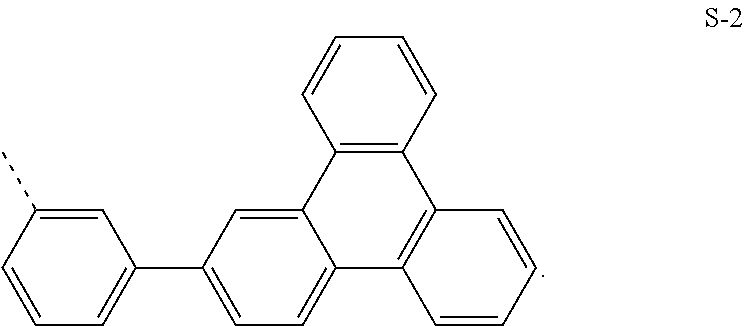


Priority Applications (1)
| Application Number | Priority Date | Filing Date | Title |
|---|---|---|---|
| US13/001,949 US8440326B2 (en) | 2008-06-30 | 2009-06-30 | Hole transport materials containing triphenylene |
Applications Claiming Priority (4)
| Application Number | Priority Date | Filing Date | Title |
|---|---|---|---|
| US7709508P | 2008-06-30 | 2008-06-30 | |
| US61077095 | 2008-06-30 | ||
| US13/001,949 US8440326B2 (en) | 2008-06-30 | 2009-06-30 | Hole transport materials containing triphenylene |
| PCT/US2009/049188 WO2010002850A1 (en) | 2008-06-30 | 2009-06-30 | Hole transport materials containing triphenylene |
Publications (2)
| Publication Number | Publication Date |
|---|---|
| US20110180786A1 US20110180786A1 (en) | 2011-07-28 |
| US8440326B2 true US8440326B2 (en) | 2013-05-14 |
Family
ID=40974592
Family Applications (1)
| Application Number | Title | Priority Date | Filing Date |
|---|---|---|---|
| US13/001,949 Active 2029-09-26 US8440326B2 (en) | 2008-06-30 | 2009-06-30 | Hole transport materials containing triphenylene |
Country Status (6)
| Country | Link |
|---|---|
| US (1) | US8440326B2 (en) |
| EP (2) | EP2860171B1 (en) |
| JP (1) | JP5591800B2 (en) |
| KR (2) | KR101778910B1 (en) |
| CN (1) | CN102131767B (en) |
| WO (1) | WO2010002850A1 (en) |
Families Citing this family (48)
| Publication number | Priority date | Publication date | Assignee | Title |
|---|---|---|---|---|
| JPH0651083A (en) * | 1992-07-28 | 1994-02-25 | Ishikawajima Harima Heavy Ind Co Ltd | Cooling device for nuclear reactor suppression pool |
| US9130177B2 (en) * | 2011-01-13 | 2015-09-08 | Universal Display Corporation | 5-substituted 2 phenylquinoline complexes materials for light emitting diode |
| JP5646733B2 (en) * | 2010-04-28 | 2014-12-24 | ユニバーサル ディスプレイ コーポレイション | Premixed material deposition |
| JP5591066B2 (en) * | 2010-10-13 | 2014-09-17 | ユー・ディー・シー アイルランド リミテッド | Organic electroluminescent device and charge transport material |
| JP5653179B2 (en) * | 2010-11-05 | 2015-01-14 | キヤノン株式会社 | Phenanthrene compound and organic light emitting device using the same |
| JP5844384B2 (en) * | 2010-12-29 | 2016-01-13 | エルジー・ケム・リミテッド | Novel compound and organic light emitting device using the same |
| JP5872944B2 (en) * | 2011-03-31 | 2016-03-01 | ユー・ディー・シー アイルランド リミテッド | Charge transport material, organic electroluminescent element, and light emitting device, display device or illumination device using the element |
| JP2014167946A (en) * | 2011-06-23 | 2014-09-11 | Toray Ind Inc | Light-emitting element |
| WO2012176675A1 (en) * | 2011-06-23 | 2012-12-27 | 東レ株式会社 | Light-emitting element |
| JPWO2013061805A1 (en) * | 2011-10-24 | 2015-04-02 | 保土谷化学工業株式会社 | Novel triphenylene derivative and organic electroluminescence device using the derivative |
| KR101968371B1 (en) | 2012-01-12 | 2019-04-11 | 유디씨 아일랜드 리미티드 | Metal complexes with dibenzo[f,h]quinoxalines |
| DE102012203466B4 (en) | 2012-03-06 | 2021-10-28 | Pictiva Displays International Limited | ORGANIC LIGHT EMITTING COMPONENT |
| JP2015115372A (en) * | 2013-12-09 | 2015-06-22 | 三星ディスプレイ株式會社Samsung Display Co.,Ltd. | Material for organic electroluminescent devices, and organic electroluminescent device using the same |
| KR20160100961A (en) | 2013-12-20 | 2016-08-24 | 바스프 에스이 | Highly efficient oled devices with very short decay times |
| EP3174885B1 (en) | 2014-07-28 | 2019-10-02 | Idemitsu Kosan Co., Ltd. | 2,9-functionalized benzimidazolo[1,2-a]benzimidazoles as hosts for organic light emitting diodes (oleds) |
| EP2982676B1 (en) | 2014-08-07 | 2018-04-11 | Idemitsu Kosan Co., Ltd. | Benzimidazo[2,1-B]benzoxazoles for electronic applications |
| EP3186264B1 (en) | 2014-08-08 | 2018-11-28 | UDC Ireland Limited | Electroluminescent imidazo-quinoxaline carbene metal complexes |
| EP2993215B1 (en) | 2014-09-04 | 2019-06-19 | Idemitsu Kosan Co., Ltd. | Azabenzimidazo[2,1-a]benzimidazoles for electronic applications |
| EP3015469B1 (en) | 2014-10-30 | 2018-12-19 | Idemitsu Kosan Co., Ltd. | 5-(benzimidazol-2-yl)benzimidazo[1,2-a]benzimidazoles for electronic applications |
| WO2016079667A1 (en) | 2014-11-17 | 2016-05-26 | Idemitsu Kosan Co., Ltd. | Indole derivatives for electronic applications |
| WO2016079169A1 (en) | 2014-11-18 | 2016-05-26 | Basf Se | Pt- or pd-carbene complexes for use in organic light emitting diodes |
| EP3034506A1 (en) | 2014-12-15 | 2016-06-22 | Idemitsu Kosan Co., Ltd | 4-functionalized carbazole derivatives for electronic applications |
| EP3034507A1 (en) | 2014-12-15 | 2016-06-22 | Idemitsu Kosan Co., Ltd | 1-functionalized dibenzofurans and dibenzothiophenes for organic light emitting diodes (OLEDs) |
| EP3054498B1 (en) | 2015-02-06 | 2017-09-20 | Idemitsu Kosan Co., Ltd. | Bisimidazodiazocines |
| EP3053918B1 (en) | 2015-02-06 | 2018-04-11 | Idemitsu Kosan Co., Ltd. | 2-carbazole substituted benzimidazoles for electronic applications |
| US9812649B2 (en) | 2015-02-17 | 2017-11-07 | Luminescence Technology Corp. | Indenotriphenylene-based amine derivative for organic electroluminescent device |
| EP3061759B1 (en) | 2015-02-24 | 2019-12-25 | Idemitsu Kosan Co., Ltd | Nitrile substituted dibenzofurans |
| EP3070144B1 (en) | 2015-03-17 | 2018-02-28 | Idemitsu Kosan Co., Ltd. | Seven-membered ring compounds |
| EP3072943B1 (en) | 2015-03-26 | 2018-05-02 | Idemitsu Kosan Co., Ltd. | Dibenzofuran/carbazole-substituted benzonitriles |
| EP3075737B1 (en) | 2015-03-31 | 2019-12-04 | Idemitsu Kosan Co., Ltd | Benzimidazolo[1,2-a]benzimidazole carrying aryl- or heteroarylnitril groups for organic light emitting diodes |
| US9698351B2 (en) * | 2015-04-29 | 2017-07-04 | Feng-wen Yen | Organic material for electroluminescent device |
| US10014478B2 (en) * | 2015-05-19 | 2018-07-03 | Feng-wen Yen | Indenotriphenylene-based diamine derivative and organic electroluminescence device using the same |
| CN111668392B (en) | 2015-06-03 | 2024-01-23 | Udc 爱尔兰有限责任公司 | High efficiency OLED device with extremely short decay time |
| WO2017056055A1 (en) | 2015-10-01 | 2017-04-06 | Idemitsu Kosan Co., Ltd. | Benzimidazolo[1,2-a]benzimidazole carrying triazine groups for organic light emitting diodes |
| EP3356368B1 (en) | 2015-10-01 | 2021-07-21 | Idemitsu Kosan Co., Ltd | Benzimidazolo[1,2-a]benzimidazole carrying benzimidazolo[1,2-a]benzimidazolyl groups, carbazolyl groups, benzofurane groups or benzothiophene groups for organic light emitting diodes |
| EP3150604B1 (en) | 2015-10-01 | 2021-07-14 | Idemitsu Kosan Co., Ltd. | Benzimidazolo[1,2-a]benzimidazole carrying benzimidazolo[1,2-a]benzimidazolylyl groups, carbazolyl groups, benzofurane groups or benzothiophene groups for organic light emitting diodes |
| EP3150606B1 (en) | 2015-10-01 | 2019-08-14 | Idemitsu Kosan Co., Ltd. | Benzimidazolo[1,2-a]benzimidazoles carrying benzofurane or benzothiophene groups for organic light emitting diodes |
| CN108349987A (en) | 2015-11-04 | 2018-07-31 | 出光兴产株式会社 | Benzimidazole fused heteroaromatics |
| US11174258B2 (en) | 2015-12-04 | 2021-11-16 | Idemitsu Kosan Co., Ltd. | Benzimidazolo[1,2-a]benzimidazole derivatives for organic light emitting diodes |
| KR20170074170A (en) | 2015-12-21 | 2017-06-29 | 유디씨 아일랜드 리미티드 | Transition metal complexes with tripodal ligands and the use thereof in oleds |
| EP3394062B1 (en) | 2015-12-21 | 2019-10-02 | Idemitsu Kosan Co., Ltd | Hetero-condensed phenylquinazolines and their use in electronic devices |
| US10968229B2 (en) | 2016-04-12 | 2021-04-06 | Idemitsu Kosan Co., Ltd. | Seven-membered ring compounds |
| CN105949443B (en) * | 2016-04-21 | 2019-04-05 | 复旦大学 | A kind of azepine condensed ring aromatic hydrocarbons stephanoporate framework of two-dimensional slice structure and its preparation method and application |
| EP3418285B1 (en) | 2017-06-20 | 2020-05-06 | Idemitsu Kosan Co., Ltd. | Composition comprising a substituted ir complex and a phenylquinazoline bridged with a heteroatom |
| EP3466954A1 (en) | 2017-10-04 | 2019-04-10 | Idemitsu Kosan Co., Ltd. | Fused phenylquinazolines bridged with a heteroatom |
| CN109627175A (en) * | 2017-10-09 | 2019-04-16 | 北京夏禾科技有限公司 | Cross-linking deuterated charge transport compound, organic electroluminescence device and solution formula comprising the compound |
| CN107814726B (en) * | 2017-10-31 | 2020-02-07 | 长春海谱润斯科技有限公司 | Organic compound containing fluorene and organic light-emitting device thereof |
| CN109400488A (en) * | 2018-11-29 | 2019-03-01 | 长春海谱润斯科技有限公司 | A kind of aromatic amino-derivative and its organic electroluminescence device |
Citations (99)
| Publication number | Priority date | Publication date | Assignee | Title |
|---|---|---|---|---|
| US4769292A (en) | 1987-03-02 | 1988-09-06 | Eastman Kodak Company | Electroluminescent device with modified thin film luminescent zone |
| US5061569A (en) | 1990-07-26 | 1991-10-29 | Eastman Kodak Company | Electroluminescent device with organic electroluminescent medium |
| US5247190A (en) | 1989-04-20 | 1993-09-21 | Cambridge Research And Innovation Limited | Electroluminescent devices |
| EP0650955A1 (en) | 1993-11-01 | 1995-05-03 | Hodogaya Chemical Co., Ltd. | Amine compound and electro-luminescence device comprising same |
| US5703436A (en) | 1994-12-13 | 1997-12-30 | The Trustees Of Princeton University | Transparent contacts for organic devices |
| US5707745A (en) | 1994-12-13 | 1998-01-13 | The Trustees Of Princeton University | Multicolor organic light emitting devices |
| US5834893A (en) | 1996-12-23 | 1998-11-10 | The Trustees Of Princeton University | High efficiency organic light emitting devices with light directing structures |
| US5844363A (en) | 1997-01-23 | 1998-12-01 | The Trustees Of Princeton Univ. | Vacuum deposited, non-polymeric flexible organic light emitting devices |
| US6013982A (en) | 1996-12-23 | 2000-01-11 | The Trustees Of Princeton University | Multicolor display devices |
| US6087196A (en) | 1998-01-30 | 2000-07-11 | The Trustees Of Princeton University | Fabrication of organic semiconductor devices using ink jet printing |
| US6091195A (en) | 1997-02-03 | 2000-07-18 | The Trustees Of Princeton University | Displays having mesa pixel configuration |
| US6097147A (en) | 1998-09-14 | 2000-08-01 | The Trustees Of Princeton University | Structure for high efficiency electroluminescent device |
| JP2000299497A (en) | 1999-02-09 | 2000-10-24 | Nichia Chem Ind Ltd | Nitride semiconductor element |
| WO2001039234A2 (en) | 1999-11-24 | 2001-05-31 | The Trustees Of Princeton University | Organic light emitting diode having a blue phosphorescent molecule as an emitter |
| US6294398B1 (en) | 1999-11-23 | 2001-09-25 | The Trustees Of Princeton University | Method for patterning devices |
| US6303238B1 (en) | 1997-12-01 | 2001-10-16 | The Trustees Of Princeton University | OLEDs doped with phosphorescent compounds |
| US6337102B1 (en) | 1997-11-17 | 2002-01-08 | The Trustees Of Princeton University | Low pressure vapor phase deposition of organic thin films |
| WO2002002714A2 (en) | 2000-06-30 | 2002-01-10 | E.I. Du Pont De Nemours And Company | Electroluminescent iridium compounds with fluorinated phenylpyridines, phenylpyrimidines, and phenylquinolines and devices made with such compounds |
| WO2002015645A1 (en) | 2000-08-11 | 2002-02-21 | The Trustees Of Princeton University | Organometallic compounds and emission-shifting organic electrophosphorescence |
| US20020034656A1 (en) | 1998-09-14 | 2002-03-21 | Thompson Mark E. | Organometallic complexes as phosphorescent emitters in organic LEDs |
| US20020134984A1 (en) | 2001-02-01 | 2002-09-26 | Fuji Photo Film Co., Ltd. | Transition metal complex and light-emitting device |
| US20020158242A1 (en) | 1999-12-31 | 2002-10-31 | Se-Hwan Son | Electronic device comprising organic compound having p-type semiconducting characteristics |
| US6528187B1 (en) | 1998-09-08 | 2003-03-04 | Fuji Photo Film Co., Ltd. | Material for luminescence element and luminescence element using the same |
| WO2003040257A1 (en) | 2001-11-07 | 2003-05-15 | E. I. Du Pont De Nemours And Company | Electroluminescent platinum compounds and devices made with such compounds |
| US20030138657A1 (en) | 2000-12-07 | 2003-07-24 | Canon Kabushiki Kaisha | Deuterated semi-conducting organic compounds used for opto-electronic devices |
| WO2003060956A2 (en) | 2002-01-18 | 2003-07-24 | Lg Chem, Ltd. | New material for transporting electrons and organic electroluminescent display using the same |
| US20030152802A1 (en) | 2001-06-19 | 2003-08-14 | Akira Tsuboyama | Metal coordination compound and organic liminescence device |
| US20030162053A1 (en) | 1996-06-25 | 2003-08-28 | Marks Tobin J. | Organic light - emitting diodes and methods for assembly and enhanced charge injection |
| US20030175553A1 (en) | 2001-12-28 | 2003-09-18 | Thompson Mark E. | White light emitting oleds from combined monomer and aggregate emission |
| US20030230980A1 (en) | 2002-06-18 | 2003-12-18 | Forrest Stephen R | Very low voltage, high efficiency phosphorescent oled in a p-i-n structure |
| US6687266B1 (en) | 2002-11-08 | 2004-02-03 | Universal Display Corporation | Organic light emitting materials and devices |
| US20040036077A1 (en) | 2002-08-22 | 2004-02-26 | Fuji Photo Film Co., Ltd. | Light emitting element |
| US20040137268A1 (en) | 2002-12-27 | 2004-07-15 | Fuji Photo Film Co., Ltd. | Organic electroluminescent device |
| US20040137267A1 (en) | 2002-12-27 | 2004-07-15 | Fuji Photo Film Co., Ltd. | Organic electroluminescent device |
| US20040174116A1 (en) | 2001-08-20 | 2004-09-09 | Lu Min-Hao Michael | Transparent electrodes |
| WO2004093207A2 (en) | 2003-04-15 | 2004-10-28 | Covion Organic Semiconductors Gmbh | Mixtures of matrix materials and organic semiconductors capable of emission, use of the same and electronic components containing said mixtures |
| WO2004107822A1 (en) | 2003-05-29 | 2004-12-09 | Nippon Steel Chemical Co., Ltd. | Organic electroluminescent element |
| US6835469B2 (en) | 2001-10-17 | 2004-12-28 | The University Of Southern California | Phosphorescent compounds and devices comprising the same |
| JP2005011610A (en) | 2003-06-18 | 2005-01-13 | Nippon Steel Chem Co Ltd | Organic electroluminescent element |
| US20050025993A1 (en) | 2003-07-25 | 2005-02-03 | Thompson Mark E. | Materials and structures for enhancing the performance of organic light emitting devices |
| WO2005014551A1 (en) | 2003-08-07 | 2005-02-17 | Nippon Steel Chemical Co., Ltd. | Aluminum chelate compelx for organic el material |
| WO2005019373A2 (en) | 2003-08-19 | 2005-03-03 | Basf Aktiengesellschaft | Transition metal complexes comprising carbene ligands serving as emitters for organic light-emitting diodes (oled's) |
| JP2005071983A (en) * | 2003-08-04 | 2005-03-17 | Fuji Photo Film Co Ltd | Organic electroluminescent device |
| WO2005030900A1 (en) | 2003-09-25 | 2005-04-07 | Nippon Steel Chemical Co., Ltd. | Organic electroluminescent device |
| US20050112407A1 (en) | 2003-11-21 | 2005-05-26 | Fuji Photo Film Co., Ltd. | Organic electroluminescent device |
| US6921915B2 (en) | 2001-03-08 | 2005-07-26 | Canon Kabushiki Kaisha | Metal coordination compound, luminescence device and display apparatus |
| WO2005089025A1 (en) | 2004-03-15 | 2005-09-22 | Nippon Steel Chemical Co., Ltd. | Organic electroluminescent device |
| US20050238919A1 (en) | 2004-04-23 | 2005-10-27 | Fuji Photo Film Co., Ltd. | Organic electroluminescent device |
| US20050244673A1 (en) | 2002-08-27 | 2005-11-03 | Fujitsu Limited | Organometallic complex, organic EL element and organic EL display |
| US20050260441A1 (en) | 2004-05-18 | 2005-11-24 | Thompson Mark E | Luminescent compounds with carbene ligands |
| US20050260449A1 (en) | 2004-05-18 | 2005-11-24 | Robert Walters | Complexes with tridentate ligands |
| WO2005123873A1 (en) | 2004-06-17 | 2005-12-29 | Konica Minolta Holdings, Inc. | Organic electroluminescent device material, organic electroluminescent device, display and illuminating device |
| US20060008670A1 (en) | 2004-07-06 | 2006-01-12 | Chun Lin | Organic light emitting materials and devices |
| WO2006009024A1 (en) | 2004-07-23 | 2006-01-26 | Konica Minolta Holdings, Inc. | Organic electroluminescent device, display and illuminating device |
| US20060088728A1 (en) | 2004-10-22 | 2006-04-27 | Raymond Kwong | Arylcarbazoles as hosts in PHOLEDs |
| US7087321B2 (en) | 2003-04-22 | 2006-08-08 | Universal Display Corporation | Organic light emitting devices having reduced pixel shrinkage |
| US7090928B2 (en) | 2003-04-01 | 2006-08-15 | The University Of Southern California | Binuclear compounds |
| US20060202194A1 (en) | 2005-03-08 | 2006-09-14 | Jeong Hyun C | Red phosphorescene compounds and organic electroluminescence device using the same |
| US20060240279A1 (en) | 2005-04-21 | 2006-10-26 | Vadim Adamovich | Non-blocked phosphorescent OLEDs |
| US20060251923A1 (en) | 2005-05-06 | 2006-11-09 | Chun Lin | Stability OLED materials and devices |
| EP1725079A1 (en) | 2004-03-11 | 2006-11-22 | Mitsubishi Chemical Corporation | Composition for charge-transporting film and ion compound, charge-transporting film and organic electroluminescent device using same, and method for manufacturing organic electroluminescent device and method for producing charge-transporting film |
| US20060263635A1 (en) | 2005-05-06 | 2006-11-23 | Fuji Photo Film Co., Ltd. | Organic electroluminescent device |
| US20060280965A1 (en) * | 2005-05-31 | 2006-12-14 | Raymond Kwong | Triphenylene hosts in phosphorescent light emitting diodes |
| US7154114B2 (en) | 2004-05-18 | 2006-12-26 | Universal Display Corporation | Cyclometallated iridium carbene complexes for use as hosts |
| US20070088167A1 (en) | 2005-05-06 | 2007-04-19 | Chun Lin | Stability OLED materials and devices |
| JP2007123392A (en) | 2005-10-26 | 2007-05-17 | Konica Minolta Holdings Inc | Organic electroluminescence device, display device and lighting device |
| US7250226B2 (en) | 2001-08-31 | 2007-07-31 | Nippon Hoso Kyokai | Phosphorescent compound, a phosphorescent composition and an organic light-emitting device |
| US20070190359A1 (en) | 2006-02-10 | 2007-08-16 | Knowles David B | Metal complexes of cyclometallated imidazo[1,2-ƒ]phenanthridine and diimidazo[1,2-a:1',2'-c]quinazoline ligands and isoelectronic and benzannulated analogs thereof |
| JP2007254297A (en) | 2006-03-20 | 2007-10-04 | Nippon Steel Chem Co Ltd | Compound of light-emitting layer and organic electroluminescent device |
| US20070278938A1 (en) | 2006-04-26 | 2007-12-06 | Idemitsu Kosan Co., Ltd. | Aromatic amine derivative and electroluminescence device using the same |
| US20080015355A1 (en) | 2004-06-28 | 2008-01-17 | Thomas Schafer | Electroluminescent Metal Complexes With Triazoles And Benzotriazoles |
| US20080018221A1 (en) | 2004-11-25 | 2008-01-24 | Basf Aktiengesellschaft | Use Of Transition Metal Carbene Complexes In Organic Light-Emitting Diodes (Oleds) |
| US7332232B2 (en) | 2004-02-03 | 2008-02-19 | Universal Display Corporation | OLEDs utilizing multidentate ligand systems |
| US7338722B2 (en) | 2003-03-24 | 2008-03-04 | The University Of Southern California | Phenyl and fluorenyl substituted phenyl-pyrazole complexes of Ir |
| JP2008074939A (en) | 2006-09-21 | 2008-04-03 | Konica Minolta Holdings Inc | Organic electroluminescence element material, organic electroluminescence element, display device and illumination device |
| US20080106190A1 (en) | 2006-08-23 | 2008-05-08 | Idemitsu Kosan Co., Ltd. | Aromatic amine derivatives and organic electroluminescent device using same |
| US20080124572A1 (en) | 2006-11-24 | 2008-05-29 | Idemitsu Kosan Co., Ltd. | Aromatic amine derivative and organic electroluminescence device using the same |
| US7393599B2 (en) | 2004-05-18 | 2008-07-01 | The University Of Southern California | Luminescent compounds with carbene ligands |
| US7396598B2 (en) | 2001-06-20 | 2008-07-08 | Showa Denko K.K. | Light emitting material and organic light-emitting device |
| US20080220265A1 (en) | 2006-12-08 | 2008-09-11 | Universal Display Corporation | Cross-linkable Iridium Complexes and Organic Light-Emitting Devices Using the Same |
| US7431968B1 (en) | 2001-09-04 | 2008-10-07 | The Trustees Of Princeton University | Process and apparatus for organic vapor jet deposition |
| US20080261076A1 (en) | 2007-03-08 | 2008-10-23 | Universal Display Corporation | Phosphorescent materials |
| US7445855B2 (en) | 2004-05-18 | 2008-11-04 | The University Of Southern California | Cationic metal-carbene complexes |
| US20080297033A1 (en) | 2006-02-10 | 2008-12-04 | Knowles David B | Blue phosphorescent imidazophenanthridine materials |
| US20090008605A1 (en) | 2007-07-07 | 2009-01-08 | Idemitsu Kosan Co., Ltd. | Naphthalene derivative, material for organic electroluminescence device, and organic electroluminescence device using the same |
| US20090009065A1 (en) | 2007-07-07 | 2009-01-08 | Idemitsu Kosan Co., Ltd. | Organic electroluminescence device and material for organic electroluminescence device |
| US20090017330A1 (en) | 2007-07-10 | 2009-01-15 | Idemitsu Kosan Co., Ltd. | Material for organic electroluminescence device and organic electroluminescence device utilizing the same |
| US20090030202A1 (en) | 2007-07-10 | 2009-01-29 | Idemitsu Kosan Co., Ltd. | Material for organic electroluminescent element and organic electroluminescent element employing the same |
| US20090039776A1 (en) | 2007-08-09 | 2009-02-12 | Canon Kabushiki Kaisha | Organometallic complex and organic light-emitting element using same |
| US20090045731A1 (en) | 2007-07-07 | 2009-02-19 | Idemitsu Kosan Co., Ltd. | Organic electroluminescence device and material for organic electroluminescence device |
| US20090045730A1 (en) | 2007-07-07 | 2009-02-19 | Idemitsu Kosan Co., Ltd. | Organic electroluminescence device and material for organic electroluminescence device |
| EP2034538A1 (en) | 2006-06-02 | 2009-03-11 | Idemitsu Kosan Co., Ltd. | Material for organic electroluminescence element, and organic electroluminescence element using the material |
| US20090101870A1 (en) | 2007-10-22 | 2009-04-23 | E. I. Du Pont De Nemours And Company | Electron transport bi-layers and devices made with such bi-layers |
| US20090108737A1 (en) | 2006-12-08 | 2009-04-30 | Raymond Kwong | Light-emitting organometallic complexes |
| US20090115316A1 (en) | 2007-11-02 | 2009-05-07 | Shiying Zheng | Organic electroluminescent device having an azatriphenylene derivative |
| US7534505B2 (en) | 2004-05-18 | 2009-05-19 | The University Of Southern California | Organometallic compounds for use in electroluminescent devices |
| US20090165846A1 (en) | 2005-09-07 | 2009-07-02 | Universitaet Braunschweig | Triplet emitter having condensed five-membered rings |
| US20090167162A1 (en) | 2007-12-28 | 2009-07-02 | Universal Display Corporation | Dibenzothiophene-containing materials in phosphorescent light emitting diodes |
| US20090179554A1 (en) | 2006-05-11 | 2009-07-16 | Hitoshi Kuma | Organic electroluminescent device |
Family Cites Families (4)
| Publication number | Priority date | Publication date | Assignee | Title |
|---|---|---|---|---|
| US1339107A (en) | 1918-08-28 | 1920-05-04 | Elmer C Dittmar | Apparatus for coating and finishing flooring |
| US4423408A (en) | 1981-02-09 | 1983-12-27 | Honeywell Inc. | Remote data gathering panel |
| JP4906235B2 (en) * | 2004-03-10 | 2012-03-28 | 富士フイルム株式会社 | Organic electroluminescence device |
| US7421968B1 (en) * | 2007-02-20 | 2008-09-09 | Yen-Lu Hu | Boat that is provided with floating tubes in a multi-layer design |
-
2009
- 2009-06-30 JP JP2011516801A patent/JP5591800B2/en active Active
- 2009-06-30 EP EP14194736.6A patent/EP2860171B1/en active Active
- 2009-06-30 WO PCT/US2009/049188 patent/WO2010002850A1/en active Application Filing
- 2009-06-30 CN CN2009801324876A patent/CN102131767B/en active Active
- 2009-06-30 KR KR1020167030066A patent/KR101778910B1/en active IP Right Grant
- 2009-06-30 KR KR1020117001066A patent/KR101676501B1/en active IP Right Grant
- 2009-06-30 EP EP09774301.7A patent/EP2313362B1/en active Active
- 2009-06-30 US US13/001,949 patent/US8440326B2/en active Active
Patent Citations (101)
| Publication number | Priority date | Publication date | Assignee | Title |
|---|---|---|---|---|
| US4769292A (en) | 1987-03-02 | 1988-09-06 | Eastman Kodak Company | Electroluminescent device with modified thin film luminescent zone |
| US5247190A (en) | 1989-04-20 | 1993-09-21 | Cambridge Research And Innovation Limited | Electroluminescent devices |
| US5061569A (en) | 1990-07-26 | 1991-10-29 | Eastman Kodak Company | Electroluminescent device with organic electroluminescent medium |
| EP0650955A1 (en) | 1993-11-01 | 1995-05-03 | Hodogaya Chemical Co., Ltd. | Amine compound and electro-luminescence device comprising same |
| US5703436A (en) | 1994-12-13 | 1997-12-30 | The Trustees Of Princeton University | Transparent contacts for organic devices |
| US5707745A (en) | 1994-12-13 | 1998-01-13 | The Trustees Of Princeton University | Multicolor organic light emitting devices |
| US20030162053A1 (en) | 1996-06-25 | 2003-08-28 | Marks Tobin J. | Organic light - emitting diodes and methods for assembly and enhanced charge injection |
| US6013982A (en) | 1996-12-23 | 2000-01-11 | The Trustees Of Princeton University | Multicolor display devices |
| US5834893A (en) | 1996-12-23 | 1998-11-10 | The Trustees Of Princeton University | High efficiency organic light emitting devices with light directing structures |
| US5844363A (en) | 1997-01-23 | 1998-12-01 | The Trustees Of Princeton Univ. | Vacuum deposited, non-polymeric flexible organic light emitting devices |
| US6091195A (en) | 1997-02-03 | 2000-07-18 | The Trustees Of Princeton University | Displays having mesa pixel configuration |
| US6337102B1 (en) | 1997-11-17 | 2002-01-08 | The Trustees Of Princeton University | Low pressure vapor phase deposition of organic thin films |
| US6303238B1 (en) | 1997-12-01 | 2001-10-16 | The Trustees Of Princeton University | OLEDs doped with phosphorescent compounds |
| US6087196A (en) | 1998-01-30 | 2000-07-11 | The Trustees Of Princeton University | Fabrication of organic semiconductor devices using ink jet printing |
| US6528187B1 (en) | 1998-09-08 | 2003-03-04 | Fuji Photo Film Co., Ltd. | Material for luminescence element and luminescence element using the same |
| US6097147A (en) | 1998-09-14 | 2000-08-01 | The Trustees Of Princeton University | Structure for high efficiency electroluminescent device |
| US20020034656A1 (en) | 1998-09-14 | 2002-03-21 | Thompson Mark E. | Organometallic complexes as phosphorescent emitters in organic LEDs |
| JP2000299497A (en) | 1999-02-09 | 2000-10-24 | Nichia Chem Ind Ltd | Nitride semiconductor element |
| US6468819B1 (en) | 1999-11-23 | 2002-10-22 | The Trustees Of Princeton University | Method for patterning organic thin film devices using a die |
| US6294398B1 (en) | 1999-11-23 | 2001-09-25 | The Trustees Of Princeton University | Method for patterning devices |
| WO2001039234A2 (en) | 1999-11-24 | 2001-05-31 | The Trustees Of Princeton University | Organic light emitting diode having a blue phosphorescent molecule as an emitter |
| US20020158242A1 (en) | 1999-12-31 | 2002-10-31 | Se-Hwan Son | Electronic device comprising organic compound having p-type semiconducting characteristics |
| WO2002002714A2 (en) | 2000-06-30 | 2002-01-10 | E.I. Du Pont De Nemours And Company | Electroluminescent iridium compounds with fluorinated phenylpyridines, phenylpyrimidines, and phenylquinolines and devices made with such compounds |
| WO2002015645A1 (en) | 2000-08-11 | 2002-02-21 | The Trustees Of Princeton University | Organometallic compounds and emission-shifting organic electrophosphorescence |
| US20030138657A1 (en) | 2000-12-07 | 2003-07-24 | Canon Kabushiki Kaisha | Deuterated semi-conducting organic compounds used for opto-electronic devices |
| US20020134984A1 (en) | 2001-02-01 | 2002-09-26 | Fuji Photo Film Co., Ltd. | Transition metal complex and light-emitting device |
| US6921915B2 (en) | 2001-03-08 | 2005-07-26 | Canon Kabushiki Kaisha | Metal coordination compound, luminescence device and display apparatus |
| US20030152802A1 (en) | 2001-06-19 | 2003-08-14 | Akira Tsuboyama | Metal coordination compound and organic liminescence device |
| US7396598B2 (en) | 2001-06-20 | 2008-07-08 | Showa Denko K.K. | Light emitting material and organic light-emitting device |
| US20040174116A1 (en) | 2001-08-20 | 2004-09-09 | Lu Min-Hao Michael | Transparent electrodes |
| US7250226B2 (en) | 2001-08-31 | 2007-07-31 | Nippon Hoso Kyokai | Phosphorescent compound, a phosphorescent composition and an organic light-emitting device |
| US7431968B1 (en) | 2001-09-04 | 2008-10-07 | The Trustees Of Princeton University | Process and apparatus for organic vapor jet deposition |
| US6835469B2 (en) | 2001-10-17 | 2004-12-28 | The University Of Southern California | Phosphorescent compounds and devices comprising the same |
| WO2003040257A1 (en) | 2001-11-07 | 2003-05-15 | E. I. Du Pont De Nemours And Company | Electroluminescent platinum compounds and devices made with such compounds |
| US20030175553A1 (en) | 2001-12-28 | 2003-09-18 | Thompson Mark E. | White light emitting oleds from combined monomer and aggregate emission |
| WO2003060956A2 (en) | 2002-01-18 | 2003-07-24 | Lg Chem, Ltd. | New material for transporting electrons and organic electroluminescent display using the same |
| US20030230980A1 (en) | 2002-06-18 | 2003-12-18 | Forrest Stephen R | Very low voltage, high efficiency phosphorescent oled in a p-i-n structure |
| US20040036077A1 (en) | 2002-08-22 | 2004-02-26 | Fuji Photo Film Co., Ltd. | Light emitting element |
| US20050244673A1 (en) | 2002-08-27 | 2005-11-03 | Fujitsu Limited | Organometallic complex, organic EL element and organic EL display |
| US6687266B1 (en) | 2002-11-08 | 2004-02-03 | Universal Display Corporation | Organic light emitting materials and devices |
| US20040137267A1 (en) | 2002-12-27 | 2004-07-15 | Fuji Photo Film Co., Ltd. | Organic electroluminescent device |
| US20040137268A1 (en) | 2002-12-27 | 2004-07-15 | Fuji Photo Film Co., Ltd. | Organic electroluminescent device |
| US7338722B2 (en) | 2003-03-24 | 2008-03-04 | The University Of Southern California | Phenyl and fluorenyl substituted phenyl-pyrazole complexes of Ir |
| US7090928B2 (en) | 2003-04-01 | 2006-08-15 | The University Of Southern California | Binuclear compounds |
| WO2004093207A2 (en) | 2003-04-15 | 2004-10-28 | Covion Organic Semiconductors Gmbh | Mixtures of matrix materials and organic semiconductors capable of emission, use of the same and electronic components containing said mixtures |
| US7087321B2 (en) | 2003-04-22 | 2006-08-08 | Universal Display Corporation | Organic light emitting devices having reduced pixel shrinkage |
| WO2004107822A1 (en) | 2003-05-29 | 2004-12-09 | Nippon Steel Chemical Co., Ltd. | Organic electroluminescent element |
| JP2005011610A (en) | 2003-06-18 | 2005-01-13 | Nippon Steel Chem Co Ltd | Organic electroluminescent element |
| US20050025993A1 (en) | 2003-07-25 | 2005-02-03 | Thompson Mark E. | Materials and structures for enhancing the performance of organic light emitting devices |
| JP2005071983A (en) * | 2003-08-04 | 2005-03-17 | Fuji Photo Film Co Ltd | Organic electroluminescent device |
| WO2005014551A1 (en) | 2003-08-07 | 2005-02-17 | Nippon Steel Chemical Co., Ltd. | Aluminum chelate compelx for organic el material |
| WO2005019373A2 (en) | 2003-08-19 | 2005-03-03 | Basf Aktiengesellschaft | Transition metal complexes comprising carbene ligands serving as emitters for organic light-emitting diodes (oled's) |
| WO2005030900A1 (en) | 2003-09-25 | 2005-04-07 | Nippon Steel Chemical Co., Ltd. | Organic electroluminescent device |
| US20050112407A1 (en) | 2003-11-21 | 2005-05-26 | Fuji Photo Film Co., Ltd. | Organic electroluminescent device |
| US7332232B2 (en) | 2004-02-03 | 2008-02-19 | Universal Display Corporation | OLEDs utilizing multidentate ligand systems |
| EP1725079A1 (en) | 2004-03-11 | 2006-11-22 | Mitsubishi Chemical Corporation | Composition for charge-transporting film and ion compound, charge-transporting film and organic electroluminescent device using same, and method for manufacturing organic electroluminescent device and method for producing charge-transporting film |
| WO2005089025A1 (en) | 2004-03-15 | 2005-09-22 | Nippon Steel Chemical Co., Ltd. | Organic electroluminescent device |
| US20050238919A1 (en) | 2004-04-23 | 2005-10-27 | Fuji Photo Film Co., Ltd. | Organic electroluminescent device |
| US7534505B2 (en) | 2004-05-18 | 2009-05-19 | The University Of Southern California | Organometallic compounds for use in electroluminescent devices |
| US7393599B2 (en) | 2004-05-18 | 2008-07-01 | The University Of Southern California | Luminescent compounds with carbene ligands |
| US20050260441A1 (en) | 2004-05-18 | 2005-11-24 | Thompson Mark E | Luminescent compounds with carbene ligands |
| US20050260449A1 (en) | 2004-05-18 | 2005-11-24 | Robert Walters | Complexes with tridentate ligands |
| US7445855B2 (en) | 2004-05-18 | 2008-11-04 | The University Of Southern California | Cationic metal-carbene complexes |
| US7279704B2 (en) | 2004-05-18 | 2007-10-09 | The University Of Southern California | Complexes with tridentate ligands |
| US7154114B2 (en) | 2004-05-18 | 2006-12-26 | Universal Display Corporation | Cyclometallated iridium carbene complexes for use as hosts |
| WO2005123873A1 (en) | 2004-06-17 | 2005-12-29 | Konica Minolta Holdings, Inc. | Organic electroluminescent device material, organic electroluminescent device, display and illuminating device |
| US20080015355A1 (en) | 2004-06-28 | 2008-01-17 | Thomas Schafer | Electroluminescent Metal Complexes With Triazoles And Benzotriazoles |
| US20060008670A1 (en) | 2004-07-06 | 2006-01-12 | Chun Lin | Organic light emitting materials and devices |
| WO2006009024A1 (en) | 2004-07-23 | 2006-01-26 | Konica Minolta Holdings, Inc. | Organic electroluminescent device, display and illuminating device |
| US20060088728A1 (en) | 2004-10-22 | 2006-04-27 | Raymond Kwong | Arylcarbazoles as hosts in PHOLEDs |
| US20080018221A1 (en) | 2004-11-25 | 2008-01-24 | Basf Aktiengesellschaft | Use Of Transition Metal Carbene Complexes In Organic Light-Emitting Diodes (Oleds) |
| US20060202194A1 (en) | 2005-03-08 | 2006-09-14 | Jeong Hyun C | Red phosphorescene compounds and organic electroluminescence device using the same |
| US20060240279A1 (en) | 2005-04-21 | 2006-10-26 | Vadim Adamovich | Non-blocked phosphorescent OLEDs |
| US20060263635A1 (en) | 2005-05-06 | 2006-11-23 | Fuji Photo Film Co., Ltd. | Organic electroluminescent device |
| US20060251923A1 (en) | 2005-05-06 | 2006-11-09 | Chun Lin | Stability OLED materials and devices |
| US20070088167A1 (en) | 2005-05-06 | 2007-04-19 | Chun Lin | Stability OLED materials and devices |
| US20060280965A1 (en) * | 2005-05-31 | 2006-12-14 | Raymond Kwong | Triphenylene hosts in phosphorescent light emitting diodes |
| US20090165846A1 (en) | 2005-09-07 | 2009-07-02 | Universitaet Braunschweig | Triplet emitter having condensed five-membered rings |
| JP2007123392A (en) | 2005-10-26 | 2007-05-17 | Konica Minolta Holdings Inc | Organic electroluminescence device, display device and lighting device |
| US20080297033A1 (en) | 2006-02-10 | 2008-12-04 | Knowles David B | Blue phosphorescent imidazophenanthridine materials |
| US20070190359A1 (en) | 2006-02-10 | 2007-08-16 | Knowles David B | Metal complexes of cyclometallated imidazo[1,2-ƒ]phenanthridine and diimidazo[1,2-a:1',2'-c]quinazoline ligands and isoelectronic and benzannulated analogs thereof |
| JP2007254297A (en) | 2006-03-20 | 2007-10-04 | Nippon Steel Chem Co Ltd | Compound of light-emitting layer and organic electroluminescent device |
| US20070278938A1 (en) | 2006-04-26 | 2007-12-06 | Idemitsu Kosan Co., Ltd. | Aromatic amine derivative and electroluminescence device using the same |
| US20090179554A1 (en) | 2006-05-11 | 2009-07-16 | Hitoshi Kuma | Organic electroluminescent device |
| EP2034538A1 (en) | 2006-06-02 | 2009-03-11 | Idemitsu Kosan Co., Ltd. | Material for organic electroluminescence element, and organic electroluminescence element using the material |
| US20080106190A1 (en) | 2006-08-23 | 2008-05-08 | Idemitsu Kosan Co., Ltd. | Aromatic amine derivatives and organic electroluminescent device using same |
| JP2008074939A (en) | 2006-09-21 | 2008-04-03 | Konica Minolta Holdings Inc | Organic electroluminescence element material, organic electroluminescence element, display device and illumination device |
| US20080124572A1 (en) | 2006-11-24 | 2008-05-29 | Idemitsu Kosan Co., Ltd. | Aromatic amine derivative and organic electroluminescence device using the same |
| US20080220265A1 (en) | 2006-12-08 | 2008-09-11 | Universal Display Corporation | Cross-linkable Iridium Complexes and Organic Light-Emitting Devices Using the Same |
| US20090108737A1 (en) | 2006-12-08 | 2009-04-30 | Raymond Kwong | Light-emitting organometallic complexes |
| US20080261076A1 (en) | 2007-03-08 | 2008-10-23 | Universal Display Corporation | Phosphorescent materials |
| US20090045730A1 (en) | 2007-07-07 | 2009-02-19 | Idemitsu Kosan Co., Ltd. | Organic electroluminescence device and material for organic electroluminescence device |
| US20090008605A1 (en) | 2007-07-07 | 2009-01-08 | Idemitsu Kosan Co., Ltd. | Naphthalene derivative, material for organic electroluminescence device, and organic electroluminescence device using the same |
| US20090045731A1 (en) | 2007-07-07 | 2009-02-19 | Idemitsu Kosan Co., Ltd. | Organic electroluminescence device and material for organic electroluminescence device |
| US20090009065A1 (en) | 2007-07-07 | 2009-01-08 | Idemitsu Kosan Co., Ltd. | Organic electroluminescence device and material for organic electroluminescence device |
| US20090030202A1 (en) | 2007-07-10 | 2009-01-29 | Idemitsu Kosan Co., Ltd. | Material for organic electroluminescent element and organic electroluminescent element employing the same |
| US20090017330A1 (en) | 2007-07-10 | 2009-01-15 | Idemitsu Kosan Co., Ltd. | Material for organic electroluminescence device and organic electroluminescence device utilizing the same |
| US20090039776A1 (en) | 2007-08-09 | 2009-02-12 | Canon Kabushiki Kaisha | Organometallic complex and organic light-emitting element using same |
| US20090101870A1 (en) | 2007-10-22 | 2009-04-23 | E. I. Du Pont De Nemours And Company | Electron transport bi-layers and devices made with such bi-layers |
| US20090115316A1 (en) | 2007-11-02 | 2009-05-07 | Shiying Zheng | Organic electroluminescent device having an azatriphenylene derivative |
| US20090167162A1 (en) | 2007-12-28 | 2009-07-02 | Universal Display Corporation | Dibenzothiophene-containing materials in phosphorescent light emitting diodes |
Non-Patent Citations (54)
Also Published As
| Publication number | Publication date |
|---|---|
| CN102131767B (en) | 2013-08-21 |
| KR101676501B1 (en) | 2016-11-15 |
| KR20160129908A (en) | 2016-11-09 |
| EP2860171A1 (en) | 2015-04-15 |
| KR101778910B1 (en) | 2017-09-14 |
| EP2313362A1 (en) | 2011-04-27 |
| JP5591800B2 (en) | 2014-09-17 |
| EP2313362B1 (en) | 2014-11-26 |
| WO2010002850A1 (en) | 2010-01-07 |
| US20110180786A1 (en) | 2011-07-28 |
| CN102131767A (en) | 2011-07-20 |
| EP2860171B1 (en) | 2017-02-01 |
| KR20110018945A (en) | 2011-02-24 |
| JP2011526914A (en) | 2011-10-20 |
Similar Documents
| Publication | Publication Date | Title |
|---|---|---|
| US8440326B2 (en) | Hole transport materials containing triphenylene | |
| US11910701B2 (en) | Organic electroluminescent materials and devices | |
| US10374173B2 (en) | Organic electroluminescent materials and devices | |
| US10214551B2 (en) | Organic electroluminescent materials and devices | |
| US8367223B2 (en) | Heteroleptic phosphorescent emitters | |
| US10084143B2 (en) | Phosphorescent materials | |
| US9401482B2 (en) | Organic electroluminescent materials and devices | |
| US8652653B2 (en) | Hole transport materials having a sulfur-containing group | |
| US9175211B2 (en) | Phosphorescent materials | |
| US9972793B2 (en) | Organic electroluminescent materials and devices | |
| US9005771B2 (en) | 2-azatriphenylene materials for organic light emitting diodes | |
| US9853227B2 (en) | Organic electroluminescent materials and devices | |
| US8945727B2 (en) | Organoselenium materials and their uses in organic light emitting devices | |
| US8269317B2 (en) | Phosphorescent materials | |
| US8415031B2 (en) | Electron transporting compounds | |
| US10211413B2 (en) | Organic electroluminescent materials and devices |
Legal Events
| Date | Code | Title | Description |
|---|---|---|---|
| AS | Assignment |
Owner name: UNIVERSAL DISPLAY CORPORATION, NEW JERSEY Free format text: ASSIGNMENT OF ASSIGNORS INTEREST;ASSIGNORS:XIA, CHUANJUN;KWONG, RAYMOND;SIGNING DATES FROM 20110302 TO 20110303;REEL/FRAME:026173/0843 |
|
| FEPP | Fee payment procedure |
Free format text: PAYOR NUMBER ASSIGNED (ORIGINAL EVENT CODE: ASPN); ENTITY STATUS OF PATENT OWNER: LARGE ENTITY |
|
| STCF | Information on status: patent grant |
Free format text: PATENTED CASE |
|
| FPAY | Fee payment |
Year of fee payment: 4 |
|
| MAFP | Maintenance fee payment |
Free format text: PAYMENT OF MAINTENANCE FEE, 8TH YEAR, LARGE ENTITY (ORIGINAL EVENT CODE: M1552); ENTITY STATUS OF PATENT OWNER: LARGE ENTITY Year of fee payment: 8 |