US8513119B2 - Method of forming bump structure having tapered sidewalls for stacked dies - Google Patents
Method of forming bump structure having tapered sidewalls for stacked dies Download PDFInfo
- Publication number
- US8513119B2 US8513119B2 US12/331,900 US33190008A US8513119B2 US 8513119 B2 US8513119 B2 US 8513119B2 US 33190008 A US33190008 A US 33190008A US 8513119 B2 US8513119 B2 US 8513119B2
- Authority
- US
- United States
- Prior art keywords
- isolation film
- semiconductor substrate
- forming
- layer
- conductive
- Prior art date
- Legal status (The legal status is an assumption and is not a legal conclusion. Google has not performed a legal analysis and makes no representation as to the accuracy of the status listed.)
- Active, expires
Links
Images


Classifications
-
- H—ELECTRICITY
- H01—ELECTRIC ELEMENTS
- H01L—SEMICONDUCTOR DEVICES NOT COVERED BY CLASS H10
- H01L21/00—Processes or apparatus adapted for the manufacture or treatment of semiconductor or solid state devices or of parts thereof
- H01L21/67—Apparatus specially adapted for handling semiconductor or electric solid state devices during manufacture or treatment thereof; Apparatus specially adapted for handling wafers during manufacture or treatment of semiconductor or electric solid state devices or components ; Apparatus not specifically provided for elsewhere
- H01L21/683—Apparatus specially adapted for handling semiconductor or electric solid state devices during manufacture or treatment thereof; Apparatus specially adapted for handling wafers during manufacture or treatment of semiconductor or electric solid state devices or components ; Apparatus not specifically provided for elsewhere for supporting or gripping
- H01L21/6835—Apparatus specially adapted for handling semiconductor or electric solid state devices during manufacture or treatment thereof; Apparatus specially adapted for handling wafers during manufacture or treatment of semiconductor or electric solid state devices or components ; Apparatus not specifically provided for elsewhere for supporting or gripping using temporarily an auxiliary support
-
- H—ELECTRICITY
- H01—ELECTRIC ELEMENTS
- H01L—SEMICONDUCTOR DEVICES NOT COVERED BY CLASS H10
- H01L23/00—Details of semiconductor or other solid state devices
- H01L23/52—Arrangements for conducting electric current within the device in operation from one component to another, i.e. interconnections, e.g. wires, lead frames
- H01L23/538—Arrangements for conducting electric current within the device in operation from one component to another, i.e. interconnections, e.g. wires, lead frames the interconnection structure between a plurality of semiconductor chips being formed on, or in, insulating substrates
- H01L23/5384—Conductive vias through the substrate with or without pins, e.g. buried coaxial conductors
-
- H—ELECTRICITY
- H01—ELECTRIC ELEMENTS
- H01L—SEMICONDUCTOR DEVICES NOT COVERED BY CLASS H10
- H01L21/00—Processes or apparatus adapted for the manufacture or treatment of semiconductor or solid state devices or of parts thereof
- H01L21/70—Manufacture or treatment of devices consisting of a plurality of solid state components formed in or on a common substrate or of parts thereof; Manufacture of integrated circuit devices or of parts thereof
- H01L21/71—Manufacture of specific parts of devices defined in group H01L21/70
- H01L21/768—Applying interconnections to be used for carrying current between separate components within a device comprising conductors and dielectrics
- H01L21/76898—Applying interconnections to be used for carrying current between separate components within a device comprising conductors and dielectrics formed through a semiconductor substrate
-
- H—ELECTRICITY
- H01—ELECTRIC ELEMENTS
- H01L—SEMICONDUCTOR DEVICES NOT COVERED BY CLASS H10
- H01L23/00—Details of semiconductor or other solid state devices
- H01L23/48—Arrangements for conducting electric current to or from the solid state body in operation, e.g. leads, terminal arrangements ; Selection of materials therefor
- H01L23/481—Internal lead connections, e.g. via connections, feedthrough structures
-
- H—ELECTRICITY
- H01—ELECTRIC ELEMENTS
- H01L—SEMICONDUCTOR DEVICES NOT COVERED BY CLASS H10
- H01L24/00—Arrangements for connecting or disconnecting semiconductor or solid-state bodies; Methods or apparatus related thereto
- H01L24/01—Means for bonding being attached to, or being formed on, the surface to be connected, e.g. chip-to-package, die-attach, "first-level" interconnects; Manufacturing methods related thereto
- H01L24/10—Bump connectors ; Manufacturing methods related thereto
- H01L24/11—Manufacturing methods
-
- H—ELECTRICITY
- H01—ELECTRIC ELEMENTS
- H01L—SEMICONDUCTOR DEVICES NOT COVERED BY CLASS H10
- H01L24/00—Arrangements for connecting or disconnecting semiconductor or solid-state bodies; Methods or apparatus related thereto
- H01L24/01—Means for bonding being attached to, or being formed on, the surface to be connected, e.g. chip-to-package, die-attach, "first-level" interconnects; Manufacturing methods related thereto
- H01L24/10—Bump connectors ; Manufacturing methods related thereto
- H01L24/12—Structure, shape, material or disposition of the bump connectors prior to the connecting process
- H01L24/14—Structure, shape, material or disposition of the bump connectors prior to the connecting process of a plurality of bump connectors
-
- H—ELECTRICITY
- H01—ELECTRIC ELEMENTS
- H01L—SEMICONDUCTOR DEVICES NOT COVERED BY CLASS H10
- H01L24/00—Arrangements for connecting or disconnecting semiconductor or solid-state bodies; Methods or apparatus related thereto
- H01L24/01—Means for bonding being attached to, or being formed on, the surface to be connected, e.g. chip-to-package, die-attach, "first-level" interconnects; Manufacturing methods related thereto
- H01L24/10—Bump connectors ; Manufacturing methods related thereto
- H01L24/15—Structure, shape, material or disposition of the bump connectors after the connecting process
- H01L24/16—Structure, shape, material or disposition of the bump connectors after the connecting process of an individual bump connector
-
- H—ELECTRICITY
- H01—ELECTRIC ELEMENTS
- H01L—SEMICONDUCTOR DEVICES NOT COVERED BY CLASS H10
- H01L24/00—Arrangements for connecting or disconnecting semiconductor or solid-state bodies; Methods or apparatus related thereto
- H01L24/01—Means for bonding being attached to, or being formed on, the surface to be connected, e.g. chip-to-package, die-attach, "first-level" interconnects; Manufacturing methods related thereto
- H01L24/10—Bump connectors ; Manufacturing methods related thereto
- H01L24/15—Structure, shape, material or disposition of the bump connectors after the connecting process
- H01L24/17—Structure, shape, material or disposition of the bump connectors after the connecting process of a plurality of bump connectors
-
- H—ELECTRICITY
- H01—ELECTRIC ELEMENTS
- H01L—SEMICONDUCTOR DEVICES NOT COVERED BY CLASS H10
- H01L24/00—Arrangements for connecting or disconnecting semiconductor or solid-state bodies; Methods or apparatus related thereto
- H01L24/80—Methods for connecting semiconductor or other solid state bodies using means for bonding being attached to, or being formed on, the surface to be connected
- H01L24/81—Methods for connecting semiconductor or other solid state bodies using means for bonding being attached to, or being formed on, the surface to be connected using a bump connector
-
- H—ELECTRICITY
- H01—ELECTRIC ELEMENTS
- H01L—SEMICONDUCTOR DEVICES NOT COVERED BY CLASS H10
- H01L25/00—Assemblies consisting of a plurality of individual semiconductor or other solid state devices ; Multistep manufacturing processes thereof
- H01L25/03—Assemblies consisting of a plurality of individual semiconductor or other solid state devices ; Multistep manufacturing processes thereof all the devices being of a type provided for in the same subgroup of groups H01L27/00 - H01L33/00, or in a single subclass of H10K, H10N, e.g. assemblies of rectifier diodes
- H01L25/04—Assemblies consisting of a plurality of individual semiconductor or other solid state devices ; Multistep manufacturing processes thereof all the devices being of a type provided for in the same subgroup of groups H01L27/00 - H01L33/00, or in a single subclass of H10K, H10N, e.g. assemblies of rectifier diodes the devices not having separate containers
- H01L25/065—Assemblies consisting of a plurality of individual semiconductor or other solid state devices ; Multistep manufacturing processes thereof all the devices being of a type provided for in the same subgroup of groups H01L27/00 - H01L33/00, or in a single subclass of H10K, H10N, e.g. assemblies of rectifier diodes the devices not having separate containers the devices being of a type provided for in group H01L27/00
- H01L25/0657—Stacked arrangements of devices
-
- H—ELECTRICITY
- H01—ELECTRIC ELEMENTS
- H01L—SEMICONDUCTOR DEVICES NOT COVERED BY CLASS H10
- H01L25/00—Assemblies consisting of a plurality of individual semiconductor or other solid state devices ; Multistep manufacturing processes thereof
- H01L25/50—Multistep manufacturing processes of assemblies consisting of devices, each device being of a type provided for in group H01L27/00 or H01L29/00
-
- H—ELECTRICITY
- H01—ELECTRIC ELEMENTS
- H01L—SEMICONDUCTOR DEVICES NOT COVERED BY CLASS H10
- H01L21/00—Processes or apparatus adapted for the manufacture or treatment of semiconductor or solid state devices or of parts thereof
- H01L21/02—Manufacture or treatment of semiconductor devices or of parts thereof
- H01L21/04—Manufacture or treatment of semiconductor devices or of parts thereof the devices having at least one potential-jump barrier or surface barrier, e.g. PN junction, depletion layer or carrier concentration layer
- H01L21/50—Assembly of semiconductor devices using processes or apparatus not provided for in a single one of the subgroups H01L21/06 - H01L21/326, e.g. sealing of a cap to a base of a container
- H01L21/56—Encapsulations, e.g. encapsulation layers, coatings
- H01L21/568—Temporary substrate used as encapsulation process aid
-
- H—ELECTRICITY
- H01—ELECTRIC ELEMENTS
- H01L—SEMICONDUCTOR DEVICES NOT COVERED BY CLASS H10
- H01L2221/00—Processes or apparatus adapted for the manufacture or treatment of semiconductor or solid state devices or of parts thereof covered by H01L21/00
- H01L2221/67—Apparatus for handling semiconductor or electric solid state devices during manufacture or treatment thereof; Apparatus for handling wafers during manufacture or treatment of semiconductor or electric solid state devices or components; Apparatus not specifically provided for elsewhere
- H01L2221/683—Apparatus for handling semiconductor or electric solid state devices during manufacture or treatment thereof; Apparatus for handling wafers during manufacture or treatment of semiconductor or electric solid state devices or components; Apparatus not specifically provided for elsewhere for supporting or gripping
- H01L2221/68304—Apparatus for handling semiconductor or electric solid state devices during manufacture or treatment thereof; Apparatus for handling wafers during manufacture or treatment of semiconductor or electric solid state devices or components; Apparatus not specifically provided for elsewhere for supporting or gripping using temporarily an auxiliary support
- H01L2221/68372—Apparatus for handling semiconductor or electric solid state devices during manufacture or treatment thereof; Apparatus for handling wafers during manufacture or treatment of semiconductor or electric solid state devices or components; Apparatus not specifically provided for elsewhere for supporting or gripping using temporarily an auxiliary support used to support a device or wafer when forming electrical connections thereto
-
- H—ELECTRICITY
- H01—ELECTRIC ELEMENTS
- H01L—SEMICONDUCTOR DEVICES NOT COVERED BY CLASS H10
- H01L2224/00—Indexing scheme for arrangements for connecting or disconnecting semiconductor or solid-state bodies and methods related thereto as covered by H01L24/00
- H01L2224/01—Means for bonding being attached to, or being formed on, the surface to be connected, e.g. chip-to-package, die-attach, "first-level" interconnects; Manufacturing methods related thereto
- H01L2224/02—Bonding areas; Manufacturing methods related thereto
- H01L2224/023—Redistribution layers [RDL] for bonding areas
- H01L2224/0231—Manufacturing methods of the redistribution layers
- H01L2224/02311—Additive methods
-
- H—ELECTRICITY
- H01—ELECTRIC ELEMENTS
- H01L—SEMICONDUCTOR DEVICES NOT COVERED BY CLASS H10
- H01L2224/00—Indexing scheme for arrangements for connecting or disconnecting semiconductor or solid-state bodies and methods related thereto as covered by H01L24/00
- H01L2224/01—Means for bonding being attached to, or being formed on, the surface to be connected, e.g. chip-to-package, die-attach, "first-level" interconnects; Manufacturing methods related thereto
- H01L2224/02—Bonding areas; Manufacturing methods related thereto
- H01L2224/04—Structure, shape, material or disposition of the bonding areas prior to the connecting process
- H01L2224/0401—Bonding areas specifically adapted for bump connectors, e.g. under bump metallisation [UBM]
-
- H—ELECTRICITY
- H01—ELECTRIC ELEMENTS
- H01L—SEMICONDUCTOR DEVICES NOT COVERED BY CLASS H10
- H01L2224/00—Indexing scheme for arrangements for connecting or disconnecting semiconductor or solid-state bodies and methods related thereto as covered by H01L24/00
- H01L2224/01—Means for bonding being attached to, or being formed on, the surface to be connected, e.g. chip-to-package, die-attach, "first-level" interconnects; Manufacturing methods related thereto
- H01L2224/02—Bonding areas; Manufacturing methods related thereto
- H01L2224/04—Structure, shape, material or disposition of the bonding areas prior to the connecting process
- H01L2224/05—Structure, shape, material or disposition of the bonding areas prior to the connecting process of an individual bonding area
- H01L2224/05001—Internal layers
- H01L2224/05005—Structure
- H01L2224/05009—Bonding area integrally formed with a via connection of the semiconductor or solid-state body
-
- H—ELECTRICITY
- H01—ELECTRIC ELEMENTS
- H01L—SEMICONDUCTOR DEVICES NOT COVERED BY CLASS H10
- H01L2224/00—Indexing scheme for arrangements for connecting or disconnecting semiconductor or solid-state bodies and methods related thereto as covered by H01L24/00
- H01L2224/01—Means for bonding being attached to, or being formed on, the surface to be connected, e.g. chip-to-package, die-attach, "first-level" interconnects; Manufacturing methods related thereto
- H01L2224/02—Bonding areas; Manufacturing methods related thereto
- H01L2224/04—Structure, shape, material or disposition of the bonding areas prior to the connecting process
- H01L2224/05—Structure, shape, material or disposition of the bonding areas prior to the connecting process of an individual bonding area
- H01L2224/05001—Internal layers
- H01L2224/0502—Disposition
- H01L2224/05026—Disposition the internal layer being disposed in a recess of the surface
- H01L2224/05027—Disposition the internal layer being disposed in a recess of the surface the internal layer extending out of an opening
-
- H—ELECTRICITY
- H01—ELECTRIC ELEMENTS
- H01L—SEMICONDUCTOR DEVICES NOT COVERED BY CLASS H10
- H01L2224/00—Indexing scheme for arrangements for connecting or disconnecting semiconductor or solid-state bodies and methods related thereto as covered by H01L24/00
- H01L2224/01—Means for bonding being attached to, or being formed on, the surface to be connected, e.g. chip-to-package, die-attach, "first-level" interconnects; Manufacturing methods related thereto
- H01L2224/02—Bonding areas; Manufacturing methods related thereto
- H01L2224/04—Structure, shape, material or disposition of the bonding areas prior to the connecting process
- H01L2224/05—Structure, shape, material or disposition of the bonding areas prior to the connecting process of an individual bonding area
- H01L2224/0554—External layer
- H01L2224/0556—Disposition
- H01L2224/0557—Disposition the external layer being disposed on a via connection of the semiconductor or solid-state body
-
- H—ELECTRICITY
- H01—ELECTRIC ELEMENTS
- H01L—SEMICONDUCTOR DEVICES NOT COVERED BY CLASS H10
- H01L2224/00—Indexing scheme for arrangements for connecting or disconnecting semiconductor or solid-state bodies and methods related thereto as covered by H01L24/00
- H01L2224/01—Means for bonding being attached to, or being formed on, the surface to be connected, e.g. chip-to-package, die-attach, "first-level" interconnects; Manufacturing methods related thereto
- H01L2224/10—Bump connectors; Manufacturing methods related thereto
- H01L2224/12—Structure, shape, material or disposition of the bump connectors prior to the connecting process
- H01L2224/13—Structure, shape, material or disposition of the bump connectors prior to the connecting process of an individual bump connector
- H01L2224/13001—Core members of the bump connector
- H01L2224/13005—Structure
- H01L2224/13009—Bump connector integrally formed with a via connection of the semiconductor or solid-state body
-
- H—ELECTRICITY
- H01—ELECTRIC ELEMENTS
- H01L—SEMICONDUCTOR DEVICES NOT COVERED BY CLASS H10
- H01L2224/00—Indexing scheme for arrangements for connecting or disconnecting semiconductor or solid-state bodies and methods related thereto as covered by H01L24/00
- H01L2224/01—Means for bonding being attached to, or being formed on, the surface to be connected, e.g. chip-to-package, die-attach, "first-level" interconnects; Manufacturing methods related thereto
- H01L2224/10—Bump connectors; Manufacturing methods related thereto
- H01L2224/12—Structure, shape, material or disposition of the bump connectors prior to the connecting process
- H01L2224/13—Structure, shape, material or disposition of the bump connectors prior to the connecting process of an individual bump connector
- H01L2224/13001—Core members of the bump connector
- H01L2224/1302—Disposition
- H01L2224/13025—Disposition the bump connector being disposed on a via connection of the semiconductor or solid-state body
-
- H—ELECTRICITY
- H01—ELECTRIC ELEMENTS
- H01L—SEMICONDUCTOR DEVICES NOT COVERED BY CLASS H10
- H01L2224/00—Indexing scheme for arrangements for connecting or disconnecting semiconductor or solid-state bodies and methods related thereto as covered by H01L24/00
- H01L2224/01—Means for bonding being attached to, or being formed on, the surface to be connected, e.g. chip-to-package, die-attach, "first-level" interconnects; Manufacturing methods related thereto
- H01L2224/10—Bump connectors; Manufacturing methods related thereto
- H01L2224/12—Structure, shape, material or disposition of the bump connectors prior to the connecting process
- H01L2224/13—Structure, shape, material or disposition of the bump connectors prior to the connecting process of an individual bump connector
- H01L2224/13001—Core members of the bump connector
- H01L2224/13099—Material
- H01L2224/131—Material with a principal constituent of the material being a metal or a metalloid, e.g. boron [B], silicon [Si], germanium [Ge], arsenic [As], antimony [Sb], tellurium [Te] and polonium [Po], and alloys thereof
- H01L2224/13138—Material with a principal constituent of the material being a metal or a metalloid, e.g. boron [B], silicon [Si], germanium [Ge], arsenic [As], antimony [Sb], tellurium [Te] and polonium [Po], and alloys thereof the principal constituent melting at a temperature of greater than or equal to 950°C and less than 1550°C
- H01L2224/13147—Copper [Cu] as principal constituent
-
- H—ELECTRICITY
- H01—ELECTRIC ELEMENTS
- H01L—SEMICONDUCTOR DEVICES NOT COVERED BY CLASS H10
- H01L2224/00—Indexing scheme for arrangements for connecting or disconnecting semiconductor or solid-state bodies and methods related thereto as covered by H01L24/00
- H01L2224/01—Means for bonding being attached to, or being formed on, the surface to be connected, e.g. chip-to-package, die-attach, "first-level" interconnects; Manufacturing methods related thereto
- H01L2224/10—Bump connectors; Manufacturing methods related thereto
- H01L2224/12—Structure, shape, material or disposition of the bump connectors prior to the connecting process
- H01L2224/14—Structure, shape, material or disposition of the bump connectors prior to the connecting process of a plurality of bump connectors
- H01L2224/1401—Structure
-
- H—ELECTRICITY
- H01—ELECTRIC ELEMENTS
- H01L—SEMICONDUCTOR DEVICES NOT COVERED BY CLASS H10
- H01L2224/00—Indexing scheme for arrangements for connecting or disconnecting semiconductor or solid-state bodies and methods related thereto as covered by H01L24/00
- H01L2224/01—Means for bonding being attached to, or being formed on, the surface to be connected, e.g. chip-to-package, die-attach, "first-level" interconnects; Manufacturing methods related thereto
- H01L2224/10—Bump connectors; Manufacturing methods related thereto
- H01L2224/15—Structure, shape, material or disposition of the bump connectors after the connecting process
- H01L2224/17—Structure, shape, material or disposition of the bump connectors after the connecting process of a plurality of bump connectors
- H01L2224/1701—Structure
-
- H—ELECTRICITY
- H01—ELECTRIC ELEMENTS
- H01L—SEMICONDUCTOR DEVICES NOT COVERED BY CLASS H10
- H01L2224/00—Indexing scheme for arrangements for connecting or disconnecting semiconductor or solid-state bodies and methods related thereto as covered by H01L24/00
- H01L2224/80—Methods for connecting semiconductor or other solid state bodies using means for bonding being attached to, or being formed on, the surface to be connected
- H01L2224/81—Methods for connecting semiconductor or other solid state bodies using means for bonding being attached to, or being formed on, the surface to be connected using a bump connector
- H01L2224/81001—Methods for connecting semiconductor or other solid state bodies using means for bonding being attached to, or being formed on, the surface to be connected using a bump connector involving a temporary auxiliary member not forming part of the bonding apparatus
- H01L2224/81005—Methods for connecting semiconductor or other solid state bodies using means for bonding being attached to, or being formed on, the surface to be connected using a bump connector involving a temporary auxiliary member not forming part of the bonding apparatus being a temporary or sacrificial substrate
-
- H—ELECTRICITY
- H01—ELECTRIC ELEMENTS
- H01L—SEMICONDUCTOR DEVICES NOT COVERED BY CLASS H10
- H01L2224/00—Indexing scheme for arrangements for connecting or disconnecting semiconductor or solid-state bodies and methods related thereto as covered by H01L24/00
- H01L2224/80—Methods for connecting semiconductor or other solid state bodies using means for bonding being attached to, or being formed on, the surface to be connected
- H01L2224/81—Methods for connecting semiconductor or other solid state bodies using means for bonding being attached to, or being formed on, the surface to be connected using a bump connector
- H01L2224/8119—Arrangement of the bump connectors prior to mounting
- H01L2224/81193—Arrangement of the bump connectors prior to mounting wherein the bump connectors are disposed on both the semiconductor or solid-state body and another item or body to be connected to the semiconductor or solid-state body
-
- H—ELECTRICITY
- H01—ELECTRIC ELEMENTS
- H01L—SEMICONDUCTOR DEVICES NOT COVERED BY CLASS H10
- H01L2224/00—Indexing scheme for arrangements for connecting or disconnecting semiconductor or solid-state bodies and methods related thereto as covered by H01L24/00
- H01L2224/80—Methods for connecting semiconductor or other solid state bodies using means for bonding being attached to, or being formed on, the surface to be connected
- H01L2224/81—Methods for connecting semiconductor or other solid state bodies using means for bonding being attached to, or being formed on, the surface to be connected using a bump connector
- H01L2224/812—Applying energy for connecting
-
- H—ELECTRICITY
- H01—ELECTRIC ELEMENTS
- H01L—SEMICONDUCTOR DEVICES NOT COVERED BY CLASS H10
- H01L2224/00—Indexing scheme for arrangements for connecting or disconnecting semiconductor or solid-state bodies and methods related thereto as covered by H01L24/00
- H01L2224/80—Methods for connecting semiconductor or other solid state bodies using means for bonding being attached to, or being formed on, the surface to be connected
- H01L2224/81—Methods for connecting semiconductor or other solid state bodies using means for bonding being attached to, or being formed on, the surface to be connected using a bump connector
- H01L2224/818—Bonding techniques
- H01L2224/81801—Soldering or alloying
-
- H—ELECTRICITY
- H01—ELECTRIC ELEMENTS
- H01L—SEMICONDUCTOR DEVICES NOT COVERED BY CLASS H10
- H01L2225/00—Details relating to assemblies covered by the group H01L25/00 but not provided for in its subgroups
- H01L2225/03—All the devices being of a type provided for in the same subgroup of groups H01L27/00 - H01L33/648 and H10K99/00
- H01L2225/04—All the devices being of a type provided for in the same subgroup of groups H01L27/00 - H01L33/648 and H10K99/00 the devices not having separate containers
- H01L2225/065—All the devices being of a type provided for in the same subgroup of groups H01L27/00 - H01L33/648 and H10K99/00 the devices not having separate containers the devices being of a type provided for in group H01L27/00
- H01L2225/06503—Stacked arrangements of devices
- H01L2225/06513—Bump or bump-like direct electrical connections between devices, e.g. flip-chip connection, solder bumps
-
- H—ELECTRICITY
- H01—ELECTRIC ELEMENTS
- H01L—SEMICONDUCTOR DEVICES NOT COVERED BY CLASS H10
- H01L2225/00—Details relating to assemblies covered by the group H01L25/00 but not provided for in its subgroups
- H01L2225/03—All the devices being of a type provided for in the same subgroup of groups H01L27/00 - H01L33/648 and H10K99/00
- H01L2225/04—All the devices being of a type provided for in the same subgroup of groups H01L27/00 - H01L33/648 and H10K99/00 the devices not having separate containers
- H01L2225/065—All the devices being of a type provided for in the same subgroup of groups H01L27/00 - H01L33/648 and H10K99/00 the devices not having separate containers the devices being of a type provided for in group H01L27/00
- H01L2225/06503—Stacked arrangements of devices
- H01L2225/06524—Electrical connections formed on device or on substrate, e.g. a deposited or grown layer
-
- H—ELECTRICITY
- H01—ELECTRIC ELEMENTS
- H01L—SEMICONDUCTOR DEVICES NOT COVERED BY CLASS H10
- H01L2225/00—Details relating to assemblies covered by the group H01L25/00 but not provided for in its subgroups
- H01L2225/03—All the devices being of a type provided for in the same subgroup of groups H01L27/00 - H01L33/648 and H10K99/00
- H01L2225/04—All the devices being of a type provided for in the same subgroup of groups H01L27/00 - H01L33/648 and H10K99/00 the devices not having separate containers
- H01L2225/065—All the devices being of a type provided for in the same subgroup of groups H01L27/00 - H01L33/648 and H10K99/00 the devices not having separate containers the devices being of a type provided for in group H01L27/00
- H01L2225/06503—Stacked arrangements of devices
- H01L2225/06541—Conductive via connections through the device, e.g. vertical interconnects, through silicon via [TSV]
-
- H—ELECTRICITY
- H01—ELECTRIC ELEMENTS
- H01L—SEMICONDUCTOR DEVICES NOT COVERED BY CLASS H10
- H01L2924/00—Indexing scheme for arrangements or methods for connecting or disconnecting semiconductor or solid-state bodies as covered by H01L24/00
- H01L2924/0001—Technical content checked by a classifier
- H01L2924/00014—Technical content checked by a classifier the subject-matter covered by the group, the symbol of which is combined with the symbol of this group, being disclosed without further technical details
-
- H—ELECTRICITY
- H01—ELECTRIC ELEMENTS
- H01L—SEMICONDUCTOR DEVICES NOT COVERED BY CLASS H10
- H01L2924/00—Indexing scheme for arrangements or methods for connecting or disconnecting semiconductor or solid-state bodies as covered by H01L24/00
- H01L2924/0001—Technical content checked by a classifier
- H01L2924/0002—Not covered by any one of groups H01L24/00, H01L24/00 and H01L2224/00
-
- H—ELECTRICITY
- H01—ELECTRIC ELEMENTS
- H01L—SEMICONDUCTOR DEVICES NOT COVERED BY CLASS H10
- H01L2924/00—Indexing scheme for arrangements or methods for connecting or disconnecting semiconductor or solid-state bodies as covered by H01L24/00
- H01L2924/01—Chemical elements
- H01L2924/01005—Boron [B]
-
- H—ELECTRICITY
- H01—ELECTRIC ELEMENTS
- H01L—SEMICONDUCTOR DEVICES NOT COVERED BY CLASS H10
- H01L2924/00—Indexing scheme for arrangements or methods for connecting or disconnecting semiconductor or solid-state bodies as covered by H01L24/00
- H01L2924/01—Chemical elements
- H01L2924/01006—Carbon [C]
-
- H—ELECTRICITY
- H01—ELECTRIC ELEMENTS
- H01L—SEMICONDUCTOR DEVICES NOT COVERED BY CLASS H10
- H01L2924/00—Indexing scheme for arrangements or methods for connecting or disconnecting semiconductor or solid-state bodies as covered by H01L24/00
- H01L2924/01—Chemical elements
- H01L2924/01013—Aluminum [Al]
-
- H—ELECTRICITY
- H01—ELECTRIC ELEMENTS
- H01L—SEMICONDUCTOR DEVICES NOT COVERED BY CLASS H10
- H01L2924/00—Indexing scheme for arrangements or methods for connecting or disconnecting semiconductor or solid-state bodies as covered by H01L24/00
- H01L2924/01—Chemical elements
- H01L2924/01015—Phosphorus [P]
-
- H—ELECTRICITY
- H01—ELECTRIC ELEMENTS
- H01L—SEMICONDUCTOR DEVICES NOT COVERED BY CLASS H10
- H01L2924/00—Indexing scheme for arrangements or methods for connecting or disconnecting semiconductor or solid-state bodies as covered by H01L24/00
- H01L2924/01—Chemical elements
- H01L2924/01019—Potassium [K]
-
- H—ELECTRICITY
- H01—ELECTRIC ELEMENTS
- H01L—SEMICONDUCTOR DEVICES NOT COVERED BY CLASS H10
- H01L2924/00—Indexing scheme for arrangements or methods for connecting or disconnecting semiconductor or solid-state bodies as covered by H01L24/00
- H01L2924/01—Chemical elements
- H01L2924/01022—Titanium [Ti]
-
- H—ELECTRICITY
- H01—ELECTRIC ELEMENTS
- H01L—SEMICONDUCTOR DEVICES NOT COVERED BY CLASS H10
- H01L2924/00—Indexing scheme for arrangements or methods for connecting or disconnecting semiconductor or solid-state bodies as covered by H01L24/00
- H01L2924/01—Chemical elements
- H01L2924/01029—Copper [Cu]
-
- H—ELECTRICITY
- H01—ELECTRIC ELEMENTS
- H01L—SEMICONDUCTOR DEVICES NOT COVERED BY CLASS H10
- H01L2924/00—Indexing scheme for arrangements or methods for connecting or disconnecting semiconductor or solid-state bodies as covered by H01L24/00
- H01L2924/01—Chemical elements
- H01L2924/01033—Arsenic [As]
-
- H—ELECTRICITY
- H01—ELECTRIC ELEMENTS
- H01L—SEMICONDUCTOR DEVICES NOT COVERED BY CLASS H10
- H01L2924/00—Indexing scheme for arrangements or methods for connecting or disconnecting semiconductor or solid-state bodies as covered by H01L24/00
- H01L2924/01—Chemical elements
- H01L2924/01047—Silver [Ag]
-
- H—ELECTRICITY
- H01—ELECTRIC ELEMENTS
- H01L—SEMICONDUCTOR DEVICES NOT COVERED BY CLASS H10
- H01L2924/00—Indexing scheme for arrangements or methods for connecting or disconnecting semiconductor or solid-state bodies as covered by H01L24/00
- H01L2924/01—Chemical elements
- H01L2924/0105—Tin [Sn]
-
- H—ELECTRICITY
- H01—ELECTRIC ELEMENTS
- H01L—SEMICONDUCTOR DEVICES NOT COVERED BY CLASS H10
- H01L2924/00—Indexing scheme for arrangements or methods for connecting or disconnecting semiconductor or solid-state bodies as covered by H01L24/00
- H01L2924/01—Chemical elements
- H01L2924/01073—Tantalum [Ta]
-
- H—ELECTRICITY
- H01—ELECTRIC ELEMENTS
- H01L—SEMICONDUCTOR DEVICES NOT COVERED BY CLASS H10
- H01L2924/00—Indexing scheme for arrangements or methods for connecting or disconnecting semiconductor or solid-state bodies as covered by H01L24/00
- H01L2924/01—Chemical elements
- H01L2924/01074—Tungsten [W]
-
- H—ELECTRICITY
- H01—ELECTRIC ELEMENTS
- H01L—SEMICONDUCTOR DEVICES NOT COVERED BY CLASS H10
- H01L2924/00—Indexing scheme for arrangements or methods for connecting or disconnecting semiconductor or solid-state bodies as covered by H01L24/00
- H01L2924/01—Chemical elements
- H01L2924/01075—Rhenium [Re]
-
- H—ELECTRICITY
- H01—ELECTRIC ELEMENTS
- H01L—SEMICONDUCTOR DEVICES NOT COVERED BY CLASS H10
- H01L2924/00—Indexing scheme for arrangements or methods for connecting or disconnecting semiconductor or solid-state bodies as covered by H01L24/00
- H01L2924/01—Chemical elements
- H01L2924/01078—Platinum [Pt]
-
- H—ELECTRICITY
- H01—ELECTRIC ELEMENTS
- H01L—SEMICONDUCTOR DEVICES NOT COVERED BY CLASS H10
- H01L2924/00—Indexing scheme for arrangements or methods for connecting or disconnecting semiconductor or solid-state bodies as covered by H01L24/00
- H01L2924/01—Chemical elements
- H01L2924/01079—Gold [Au]
-
- H—ELECTRICITY
- H01—ELECTRIC ELEMENTS
- H01L—SEMICONDUCTOR DEVICES NOT COVERED BY CLASS H10
- H01L2924/00—Indexing scheme for arrangements or methods for connecting or disconnecting semiconductor or solid-state bodies as covered by H01L24/00
- H01L2924/013—Alloys
- H01L2924/014—Solder alloys
-
- H—ELECTRICITY
- H01—ELECTRIC ELEMENTS
- H01L—SEMICONDUCTOR DEVICES NOT COVERED BY CLASS H10
- H01L2924/00—Indexing scheme for arrangements or methods for connecting or disconnecting semiconductor or solid-state bodies as covered by H01L24/00
- H01L2924/049—Nitrides composed of metals from groups of the periodic table
- H01L2924/0495—5th Group
- H01L2924/04953—TaN
-
- H—ELECTRICITY
- H01—ELECTRIC ELEMENTS
- H01L—SEMICONDUCTOR DEVICES NOT COVERED BY CLASS H10
- H01L2924/00—Indexing scheme for arrangements or methods for connecting or disconnecting semiconductor or solid-state bodies as covered by H01L24/00
- H01L2924/10—Details of semiconductor or other solid state devices to be connected
- H01L2924/11—Device type
- H01L2924/12—Passive devices, e.g. 2 terminal devices
- H01L2924/1204—Optical Diode
- H01L2924/12042—LASER
-
- H—ELECTRICITY
- H01—ELECTRIC ELEMENTS
- H01L—SEMICONDUCTOR DEVICES NOT COVERED BY CLASS H10
- H01L2924/00—Indexing scheme for arrangements or methods for connecting or disconnecting semiconductor or solid-state bodies as covered by H01L24/00
- H01L2924/10—Details of semiconductor or other solid state devices to be connected
- H01L2924/11—Device type
- H01L2924/14—Integrated circuits
-
- H—ELECTRICITY
- H01—ELECTRIC ELEMENTS
- H01L—SEMICONDUCTOR DEVICES NOT COVERED BY CLASS H10
- H01L2924/00—Indexing scheme for arrangements or methods for connecting or disconnecting semiconductor or solid-state bodies as covered by H01L24/00
- H01L2924/15—Details of package parts other than the semiconductor or other solid state devices to be connected
- H01L2924/151—Die mounting substrate
- H01L2924/156—Material
- H01L2924/15786—Material with a principal constituent of the material being a non metallic, non metalloid inorganic material
- H01L2924/15788—Glasses, e.g. amorphous oxides, nitrides or fluorides
-
- H—ELECTRICITY
- H01—ELECTRIC ELEMENTS
- H01L—SEMICONDUCTOR DEVICES NOT COVERED BY CLASS H10
- H01L2924/00—Indexing scheme for arrangements or methods for connecting or disconnecting semiconductor or solid-state bodies as covered by H01L24/00
- H01L2924/19—Details of hybrid assemblies other than the semiconductor or other solid state devices to be connected
- H01L2924/1901—Structure
- H01L2924/1904—Component type
- H01L2924/19041—Component type being a capacitor
-
- H—ELECTRICITY
- H01—ELECTRIC ELEMENTS
- H01L—SEMICONDUCTOR DEVICES NOT COVERED BY CLASS H10
- H01L2924/00—Indexing scheme for arrangements or methods for connecting or disconnecting semiconductor or solid-state bodies as covered by H01L24/00
- H01L2924/19—Details of hybrid assemblies other than the semiconductor or other solid state devices to be connected
- H01L2924/1901—Structure
- H01L2924/1904—Component type
- H01L2924/19043—Component type being a resistor
Definitions
- This invention relates generally to integrated circuits and, more particularly, to bump structures for use with semiconductor dies having through-silicon vias for stacked die configurations.
- 3D ICs In an attempt to further increase circuit density, three-dimensional (3D) ICs have been investigated.
- 3D ICs In a typical formation process of a 3D IC, two dies are bonded together and electrical connections are formed between each die and contact pads on a substrate. For example, one attempt involved bonding two dies on top of each other. The stacked dies were then bonded to a carrier substrate and wire bonds electrically coupled contact pads on each die to contact pads on the carrier substrate. This attempt, however, requires a carrier substrate larger than the dies for the wire bonding.
- TSVs through-silicon vias
- a TSV is formed by etching a vertical via through a substrate and filling the via with a conductive material, such as copper.
- the backside of the substrate is thinned to expose the TSVs, and another die is bonded to the exposed TSVs, thereby forming a stacked die package. If the substrate is to be bonded to another die/wafer using a different technology or pin-out, then a redistribution layer is needed.
- the thermal budget is usually an issue because the substrate is bonded to a temporary carrier before the substrate thinned and bonded.
- solder balls are used for bonding another substrate to the TSVs.
- the requirement for a redistribution layer requires additional layer processes to create the redistribution layer, and it is difficult to form the redistribution layer within the thermal budget.
- embodiments of the present invention which provides bump structures for use with semiconductor dies having through-silicon vias for a stacked die configuration.
- a semiconductor device has a semiconductor substrate with through-silicon vias extending through and protruding from a backside of the semiconductor substrate.
- a first isolation film is on the backside of the semiconductor substrate between adjacent ones of the through-silicon vias such that the isolation film does not extend beyond the through-silicon vias.
- Conductive elements having tapered sidewalls are electrically coupled to the through-silicon vias, and a second isolation film is on the first isolation film.
- the conductive elements include a redistribution line and have a tapered sidewall. The redistribution line may be between the first isolation film and the second isolation film.
- a method of forming a semiconductor device is provided.
- a semiconductor substrate having a through-silicon via extending from a first side into the semiconductor substrate is provided.
- the through-silicon via is exposed on a backside of the semiconductor substrate, and a first isolation film is formed on the backside of the semiconductor substrate such that the through-silicon via is exposed.
- a conductive element having tapered sidewalls is formed on the through-silicon via.
- a second isolation film of a different material than the first isolation film is formed on the first isolation film.
- a contact barrier layer is formed over the conductive element.
- the conductive element may include a redistribution line.
- another method of forming a semiconductor device includes providing a first semiconductor substrate having a plurality of through-silicon vias extending from a circuit-side to a backside of the first semiconductor substrate and a conductive pad having tapered sidewalls being located over each of the plurality of through-silicon vias on the backside.
- the backside of the first semiconductor substrate has a first isolation film and a second isolation film on the first isolation film.
- a second semiconductor substrate having a plurality of top contacts is provided. The first semiconductor substrate and the second semiconductor substrate are bonded together, such that each of the top contacts of the second semiconductor substrate are electrically coupled with respective ones of the conductive pads on the first semiconductor substrate.
- FIGS. 1-13 illustrate intermediate stages in forming a semiconductor device having a bump structure that may be used in a stacked die configuration in accordance with an embodiment of the present invention
- FIG. 14 is a plan view of a pin-out configuration in accordance with an embodiment of the present invention.
- FIGS. 15-17 illustrate intermediate stages in forming a stacked die configuration in accordance with another embodiment of the present invention.
- Embodiments of the present invention relate to the use of metal bump pads with a substrate having through-silicon vias. As will be discussed below, embodiments are disclosed that integrate the metal bump pads and a redistribution layer, thereby enabling the simultaneous formation of the redistribution layer with the formation of the metal bumps. Furthermore, the metal bumps are preferably provided with tapered sidewalls, thereby providing a larger bonding interface for wafer and/or die stacking processes.
- FIGS. 1-14 The intermediate stages of a method for forming a die having a bump structure and/or a redistribution layer suitable for use in a three-dimensional (3D) integrated circuit (IC) or stacked die configuration are illustrated in FIGS. 1-14 .
- 3D three-dimensional integrated circuit
- the semiconductor substrate 110 may comprise, for example, bulk silicon, doped or undoped, or an active layer of a semiconductor-on-insulator (SOI) substrate.
- SOI substrate comprises a layer of a semiconductor material, such as silicon, formed on an insulator layer.
- the insulator layer may be, for example, a buried oxide (BOX) layer or a silicon oxide layer.
- BOX buried oxide
- the insulator layer is provided on a substrate, typically a silicon or glass substrate. Other substrates, such as a multi-layered or gradient substrate may also be used.
- the electrical circuitry 112 formed on the semiconductor substrate 110 may be any type of circuitry suitable for a particular application.
- the circuitry includes electrical devices formed on the substrate with one or more dielectric layers overlying the electrical devices. Metal layers may be formed between dielectric layers to route electrical signals between the electrical devices. Electrical devices may also be formed in one or more dielectric layers.
- the electrical circuitry 112 may include various N-type metal-oxide semiconductor (NMOS) and/or P-type metal-oxide semiconductor (PMOS) devices, such as transistors, capacitors, resistors, diodes, photo-diodes, fuses, and the like, interconnected to perform one or more functions.
- the functions may include memory structures, processing structures, sensors, amplifiers, power distribution, input/output circuitry, or the like.
- the etch stop layer 114 is preferably formed of a dielectric material having a different etch selectivity from adjacent layers, e.g., the underlying semiconductor substrate 110 and the overlying ILD layer 116 .
- the etch stop layer 114 may be formed of SiN, SiCN, SiCO, CN, combinations thereof, or the like, deposited by chemical vapor deposition (CVD) or plasma-enhanced CVD (PECVD) techniques.
- the ILD layer 116 may be formed, for example, of a low-K dielectric material, such as silicon oxide, phosphosilicate glass (PSG), borophosphosilicate glass (BPSG), fluorinated silicate glass (FSG), SiO x C y , Spin-On-Glass, Spin-On-Polymers, silicon carbon material, compounds thereof, composites thereof, combinations thereof, or the like, by any suitable method known in the art, such as spinning, CVD, and PECVD. It should also be noted that the etch stop layer 114 and the ILD layer 116 may each comprise a plurality of dielectric layers, with or without an etch stop layer formed between adjacent dielectric layers.
- a low-K dielectric material such as silicon oxide, phosphosilicate glass (PSG), borophosphosilicate glass (BPSG), fluorinated silicate glass (FSG), SiO x C y , Spin-On-Glass, Spin-On-Polymers, silicon carbon material, compounds thereof, composites thereof, combinations thereof
- Contacts 118 are formed through the ILD layer 116 to provide an electrical contact to the electrical circuitry 112 .
- the contacts 118 may be formed, for example, by using photolithography techniques to deposit and pattern a photoresist material on the ILD layer 116 to expose portions of the ILD layer 116 that are to become the contacts 118 .
- An etch process such as an anisotropic dry etch process, may be used to create openings in the ILD layer 116 .
- the openings are, preferably, lined with a diffusion barrier layer and/or an adhesion layer (not shown), and filled with a conductive material.
- the diffusion barrier layer comprises one or more layers of TaN, Ta, TiN, Ti, CoW, or the like, and the conductive material comprises copper, tungsten, aluminum, silver, and combinations thereof, or the like, thereby forming the contacts 118 as illustrated in FIG. 1 .
- IMD layers 120 and the associated metallization layers are formed over the ILD layer 116 .
- the one or more IMD layers 120 and the associated metallization layers are used to interconnect the electrical circuitry to each other and to provide an external electrical connection.
- the IMD layers 120 are preferably formed of a low-K dielectric material, such as fluorosilicate glass (FSG) formed by PECVD techniques or high-density plasma chemical vapor deposition (HDPCVD) or the like, and may include intermediate etch stop layers, similar to etch stop layer 114 .
- Top metal contacts 122 are provided in the uppermost IMD layer to provide external electrical connections.
- the through-silicon vias 124 may be formed by any appropriate method. For example, openings may be formed extending into the semiconductor substrate 110 prior to forming the ILD layer 116 by, for example, one or more etching processes, milling, laser techniques, or the like.
- the openings are preferably lined with a liner, such as liner 126 , that acts as an isolation layer, and filled with a conductive material.
- the liner 126 comprises one or more layers of SiN, an oxide, a polymer, or the like, and the conductive material comprises copper, tungsten, aluminum, silver, and combinations thereof, or the like, thereby forming the through-silicon vias 124 .
- Other materials, including conductive diffusion barrier layers, such as TaN, Ta, TiN, Ti, CoW, or the like, may also be used.
- the through-silicon vias 124 are illustrated as extending in the semiconductor substrate 110 from a top surface of the semiconductor substrate 110 for illustrative purposes only and that other arrangements may be utilized.
- the through-silicon vias 124 may extend from a top surface of the ILD layer 116 or one of the IMD layers 120 .
- the through-silicon vias 124 are formed by creating openings extending into the semiconductor substrate 110 after forming the contacts 118 by, for example, one or more etching processes, milling, laser techniques, or the like.
- the openings are also preferably lined with a liner, such as liner 126 , that acts as an isolation layer, and filled with a conductive material as discussed above.
- Conductive bumps 128 such as metal bumps formed of Cu, W, CuSn, AuSn, InAu, PbSn, or the like, are formed on the top metal contacts 122 , and a carrier substrate 130 is attached to a top surface of the IMD layers 120 using an adhesive 132 .
- the carrier substrate 130 provides temporary mechanical and structural support during subsequent processing steps. In this manner, damage to the semiconductor substrate 110 is reduced or prevented.
- the carrier substrate 130 may comprise, for example, glass, silicon oxide, aluminum oxide, and the like.
- the adhesive 132 may be any suitable adhesive, such as an ultraviolet (UV) glue, which loses its adhesive property when exposed to UV lights.
- UV ultraviolet
- the preferred thickness of the carrier substrate 130 is preferably between about a few mils to about tens of mils.
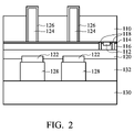
- FIG. 2 illustrates a thinning process performed on a backside of the semiconductor substrate 110 to expose the through-silicon vias 124 /liners 126 in accordance with an embodiment of the present invention.
- the thinning process may be performed using a mechanical grinding process, a chemical mechanical polishing (CMP) process, an etching process, and/or a combination thereof.
- CMP chemical mechanical polishing
- a planarizing process such as grinding or a CMP, may be performed to initially expose the through-silicon vias 124 .
- a wet or dry etching process having a high etch-rate selectivity between the material of the liners 126 and the material of the semiconductor substrate 110 may be performed to recess the semiconductor substrate 110 , thereby leaving the through-silicon vias 124 and the liners 126 protruding from the underside of the semiconductor substrate 110 as illustrated in FIG. 2 .
- the semiconductor substrate 110 may be recessed by, for example, performing a dry etch process using HBr/O 2 , HBr/Cl 2 /O 2 , SF 6 /CL 2 , SF 6 plasma, or the like.
- the through-silicon vias 124 and the liners 126 are exposed in the range of about sub- ⁇ m to about a few ⁇ ms.
- FIG. 3 illustrates a first isolation film 310 formed over the backside of the semiconductor substrate 110 (or a native oxide that may be formed on the surface of the semiconductor substrate 110 ) in accordance with an embodiment of the present invention.
- the first isolation film 310 is a dielectric material, such as SiN, an oxide, SiC, SiON, a polymer, or the like, and may be formed by, for example, spin-coating, printing, a CVD process, or the like.
- the first isolation film 310 is formed using a low-temperature process, e.g., using temperatures less than 250° C. by a PECVD process, preventing the bonding adhesive from degrading to ensure the mechanical strength throughout the integration process.
- the first isolation film 310 is preferably formed having a thickness sufficient to cover the exposed through-silicon vias 124 .
- the first isolation film 310 it may be desirable to perform a planarization process.
- some methods of deposition such as spin-coating, create a planar surface
- other methods such as a CVD process, form a conformal layer
- it may be desirable to perform a planarization process such as a grinding or CMP process, to create a planar surface as illustrated in FIG. 3 .
- FIG. 4 illustrates a second exposure of the through-silicon vias 124 in accordance with an embodiment of the present invention.
- the thinning process may be performed using a mechanical grinding process, a CMP process, an etching process, and/or a combination thereof.
- a planarizing process such as grinding or a CMP, may be performed to initially expose the through-silicon vias 124 .
- a wet or dry etching process having a high etch-rate selectivity between the material of the through-silicon vias 124 and the liners 126 and the material of the first isolation film 310 may be performed to recess the first isolation film 310 , thereby leaving the through-silicon vias 124 protruding from the underside of the isolation film 310 as illustrated in FIG. 4 .
- the through-silicon vias 124 are formed of copper and the first isolation film 310 is formed of silicon dioxide
- the first isolation film 310 may be recessed by performing a wet etch using hydrofluoric acid or a dry etching process. Other processes and materials may be used.
- the through-silicon vias 124 are exposed in the range of about sub- ⁇ m to about a few ⁇ ms.
- FIG. 4 also illustrates removing the liners 126 from the exposed portions of the through-silicon vias 124 along with the recess step of the first isolation film 310 .
- a conformal seed layer 510 is deposited over the surface of the isolation film 310 and the exposed portions of the through-silicon vias 124 .
- the seed layer 510 is a thin layer of a conductive material that aids in the formation of a thicker layer during subsequent processing steps.
- the seed layer 510 may be formed by depositing a thin conductive layer, such as a thin layer of Cu, Ti, Ta, TiN, TaN, or the like, using CVD or PVD techniques. For example, a layer of Ti is deposited by a PVD process to form a barrier film and a layer of Cu is deposited by a PVD process to form a seed layer.
- FIG. 6 illustrates a first patterned mask 610 formed over the seed layer 510 in accordance with an embodiment of the present invention.
- the first patterned mask 610 will act as a mold for forming conductive pads and redistribution lines in subsequent processing steps.
- the first patterned mask 610 may be a patterned photoresist mask, hard mask, or the like.
- a photoresist material is deposited to a thickness of about sub- ⁇ ms to about several ⁇ ms and patterned to form openings 612 over the through-silicon vias 124 .
- the embodiment illustrated in FIG. 6 preferably utilizes a re-entrant profile such that the openings 612 are wider along the bottom of the openings along the seed layer 510 than the top portion of the openings 612 .
- the re-entrant profile may be created by any suitable technique, such as the use of multiple photoresist layers with different patterning properties and one or more exposures, diffusion techniques, an image reversal process, or the like.
- the first patterned mask 610 may utilize a taper profile such that the openings 612 are narrower along a bottom of the opening along the seed layer 510 than the top portion of the openings 612 .
- conductive elements 710 are formed in the openings 612 (see FIG. 6 ) as illustrated in FIG. 7 .
- the conductive elements 710 are preferably metal, such as copper, tungsten, or other conductive metal, and may be formed, for example, by electroplating, electroless plating, or the like.
- an electroplating process is used wherein the wafer is submerged or immersed in the electroplating solution.
- the wafer surface is electrically connected to the negative side of an external DC power supply such that the wafer functions as the cathode in the electroplating process.
- a solid conductive anode, such as a copper anode is also immersed in the solution and is attached to the positive side of the power supply.
- the atoms from the anode are dissolved into the solution, from which the cathode, e.g., the wafer, acquires, thereby plating the exposed conductive areas of the wafer, e.g., exposed portions of the seed layer 510 within the openings 612 .
- the conductive elements 710 may be contact pads and/or redistribution lines. As illustrated in FIG. 14 , which is a plan view of the embodiments illustrated in FIGS. 1-13 , the conductive element 710 on the left side of FIG. 7 is a contact pad, whereas the conductive element 710 on the right side of FIG. 7 is a contact pad and a redistribution line.
- the redistribution line allows an electrical connection to another device, such as a die, wafer, packaging substrate, or the like, at a location other than the location of the TSV. This allows for greater flexibility and a higher degree of independence regarding the placement of the TSVs, the electrical circuitry on the substrate, and the pin-out locations.
- FIG. 8 illustrates the removal of the first patterned mask 610 (see FIGS. 6 and 7 ) in accordance with an embodiment of the present invention.
- a plasma ashing or wet strip process may be used to remove the first patterned mask 610 .
- One preferred plasma ashing process uses an O 2 flow rate of about 1000 sccm to about 2000 sccm at a pressure of about 300 mTorr to about 600 mTorr and at power of about 500 Watts to about 2000 Watts and at a temperature of about 80° C. to about 200° C., for example.
- the plasma ashing process may be followed by a wet dip in a sulfuric acid (H 2 SO 4 ) solution to clean the wafer and remove remaining photoresist material.
- H 2 SO 4 sulfuric acid
- FIG. 9 illustrates removal of the exposed portions of the seed layer 510 .
- Exposed portions of the seed layer 510 may be removed by, for example, a wet etching process.
- FIG. 10 illustrates formation of a second isolation film 1010 in accordance with an embodiment of the present invention.
- the second isolation film 1010 may be formed using similar processes and materials as those used to form the first isolation film 310 . It is preferable, however, that the material used to form the second isolation film 1010 have a high etch rate selectivity with the material used to form the first isolation film 310 . In this manner, the first isolation film 310 (and the conductive elements 710 ) may be used as an etch stop when patterning the second isolation film 1010 in a subsequent processing step.
- the second isolation film 1010 preferably has a thickness of about 2000 ⁇ to about 8000 ⁇ . As will be discussed below, the second isolation film 1010 will be patterned to isolate portions of the redistribution line while leaving contact pad locations exposed.
- FIG. 11 illustrates forming a second patterned mask 1110 in accordance with an embodiment of the present invention.
- the second patterned mask 1110 may be formed using similar materials, e.g., photoresist or hard mask materials, and similar processes as the first patterned mask 610 . It should be noted, however, that the first patterned mask 610 preferably utilized techniques that created a re-entrant pattern, but the second patterned mask 1110 has a vertical pattern. As such, for example, any suitable photolithography technique may be used to create the second patterned mask 1110 .
- FIG. 12 illustrates patterning the second isolation film 1010 and removing the second patterned mask 1110 in accordance with an embodiment of the present invention.
- the second isolation film 1010 may be patterned using a dry etching process, wherein the process has a high etch rate selectivity between the silicon nitride of the second isolation film 1010 and the silicon dioxide of the first isolation film 310 .
- the second patterned mask 1110 may be removed as illustrated in FIG. 12 .
- the second patterned mask 1110 may be removed by, for example, a plasma ashing process or a wet strip process as discussed above with reference to FIG. 7 .
- a cleaning step such as a wet dip in sulfuric acid, may be performed after removing the second patterned mask 1110 to remove any contaminants from the surface.
- FIG. 13 illustrates forming a contact barrier layer 1310 in accordance with an embodiment of the present invention.
- the contact barrier layer 1310 represents the conductive contact points where external devices, e.g., another die, wafer, circuit board, package board, or the like, make an electrical connection.
- the contact barrier layer 1310 is in electrical contact with the TSVs 124 , which in turn are in electrical contact with electrical circuitry formed on the substrate, such as electrical circuitry 112 , or to another external device, such as another die, wafer, circuit board, package board, or the like.
- the contact barrier layer 1310 is formed of a metal or metal alloy, such as Ni, AuSu, Au, or the like, using electroless plating techniques. Other methods and techniques, however, may be used.
- the material for the contact barrier layer 1310 should be selected to enhance the adhesion properties between the conductive elements 710 and the contact element on the external device. It should be noted that the conductive elements 710 and the contact barrier layer 1310 together form contact pads on which other devices, such as dies, wafers, substrates, or the like, may be connected.
- FIG. 14 is a plan view of an arrangement of the contact pads 1410 and the redistribution lines 1412 in accordance with an embodiment of the present invention.
- FIGS. 1-13 are cross section views taken along the A-A line.
- the second isolation film 1010 acts as a passivation layer and covers the backside of the substrate, except for the exposed contact pads 1410 (e.g., the contact barrier layer 1310 and the underlying conductive elements 710 ).
- the second isolation film 1010 is formed over the redistribution lines, which are shown by the dotted lines.
- the embodiments discussed above allow the simultaneous formation of the contact pads and the redistribution line.
- the use of a redistribution layer allows the same design to be utilized with different pin-outs and technologies.
- the conductive bumps with tapered sidewalls also provide a larger bonding interface for wafer and/or die stacking processes.
- FIGS. 15-17 illustrate bonding the structure discussed above with reference to FIGS. 1-14 to another structure in accordance with an embodiment of the present invention.
- a substrate 1510 is shown having top metal contacts 1512 and connection elements 1514 .
- the connection elements 1514 may be, for example, solder balls.
- the substrate 1510 may be attached to the semiconductor substrate 110 by aligning the connection elements 1514 with the contact pads 1410 and applying pressure and/or heat to cause the connection elements 1514 to adhere and form an electrical connection to the contact barrier layer 1310 as illustrated in FIG. 16 . Due to the taper-like shape of the contact barrier layer 1310 and the conductive elements 710 , a larger wetting surface for the bonding interface is provided, thereby creating a better electrical connection as well as providing additional structural support.
- the temporary carrier substrate 130 may be removed, allowing the conductive bumps 128 on the circuit-side of the semiconductor substrate 110 to be bonded to another die, wafer, substrate, or board. Thereafter, other back-end-of-line processing techniques suitable for the particular application may be performed. For example, a filler material may be injected between stacked dies, an encapsulant may be formed, a singulation process may be performed to singulate individual stacked-die packages, and the like, may be performed. It should be noted, however, that embodiments of the present invention may be used in many different situations. For example, embodiments of the present invention may be used in a die-to-die bonding configuration, a die-to-wafer bonding configuration, or a wafer-to-wafer bonding configuration.
Abstract
Description
Claims (12)
Priority Applications (4)
| Application Number | Priority Date | Filing Date | Title |
|---|---|---|---|
| US12/331,900 US8513119B2 (en) | 2008-12-10 | 2008-12-10 | Method of forming bump structure having tapered sidewalls for stacked dies |
| TW098115087A TWI416692B (en) | 2008-12-10 | 2009-05-07 | Semiconductor device and method for forming the same |
| CN2009101410820A CN101752336B (en) | 2008-12-10 | 2009-05-20 | Semiconductor device and manufacturing method thereof |
| US13/943,543 US9312225B2 (en) | 2008-12-10 | 2013-07-16 | Bump structure for stacked dies |
Applications Claiming Priority (1)
| Application Number | Priority Date | Filing Date | Title |
|---|---|---|---|
| US12/331,900 US8513119B2 (en) | 2008-12-10 | 2008-12-10 | Method of forming bump structure having tapered sidewalls for stacked dies |
Related Child Applications (1)
| Application Number | Title | Priority Date | Filing Date |
|---|---|---|---|
| US13/943,543 Division US9312225B2 (en) | 2008-12-10 | 2013-07-16 | Bump structure for stacked dies |
Publications (2)
| Publication Number | Publication Date |
|---|---|
| US20100140805A1 US20100140805A1 (en) | 2010-06-10 |
| US8513119B2 true US8513119B2 (en) | 2013-08-20 |
Family
ID=42230179
Family Applications (2)
| Application Number | Title | Priority Date | Filing Date |
|---|---|---|---|
| US12/331,900 Active 2029-01-13 US8513119B2 (en) | 2008-12-10 | 2008-12-10 | Method of forming bump structure having tapered sidewalls for stacked dies |
| US13/943,543 Active US9312225B2 (en) | 2008-12-10 | 2013-07-16 | Bump structure for stacked dies |
Family Applications After (1)
| Application Number | Title | Priority Date | Filing Date |
|---|---|---|---|
| US13/943,543 Active US9312225B2 (en) | 2008-12-10 | 2013-07-16 | Bump structure for stacked dies |
Country Status (3)
| Country | Link |
|---|---|
| US (2) | US8513119B2 (en) |
| CN (1) | CN101752336B (en) |
| TW (1) | TWI416692B (en) |
Cited By (16)
| Publication number | Priority date | Publication date | Assignee | Title |
|---|---|---|---|---|
| US20110068466A1 (en) * | 2009-09-22 | 2011-03-24 | Taiwan Semiconductor Manufacturing Company, Ltd. | Wafer Backside Interconnect Structure Connected to TSVs |
| US20130026606A1 (en) * | 2011-07-29 | 2013-01-31 | International Business Machines Corporation | Tsv pillar as an interconnecting structure |
| US8841773B2 (en) | 2010-03-30 | 2014-09-23 | Taiwan Semiconductor Manufacturing Company, Ltd. | Multi-layer interconnect structure for stacked dies |
| US8900994B2 (en) | 2011-06-09 | 2014-12-02 | Taiwan Semiconductor Manufacturing Company, Ltd. | Method for producing a protective structure |
| US9059027B2 (en) * | 2013-09-12 | 2015-06-16 | Kabushiki Kaisha Toshiba | Semiconductor device |
| US20160099201A1 (en) * | 2014-10-06 | 2016-04-07 | Ju-Il Choi | Integrated circuit devices having through-silicon vias and methods of manufacturing such devices |
| US9312225B2 (en) | 2008-12-10 | 2016-04-12 | Taiwan Semiconductor Manufacturing Company, Ltd. | Bump structure for stacked dies |
| US9728490B2 (en) | 2015-08-24 | 2017-08-08 | Samsung Electronics Co., Ltd. | Semiconductor devices and methods of manufacturing the same |
| US9806004B2 (en) | 2014-12-01 | 2017-10-31 | Samsung Electronics Co., Ltd. | Semiconductor devices having a TSV, a front-side bumping pad, and a back-side bumping pad |
| US10163756B2 (en) | 2009-01-05 | 2018-12-25 | Taiwan Semiconductor Manufacturing Company, Ltd. | Isolation structure for stacked dies |
| US10658287B2 (en) * | 2018-05-30 | 2020-05-19 | Taiwan Semiconductor Manufacturing Co., Ltd. | Semiconductor device having a tapered protruding pillar portion |
| US11049827B2 (en) | 2019-08-09 | 2021-06-29 | Samsung Electronics Co., Ltd. | Semiconductor devices including a thick metal layer and a bump |
| US20220028699A1 (en) * | 2020-07-21 | 2022-01-27 | Infineon Technologies Austria Ag | Chip-substrate composite semiconductor device |
| TWI755485B (en) * | 2017-02-20 | 2022-02-21 | 新加坡商西拉娜亞洲私人有限公司 | Integrated circuit package apparatus and integrated circuit packaging method for minimizing crosstalk |
| US11335627B2 (en) | 2017-02-20 | 2022-05-17 | Silanna Asia Pte Ltd | Connection arrangements for integrated lateral diffusion field effect transistors having a backside contact |
| US20220157694A1 (en) * | 2018-07-31 | 2022-05-19 | Intel Corporation | Micro through-silicon via for transistor density scaling |
Families Citing this family (51)
| Publication number | Priority date | Publication date | Assignee | Title |
|---|---|---|---|---|
| US8399354B2 (en) * | 2009-01-13 | 2013-03-19 | Taiwan Semiconductor Manufacturing Company, Ltd. | Through-silicon via with low-K dielectric liner |
| TWI414044B (en) * | 2009-12-29 | 2013-11-01 | Advanced Semiconductor Eng | Semiconductor process, semiconductor element and package having semiconductor element |
| US8896136B2 (en) * | 2010-06-30 | 2014-11-25 | Taiwan Semiconductor Manufacturing Company, Ltd. | Alignment mark and method of formation |
| US8227924B2 (en) * | 2010-07-13 | 2012-07-24 | Taiwan Semiconductor Manufacturing Company, Ltd. | Substrate stand-offs for semiconductor devices |
| US8754516B2 (en) | 2010-08-26 | 2014-06-17 | Intel Corporation | Bumpless build-up layer package with pre-stacked microelectronic devices |
| US8466553B2 (en) | 2010-10-12 | 2013-06-18 | Advanced Semiconductor Engineering, Inc. | Semiconductor device and semiconductor package having the same |
| US8105875B1 (en) | 2010-10-14 | 2012-01-31 | Taiwan Semiconductor Manufacturing Company, Ltd. | Approach for bonding dies onto interposers |
| US8936966B2 (en) | 2012-02-08 | 2015-01-20 | Taiwan Semiconductor Manufacturing Company, Ltd. | Packaging methods for semiconductor devices |
| US9064879B2 (en) | 2010-10-14 | 2015-06-23 | Taiwan Semiconductor Manufacturing Company, Ltd. | Packaging methods and structures using a die attach film |
| US8455984B2 (en) * | 2010-11-15 | 2013-06-04 | Nanya Technology Corp. | Integrated circuit structure and method of forming the same |
| KR101697573B1 (en) * | 2010-11-29 | 2017-01-19 | 삼성전자 주식회사 | Semiconductor device, fabricating method thereof, and semiconductor package comprising the semiconductor device |
| KR101215648B1 (en) * | 2011-02-11 | 2012-12-26 | 에스케이하이닉스 주식회사 | Semiconductor chip and method for manufacturing the same |
| US20120256190A1 (en) * | 2011-04-11 | 2012-10-11 | International Rectifier Corporation | Stacked Composite Device Including a Group III-V Transistor and a Group IV Diode |
| US9343440B2 (en) | 2011-04-11 | 2016-05-17 | Infineon Technologies Americas Corp. | Stacked composite device including a group III-V transistor and a group IV vertical transistor |
| US8987833B2 (en) | 2011-04-11 | 2015-03-24 | International Rectifier Corporation | Stacked composite device including a group III-V transistor and a group IV lateral transistor |
| US8304916B1 (en) * | 2011-07-06 | 2012-11-06 | Northrop Grumman Systems Corporation | Half-through vias for suppression of substrate modes |
| KR101918609B1 (en) | 2012-01-11 | 2018-11-14 | 삼성전자 주식회사 | Integrated circuit device |
| US8519516B1 (en) * | 2012-03-12 | 2013-08-27 | Micron Technology, Inc. | Semiconductor constructions |
| US9362267B2 (en) | 2012-03-15 | 2016-06-07 | Infineon Technologies Americas Corp. | Group III-V and group IV composite switch |
| CN103367241B (en) * | 2012-04-09 | 2015-05-27 | 南亚科技股份有限公司 | Through silicon via exposing method |
| US9030010B2 (en) | 2012-09-20 | 2015-05-12 | Taiwan Semiconductor Manufacturing Company, Ltd. | Packaging devices and methods |
| JP5772926B2 (en) * | 2013-01-07 | 2015-09-02 | 株式会社デンソー | Semiconductor device |
| US8912091B2 (en) | 2013-01-10 | 2014-12-16 | International Business Machines Corporation | Backside metal ground plane with improved metal adhesion and design structures |
| US9059111B2 (en) * | 2013-04-11 | 2015-06-16 | International Business Machines Corporation | Reliable back-side-metal structure |
| US20140327132A1 (en) * | 2013-05-03 | 2014-11-06 | National Center For Advanced Packaging (Ncap China) | TSV Backside Reveal Structure and Exposing Process |
| CN104183571B (en) * | 2013-05-27 | 2018-01-23 | 联华电子股份有限公司 | Straight-through silicon wafer perforation and its manufacture craft |
| KR20150048388A (en) * | 2013-10-28 | 2015-05-07 | 삼성전자주식회사 | Semiconductor device and method of manufacturing the same |
| CN103730351A (en) * | 2014-01-07 | 2014-04-16 | 上海华虹宏力半导体制造有限公司 | Post-etching ashing method and forming method of magnetic sensor |
| US10157823B2 (en) * | 2014-10-31 | 2018-12-18 | Qualcomm Incorporated | High density fan out package structure |
| TWI582918B (en) * | 2014-11-12 | 2017-05-11 | 精材科技股份有限公司 | Chip package and manufacturing method thereof |
| TWI581325B (en) * | 2014-11-12 | 2017-05-01 | 精材科技股份有限公司 | Chip package and manufacturing method thereof |
| US9941190B2 (en) * | 2015-04-03 | 2018-04-10 | Micron Technology, Inc. | Semiconductor device having through-silicon-via and methods of forming the same |
| JP2016213247A (en) * | 2015-04-30 | 2016-12-15 | 国立研究開発法人産業技術総合研究所 | Through electrode, manufacturing method of the same, semiconductor device, and manufacturing method of the same |
| US9754909B2 (en) | 2015-05-26 | 2017-09-05 | Monolithic Power Systems, Inc. | Copper structures with intermetallic coating for integrated circuit chips |
| ES2742705T3 (en) * | 2015-07-30 | 2020-02-17 | Heidenhain Gmbh Dr Johannes | Position measuring device |
| TWI605544B (en) * | 2015-11-25 | 2017-11-11 | 矽品精密工業股份有限公司 | Substrate structure and method of fabrication |
| US10147682B2 (en) * | 2015-11-30 | 2018-12-04 | Taiwan Semiconductor Manufacturing Co., Ltd. | Structure for stacked logic performance improvement |
| CN105550432A (en) * | 2015-12-11 | 2016-05-04 | 格科微电子(上海)有限公司 | Three-dimensional integrated circuit chip and power network layout method thereof |
| US10607885B2 (en) * | 2016-03-30 | 2020-03-31 | Intel Corporation | Shell structure for insulation of a through-substrate interconnect |
| US10366953B2 (en) * | 2016-12-05 | 2019-07-30 | Taiwan Semiconductor Manufacturing Co., Ltd. | Redistribution layer structures for integrated circuit package |
| DE102017123449B4 (en) * | 2017-04-10 | 2023-12-28 | Taiwan Semiconductor Manufacturing Co. Ltd. | Housing with Si-substrate-free intermediate piece and training process |
| KR20180136148A (en) * | 2017-06-14 | 2018-12-24 | 에스케이하이닉스 주식회사 | Semiconductor device having bump |
| CN109285825B (en) * | 2017-07-21 | 2021-02-05 | 联华电子股份有限公司 | Chip stacking structure and manufacturing method of tube core stacking structure |
| CN110752162B (en) * | 2018-07-23 | 2021-05-07 | 西安电子科技大学 | Pre-distortion integrated circuit based on X-band gallium nitride and manufacturing method |
| US11764343B2 (en) | 2019-05-31 | 2023-09-19 | Boe Technology Group Co., Ltd. | Display backboard and manufacturing method thereof and display device |
| EP3979343A4 (en) | 2019-05-31 | 2023-05-24 | Boe Technology Group Co., Ltd. | Display back plate and manufacturing method, display panel and manufacturing method, and display device |
| JP7464540B2 (en) | 2019-08-16 | 2024-04-09 | 京東方科技集團股▲ふん▼有限公司 | Display backplane and its manufacturing method, display device |
| US11264368B2 (en) | 2019-08-28 | 2022-03-01 | Taiwan Semiconductor Manufacturing Company, Ltd. | Mask transfer method (and related apparatus) for a bumping process |
| KR102445598B1 (en) * | 2019-08-28 | 2022-09-20 | 타이완 세미콘덕터 매뉴팩쳐링 컴퍼니 리미티드 | An integrated circuit (ic) and a method for forming the same |
| CN111554647B (en) * | 2020-05-19 | 2022-04-19 | 上海先方半导体有限公司 | Wafer-level chip structure, multi-chip stacking interconnection structure and preparation method |
| CN116314016B (en) * | 2023-04-26 | 2023-10-03 | 北京大学 | Submicron-sized through silicon via structure, preparation method thereof and electronic equipment |
Citations (71)
| Publication number | Priority date | Publication date | Assignee | Title |
|---|---|---|---|---|
| US5391917A (en) | 1993-05-10 | 1995-02-21 | International Business Machines Corporation | Multiprocessor module packaging |
| US5426072A (en) | 1993-01-21 | 1995-06-20 | Hughes Aircraft Company | Process of manufacturing a three dimensional integrated circuit from stacked SOI wafers using a temporary silicon substrate |
| US5510298A (en) | 1991-09-12 | 1996-04-23 | Texas Instruments Incorporated | Method of interconnect in an integrated circuit |
| US5646067A (en) | 1995-06-05 | 1997-07-08 | Harris Corporation | Method of bonding wafers having vias including conductive material |
| US5767001A (en) | 1993-05-05 | 1998-06-16 | Siemens Aktiengesellschaft | Process for producing semiconductor components between which contact is made vertically |
| US5998292A (en) | 1997-11-12 | 1999-12-07 | International Business Machines Corporation | Method for making three dimensional circuit integration |
| US6034436A (en) | 1996-11-28 | 2000-03-07 | Nec Corporation | Semiconductor device having an improved through-hole structure |
| US6184060B1 (en) | 1996-10-29 | 2001-02-06 | Trusi Technologies Llc | Integrated circuits and methods for their fabrication |
| US6322903B1 (en) | 1999-12-06 | 2001-11-27 | Tru-Si Technologies, Inc. | Package of integrated circuits and vertical integration |
| US20020084513A1 (en) | 1996-10-29 | 2002-07-04 | Oleg Siniaguine | Integrated circuits and methods for their fabrication |
| US6417087B1 (en) | 1999-12-16 | 2002-07-09 | Agere Systems Guardian Corp. | Process for forming a dual damascene bond pad structure over active circuitry |
| US20020113321A1 (en) | 2001-02-22 | 2002-08-22 | Oleg Siniaguine | Devices having substrates with opening passing through the substrates and conductors in the openings, and methods of manufacture |
| US6448168B1 (en) | 1997-09-30 | 2002-09-10 | Intel Corporation | Method for distributing a clock on the silicon backside of an integrated circuit |
| US6451684B1 (en) * | 1998-07-21 | 2002-09-17 | Samsung Electronics Co., Ltd. | Semiconductor device having a conductive layer side surface slope which is at least 90° and method for manufacturing the same |
| US6465892B1 (en) | 1999-04-13 | 2002-10-15 | Oki Electric Industry Co., Ltd. | Interconnect structure for stacked semiconductor device |
| US20020182855A1 (en) | 2001-06-01 | 2002-12-05 | Agarwala Birendra N. | Dual damascene multi-level metallization |
| US6498381B2 (en) | 2001-02-22 | 2002-12-24 | Tru-Si Technologies, Inc. | Semiconductor structures having multiple conductive layers in an opening, and methods for fabricating same |
| US6538333B2 (en) | 2000-06-16 | 2003-03-25 | Chartered Semiconductor Manufacturing Ltd. | Three dimensional IC package module |
| US6599778B2 (en) | 2001-12-19 | 2003-07-29 | International Business Machines Corporation | Chip and wafer integration process using vertical connections |
| US20030148600A1 (en) | 1999-07-01 | 2003-08-07 | Hitachi, Ltd. | Method of forming conductive layers in the trenches or through holes made in an insulating film on a semiconductor substrate |
| US20040048459A1 (en) | 2002-04-11 | 2004-03-11 | Robert Patti | Interlocking conductor method for bonding wafers to produce stacked integrated circuits |
| US6800930B2 (en) | 2002-07-31 | 2004-10-05 | Micron Technology, Inc. | Semiconductor dice having back side redistribution layer accessed using through-silicon vias, and assemblies |
| US20040245623A1 (en) | 2003-03-28 | 2004-12-09 | Kazumi Hara | Semiconductor device, circuit substrate and electronic instrument |
| US6841883B1 (en) | 2003-03-31 | 2005-01-11 | Micron Technology, Inc. | Multi-dice chip scale semiconductor components and wafer level methods of fabrication |
| US6873054B2 (en) * | 2002-04-24 | 2005-03-29 | Seiko Epson Corporation | Semiconductor device and a method of manufacturing the same, a circuit board and an electronic apparatus |
| US6897125B2 (en) | 2003-09-17 | 2005-05-24 | Intel Corporation | Methods of forming backside connections on a wafer stack |
| US6908856B2 (en) | 2003-04-03 | 2005-06-21 | Interuniversitair Microelektronica Centrum (Imec) | Method for producing electrical through hole interconnects and devices made thereof |
| US6924551B2 (en) | 2003-05-28 | 2005-08-02 | Intel Corporation | Through silicon via, folded flex microelectronic package |
| US20050221601A1 (en) | 2004-03-31 | 2005-10-06 | Nec Electronics Corporation | Semiconductor device and method for manufacturing the same |
| US20050233581A1 (en) | 2004-03-31 | 2005-10-20 | Nec Electronics Corporation | Method for manufacturing semiconductor device |
| US6962872B2 (en) | 2002-12-09 | 2005-11-08 | International Business Machines Corporation | High density chip carrier with integrated passive devices |
| US7049170B2 (en) | 2003-12-17 | 2006-05-23 | Tru-Si Technologies, Inc. | Integrated circuits and packaging substrates with cavities, and attachment methods including insertion of protruding contact pads into cavities |
| US7060601B2 (en) | 2003-12-17 | 2006-06-13 | Tru-Si Technologies, Inc. | Packaging substrates for integrated circuits and soldering methods |
| US7071546B2 (en) | 2002-01-16 | 2006-07-04 | Alfred E. Mann Foundation For Scientific Research | Space-saving packaging of electronic circuits |
| US7111149B2 (en) | 2003-07-07 | 2006-09-19 | Intel Corporation | Method and apparatus for generating a device ID for stacked devices |
| US7122912B2 (en) | 2004-01-28 | 2006-10-17 | Nec Electronics Corporation | Chip and multi-chip semiconductor device using thereof and method for manufacturing same |
| US20060273465A1 (en) | 2005-06-06 | 2006-12-07 | Sharp Kabushiki Kaisha | Semiconductor device and manufacturing method therefor |
| US20060289968A1 (en) | 2005-06-28 | 2006-12-28 | Micron Technology, Inc. | Conductive interconnect structures and formation methods using supercritical fluids |
| US7157787B2 (en) | 2002-02-20 | 2007-01-02 | Intel Corporation | Process of vertically stacking multiple wafers supporting different active integrated circuit (IC) devices |
| US20070032061A1 (en) | 2005-08-05 | 2007-02-08 | Farnworth Warren M | Methods of forming through-wafer interconnects and structures resulting therefrom |
| US20070049016A1 (en) | 2005-09-01 | 2007-03-01 | Micron Technology, Inc. | Microfeature workpieces and methods for forming interconnects in microfeature workpieces |
| US7193308B2 (en) | 2003-09-26 | 2007-03-20 | Seiko Epson Corporation | Intermediate chip module, semiconductor device, circuit board, and electronic device |
| US7262495B2 (en) | 2004-10-07 | 2007-08-28 | Hewlett-Packard Development Company, L.P. | 3D interconnect with protruding contacts |
| US7297574B2 (en) | 2005-06-17 | 2007-11-20 | Infineon Technologies Ag | Multi-chip device and method for producing a multi-chip device |
| US7300857B2 (en) | 2004-09-02 | 2007-11-27 | Micron Technology, Inc. | Through-wafer interconnects for photoimager and memory wafers |
| US7335972B2 (en) | 2003-11-13 | 2008-02-26 | Sandia Corporation | Heterogeneously integrated microsystem-on-a-chip |
| US20080054444A1 (en) | 2006-08-31 | 2008-03-06 | Micron Technology, Inc. | Microfeature workpieces having interconnects and conductive backplanes, and associated systems and methods |
| US20080136023A1 (en) | 2006-12-06 | 2008-06-12 | Sony Corporation | Method for manufacturing semiconductor device and semiconductor device |
| US20080211106A1 (en) | 2007-03-01 | 2008-09-04 | Taiwan Semiconductor Manufacturing Co., Ltd. | Via/contact and damascene structures and manufacturing methods thereof |
| JP2009004730A (en) | 2007-06-22 | 2009-01-08 | Ind Technol Res Inst | Self matching wafer or chip structure, self matching laminate structure, and manufacturing method thereof |
| US20090014843A1 (en) | 2007-06-06 | 2009-01-15 | Kawashita Michihiro | Manufacturing process and structure of through silicon via |
| US7514775B2 (en) | 2006-10-09 | 2009-04-07 | Taiwan Semiconductor Manufacturing Co., Ltd. | Stacked structures and methods of fabricating stacked structures |
| US20090152602A1 (en) | 2007-12-17 | 2009-06-18 | Kazutaka Akiyama | Semiconductor device and method for manufacturing the same |
| US20090269905A1 (en) | 2007-05-16 | 2009-10-29 | Chen-Shien Chen | Tapered Through-Silicon Via Structure |
| US20090283898A1 (en) * | 2008-05-15 | 2009-11-19 | Janzen Jeffery W | Disabling electrical connections using pass-through 3d interconnects and associated systems and methods |
| US20090315184A1 (en) | 2008-05-26 | 2009-12-24 | Oki Semiconductor Co., Ltd. | Semiconductor Device |
| US20100013060A1 (en) | 2008-06-22 | 2010-01-21 | Taiwan Semiconductor Manufacturing Company, Ltd. | Method of forming a conductive trench in a silicon wafer and silicon wafer comprising such trench |
| US20100038800A1 (en) | 2008-08-18 | 2010-02-18 | Samsung Electronics Co., Ltd. | Through-silicon via structures including conductive protective layers and methods of forming the same |
| US20100127394A1 (en) | 2008-11-25 | 2010-05-27 | Freescale Semiconductor, Inc. | Through substrate vias for back-side interconnections on very thin semiconductor wafers |
| US20100171226A1 (en) | 2008-12-29 | 2010-07-08 | Texas Instruments, Inc. | Ic having tsv arrays with reduced tsv induced stress |
| US20100171197A1 (en) | 2009-01-05 | 2010-07-08 | Hung-Pin Chang | Isolation Structure for Stacked Dies |
| US7772081B2 (en) * | 2008-09-17 | 2010-08-10 | Stats Chippac, Ltd. | Semiconductor device and method of forming high-frequency circuit structure and method thereof |
| US7772116B2 (en) * | 2005-09-01 | 2010-08-10 | Micron Technology, Inc. | Methods of forming blind wafer interconnects |
| US20100330798A1 (en) | 2009-06-26 | 2010-12-30 | Taiwan Semiconductor Manufacturing Company, Ltd. | Formation of TSV Backside Interconnects by Modifying Carrier Wafers |
| US20110049706A1 (en) | 2009-09-03 | 2011-03-03 | Taiwan Semiconductor Manufacturing Company, Ltd. | Front Side Copper Post Joint Structure for Temporary Bond in TSV Application |
| US20110068466A1 (en) | 2009-09-22 | 2011-03-24 | Taiwan Semiconductor Manufacturing Company, Ltd. | Wafer Backside Interconnect Structure Connected to TSVs |
| US20110186990A1 (en) | 2010-01-29 | 2011-08-04 | Texas Instruments Incorporated | Protruding tsv tips for enhanced heat dissipation for ic devices |
| US20110233785A1 (en) | 2010-03-24 | 2011-09-29 | International Business Machines Corporation | Backside dummy plugs for 3d integration |
| US20110241217A1 (en) | 2010-03-30 | 2011-10-06 | Taiwan Semiconductor Manufacturing Company, Ltd. | Multi-Layer Interconnect Structure for Stacked Dies |
| US8174124B2 (en) | 2010-04-08 | 2012-05-08 | Taiwan Semiconductor Manufacturing Co., Ltd. | Dummy pattern in wafer backside routing |
| US8264077B2 (en) | 2008-12-29 | 2012-09-11 | Taiwan Semiconductor Manufacturing Company, Ltd. | Backside metal of redistribution line with silicide layer on through-silicon via of semiconductor chips |
Family Cites Families (46)
| Publication number | Priority date | Publication date | Assignee | Title |
|---|---|---|---|---|
| US6706189B2 (en) | 1998-10-09 | 2004-03-16 | Zenon Environmental Inc. | Cyclic aeration system for submerged membrane modules |
| JP3626058B2 (en) | 2000-01-25 | 2005-03-02 | Necエレクトロニクス株式会社 | Manufacturing method of semiconductor device |
| JP2001291720A (en) | 2000-04-05 | 2001-10-19 | Hitachi Ltd | Semiconductor integrated circuit device and its manufacturing method |
| US7053465B2 (en) | 2000-11-28 | 2006-05-30 | Texas Instruments Incorporated | Semiconductor varactor with reduced parasitic resistance |
| US6696360B2 (en) | 2001-03-15 | 2004-02-24 | Micron Technology, Inc. | Barrier-metal-free copper damascene technology using atomic hydrogen enhanced reflow |
| US6645796B2 (en) * | 2001-11-21 | 2003-11-11 | International Business Machines Corporation | Method and semiconductor structure for implementing reach through buried interconnect for silicon-on-insulator (SOI) devices |
| US7354798B2 (en) | 2002-12-20 | 2008-04-08 | International Business Machines Corporation | Three-dimensional device fabrication method |
| JP4072677B2 (en) | 2003-01-15 | 2008-04-09 | セイコーエプソン株式会社 | Semiconductor chip, semiconductor wafer, semiconductor device and manufacturing method thereof, circuit board, and electronic equipment |
| TWI241000B (en) | 2003-01-21 | 2005-10-01 | Siliconware Precision Industries Co Ltd | Semiconductor package and fabricating method thereof |
| US6878616B1 (en) | 2003-11-21 | 2005-04-12 | International Business Machines Corporation | Low-k dielectric material system for IC application |
| JP4339152B2 (en) | 2004-03-08 | 2009-10-07 | 富士通マイクロエレクトロニクス株式会社 | Method for forming wiring structure |
| US7906363B2 (en) | 2004-08-20 | 2011-03-15 | Zycube Co., Ltd. | Method of fabricating semiconductor device having three-dimensional stacked structure |
| US7109068B2 (en) | 2004-08-31 | 2006-09-19 | Micron Technology, Inc. | Through-substrate interconnect fabrication methods |
| KR20060054689A (en) | 2004-11-16 | 2006-05-23 | 강준모 | Semiconductor device having backside input output terminal and method of manufacturing the same |
| KR20060054690A (en) | 2004-11-16 | 2006-05-23 | 강준모 | Semiconductor device having backside input output terminal and method of manufacturing the same |
| KR101052366B1 (en) | 2004-11-16 | 2011-07-28 | 강준모 | Semiconductor device having rear input / output terminal and manufacturing method thereof |
| TWI287273B (en) | 2006-01-25 | 2007-09-21 | Advanced Semiconductor Eng | Three dimensional package and method of making the same |
| US7544605B2 (en) | 2006-11-21 | 2009-06-09 | Freescale Semiconductor, Inc. | Method of making a contact on a backside of a die |
| US20080246152A1 (en) * | 2007-04-04 | 2008-10-09 | Taiwan Semiconductor Manufacturing Co., Ltd. | Semiconductor device with bonding pad |
| KR20080101635A (en) | 2007-05-18 | 2008-11-21 | 삼성전자주식회사 | Semiconductor packages, method of fabricating the same, and package modules and electronic product using the semiconductor package |
| TW200910557A (en) | 2007-06-20 | 2009-03-01 | Flipchip Int Llc | Under bump metallization structure having a seed layer for electroless nickel deposition |
| US20090057909A1 (en) | 2007-06-20 | 2009-03-05 | Flipchip International, Llc | Under bump metallization structure having a seed layer for electroless nickel deposition |
| US8193092B2 (en) | 2007-07-31 | 2012-06-05 | Micron Technology, Inc. | Semiconductor devices including a through-substrate conductive member with an exposed end and methods of manufacturing such semiconductor devices |
| KR101387701B1 (en) | 2007-08-01 | 2014-04-23 | 삼성전자주식회사 | Semiconductor packages and methods for manufacturing the same |
| JP2009055004A (en) | 2007-08-24 | 2009-03-12 | Honda Motor Co Ltd | Through-wiring structure |
| JP5358089B2 (en) | 2007-12-21 | 2013-12-04 | スパンション エルエルシー | Semiconductor device |
| US7804119B2 (en) | 2008-04-08 | 2010-09-28 | International Business Machines Corporation | Device structures with a hyper-abrupt P-N junction, methods of forming a hyper-abrupt P-N junction, and design structures for an integrated circuit |
| US7968460B2 (en) | 2008-06-19 | 2011-06-28 | Micron Technology, Inc. | Semiconductor with through-substrate interconnect |
| US7855455B2 (en) | 2008-09-26 | 2010-12-21 | International Business Machines Corporation | Lock and key through-via method for wafer level 3 D integration and structures produced |
| US7928534B2 (en) | 2008-10-09 | 2011-04-19 | Taiwan Semiconductor Manufacturing Company, Ltd. | Bond pad connection to redistribution lines having tapered profiles |
| US8513119B2 (en) | 2008-12-10 | 2013-08-20 | Taiwan Semiconductor Manufacturing Company, Ltd. | Method of forming bump structure having tapered sidewalls for stacked dies |
| US7999320B2 (en) | 2008-12-23 | 2011-08-16 | International Business Machines Corporation | SOI radio frequency switch with enhanced signal fidelity and electrical isolation |
| US7910473B2 (en) | 2008-12-31 | 2011-03-22 | Taiwan Semiconductor Manufacturing Company, Ltd. | Through-silicon via with air gap |
| US8399354B2 (en) | 2009-01-13 | 2013-03-19 | Taiwan Semiconductor Manufacturing Company, Ltd. | Through-silicon via with low-K dielectric liner |
| US9070679B2 (en) | 2009-11-24 | 2015-06-30 | Marvell World Trade Ltd. | Semiconductor package with a semiconductor die embedded within substrates |
| US8273616B2 (en) | 2010-02-19 | 2012-09-25 | Taiwan Semiconductor Manufacturing Company, Ltd. | Gated-varactors |
| US20110227216A1 (en) | 2010-03-16 | 2011-09-22 | Taiwan Semiconductor Manufacturing Company, Ltd. | Under-Bump Metallization Structure for Semiconductor Devices |
| US9293366B2 (en) | 2010-04-28 | 2016-03-22 | Taiwan Semiconductor Manufacturing Company, Ltd. | Through-substrate vias with improved connections |
| US8896136B2 (en) | 2010-06-30 | 2014-11-25 | Taiwan Semiconductor Manufacturing Company, Ltd. | Alignment mark and method of formation |
| US8796135B2 (en) | 2010-07-23 | 2014-08-05 | Tessera, Inc. | Microelectronic elements with rear contacts connected with via first or via middle structures |
| US8466553B2 (en) | 2010-10-12 | 2013-06-18 | Advanced Semiconductor Engineering, Inc. | Semiconductor device and semiconductor package having the same |
| US20120193778A1 (en) | 2011-01-27 | 2012-08-02 | Texas Instruments Incorporated | Integrated circuit having protruding bonding features with reinforcing dielectric supports |
| US8273604B2 (en) | 2011-02-22 | 2012-09-25 | STAT ChipPAC, Ltd. | Semiconductor device and method of forming WLCSP structure using protruded MLP |
| US8481425B2 (en) | 2011-05-16 | 2013-07-09 | United Microelectronics Corp. | Method for fabricating through-silicon via structure |
| US8791009B2 (en) | 2011-06-07 | 2014-07-29 | International Business Machines Corporation | Method of forming a through-silicon via utilizing a metal contact pad in a back-end-of-line wiring level to fill the through-silicon via |
| US8900994B2 (en) | 2011-06-09 | 2014-12-02 | Taiwan Semiconductor Manufacturing Company, Ltd. | Method for producing a protective structure |
-
2008
- 2008-12-10 US US12/331,900 patent/US8513119B2/en active Active
-
2009
- 2009-05-07 TW TW098115087A patent/TWI416692B/en active
- 2009-05-20 CN CN2009101410820A patent/CN101752336B/en active Active
-
2013
- 2013-07-16 US US13/943,543 patent/US9312225B2/en active Active
Patent Citations (90)
| Publication number | Priority date | Publication date | Assignee | Title |
|---|---|---|---|---|
| US5510298A (en) | 1991-09-12 | 1996-04-23 | Texas Instruments Incorporated | Method of interconnect in an integrated circuit |
| US5426072A (en) | 1993-01-21 | 1995-06-20 | Hughes Aircraft Company | Process of manufacturing a three dimensional integrated circuit from stacked SOI wafers using a temporary silicon substrate |
| US5767001A (en) | 1993-05-05 | 1998-06-16 | Siemens Aktiengesellschaft | Process for producing semiconductor components between which contact is made vertically |
| US5391917A (en) | 1993-05-10 | 1995-02-21 | International Business Machines Corporation | Multiprocessor module packaging |
| US5646067A (en) | 1995-06-05 | 1997-07-08 | Harris Corporation | Method of bonding wafers having vias including conductive material |
| US20020084513A1 (en) | 1996-10-29 | 2002-07-04 | Oleg Siniaguine | Integrated circuits and methods for their fabrication |
| US6882030B2 (en) | 1996-10-29 | 2005-04-19 | Tru-Si Technologies, Inc. | Integrated circuit structures with a conductor formed in a through hole in a semiconductor substrate and protruding from a surface of the substrate |
| US6184060B1 (en) | 1996-10-29 | 2001-02-06 | Trusi Technologies Llc | Integrated circuits and methods for their fabrication |
| US6639303B2 (en) | 1996-10-29 | 2003-10-28 | Tru-Si Technolgies, Inc. | Integrated circuits and methods for their fabrication |
| US6740582B2 (en) | 1996-10-29 | 2004-05-25 | Tru-Si Technologies, Inc. | Integrated circuits and methods for their fabrication |
| US6664129B2 (en) | 1996-10-29 | 2003-12-16 | Tri-Si Technologies, Inc. | Integrated circuits and methods for their fabrication |
| US6034436A (en) | 1996-11-28 | 2000-03-07 | Nec Corporation | Semiconductor device having an improved through-hole structure |
| US6448168B1 (en) | 1997-09-30 | 2002-09-10 | Intel Corporation | Method for distributing a clock on the silicon backside of an integrated circuit |
| US5998292A (en) | 1997-11-12 | 1999-12-07 | International Business Machines Corporation | Method for making three dimensional circuit integration |
| US6451684B1 (en) * | 1998-07-21 | 2002-09-17 | Samsung Electronics Co., Ltd. | Semiconductor device having a conductive layer side surface slope which is at least 90° and method for manufacturing the same |
| US6465892B1 (en) | 1999-04-13 | 2002-10-15 | Oki Electric Industry Co., Ltd. | Interconnect structure for stacked semiconductor device |
| US6472293B2 (en) | 1999-04-13 | 2002-10-29 | Oki Electric Industry Co., Ltd. | Method for manufacturing an interconnect structure for stacked semiconductor device |
| US20030148600A1 (en) | 1999-07-01 | 2003-08-07 | Hitachi, Ltd. | Method of forming conductive layers in the trenches or through holes made in an insulating film on a semiconductor substrate |
| US6322903B1 (en) | 1999-12-06 | 2001-11-27 | Tru-Si Technologies, Inc. | Package of integrated circuits and vertical integration |
| US6693361B1 (en) | 1999-12-06 | 2004-02-17 | Tru-Si Technologies, Inc. | Packaging of integrated circuits and vertical integration |
| US6417087B1 (en) | 1999-12-16 | 2002-07-09 | Agere Systems Guardian Corp. | Process for forming a dual damascene bond pad structure over active circuitry |
| US6538333B2 (en) | 2000-06-16 | 2003-03-25 | Chartered Semiconductor Manufacturing Ltd. | Three dimensional IC package module |
| US20020113321A1 (en) | 2001-02-22 | 2002-08-22 | Oleg Siniaguine | Devices having substrates with opening passing through the substrates and conductors in the openings, and methods of manufacture |
| US6498381B2 (en) | 2001-02-22 | 2002-12-24 | Tru-Si Technologies, Inc. | Semiconductor structures having multiple conductive layers in an opening, and methods for fabricating same |
| US7224063B2 (en) | 2001-06-01 | 2007-05-29 | International Business Machines Corporation | Dual-damascene metallization interconnection |
| US20020182855A1 (en) | 2001-06-01 | 2002-12-05 | Agarwala Birendra N. | Dual damascene multi-level metallization |
| US6599778B2 (en) | 2001-12-19 | 2003-07-29 | International Business Machines Corporation | Chip and wafer integration process using vertical connections |
| US7071546B2 (en) | 2002-01-16 | 2006-07-04 | Alfred E. Mann Foundation For Scientific Research | Space-saving packaging of electronic circuits |
| US7157787B2 (en) | 2002-02-20 | 2007-01-02 | Intel Corporation | Process of vertically stacking multiple wafers supporting different active integrated circuit (IC) devices |
| US20040048459A1 (en) | 2002-04-11 | 2004-03-11 | Robert Patti | Interlocking conductor method for bonding wafers to produce stacked integrated circuits |
| US6873054B2 (en) * | 2002-04-24 | 2005-03-29 | Seiko Epson Corporation | Semiconductor device and a method of manufacturing the same, a circuit board and an electronic apparatus |
| US6800930B2 (en) | 2002-07-31 | 2004-10-05 | Micron Technology, Inc. | Semiconductor dice having back side redistribution layer accessed using through-silicon vias, and assemblies |
| US6962867B2 (en) | 2002-07-31 | 2005-11-08 | Microntechnology, Inc. | Methods of fabrication of semiconductor dice having back side redistribution layer accessed using through-silicon vias and assemblies thereof |
| US7355273B2 (en) | 2002-07-31 | 2008-04-08 | Micron Technology, Inc. | Semiconductor dice having back side redistribution layer accessed using through-silicon vias, methods |
| US6962872B2 (en) | 2002-12-09 | 2005-11-08 | International Business Machines Corporation | High density chip carrier with integrated passive devices |
| US7030481B2 (en) | 2002-12-09 | 2006-04-18 | Internation Business Machines Corporation | High density chip carrier with integrated passive devices |
| US20040245623A1 (en) | 2003-03-28 | 2004-12-09 | Kazumi Hara | Semiconductor device, circuit substrate and electronic instrument |
| US6841883B1 (en) | 2003-03-31 | 2005-01-11 | Micron Technology, Inc. | Multi-dice chip scale semiconductor components and wafer level methods of fabrication |
| US6908856B2 (en) | 2003-04-03 | 2005-06-21 | Interuniversitair Microelektronica Centrum (Imec) | Method for producing electrical through hole interconnects and devices made thereof |
| US6924551B2 (en) | 2003-05-28 | 2005-08-02 | Intel Corporation | Through silicon via, folded flex microelectronic package |
| US7111149B2 (en) | 2003-07-07 | 2006-09-19 | Intel Corporation | Method and apparatus for generating a device ID for stacked devices |
| US6897125B2 (en) | 2003-09-17 | 2005-05-24 | Intel Corporation | Methods of forming backside connections on a wafer stack |
| US7193308B2 (en) | 2003-09-26 | 2007-03-20 | Seiko Epson Corporation | Intermediate chip module, semiconductor device, circuit board, and electronic device |
| US7335972B2 (en) | 2003-11-13 | 2008-02-26 | Sandia Corporation | Heterogeneously integrated microsystem-on-a-chip |
| US7049170B2 (en) | 2003-12-17 | 2006-05-23 | Tru-Si Technologies, Inc. | Integrated circuits and packaging substrates with cavities, and attachment methods including insertion of protruding contact pads into cavities |
| US7060601B2 (en) | 2003-12-17 | 2006-06-13 | Tru-Si Technologies, Inc. | Packaging substrates for integrated circuits and soldering methods |
| US7122912B2 (en) | 2004-01-28 | 2006-10-17 | Nec Electronics Corporation | Chip and multi-chip semiconductor device using thereof and method for manufacturing same |
| US7528068B2 (en) * | 2004-03-31 | 2009-05-05 | Nec Electronics Corporation | Method for manufacturing semiconductor device |
| US20050233581A1 (en) | 2004-03-31 | 2005-10-20 | Nec Electronics Corporation | Method for manufacturing semiconductor device |
| US20050221601A1 (en) | 2004-03-31 | 2005-10-06 | Nec Electronics Corporation | Semiconductor device and method for manufacturing the same |
| US7300857B2 (en) | 2004-09-02 | 2007-11-27 | Micron Technology, Inc. | Through-wafer interconnects for photoimager and memory wafers |
| US7262495B2 (en) | 2004-10-07 | 2007-08-28 | Hewlett-Packard Development Company, L.P. | 3D interconnect with protruding contacts |
| US20060273465A1 (en) | 2005-06-06 | 2006-12-07 | Sharp Kabushiki Kaisha | Semiconductor device and manufacturing method therefor |
| US7297574B2 (en) | 2005-06-17 | 2007-11-20 | Infineon Technologies Ag | Multi-chip device and method for producing a multi-chip device |
| US20060289968A1 (en) | 2005-06-28 | 2006-12-28 | Micron Technology, Inc. | Conductive interconnect structures and formation methods using supercritical fluids |
| US20070032061A1 (en) | 2005-08-05 | 2007-02-08 | Farnworth Warren M | Methods of forming through-wafer interconnects and structures resulting therefrom |
| US20070049016A1 (en) | 2005-09-01 | 2007-03-01 | Micron Technology, Inc. | Microfeature workpieces and methods for forming interconnects in microfeature workpieces |
| US7772116B2 (en) * | 2005-09-01 | 2010-08-10 | Micron Technology, Inc. | Methods of forming blind wafer interconnects |
| US20080054444A1 (en) | 2006-08-31 | 2008-03-06 | Micron Technology, Inc. | Microfeature workpieces having interconnects and conductive backplanes, and associated systems and methods |
| US7514775B2 (en) | 2006-10-09 | 2009-04-07 | Taiwan Semiconductor Manufacturing Co., Ltd. | Stacked structures and methods of fabricating stacked structures |
| US20080136023A1 (en) | 2006-12-06 | 2008-06-12 | Sony Corporation | Method for manufacturing semiconductor device and semiconductor device |
| US8034704B2 (en) | 2006-12-06 | 2011-10-11 | Sony Corporation | Method for manufacturing semiconductor device and semiconductor device |
| US20080211106A1 (en) | 2007-03-01 | 2008-09-04 | Taiwan Semiconductor Manufacturing Co., Ltd. | Via/contact and damascene structures and manufacturing methods thereof |
| US20090269905A1 (en) | 2007-05-16 | 2009-10-29 | Chen-Shien Chen | Tapered Through-Silicon Via Structure |
| US20090014843A1 (en) | 2007-06-06 | 2009-01-15 | Kawashita Michihiro | Manufacturing process and structure of through silicon via |
| JP2009004730A (en) | 2007-06-22 | 2009-01-08 | Ind Technol Res Inst | Self matching wafer or chip structure, self matching laminate structure, and manufacturing method thereof |
| US7969016B2 (en) | 2007-06-22 | 2011-06-28 | Industrial Technology Research Institute | Self-aligned wafer or chip structure, and self-aligned stacked structure |
| US7919835B2 (en) | 2007-12-17 | 2011-04-05 | Kabushiki Kaisha Toshiba | Semiconductor device and method for manufacturing the same |
| US20090152602A1 (en) | 2007-12-17 | 2009-06-18 | Kazutaka Akiyama | Semiconductor device and method for manufacturing the same |
| JP2009147218A (en) | 2007-12-17 | 2009-07-02 | Toshiba Corp | Semiconductor device, and method for manufacturing the same |
| US20090283898A1 (en) * | 2008-05-15 | 2009-11-19 | Janzen Jeffery W | Disabling electrical connections using pass-through 3d interconnects and associated systems and methods |
| US20090315184A1 (en) | 2008-05-26 | 2009-12-24 | Oki Semiconductor Co., Ltd. | Semiconductor Device |
| US20100013060A1 (en) | 2008-06-22 | 2010-01-21 | Taiwan Semiconductor Manufacturing Company, Ltd. | Method of forming a conductive trench in a silicon wafer and silicon wafer comprising such trench |
| US20100038800A1 (en) | 2008-08-18 | 2010-02-18 | Samsung Electronics Co., Ltd. | Through-silicon via structures including conductive protective layers and methods of forming the same |
| US20110318917A1 (en) | 2008-08-18 | 2011-12-29 | Minseung Yoon | Methods of forming through-silicon via structures including conductive protective layers |
| US7772081B2 (en) * | 2008-09-17 | 2010-08-10 | Stats Chippac, Ltd. | Semiconductor device and method of forming high-frequency circuit structure and method thereof |
| US20100127394A1 (en) | 2008-11-25 | 2010-05-27 | Freescale Semiconductor, Inc. | Through substrate vias for back-side interconnections on very thin semiconductor wafers |
| US20100171226A1 (en) | 2008-12-29 | 2010-07-08 | Texas Instruments, Inc. | Ic having tsv arrays with reduced tsv induced stress |
| US8097964B2 (en) | 2008-12-29 | 2012-01-17 | Texas Instruments Incorporated | IC having TSV arrays with reduced TSV induced stress |
| US8264077B2 (en) | 2008-12-29 | 2012-09-11 | Taiwan Semiconductor Manufacturing Company, Ltd. | Backside metal of redistribution line with silicide layer on through-silicon via of semiconductor chips |
| US20100171197A1 (en) | 2009-01-05 | 2010-07-08 | Hung-Pin Chang | Isolation Structure for Stacked Dies |
| US20100330798A1 (en) | 2009-06-26 | 2010-12-30 | Taiwan Semiconductor Manufacturing Company, Ltd. | Formation of TSV Backside Interconnects by Modifying Carrier Wafers |
| US20110049706A1 (en) | 2009-09-03 | 2011-03-03 | Taiwan Semiconductor Manufacturing Company, Ltd. | Front Side Copper Post Joint Structure for Temporary Bond in TSV Application |
| US20110068466A1 (en) | 2009-09-22 | 2011-03-24 | Taiwan Semiconductor Manufacturing Company, Ltd. | Wafer Backside Interconnect Structure Connected to TSVs |
| US20110186990A1 (en) | 2010-01-29 | 2011-08-04 | Texas Instruments Incorporated | Protruding tsv tips for enhanced heat dissipation for ic devices |
| US8294261B2 (en) | 2010-01-29 | 2012-10-23 | Texas Instruments Incorporated | Protruding TSV tips for enhanced heat dissipation for IC devices |
| US20110233785A1 (en) | 2010-03-24 | 2011-09-29 | International Business Machines Corporation | Backside dummy plugs for 3d integration |
| US20110241217A1 (en) | 2010-03-30 | 2011-10-06 | Taiwan Semiconductor Manufacturing Company, Ltd. | Multi-Layer Interconnect Structure for Stacked Dies |
| US20130001799A1 (en) | 2010-03-30 | 2013-01-03 | Taiwan Semiconductor Manufacturing Company, Ltd. | Multi-Layer Interconnect Structure for Stacked Dies |
| US8174124B2 (en) | 2010-04-08 | 2012-05-08 | Taiwan Semiconductor Manufacturing Co., Ltd. | Dummy pattern in wafer backside routing |
Non-Patent Citations (1)
| Title |
|---|
| Ranganathan, N., et al., "Integration of High Aspect Ratio Tapered Silicon Via for Through-Silicon Interconnection," Electronic Components and Technology Conference, IEEE, 2008, pp. 859-865. |
Cited By (30)
| Publication number | Priority date | Publication date | Assignee | Title |
|---|---|---|---|---|
| US9312225B2 (en) | 2008-12-10 | 2016-04-12 | Taiwan Semiconductor Manufacturing Company, Ltd. | Bump structure for stacked dies |
| US10163756B2 (en) | 2009-01-05 | 2018-12-25 | Taiwan Semiconductor Manufacturing Company, Ltd. | Isolation structure for stacked dies |
| US9978708B2 (en) | 2009-09-22 | 2018-05-22 | Taiwan Semiconductor Manufacturing Company, Ltd. | Wafer backside interconnect structure connected to TSVs |
| US20110068466A1 (en) * | 2009-09-22 | 2011-03-24 | Taiwan Semiconductor Manufacturing Company, Ltd. | Wafer Backside Interconnect Structure Connected to TSVs |
| US8791549B2 (en) * | 2009-09-22 | 2014-07-29 | Taiwan Semiconductor Manufacturing Company, Ltd. | Wafer backside interconnect structure connected to TSVs |
| US9716074B2 (en) | 2009-09-22 | 2017-07-25 | Taiwan Semiconductor Manufacturing Company, Ltd. | Wafer backside interconnect structure connected to TSVs |
| US9449875B2 (en) | 2009-09-22 | 2016-09-20 | Taiwan Semiconductor Manufacturing Company, Ltd. | Wafer backside interconnect structure connected to TSVs |
| US8841773B2 (en) | 2010-03-30 | 2014-09-23 | Taiwan Semiconductor Manufacturing Company, Ltd. | Multi-layer interconnect structure for stacked dies |
| US9299676B2 (en) | 2011-06-09 | 2016-03-29 | Taiwan Semiconductor Manufacturing Company, Ltd. | Through silicon via structure |
| US8952506B2 (en) | 2011-06-09 | 2015-02-10 | Taiwan Semiconductor Manufacturing Company, Ltd. | Through silicon via structure |
| US9633900B2 (en) | 2011-06-09 | 2017-04-25 | Taiwan Semiconductor Manufacturing Company, Ltd. | Method for through silicon via structure |
| US8900994B2 (en) | 2011-06-09 | 2014-12-02 | Taiwan Semiconductor Manufacturing Company, Ltd. | Method for producing a protective structure |
| US9997497B2 (en) | 2011-06-09 | 2018-06-12 | Taiwan Semiconductor Manufacturing Company, Ltd. | Through silicon via structure |
| US8691691B2 (en) * | 2011-07-29 | 2014-04-08 | International Business Machines Corporation | TSV pillar as an interconnecting structure |
| US20130026606A1 (en) * | 2011-07-29 | 2013-01-31 | International Business Machines Corporation | Tsv pillar as an interconnecting structure |
| US9059027B2 (en) * | 2013-09-12 | 2015-06-16 | Kabushiki Kaisha Toshiba | Semiconductor device |
| US20160099201A1 (en) * | 2014-10-06 | 2016-04-07 | Ju-Il Choi | Integrated circuit devices having through-silicon vias and methods of manufacturing such devices |
| US9735090B2 (en) * | 2014-10-06 | 2017-08-15 | Samsung Electronics Co., Ltd. | Integrated circuit devices having through-silicon vias and methods of manufacturing such devices |
| US9806004B2 (en) | 2014-12-01 | 2017-10-31 | Samsung Electronics Co., Ltd. | Semiconductor devices having a TSV, a front-side bumping pad, and a back-side bumping pad |
| US9728490B2 (en) | 2015-08-24 | 2017-08-08 | Samsung Electronics Co., Ltd. | Semiconductor devices and methods of manufacturing the same |
| TWI755485B (en) * | 2017-02-20 | 2022-02-21 | 新加坡商西拉娜亞洲私人有限公司 | Integrated circuit package apparatus and integrated circuit packaging method for minimizing crosstalk |
| US11335627B2 (en) | 2017-02-20 | 2022-05-17 | Silanna Asia Pte Ltd | Connection arrangements for integrated lateral diffusion field effect transistors having a backside contact |
| US10658287B2 (en) * | 2018-05-30 | 2020-05-19 | Taiwan Semiconductor Manufacturing Co., Ltd. | Semiconductor device having a tapered protruding pillar portion |
| US20220157694A1 (en) * | 2018-07-31 | 2022-05-19 | Intel Corporation | Micro through-silicon via for transistor density scaling |
| US11393741B2 (en) * | 2018-07-31 | 2022-07-19 | Intel Corporation | Micro through-silicon via for transistor density scaling |
| US11652026B2 (en) * | 2018-07-31 | 2023-05-16 | Intel Corporation | Micro through-silicon via for transistor density scaling |
| US11049827B2 (en) | 2019-08-09 | 2021-06-29 | Samsung Electronics Co., Ltd. | Semiconductor devices including a thick metal layer and a bump |
| US11557556B2 (en) | 2019-08-09 | 2023-01-17 | Samsung Electronics Co., Ltd. | Semiconductor devices including a thick metal layer and a bump |
| US11817408B2 (en) | 2019-08-09 | 2023-11-14 | Samsung Electronics Co., Ltd. | Semiconductor devices including a thick metal layer and a bump |
| US20220028699A1 (en) * | 2020-07-21 | 2022-01-27 | Infineon Technologies Austria Ag | Chip-substrate composite semiconductor device |
Also Published As
| Publication number | Publication date |
|---|---|
| TW201023331A (en) | 2010-06-16 |
| US9312225B2 (en) | 2016-04-12 |
| TWI416692B (en) | 2013-11-21 |
| US20100140805A1 (en) | 2010-06-10 |
| CN101752336B (en) | 2012-05-23 |
| US20130299992A1 (en) | 2013-11-14 |
| CN101752336A (en) | 2010-06-23 |
Similar Documents
| Publication | Publication Date | Title |
|---|---|---|
| US9312225B2 (en) | Bump structure for stacked dies | |
| US11600551B2 (en) | Through-silicon via with low-K dielectric liner | |
| US8466059B2 (en) | Multi-layer interconnect structure for stacked dies | |
| US10163756B2 (en) | Isolation structure for stacked dies | |
| US11823979B2 (en) | Method of forming semiconductor device having backside interconnect structure on through substrate via | |
| US8436448B2 (en) | Through-silicon via with air gap | |
| US8994188B2 (en) | Interconnect structures for substrate | |
| US8802504B1 (en) | 3D packages and methods for forming the same | |
| US7825024B2 (en) | Method of forming through-silicon vias | |
| US7687311B1 (en) | Method for producing stackable dies | |
| US10134700B2 (en) | Via structure for packaging and a method of forming |
Legal Events
| Date | Code | Title | Description |
|---|---|---|---|
| AS | Assignment |
Owner name: TAIWAN SEMICONDUCTOR MANUFACTURING COMPANY, LTD.,T Free format text: ASSIGNMENT OF ASSIGNORS INTEREST;ASSIGNORS:CHANG, HUNG-PIN;HSU, KUO-CHING;CHEN, CHEN-SHIEN;AND OTHERS;REEL/FRAME:022511/0012 Effective date: 20081201 Owner name: TAIWAN SEMICONDUCTOR MANUFACTURING COMPANY, LTD., Free format text: ASSIGNMENT OF ASSIGNORS INTEREST;ASSIGNORS:CHANG, HUNG-PIN;HSU, KUO-CHING;CHEN, CHEN-SHIEN;AND OTHERS;REEL/FRAME:022511/0012 Effective date: 20081201 |
|
| STCF | Information on status: patent grant |
Free format text: PATENTED CASE |
|
| FPAY | Fee payment |
Year of fee payment: 4 |
|
| MAFP | Maintenance fee payment |
Free format text: PAYMENT OF MAINTENANCE FEE, 8TH YEAR, LARGE ENTITY (ORIGINAL EVENT CODE: M1552); ENTITY STATUS OF PATENT OWNER: LARGE ENTITY Year of fee payment: 8 |