US8519409B2 - Light emitting diode components integrated with thermoelectric devices - Google Patents
Light emitting diode components integrated with thermoelectric devices Download PDFInfo
- Publication number
- US8519409B2 US8519409B2 US12/946,453 US94645310A US8519409B2 US 8519409 B2 US8519409 B2 US 8519409B2 US 94645310 A US94645310 A US 94645310A US 8519409 B2 US8519409 B2 US 8519409B2
- Authority
- US
- United States
- Prior art keywords
- led
- substrate
- thermoelectric elements
- type semiconductor
- thermoelectric
- Prior art date
- Legal status (The legal status is an assumption and is not a legal conclusion. Google has not performed a legal analysis and makes no representation as to the accuracy of the status listed.)
- Active, expires
Links
Images


Classifications
-
- H—ELECTRICITY
- H01—ELECTRIC ELEMENTS
- H01L—SEMICONDUCTOR DEVICES NOT COVERED BY CLASS H10
- H01L33/00—Semiconductor devices with at least one potential-jump barrier or surface barrier specially adapted for light emission; Processes or apparatus specially adapted for the manufacture or treatment thereof or of parts thereof; Details thereof
- H01L33/48—Semiconductor devices with at least one potential-jump barrier or surface barrier specially adapted for light emission; Processes or apparatus specially adapted for the manufacture or treatment thereof or of parts thereof; Details thereof characterised by the semiconductor body packages
- H01L33/64—Heat extraction or cooling elements
- H01L33/645—Heat extraction or cooling elements the elements being electrically controlled, e.g. Peltier elements
-
- H—ELECTRICITY
- H01—ELECTRIC ELEMENTS
- H01L—SEMICONDUCTOR DEVICES NOT COVERED BY CLASS H10
- H01L2224/00—Indexing scheme for arrangements for connecting or disconnecting semiconductor or solid-state bodies and methods related thereto as covered by H01L24/00
- H01L2224/01—Means for bonding being attached to, or being formed on, the surface to be connected, e.g. chip-to-package, die-attach, "first-level" interconnects; Manufacturing methods related thereto
- H01L2224/42—Wire connectors; Manufacturing methods related thereto
- H01L2224/47—Structure, shape, material or disposition of the wire connectors after the connecting process
- H01L2224/48—Structure, shape, material or disposition of the wire connectors after the connecting process of an individual wire connector
- H01L2224/4805—Shape
- H01L2224/4809—Loop shape
- H01L2224/48091—Arched
-
- H—ELECTRICITY
- H01—ELECTRIC ELEMENTS
- H01L—SEMICONDUCTOR DEVICES NOT COVERED BY CLASS H10
- H01L2224/00—Indexing scheme for arrangements for connecting or disconnecting semiconductor or solid-state bodies and methods related thereto as covered by H01L24/00
- H01L2224/01—Means for bonding being attached to, or being formed on, the surface to be connected, e.g. chip-to-package, die-attach, "first-level" interconnects; Manufacturing methods related thereto
- H01L2224/42—Wire connectors; Manufacturing methods related thereto
- H01L2224/47—Structure, shape, material or disposition of the wire connectors after the connecting process
- H01L2224/48—Structure, shape, material or disposition of the wire connectors after the connecting process of an individual wire connector
- H01L2224/481—Disposition
- H01L2224/48151—Connecting between a semiconductor or solid-state body and an item not being a semiconductor or solid-state body, e.g. chip-to-substrate, chip-to-passive
- H01L2224/48221—Connecting between a semiconductor or solid-state body and an item not being a semiconductor or solid-state body, e.g. chip-to-substrate, chip-to-passive the body and the item being stacked
- H01L2224/48225—Connecting between a semiconductor or solid-state body and an item not being a semiconductor or solid-state body, e.g. chip-to-substrate, chip-to-passive the body and the item being stacked the item being non-metallic, e.g. insulating substrate with or without metallisation
- H01L2224/48227—Connecting between a semiconductor or solid-state body and an item not being a semiconductor or solid-state body, e.g. chip-to-substrate, chip-to-passive the body and the item being stacked the item being non-metallic, e.g. insulating substrate with or without metallisation connecting the wire to a bond pad of the item
-
- H—ELECTRICITY
- H01—ELECTRIC ELEMENTS
- H01L—SEMICONDUCTOR DEVICES NOT COVERED BY CLASS H10
- H01L2224/00—Indexing scheme for arrangements for connecting or disconnecting semiconductor or solid-state bodies and methods related thereto as covered by H01L24/00
- H01L2224/73—Means for bonding being of different types provided for in two or more of groups H01L2224/10, H01L2224/18, H01L2224/26, H01L2224/34, H01L2224/42, H01L2224/50, H01L2224/63, H01L2224/71
- H01L2224/732—Location after the connecting process
- H01L2224/73251—Location after the connecting process on different surfaces
- H01L2224/73265—Layer and wire connectors
-
- H—ELECTRICITY
- H01—ELECTRIC ELEMENTS
- H01L—SEMICONDUCTOR DEVICES NOT COVERED BY CLASS H10
- H01L25/00—Assemblies consisting of a plurality of individual semiconductor or other solid state devices ; Multistep manufacturing processes thereof
- H01L25/16—Assemblies consisting of a plurality of individual semiconductor or other solid state devices ; Multistep manufacturing processes thereof the devices being of types provided for in two or more different main groups of groups H01L27/00 - H01L33/00, or in a single subclass of H10K, H10N, e.g. forming hybrid circuits
- H01L25/167—Assemblies consisting of a plurality of individual semiconductor or other solid state devices ; Multistep manufacturing processes thereof the devices being of types provided for in two or more different main groups of groups H01L27/00 - H01L33/00, or in a single subclass of H10K, H10N, e.g. forming hybrid circuits comprising optoelectronic devices, e.g. LED, photodiodes
-
- H—ELECTRICITY
- H01—ELECTRIC ELEMENTS
- H01L—SEMICONDUCTOR DEVICES NOT COVERED BY CLASS H10
- H01L2924/00—Indexing scheme for arrangements or methods for connecting or disconnecting semiconductor or solid-state bodies as covered by H01L24/00
- H01L2924/10—Details of semiconductor or other solid state devices to be connected
- H01L2924/102—Material of the semiconductor or solid state bodies
- H01L2924/1025—Semiconducting materials
- H01L2924/10251—Elemental semiconductors, i.e. Group IV
- H01L2924/10253—Silicon [Si]
-
- H—ELECTRICITY
- H01—ELECTRIC ELEMENTS
- H01L—SEMICONDUCTOR DEVICES NOT COVERED BY CLASS H10
- H01L2933/00—Details relating to devices covered by the group H01L33/00 but not provided for in its subgroups
- H01L2933/0008—Processes
- H01L2933/0033—Processes relating to semiconductor body packages
- H01L2933/0075—Processes relating to semiconductor body packages relating to heat extraction or cooling elements
-
- H—ELECTRICITY
- H01—ELECTRIC ELEMENTS
- H01L—SEMICONDUCTOR DEVICES NOT COVERED BY CLASS H10
- H01L33/00—Semiconductor devices with at least one potential-jump barrier or surface barrier specially adapted for light emission; Processes or apparatus specially adapted for the manufacture or treatment thereof or of parts thereof; Details thereof
- H01L33/48—Semiconductor devices with at least one potential-jump barrier or surface barrier specially adapted for light emission; Processes or apparatus specially adapted for the manufacture or treatment thereof or of parts thereof; Details thereof characterised by the semiconductor body packages
- H01L33/483—Containers
- H01L33/486—Containers adapted for surface mounting
Definitions
- LEDs Light emitting diodes
- Characteristics of LEDs such as their optical performance and operating life are a function of temperature across the P/N junctions. For example, a wavelength of emitted light changes as the junction temperature rises. Accordingly, LEDs and their junction temperature are cooled to optimize the optical performance of the LEDs.
- Traditional methods of LED cooling include using passive cooling devices such as heat slugs or heat sinks to dissipate heat. These methods rely on either cooling of LED heat source using heat conduction through devices having a lower thermal resistance to other parts of the LED, or using heat convection from the heat source or the passive cooling devices to ambient air.
- the efficiency of heat transfer using these devices has not been entirely satisfactory.
- the amount of heat transfer in convective heating is a function of the temperature difference between the heat source and the ambient air. As the ambient air temperature heats up from the convective heating, the efficiency of heat transfer decreases.
- semiconductor materials and other materials used to provide the thermal path in the LEDs may have poor thermal conductivity, resulting in poor heat conduction.
- FIG. 1 shows a flowchart of a method for fabricating a semiconductor LED component with an integrated thermoelectric device according to one or more embodiments of the present disclosure.
- FIG. 1A shows a cross-sectional view of a silicon substrate after deposition of a wet etch barrier according to one or more embodiments of the present disclosure.
- FIG. 1B shows a cross-sectional view of a silicon substrate with an opening in the wet etch barrier layer according to one or more embodiments of the present disclosure.
- FIG. 1C shows a cross-sectional view of a silicon substrate with a cavity formed by a wet etch process according to one or more embodiments of the present disclosure.
- FIG. 1D shows a cross-sectional view of a silicon substrate with a cavity after step 13 of FIG. 1 according to one or more embodiments of the present disclosure.
- FIG. 1E shows a cross-sectional view of a silicon substrate etched with thermal and electrical TSVs after step 14 of FIG. 1 according to one or more embodiments of the present disclosure.
- FIG. 1F shows a cross-sectional view of a silicon substrate with a dielectric layer after step 15 of FIG. 1 according to one or more embodiments of the present disclosure.
- FIG. 1G shows a cross-sectional view of a silicon substrate after metal plating of the TSVs performed in step 16 of FIG. 1 according to one or more embodiments of the present disclosure.
- FIG. 1H shows a cross-sectional view of a silicon substrate after deposition of a second dielectric layer to cover a metal interconnect between a pair of thermal TSVs performed in step 17 of FIG. 1 according to one or more embodiments of the present disclosure.
- FIG. 1I shows a cross-sectional view of a silicon substrate after deposition of a second metal layer to form a secondary surface metal plating performed in step 17 of FIG. 1 according to one or more embodiments of the present disclosure.
- FIG. 1J shows a cross-sectional view of a thermoelectric substrate with deposition of a dielectric layer after step 18 of FIG. 1 according to one or more embodiments of the present disclosure.
- FIG. 1K shows a cross-sectional view of a thermoelectric substrate etched with electrical TSVs after step 20 of FIG. 1 according to one or more embodiments of the present disclosure.
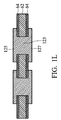
- FIG. 1L shows a cross-sectional view of a thermoelectric substrate after metal plating of the TSVs performed in step 21 of FIG. 1 according to one or more embodiments of the present disclosure.
- FIG. 1M shows a cross-sectional view of a pair of thermoelectric elements bonded to a thermoelectric substrate after step 22 of FIG. 1 according to one or more embodiments of the present disclosure.
- FIG. 1N shows a cross-sectional view of thermoelectric elements of a thermoelectric substrate bonded to the LED emitter substrate in the cavity of the LED emitter substrate according to one or more embodiments of the present disclosure.
- FIG. 2 shows a cross-sectional view of a LED component integrating a vertical LED die with a thermoelectric device using the method of FIG. 1 according to one or more embodiments of the present disclosure.
- FIG. 3 shows a cross-sectional view of a LED component integrating a face-up LED die with a thermoelectric device using the method of FIG. 1 according to one or more embodiments of the present disclosure.
- spatially relative terms such as “beneath,” “below,” “lower,” “above,” “upper” and the like, may be used herein for ease of description to describe one element or feature's relationship to another element(s) or feature(s) as illustrated in the figures. It will be understood that the spatially relative terms are intended to encompass different orientations of the device in use or operation in addition to the orientation depicted in the figures. For example, if the device in the figures is turned over, elements described as being “below” or “beneath” other elements or features would then be oriented “above” the other elements or features. Thus, the exemplary term “below” can encompass both an orientation of above and below. The device may be otherwise oriented (rotated 90 degrees or at other orientations) and the spatially relative descriptors used herein may likewise be interpreted accordingly.
- FIG. 1 shows a flowchart of a method 10 for fabricating a semiconductor LED component with an integrated thermoelectric device according to one or more embodiments of the present disclosure.
- Method 10 integrates an LED die bonded on an LED emitter substrate with thermoelectric elements bonded to a thermoelectric substrate.
- the thermoelectric elements and the thermoelectric substrate are positioned in a trench or cavity etched in the downward facing surface of the LED emitter substrate.
- the LED die is bonded to the upward facing surface of the LED emitter substrate opposite the thermoelectric elements in the trench or cavity. Heat from the LED die is carried away by the thermoelectric elements through thermal vias in the LED emitter substrate to facilitate cooling of the LED die.
- Method 10 is explained with reference to integrating gallium nitride (GaN) LEDs with thermoelectric elements using a silicon substrate as the LED emitter substrate. Alternatively, method 10 may be applied to LEDs or emitter substrates of different materials.
- GaN gallium nitride
- epitaxial layers for fabricating the LED die are deposited on a wafer of growth substrate having a lattice structure similar to the lattice structure of the LED material.
- the epitaxial layers are made of gallium nitride (GaN).
- GaN gallium nitride
- epitaxial layers of other materials are used.
- the epitaxial layers may be deposited by processes such as metal organic chemical vapor deposition (MOCVD) or other deposition processes.
- MOCVD metal organic chemical vapor deposition
- the deposited epitaxial layers may include an n-doped GaN layer (n-GaN), a multiple quantum well (MQW) active layer, a p-doped GaN layer (p-GaN), and a p-contact metal layer.
- LED dies may have different configurations and different processing steps depending on how the n-doped layer is electrically accessed.
- p-contacts and n-contacts for electrically accessing the p-GaN layer and the n-GaN layer of the LED are located on opposite sides of the LED.
- a face-up LED where contact metallization for the p-GaN layer and the n-GaN layer are both on the top side of the LED, portions of the p-GaN layer and the active layer are etched to expose the n-GaN layer for forming an n-contact metallization.
- an LED emitter substrate is provided.
- the LED emitter substrate is a silicon substrate.
- the LED emitter substrate may include other semiconductor materials.
- the silicon substrate has high thermal conductivity to improve thermal dissipation of the LED die that will be bonded to the upward facing surface of the silicon substrate.
- the silicon substrate will be deposited with a p-electrode and an n-electrode for connecting to the p-contact and the n-contact of the epitaxial layers of the LED die.
- the silicon substrate will be deposited with bonding areas for bonding to the LED die and to the thermoelectric elements.
- the bonding area for bonding to the LED die may be an extension of one of the p-electrode and n-electrode.
- the silicon substrate will be etched through a wet etch process or a dry etch process to form a trench or cavity for bonding to the thermoelectric elements
- FIG. 1A shows a cross-sectional view of a silicon substrate after deposition of a wet etch barrier according to one or more embodiments of the present disclosure.
- a wet etch barrier layer 101 is first deposited on both surfaces of silicon substrate 38 .
- FIG. 1B shows a cross-sectional view of a silicon substrate with an opening in the wet etch barrier layer according to one or more embodiments of the present disclosure.
- an opening 103 is made through wet etch barrier layer 101 on one surface of silicon substrate 38 in an area where a cavity is to be etched into silicon substrate 38 .
- the cavity defines an area for integrating the thermoelectric elements and the thermoelectric substrate to silicon substrate 38 .
- the surface of silicon substrate 38 into which the cavity is etched is referred to as the downward facing surface of silicon substrate 38 .
- the other surface is referred to as the upward facing surface of silicon substrate 38 .
- a trench or cavity is etched into the downward facing surface of the silicon substrate using an etching process.
- the etching process may be a wet etch process for forming a cavity with sloping sidewalls.
- the etching process may be a dry etch process for forming a cavity with vertical sidewalls.
- FIG. 1C shows a cross-sectional view of a silicon substrate with a cavity formed by a wet etch process according to one or more embodiments of the present disclosure.
- a cavity 54 is etched into a surface of silicon substrate 38 to create a space for positioning the thermoelectric elements and the thermoelectric substrate used to support the thermoelectric elements.
- Cavity 54 is sufficiently deep to allow the thermoelectric elements to be located as close as possible to the LED die to be bonded to the upward facing surface of silicon substrate 38 for more effective cooling of the LED die.
- cavity 54 may not be too deep so as to avoid weakening the structural integrity of silicon substrate 38 . Accordingly, in the present embodiment, areas of silicon substrate 38 remain between the bottom of cavity 54 and the upward facing surface where the LED die is to be bonded.
- FIG. 1D shows a cross-sectional view of a silicon substrate with a cavity after step 13 of FIG. 1 according to one or more embodiments of the present disclosure.
- vias are etched in the silicon substrate for forming through-silicon vias (TSVs) using an etching process such as dry etching.
- TSVs may be formed in the silicon substrate using laser drilling.
- the TSVs may be thermal TSVs between the bottom of the trench or cavity and the upward facing surface of the silicon substrate close to where the LED die is to be bonded.
- the end of a thermal TSV at the bottom of the cavity connects to a thermal element positioned in the cavity.
- the other end of the thermal TSV at the upper facing surface of the silicon substrate may connect to another thermal TSV through a metal interconnect.
- the thermal TSVs act as an extension of the thermoelectric elements to channel heat away from the LED die to the thermoelectric elements.
- each pair of thermal TSVs may connect to a p-type and an n-type thermoelectric element.
- power is applied to the thermoelectric elements to positively bias the n-type thermoelectric element relative to the p-type thermoelectric element, electrons of the n-type thermoelectric element and holes of the p-type thermoelectric element move through the thermal TSVs in the direction from the LED die toward the thermoelectric elements. The direction of the flow of the charge carriers removes heat from the LED die.
- the metallic interconnects between each pair of n-type and p-type thermoelectric elements provide a conductive path for the current to move from the n-type thermoelectric element to the p-type thermoelectric element.
- thermal TSVs there may also be electrical TSVs between the downward facing surface and the upward facing surface of the silicon substrate in areas of the silicon substrate other than the cavity.
- the electrical TSVs provide electrical paths for supplying power from the downward facing surface of the silicon substrate to the LED die disposed on the upward facing surface.
- FIG. 1E shows a cross-sectional view of a silicon substrate etched with thermal and electrical TSVs after step 14 of FIG. 1 according to one or more embodiments of the present disclosure.
- Thermal TSVs 107 are formed between the bottom of cavity 54 and the upward facing surface of silicon substrate 38 .
- electrical TSVs 109 are formed between the two surfaces of silicon substrate 38 in areas of silicon substrate 38 other than the cavity 54 .
- a dielectric layer such as SiO 2 is deposited on both the upward and downward facing surfaces of the silicon substrate and also on the walls of the TSVs.
- the dielectric layer may be made of silicon nitrite (Si 3 N 4 ), or silicon carbide, (SiC).
- Deposit of the dielectric layer may be through a chemical vapor deposition process. The dielectric layer electrically isolates metal layer of the TSVs from the silicon substrate and also prevents diffusion of the metal layer into the silicon substrate.
- FIG. 1F shows a cross-sectional view of a silicon substrate with a dielectric layer after step 15 of FIG. 1 according to one or more embodiments of the present disclosure.
- a dielectric layer 40 is deposited on the inside wall surfaces of thermal TSVs 107 and electrical TSVs 109 , and also on both surfaces of silicon substrate 38 .
- a photolithography process is used to define openings for metal plating of the TSVs and a metal layer is deposited over the dielectric layer to form surface metal plating for the TSVs.
- the metal layer also fills the TSVs to complete the fabrication of the TSVs.
- metal interconnects are formed between pairs of thermal TSVs at their upward facing surface.
- FIG. 1G shows a cross-sectional view of a silicon substrate after metal plating of the TSVs performed in step 16 of FIG. 1 according to one or more embodiments of the present disclosure.
- a surface metal plating 113 is formed at the bottom of the cavity 54 for bonding to their respective thermoelectric elements.
- a metal interconnect 56 is disposed to form a bridge between the two thermal TSVs 107 .
- the two thermal TSVs 107 may be bonded to a p-type thermal element and an n-type thermal element.
- metal interconnect 56 connects in series a pair of p-type and n-type thermal elements.
- electrical TSVs 109 have surface metal plating 115 on the upward facing surface of silicon substrate 38 to form contact areas for electrically connecting to the LED die.
- surface metal plating 117 is formed to provide electrodes for connecting to power supplied from package pins or for connecting to other devices.
- a second dielectric layer such as SiO 2 is deposited on the upward facing surface of the silicon substrate and patterned through a photolithography process to cover the metal interconnect between pairs of thermal TSVs.
- a photolithography process may be used to define an area over the second dielectric layer and a surface metal plating on the upward facing surface of an electric TSV.
- a second metal layer is deposited over the defined area on the upward facing surface of the silicon substrate to form a secondary surface metal plating for bonding to the vertical LED die.
- FIG. 1H shows a cross-sectional view of a silicon substrate after deposition of a second dielectric layer to cover a metal interconnect between a pair of thermal TSVs performed in step 17 of FIG. 1 according to one or more embodiments of the present disclosure.
- Second dielectric layer 119 electrically isolates metal interconnect 56 from the LED die that will be bonded to the upward facing surface of silicon substrate 38 .
- Second dielectric layer 119 is also extended to cover first dielectric layer 40 between surface metal plating 115 of two electrical TSVs 109 on the upward facing surface of silicon substrate 38 .
- Second dielectric layer 119 may be made of the same material as first dielectric layer 40 and may be treated as an extension of first dielectric layer 40
- FIG. 1I shows a cross-sectional view of a silicon substrate after deposition of a second metal layer to form a secondary surface metal plating performed in step 17 of FIG. 1 according to one or more embodiments of the present disclosure.
- a secondary surface metal plating 121 is deposited over surface metal plating 115 of electrical TSV 109 and over second dielectric layer 119 on the upward facing surface of silicon substrate 38 .
- Secondary surface metal plating 121 serves as a contact for bonding an LED die to the upward facing surface of silicon substrate 38 .
- Secondary surface metal plating 121 also electrically connects to surface metal plating 115 of electrical TSV 109 to supply power to the LED die.
- secondary surface metal plating 121 may also serve as a thermal contact to conduct heat away from the LED die.
- Secondary surface metal plating 121 may be made of the same metal as surface metal plating 115 and may be treated as an extension of surface metal plating 115 .
- an LED emitter substrate such as silicon substrate 38 is fabricated to include a bonding area made of a secondary surface metal plating 121 on the upward facing surface of the LED emitter substrate for bonding to an LED die.
- the LED emitter substrate also has cavity 54 on the downward facing surface of the LED emitter substrate.
- Thermal TSVs 107 between the bottom of cavity 54 and the upward facing surface of the LED emitter substrate channel heat from the LED die to thermoelectric elements.
- Thermal TSVs 107 also provide surface metal plating 113 as bonding areas for bonding to the thermoelectric elements positioned in cavity 54 .
- electrical TSVs 109 are disposed in the LED emitter substrate for supplying power to the LED die.
- Other microelectronic devices and supporting circuitries may also be formed in the LED emitter substrate to electrically connect the LED die to other devices or to external package pins.
- thermoelectric substrate may have a similar structure as the LED emitter substrate.
- the thermoelectric substrate is a silicon substrate.
- the thermoelectric substrate may include other semiconductor materials.
- the thermoelectric substrate provides a substrate for bonding thermoelectric elements and will be disposed with TSVs to provide both electrical connections and heat dissipation channels for the thermoelectric elements.
- a dielectric layer such as SiO 2 is deposited on both surfaces of the thermoelectric substrate. Deposit of the dielectric layer may be through a chemical vapor deposition process. The dielectric layer electrically isolates metal surface plating that will be deposited for the TSVs from the thermoelectric substrate and also prevents diffusion of the metal layer into the thermoelectric substrate.
- FIG. 1J shows a cross-sectional view of a thermoelectric substrate with deposition of a dielectric layer after step 18 of FIG. 1 according to one or more embodiments of the present disclosure.
- a dielectric layer 64 is deposited on both surfaces of a silicon substrate 62 of a thermoelectric substrate.
- vias are etched in the thermoelectric substrate and the dielectric layer for forming TSVs using an etching process such as dry etching.
- vias may be formed in the thermoelectric substrate using laser drilling.
- the TSVs may be thermal TSVs that bond with the thermoelectric elements disposed on one side of the thermoelectric substrate to conduct heat from the thermoelectric elements to the other side of the thermoelectric substrate.
- the thermal TSVs may open to the ambient air for convective cooling or may be connected with a heat sink for conductive cooling.
- thermoelectric interconnect between the n-type thermoelectric element of a first thermoelectric pair and the p-type thermoelectric element of an adjacent thermoelectric pair. In this way, pairs of thermoelectric elements may be connected in series for enhanced cooling of the LED die.
- thermoelectric substrate In addition to the thermal TSVs, there are also electrical TSVs between the two sides of the thermoelectric substrate for supplying power to the thermoelectric elements from electrodes disposed on the side of the thermoelectric substrate not having the thermoelectric elements.
- FIG. 1K shows a cross-sectional view of a thermoelectric substrate etched with electrical TSVs after step 20 of FIG. 1 according to one or more embodiments of the present disclosure.
- Electrical TSVs 123 are formed between the two surfaces of the thermoelectric substrate that includes dielectric layer 64 and silicon substrate 62 .
- a metal layer is deposited over the dielectric layer to form surface metal plating for the TSVs.
- the metal layer also fills the TSVs to complete the fabrication of the TSVs.
- a barrier layer such as titanium may be deposited on the dielectric layer and a seed metal layer such as copper may be deposited on the barrier layer.
- a photoresist layer may be laminated on the seed metal layer and patterned in a photo-lithography process to define areas for the surface metal plate.
- a metal layer such as copper may then be deposited through metal plating over the seed metal layer to form the surface metal plating for the TSVs and to fill the via openings.
- FIG. 1L shows a cross-sectional view of a thermoelectric substrate after metal plating of the TSVs performed in step 21 of FIG. 1 according to one or more embodiments of the present disclosure.
- electrical TSVs 123 On one side of the thermoelectric substrate, electrical TSVs 123 have surface metal plating 125 to form contact areas for bonding to and electrically connecting with thermoelectric elements.
- surface metal plating 127 of electrical TSVs 123 provides electrodes for connecting the thermoelectric elements to power supplies.
- thermoelectric elements are bonded to the thermoelectric substrate through the surface metal plating of thermal TSVs and electrical TSVs.
- the thermoelectric elements include alternating p-type and n-type semiconductor elements arranged in pairs.
- the side of the thermoelectric elements bonded to the thermoelectric substrate is referred to as the hot end of the thermoelectric element because the thermoelectric elements are electrically biased to transfer heat to this end. Bonding of the thermoelectric elements to the thermoelectric substrate may be performed by a soldering process.
- FIG. 1M shows a cross-sectional view of a pair of thermoelectric elements bonded to a thermoelectric substrate after step 22 of FIG. 1 according to one or more embodiments of the present disclosure.
- a pair of thermoelectric elements including a p-type thermoelectric element 58 and an n-type thermoelectric element 60 is bonded to surface metal plating 125 of electrical TSVs 123 of the thermoelectric substrate through a solder layer 129 .
- Another solder layer 129 is deposited on the side of p-type thermoelectric element 58 and n-type thermoelectric element 60 not bonded to the thermoelectric substrate. This solder layer will be used to bond the thermoelectric elements to the LED emitter substrate.
- thermoelectric elements and the thermoelectric substrate are positioned at the bottom of the trench or cavity of the LED emitter substrate so that the end of the thermoelectric elements not bonded to the thermoelectric substrate is bonded to the thermal TSVs of the LED emitter substrate.
- the side of the thermoelectric elements bonded to the thermal TSVs of the LED emitter substrate is referred to as the cold end of the thermoelectric elements because the thermoelectric elements are biased to remove heat from this side to the hot end.
- FIG. 1N shows a cross-sectional view of thermoelectric elements of a thermoelectric substrate bonded to the LED emitter substrate in the cavity of the LED emitter substrate according to one or more embodiments of the present disclosure.
- P-type thermoelectric element 58 and n-type thermoelectric element 60 on the thermoelectric substrate are bonded to surface metal plating 113 of thermal TSVs 107 of the LED emitter substrate through a solder layer 129 .
- metal interconnect 56 forms a bridge between the two thermal TSVs 107 to connect the pair of p-type thermoelectric element 58 and n-type thermoelectric element 60 in series.
- thermoelectric substrate supply power to the thermoelectric elements from power supplies connected to surface metal plating 127 of electrical TSVs 123 from the downward facing surface of the thermoelectric substrate. Electrical TSVs 123 also channel heat away from the hot end of the thermoelectric elements.
- the LED die from step 11 is bonded to the upward facing surface of the LED emitter substrate opposite the trench or cavity containing the thermoelectric elements.
- the LED die may be bonded to the secondary surface metal plating of the LED emitter substrate where the secondary surface metal plating also has a reflective layer to reflect upward light from the active layer of the LED die.
- bonding to the LED emitter substrate may be through the p-GaN layer or through a heavily doped silicon wafer that is connected to the p-GaN layer. Bonding of the vertical GaN LED die to the secondary surface metal plating of the LED emitter substrate also electrically connects the p-GaN layer.
- the growth substrate of the vertical LED die may be removed to improve thermal dissipation because the growth substrate typically has low thermal conductivity. For a sapphire growth substrate, removal may be by means of a laser lift-off (LLO) technique. For a silicon-based growth substrate, removal may be by means of dry or wet etching techniques. Alternatively, the growth substrate may be grinded and polished to reduce its thickness.
- LLO laser lift-off
- n-GaN layer Removal of the growth substrate from the LED die exposes the n-GaN layer.
- the exposed n-GaN layer will be connected to power through an electrical TSV of the LED emitter substrate.
- Detailed structure of a vertical LED die bonded to a LED emitter substrate that is bonded with thermoelectric elements will be discussed in FIG. 2 .
- bonding to the LED emitter substrate may be through the growth substrate. Contrary to the vertical GaN LED die, bonding of the face-up LED die to the secondary surface metal plating of the LED emitter substrate does not electrically connect the p-GaN layer. Instead, electrical access to the p-GaN layer and to the n-GaN layer is from the non-bonding side of the LED die Detailed structure of a face-up LED die bonded to a LED emitter substrate that is bonded with thermoelectric elements will be discussed in FIG. 3 .
- the LED die is electrically connected to surface metal plating of electrical TSVs on the LED emitter substrate.
- the p-GaN layer has already been connected to the LED emitter substrate through the secondary surface metal plating used to bond the LED die. Therefore, only the connection to the n-GaN layer needs to be made by connecting an n-contact metal layer of the LED die to a surface metal plating of an electrical TSV.
- connection from both an n-GaN contact metallization and the p-contact metal layer are made to surface metal plating of their electrical TSVs.
- electrical connections are made by depositing bonding wires.
- Alternative embodiments include forming micro-interconnects through a photolithography process. To complete the LED fabrication process, a phosphor coating is deposited on the LED die to change the wavelength of the emitted light. In addition, lens molding is formed on the phosphor coating to further shape an emission pattern of the emitted light.
- FIG. 2 shows a cross-sectional view of an LED component integrating a vertical LED die with a thermoelectric device using the method of FIG. 1 according to one or more embodiments of the present disclosure.
- the epitaxial layers of the LED die include an n-doped GaN layer 30 or a layer of other n-type semiconductor materials.
- a multiple quantum well (MQW) active layer 32 is deposited on n-doped GaN layer 30 .
- MQW active layer 32 may include alternating (or periodic) layers of GaN and indium gallium nitride (InGaN).
- InGaN indium gallium nitride
- MQW active layer 32 includes at least 7 alternating layers of GaN and InGaN.
- a p-doped GaN layer 34 or a layer of other p-type semiconductor materials is deposited on MQW active layer 32 .
- a heavily doped silicon layer 36 is deposited on p-doped GaN layer 34 .
- Heavily doped silicon layer 36 may include metals that have good conductive properties.
- a P/N junction (or a P/N diode) is essentially formed from MQW active layer 32 being disposed between n-doped GaN layer 30 and p-doped GaN layer 34 .
- an electrical voltage or electrical charge
- electrical current flows through the LED, causing MQW active layer 32 to emit light.
- the color of the light emitted by MQW active layer 32 is associated with the wavelength of the light, which may be tuned by varying the composition and structure of the materials that make up MQW active layer 32 .
- the LED emitter substrate includes a silicon substrate 38 layer that is sandwiched between two isolation or dielectric layers 40 .
- Isolation layers 40 include dielectric materials such as SiO 2 .
- the LED emitter substrate includes a p-channel electrical TSV 42 disposed through isolation layers 40 and silicon substrate layer 38 .
- P-channel electrical TSV 42 electrically connects to a LED bonding pad 44 disposed on the upward facing surface of isolation layers 40 .
- LED bonding pad 44 includes secondary surface metal plating 121 and surface metal plating 115 as shown in FIGS. 1I and 1N .
- LED bonding pad 44 and p-channel electrical TSV 42 provide electrical access to p-doped GaN layer 34 through heavily doped silicon layer 36 .
- LED bonding pad 44 also serves as a thermal contact to conduct heat away from the LED die as well as a contact for bonding the LED die to the LED emitter substrate.
- LED bonding pad 44 has reflective function or a reflective layer to reflect upward light from MQW active layer 32 .
- LED bonding pad 44 includes metals with good conductive properties, both electrical and thermal, and good bonding property such as gold, gold alloy, copper, copper alloy, nickel, nickel alloy, platinum, platinum alloy, titanium, titanium alloy, or combinations thereof.
- the LED emitter substrate also includes an n-channel electrical TSV 46 disposed through isolation layers 40 and silicon substrate layer 38 .
- N-channel electrical TSV 46 electrically connects to an n-contact 48 that is a surface metal plating disposed on the upward facing surface of isolation layers 40 .
- N-contact 48 connects to n-doped GaN layer 30 through an n-contact bonding wire 49 . Therefore, n-channel electrical TSV 46 , n-contact 48 , and n-contact bonding wire 49 provide electrical access to n-doped GaN layer 30 .
- the LED emitter substrate further includes one or more p-type thermal TSVs 50 and n-type thermal TSVs 52 disposed between the bottom of a cavity 54 on the downward facing surface of the silicon substrate 38 and isolation layers 40 .
- P-type thermal TSVs 50 and n-type thermal TSVs 52 help to channel heat from LED bonding pad 44 to thermoelectric elements disposed in the cavity 54 .
- Metallic interconnects 56 are disposed between adjacent P-type thermal TSVs 50 and n-type thermal TSVs 52 to provide a conductive path for current to flow from n-type thermal TSVs 52 to p-type thermal TSVs 50 .
- P-type thermal TSVs 50 are connected to the cold end of p-type thermoelectric elements 58 disposed on the bottom of cavity 54 .
- n-type TSVs 52 are connected to the cold end of n-type thermoelectric elements 60 disposed on the bottom of cavity 54 .
- P-type thermoelectric elements 58 and n-type thermoelectric elements 60 are arranged in
- thermoelectric substrate disposed in the cavity 54 .
- the thermoelectric substrate has a silicon substrate layer 62 sandwiched between dielectric layers 64 , in a structure similar to that of the LED emitter substrate.
- the thermoelectric substrate also includes a p-type electrical TSV 66 and an n-type electrical TSV 68 patterned to extend through silicon substrate 62 and dielectric layers 64 and disposed close to the outer edges of the thermoelectric substrate.
- One end of p-type electrical TSV 66 connects to a p-type bonding pad 70 which connects with the hot end of an outermost one of p-type thermoelectric elements 58 .
- p-type electrical TSV 66 connects to a p-type electrode 72 for supplying power to the thermoelectric elements.
- n-type electrical TSV 68 connects to an n-type bonding pad 74 which connects with the hot end of an outermost one of n-type thermoelectric elements 60 .
- the other end of n-type electrical TSV 68 connects to an n-type electrode 76 for supplying power to the thermoelectric elements.
- thermoelectric substrate includes a thermal TSV 78 and a thermoelectric interconnect 80 .
- Thermoelectric interconnect 80 connects the hot end of an inner one of p-type thermoelectric elements 58 with the hot end of an inner one of adjacent n-type thermoelectric elements 60 to provide a conductive path for current to flow from p-type thermoelectric elements to n-type thermoelectric elements.
- Thermoelectric interconnect 80 also connects with thermal TSV 78 to channel heat away from the hot end of the thermoelectric elements.
- thermal TSV 78 relies on convection cooling to dissipate heat to the ambient air near the downward facing surface of the thermal substrate.
- thermal TSV 78 may be connected to a heat sink.
- the network of electrodes, boding pads, TSVs, and interconnects electrically connects the alternating arrangement of p-type thermoelectric elements 58 and n-type thermoelectric elements 60 in series. For example, when a positive voltage is applied to n-type electrode 76 and p-type electrode 72 is tied to ground, current flows from n-type electrode 76 through n-type electrical TSV 68 and through n-type bonding pad 74 to the hot end of the outermost one of n-type thermoelectric elements 60 .
- thermoelectric interconnect 80 to the inner one of n-type thermoelectric elements 60 .
- Current then flows from the inner one of n-type thermoelectric elements 60 to the outermost one of p-type thermoelectric elements 58 through a second set of n-type thermal TSVs 52 , metallic interconnect 56 and p-type thermal TSVs 50 .
- current flows out of the hot end of the outermost one of p-type thermoelectric elements 58 through p-type bonding pad 70 , and through p-type electrical TSV 66 , to p-type electrode 72 to close the circuit.
- n-type electrode 76 when n-type electrode 76 is positively biased relative to p-type electrode 72 , current flows out of the cold end of n-type thermoelectric elements 60 and into the cold end of p-type thermoelectric elements 58 . Because the electrons of n-type thermoelectric elements 60 move opposite the direction of the current, electrons in n-type thermoelectric elements 60 move from the cold end to the hot end of n-type thermoelectric elements 60 , away from the LED die. Similarly, because the holes of p-type thermoelectric elements 58 move in the direction of the current, holes in p-type thermoelectric elements 58 also move from the cold end to the hot end of p-type thermoelectric elements 58 , away from the LED die.
- thermoelectric interconnect 80 connects with hot end of p-type thermoelectric elements 58 and n-type thermoelectric elements 60 to channel heat into thermal TSV 78 and into ambient air on the downward facing surface of the thermoelectric substrate.
- P-layer electrode 82 and n-layer electrode 84 which are surface metal plating 117 of electrical TSVs as shown in FIGS. 1G , 1 H, 1 I, and 1 N, are disposed on the downward facing surface of the silicon substrate to connect to external package pins for supplying power to the LED die.
- power is supplied to p-doped GaN layer 34 through p-layer electrode 82 , p-channel electrical TSV 42 , LED bonding pad 44 , and heavily doped silicon layer 36 .
- power is supplied to n-doped GaN layer 30 through n-layer electrode 84 , n-channel electrical TSV 46 , n-contact 48 , and n-contact bonding wire 49 .
- Light from MQW active layer 32 is extracted from the upward side of the LED die.
- a phosphor coating and a lens molding 88 are deposited on the LED die to shape the spectra and the emission pattern of the vertical LED die.
- FIG. 3 shows a cross-sectional view of a LED component integrating a face-up LED die with a thermoelectric device using the method of FIG. 1 according to one or more embodiments of the present disclosure.
- contact metallization for the p-doped GaN layer and the n-doped GaN layer are both located on upward top side of the LED. Electrical access to p-doped GaN layer 34 is provided through a p-contact metal layer 37 .
- the LED emitter substrate includes a p-contact 94 , a p-channel electrical TSV 92 , and a p-layer electrode 96 to supply power to p-doped GaN layer 34 through a p-contact bonding wire 98 and p-contact metal layer 37 .
- P-contact 94 is surface metal plating 115 of electrical TSVs shown in FIGS. 1G and 1H .
- P-layer electrode 96 is surface metal plating 117 of electrical TSVs shown in FIGS. 1G and 1H .
- the LED emitter substrate has an n-contact 48 , an n-channel electrical TSV 46 , and an n-layer electrode 84 for supplying power to n-doped GaN layer 30 through an n-contact bonding wire 49 .
- portions of the p-doped GaN layer 34 and MQW active layer 32 are etched to form an n-contact metallization 90 to provide electrical access to n-doped GaN layer 30 .
- the LED emitter substrate includes an n-contact 48 , an n-channel electrical TSV 46 , and an n-layer electrode 84 of the LED emitter substrate to supply power to n-doped GaN layer 30 through an n-contact bonding wire 49 and n-contact metallization 90 .
- a growth substrate 29 of the face-up LED die is bonded to the LED emitter substrate through a bonding pad 100 that also serves as a thermal contact to conduct heat away from the LED die.
- LED bonding pad 100 may include secondary surface metal plating 121 as shown in FIGS. 1I and 1N .
- LED bonding pad 100 has a reflective function or a reflective layer to reflect upward light from MQW active layer 32 .
- the LED emitter substrate includes p-type thermal TSVs 50 and n-type thermal TSVs 52 connected respectively to the cold end of p-type thermoelectric elements 58 and n-type thermoelectric elements 60 disposed in an alternating arrangement on the bottom of a cavity 54 .
- the hot end of p-type thermoelectric elements 58 and n-type thermoelectric elements 60 connect with a thermoelectric substrate.
- the thermoelectric substrate has a network of electrodes, boding pads, TSVs, and interconnects to electrically connect the alternating p-type thermoelectric elements 58 and n-type thermoelectric elements 60 in series.
- a light emitting diode (LED) component includes an LED emitter substrate having an upward facing surface and a downward facing surface.
- the LED emitter substrate has a cavity in the downward facing surface of the LED emitter substrate and thermal vias that extend from a bottom of the cavity to an area close to an upward facing surface of the LED emitter substrate.
- the LED component also includes thermoelectric elements disposed in the cavity. The thermoelectric elements connect with their corresponding thermal vias of the LED emitter substrate.
- the device further includes a thermoelectric substrate in the cavity.
- the thermoelectric substrate has electrical vias and bonding pads to electrically connect to the thermoelectric elements.
- the device further includes an LED die having doped layers positioned on the upward facing surface of the LED emitter.
- a light emitting diode (LED) component has a downward facing surface and an upward facing surface.
- the LED component includes a cavity in the downward facing surface of the LED component.
- the LED component also includes thermal vias extending from a bottom of the cavity to an area close to an upward facing surface of the LED component.
- the LED component further includes an LED die disposed on the upward facing surface.
- the LED component further includes thermoelectric elements in the cavity. The thermoelectric elements connect with the thermal vias such that a direction of flow of charge carriers of the thermoelectric elements is away from the LED die to remove heat from the LED die.
- a method for fabricating a light emitting diode (LED) component includes providing an LED emitter substrate of a first semiconductor material.
- the LED emitter substrate has a downward facing surface and an upward facing surface.
- the method also includes etching a cavity in the downward facing surface of the LED emitter substrate.
- the method further includes patterning thermal vias in the LED emitter substrate such that the thermal vias extend from a bottom of the cavity to an area close to an upward facing surface of the LED emitter substrate.
- the method further includes providing a thermoelectric substrate of a second semiconductor material.
- the method further includes patterning vias in the thermoelectric substrate.
- the method further includes bonding thermoelectric elements to the vias in the thermoelectric substrate.
- the method further includes bonding the thermoelectric elements to the vias in the LED emitter substrate from inside the cavity.
- the method further includes bonding an LED die to the upward facing surface of the LED emitter substrate such that the LED die is opposite the cavity in the LED emitter substrate.
Abstract
Description
Claims (20)
Priority Applications (2)
| Application Number | Priority Date | Filing Date | Title |
|---|---|---|---|
| US12/946,453 US8519409B2 (en) | 2010-11-15 | 2010-11-15 | Light emitting diode components integrated with thermoelectric devices |
| CN201110087878.XA CN102468409B (en) | 2010-11-15 | 2011-04-06 | Light emitting diode components integrated with thermoelectric devices and method of manufacturing the same |
Applications Claiming Priority (1)
| Application Number | Priority Date | Filing Date | Title |
|---|---|---|---|
| US12/946,453 US8519409B2 (en) | 2010-11-15 | 2010-11-15 | Light emitting diode components integrated with thermoelectric devices |
Publications (2)
| Publication Number | Publication Date |
|---|---|
| US20120119246A1 US20120119246A1 (en) | 2012-05-17 |
| US8519409B2 true US8519409B2 (en) | 2013-08-27 |
Family
ID=46046998
Family Applications (1)
| Application Number | Title | Priority Date | Filing Date |
|---|---|---|---|
| US12/946,453 Active 2031-11-10 US8519409B2 (en) | 2010-11-15 | 2010-11-15 | Light emitting diode components integrated with thermoelectric devices |
Country Status (2)
| Country | Link |
|---|---|
| US (1) | US8519409B2 (en) |
| CN (1) | CN102468409B (en) |
Families Citing this family (3)
| Publication number | Priority date | Publication date | Assignee | Title |
|---|---|---|---|---|
| CN103500729B (en) * | 2013-10-18 | 2015-10-14 | 中国科学院上海微系统与信息技术研究所 | Silicon adapter plate structure and wafer level manufacture method thereof |
| CN107833951B (en) * | 2017-11-28 | 2020-12-22 | 浙江清华柔性电子技术研究院 | LED packaging method |
| DE102018101815A1 (en) * | 2018-01-26 | 2019-08-01 | Osram Opto Semiconductors Gmbh | Optoelectronic semiconductor component and method for producing an optoelectronic semiconductor component |
Citations (27)
| Publication number | Priority date | Publication date | Assignee | Title |
|---|---|---|---|---|
| US5391917A (en) | 1993-05-10 | 1995-02-21 | International Business Machines Corporation | Multiprocessor module packaging |
| US5510298A (en) | 1991-09-12 | 1996-04-23 | Texas Instruments Incorporated | Method of interconnect in an integrated circuit |
| US5767001A (en) | 1993-05-05 | 1998-06-16 | Siemens Aktiengesellschaft | Process for producing semiconductor components between which contact is made vertically |
| US5998292A (en) | 1997-11-12 | 1999-12-07 | International Business Machines Corporation | Method for making three dimensional circuit integration |
| US6184060B1 (en) | 1996-10-29 | 2001-02-06 | Trusi Technologies Llc | Integrated circuits and methods for their fabrication |
| US6322903B1 (en) | 1999-12-06 | 2001-11-27 | Tru-Si Technologies, Inc. | Package of integrated circuits and vertical integration |
| US6448168B1 (en) | 1997-09-30 | 2002-09-10 | Intel Corporation | Method for distributing a clock on the silicon backside of an integrated circuit |
| US6465892B1 (en) | 1999-04-13 | 2002-10-15 | Oki Electric Industry Co., Ltd. | Interconnect structure for stacked semiconductor device |
| US6538333B2 (en) | 2000-06-16 | 2003-03-25 | Chartered Semiconductor Manufacturing Ltd. | Three dimensional IC package module |
| US6599778B2 (en) | 2001-12-19 | 2003-07-29 | International Business Machines Corporation | Chip and wafer integration process using vertical connections |
| US6664129B2 (en) | 1996-10-29 | 2003-12-16 | Tri-Si Technologies, Inc. | Integrated circuits and methods for their fabrication |
| US6800930B2 (en) | 2002-07-31 | 2004-10-05 | Micron Technology, Inc. | Semiconductor dice having back side redistribution layer accessed using through-silicon vias, and assemblies |
| US6841883B1 (en) | 2003-03-31 | 2005-01-11 | Micron Technology, Inc. | Multi-dice chip scale semiconductor components and wafer level methods of fabrication |
| US6924551B2 (en) | 2003-05-28 | 2005-08-02 | Intel Corporation | Through silicon via, folded flex microelectronic package |
| US6962872B2 (en) | 2002-12-09 | 2005-11-08 | International Business Machines Corporation | High density chip carrier with integrated passive devices |
| US7049170B2 (en) | 2003-12-17 | 2006-05-23 | Tru-Si Technologies, Inc. | Integrated circuits and packaging substrates with cavities, and attachment methods including insertion of protruding contact pads into cavities |
| US7060601B2 (en) | 2003-12-17 | 2006-06-13 | Tru-Si Technologies, Inc. | Packaging substrates for integrated circuits and soldering methods |
| US7071546B2 (en) | 2002-01-16 | 2006-07-04 | Alfred E. Mann Foundation For Scientific Research | Space-saving packaging of electronic circuits |
| US7111149B2 (en) | 2003-07-07 | 2006-09-19 | Intel Corporation | Method and apparatus for generating a device ID for stacked devices |
| US7122912B2 (en) | 2004-01-28 | 2006-10-17 | Nec Electronics Corporation | Chip and multi-chip semiconductor device using thereof and method for manufacturing same |
| US7157787B2 (en) | 2002-02-20 | 2007-01-02 | Intel Corporation | Process of vertically stacking multiple wafers supporting different active integrated circuit (IC) devices |
| US7193308B2 (en) | 2003-09-26 | 2007-03-20 | Seiko Epson Corporation | Intermediate chip module, semiconductor device, circuit board, and electronic device |
| US7262495B2 (en) | 2004-10-07 | 2007-08-28 | Hewlett-Packard Development Company, L.P. | 3D interconnect with protruding contacts |
| US7297574B2 (en) | 2005-06-17 | 2007-11-20 | Infineon Technologies Ag | Multi-chip device and method for producing a multi-chip device |
| US7335972B2 (en) | 2003-11-13 | 2008-02-26 | Sandia Corporation | Heterogeneously integrated microsystem-on-a-chip |
| US7633093B2 (en) * | 2003-05-05 | 2009-12-15 | Lighting Science Group Corporation | Method of making optical light engines with elevated LEDs and resulting product |
| US20100117113A1 (en) * | 2008-11-10 | 2010-05-13 | Foxsemicon Integrated Technology, Inc. | Light emitting diode and light source module having same |
Family Cites Families (3)
| Publication number | Priority date | Publication date | Assignee | Title |
|---|---|---|---|---|
| JP2003131191A (en) * | 2001-10-22 | 2003-05-08 | Matsushita Electric Ind Co Ltd | Field sequential color liquid crystal display device |
| JP2004296100A (en) * | 2003-03-25 | 2004-10-21 | Toyota Industries Corp | Organic el device and liquid crystal display device |
| JP2004342557A (en) * | 2003-05-19 | 2004-12-02 | Seiko Epson Corp | Lighting system and projection type display device |
-
2010
- 2010-11-15 US US12/946,453 patent/US8519409B2/en active Active
-
2011
- 2011-04-06 CN CN201110087878.XA patent/CN102468409B/en active Active
Patent Citations (35)
| Publication number | Priority date | Publication date | Assignee | Title |
|---|---|---|---|---|
| US5510298A (en) | 1991-09-12 | 1996-04-23 | Texas Instruments Incorporated | Method of interconnect in an integrated circuit |
| US5767001A (en) | 1993-05-05 | 1998-06-16 | Siemens Aktiengesellschaft | Process for producing semiconductor components between which contact is made vertically |
| US5391917A (en) | 1993-05-10 | 1995-02-21 | International Business Machines Corporation | Multiprocessor module packaging |
| US6664129B2 (en) | 1996-10-29 | 2003-12-16 | Tri-Si Technologies, Inc. | Integrated circuits and methods for their fabrication |
| US6184060B1 (en) | 1996-10-29 | 2001-02-06 | Trusi Technologies Llc | Integrated circuits and methods for their fabrication |
| US6639303B2 (en) | 1996-10-29 | 2003-10-28 | Tru-Si Technolgies, Inc. | Integrated circuits and methods for their fabrication |
| US6882030B2 (en) | 1996-10-29 | 2005-04-19 | Tru-Si Technologies, Inc. | Integrated circuit structures with a conductor formed in a through hole in a semiconductor substrate and protruding from a surface of the substrate |
| US6740582B2 (en) | 1996-10-29 | 2004-05-25 | Tru-Si Technologies, Inc. | Integrated circuits and methods for their fabrication |
| US6448168B1 (en) | 1997-09-30 | 2002-09-10 | Intel Corporation | Method for distributing a clock on the silicon backside of an integrated circuit |
| US5998292A (en) | 1997-11-12 | 1999-12-07 | International Business Machines Corporation | Method for making three dimensional circuit integration |
| US6465892B1 (en) | 1999-04-13 | 2002-10-15 | Oki Electric Industry Co., Ltd. | Interconnect structure for stacked semiconductor device |
| US6472293B2 (en) | 1999-04-13 | 2002-10-29 | Oki Electric Industry Co., Ltd. | Method for manufacturing an interconnect structure for stacked semiconductor device |
| US6322903B1 (en) | 1999-12-06 | 2001-11-27 | Tru-Si Technologies, Inc. | Package of integrated circuits and vertical integration |
| US6693361B1 (en) | 1999-12-06 | 2004-02-17 | Tru-Si Technologies, Inc. | Packaging of integrated circuits and vertical integration |
| US6538333B2 (en) | 2000-06-16 | 2003-03-25 | Chartered Semiconductor Manufacturing Ltd. | Three dimensional IC package module |
| US6599778B2 (en) | 2001-12-19 | 2003-07-29 | International Business Machines Corporation | Chip and wafer integration process using vertical connections |
| US7071546B2 (en) | 2002-01-16 | 2006-07-04 | Alfred E. Mann Foundation For Scientific Research | Space-saving packaging of electronic circuits |
| US7157787B2 (en) | 2002-02-20 | 2007-01-02 | Intel Corporation | Process of vertically stacking multiple wafers supporting different active integrated circuit (IC) devices |
| US6962867B2 (en) | 2002-07-31 | 2005-11-08 | Microntechnology, Inc. | Methods of fabrication of semiconductor dice having back side redistribution layer accessed using through-silicon vias and assemblies thereof |
| US7355273B2 (en) | 2002-07-31 | 2008-04-08 | Micron Technology, Inc. | Semiconductor dice having back side redistribution layer accessed using through-silicon vias, methods |
| US6800930B2 (en) | 2002-07-31 | 2004-10-05 | Micron Technology, Inc. | Semiconductor dice having back side redistribution layer accessed using through-silicon vias, and assemblies |
| US6962872B2 (en) | 2002-12-09 | 2005-11-08 | International Business Machines Corporation | High density chip carrier with integrated passive devices |
| US7030481B2 (en) | 2002-12-09 | 2006-04-18 | Internation Business Machines Corporation | High density chip carrier with integrated passive devices |
| US6841883B1 (en) | 2003-03-31 | 2005-01-11 | Micron Technology, Inc. | Multi-dice chip scale semiconductor components and wafer level methods of fabrication |
| US7633093B2 (en) * | 2003-05-05 | 2009-12-15 | Lighting Science Group Corporation | Method of making optical light engines with elevated LEDs and resulting product |
| US6924551B2 (en) | 2003-05-28 | 2005-08-02 | Intel Corporation | Through silicon via, folded flex microelectronic package |
| US7111149B2 (en) | 2003-07-07 | 2006-09-19 | Intel Corporation | Method and apparatus for generating a device ID for stacked devices |
| US7193308B2 (en) | 2003-09-26 | 2007-03-20 | Seiko Epson Corporation | Intermediate chip module, semiconductor device, circuit board, and electronic device |
| US7335972B2 (en) | 2003-11-13 | 2008-02-26 | Sandia Corporation | Heterogeneously integrated microsystem-on-a-chip |
| US7060601B2 (en) | 2003-12-17 | 2006-06-13 | Tru-Si Technologies, Inc. | Packaging substrates for integrated circuits and soldering methods |
| US7049170B2 (en) | 2003-12-17 | 2006-05-23 | Tru-Si Technologies, Inc. | Integrated circuits and packaging substrates with cavities, and attachment methods including insertion of protruding contact pads into cavities |
| US7122912B2 (en) | 2004-01-28 | 2006-10-17 | Nec Electronics Corporation | Chip and multi-chip semiconductor device using thereof and method for manufacturing same |
| US7262495B2 (en) | 2004-10-07 | 2007-08-28 | Hewlett-Packard Development Company, L.P. | 3D interconnect with protruding contacts |
| US7297574B2 (en) | 2005-06-17 | 2007-11-20 | Infineon Technologies Ag | Multi-chip device and method for producing a multi-chip device |
| US20100117113A1 (en) * | 2008-11-10 | 2010-05-13 | Foxsemicon Integrated Technology, Inc. | Light emitting diode and light source module having same |
Also Published As
| Publication number | Publication date |
|---|---|
| CN102468409A (en) | 2012-05-23 |
| US20120119246A1 (en) | 2012-05-17 |
| CN102468409B (en) | 2014-08-06 |
Similar Documents
| Publication | Publication Date | Title |
|---|---|---|
| US11843087B2 (en) | Vertical solid-state transducers and high voltage solid-state transducers having buried contacts and associated systems and methods | |
| US8236584B1 (en) | Method of forming a light emitting diode emitter substrate with highly reflective metal bonding | |
| US9502627B2 (en) | Wafer level photonic devices dies structure and method of making the same | |
| US8598617B2 (en) | Methods of fabricating light emitting diode packages | |
| US8653542B2 (en) | Micro-interconnects for light-emitting diodes | |
| TWI612696B (en) | Light emitting diode (led) structure and method for forming a flip chip led structure | |
| US8519409B2 (en) | Light emitting diode components integrated with thermoelectric devices | |
| US20240128426A1 (en) | Vertical solid-state transducers and high voltage solid-state transducers having buried contacts and associated systems and methods | |
| US20160343924A1 (en) | LED-Based Light Emitting Devices Having Metal Spacer Layers |
Legal Events
| Date | Code | Title | Description |
|---|---|---|---|
| AS | Assignment |
Owner name: TAIWAN SEMICONDUCTOR MANUFACTURING COMPANY, LTD., Free format text: ASSIGNMENT OF ASSIGNORS INTEREST;ASSIGNORS:YU, CHIH-KUANG;HSIA, HSING-KUO;REEL/FRAME:025363/0437 Effective date: 20101110 |
|
| AS | Assignment |
Owner name: TSMC SOLID STATE LIGHTING LTD., TAIWAN Free format text: ASSIGNMENT OF ASSIGNORS INTEREST;ASSIGNOR:TAIWAN SEMICONDUCTOR MANUFACTURING COMPANY, LTD.;REEL/FRAME:027900/0210 Effective date: 20120301 |
|
| STCF | Information on status: patent grant |
Free format text: PATENTED CASE |
|
| AS | Assignment |
Owner name: CHIP STAR LTD., TAIWAN Free format text: CHANGE OF NAME;ASSIGNOR:TSMC SOLID STATE LIGHTING LTD.;REEL/FRAME:037805/0762 Effective date: 20150402 Owner name: EPISTAR CORPORATION, TAIWAN Free format text: MERGER;ASSIGNOR:CHIP STAR LTD.;REEL/FRAME:037805/0777 Effective date: 20150715 |
|
| FPAY | Fee payment |
Year of fee payment: 4 |
|
| MAFP | Maintenance fee payment |
Free format text: PAYMENT OF MAINTENANCE FEE, 8TH YEAR, LARGE ENTITY (ORIGINAL EVENT CODE: M1552); ENTITY STATUS OF PATENT OWNER: LARGE ENTITY Year of fee payment: 8 |