US8519515B2 - TSV structure and method for forming the same - Google Patents

TSV structure and method for forming the same Download PDF

Info

Publication number
US8519515B2
US8519515B2 US13/085,488 US201113085488A US8519515B2 US 8519515 B2 US8519515 B2 US 8519515B2 US 201113085488 A US201113085488 A US 201113085488A US 8519515 B2 US8519515 B2 US 8519515B2
Authority
US
United States
Prior art keywords
conductive
ring
layer
extension part
core
Prior art date
Legal status (The legal status is an assumption and is not a legal conclusion. Google has not performed a legal analysis and makes no representation as to the accuracy of the status listed.)
Active, expires
Application number
US13/085,488
Other versions
US20120261826A1 (en
Inventor
Chien-Li Kuo
Chia-Fang Lin
Current Assignee (The listed assignees may be inaccurate. Google has not performed a legal analysis and makes no representation or warranty as to the accuracy of the list.)
Marlin Semiconductor Ltd
Original Assignee
United Microelectronics Corp
Priority date (The priority date is an assumption and is not a legal conclusion. Google has not performed a legal analysis and makes no representation as to the accuracy of the date listed.)
Filing date
Publication date
Application filed by United Microelectronics Corp filed Critical United Microelectronics Corp
Priority to US13/085,488 priority Critical patent/US8519515B2/en
Assigned to UNITED MICROELECTRONICS CORP. reassignment UNITED MICROELECTRONICS CORP. ASSIGNMENT OF ASSIGNORS INTEREST (SEE DOCUMENT FOR DETAILS). Assignors: KUO, CHIEN-LI, LIN, CHIA-FANG
Publication of US20120261826A1 publication Critical patent/US20120261826A1/en
Application granted granted Critical
Publication of US8519515B2 publication Critical patent/US8519515B2/en
Assigned to MARLIN SEMICONDUCTOR LIMITED reassignment MARLIN SEMICONDUCTOR LIMITED ASSIGNMENT OF ASSIGNORS INTEREST (SEE DOCUMENT FOR DETAILS). Assignors: UNITED MICROELECTRONICS CORPORATION
Active legal-status Critical Current
Adjusted expiration legal-status Critical

Links

Images

Classifications

    • HELECTRICITY
    • H01ELECTRIC ELEMENTS
    • H01LSEMICONDUCTOR DEVICES NOT COVERED BY CLASS H10
    • H01L23/00Details of semiconductor or other solid state devices
    • H01L23/48Arrangements for conducting electric current to or from the solid state body in operation, e.g. leads, terminal arrangements ; Selection of materials therefor
    • H01L23/481Internal lead connections, e.g. via connections, feedthrough structures
    • HELECTRICITY
    • H01ELECTRIC ELEMENTS
    • H01LSEMICONDUCTOR DEVICES NOT COVERED BY CLASS H10
    • H01L21/00Processes or apparatus adapted for the manufacture or treatment of semiconductor or solid state devices or of parts thereof
    • H01L21/70Manufacture or treatment of devices consisting of a plurality of solid state components formed in or on a common substrate or of parts thereof; Manufacture of integrated circuit devices or of parts thereof
    • H01L21/71Manufacture of specific parts of devices defined in group H01L21/70
    • H01L21/768Applying interconnections to be used for carrying current between separate components within a device comprising conductors and dielectrics
    • H01L21/76898Applying interconnections to be used for carrying current between separate components within a device comprising conductors and dielectrics formed through a semiconductor substrate
    • HELECTRICITY
    • H01ELECTRIC ELEMENTS
    • H01LSEMICONDUCTOR DEVICES NOT COVERED BY CLASS H10
    • H01L2225/00Details relating to assemblies covered by the group H01L25/00 but not provided for in its subgroups
    • H01L2225/03All the devices being of a type provided for in the same subgroup of groups H01L27/00 - H01L33/648 and H10K99/00
    • H01L2225/04All the devices being of a type provided for in the same subgroup of groups H01L27/00 - H01L33/648 and H10K99/00 the devices not having separate containers
    • H01L2225/065All the devices being of a type provided for in the same subgroup of groups H01L27/00 - H01L33/648 and H10K99/00 the devices not having separate containers the devices being of a type provided for in group H01L27/00
    • H01L2225/06503Stacked arrangements of devices
    • H01L2225/06541Conductive via connections through the device, e.g. vertical interconnects, through silicon via [TSV]
    • H01L2225/06544Design considerations for via connections, e.g. geometry or layout
    • HELECTRICITY
    • H01ELECTRIC ELEMENTS
    • H01LSEMICONDUCTOR DEVICES NOT COVERED BY CLASS H10
    • H01L24/00Arrangements for connecting or disconnecting semiconductor or solid-state bodies; Methods or apparatus related thereto
    • H01L24/93Batch processes
    • H01L24/94Batch processes at wafer-level, i.e. with connecting carried out on a wafer comprising a plurality of undiced individual devices
    • HELECTRICITY
    • H01ELECTRIC ELEMENTS
    • H01LSEMICONDUCTOR DEVICES NOT COVERED BY CLASS H10
    • H01L25/00Assemblies consisting of a plurality of individual semiconductor or other solid state devices ; Multistep manufacturing processes thereof
    • H01L25/03Assemblies consisting of a plurality of individual semiconductor or other solid state devices ; Multistep manufacturing processes thereof all the devices being of a type provided for in the same subgroup of groups H01L27/00 - H01L33/00, or in a single subclass of H10K, H10N, e.g. assemblies of rectifier diodes
    • H01L25/04Assemblies consisting of a plurality of individual semiconductor or other solid state devices ; Multistep manufacturing processes thereof all the devices being of a type provided for in the same subgroup of groups H01L27/00 - H01L33/00, or in a single subclass of H10K, H10N, e.g. assemblies of rectifier diodes the devices not having separate containers
    • H01L25/065Assemblies consisting of a plurality of individual semiconductor or other solid state devices ; Multistep manufacturing processes thereof all the devices being of a type provided for in the same subgroup of groups H01L27/00 - H01L33/00, or in a single subclass of H10K, H10N, e.g. assemblies of rectifier diodes the devices not having separate containers the devices being of a type provided for in group H01L27/00
    • H01L25/0657Stacked arrangements of devices
    • HELECTRICITY
    • H01ELECTRIC ELEMENTS
    • H01LSEMICONDUCTOR DEVICES NOT COVERED BY CLASS H10
    • H01L2924/00Indexing scheme for arrangements or methods for connecting or disconnecting semiconductor or solid-state bodies as covered by H01L24/00
    • H01L2924/10Details of semiconductor or other solid state devices to be connected
    • H01L2924/11Device type
    • H01L2924/12Passive devices, e.g. 2 terminal devices
    • H01L2924/1204Optical Diode
    • H01L2924/12042LASER
    • HELECTRICITY
    • H01ELECTRIC ELEMENTS
    • H01LSEMICONDUCTOR DEVICES NOT COVERED BY CLASS H10
    • H01L2924/00Indexing scheme for arrangements or methods for connecting or disconnecting semiconductor or solid-state bodies as covered by H01L24/00
    • H01L2924/10Details of semiconductor or other solid state devices to be connected
    • H01L2924/146Mixed devices
    • H01L2924/1461MEMS

Definitions

  • the present invention generally relates to a TSV (through-silicon via) structure and the method for forming the TSV structure.
  • the present invention is directed to a through-silicon via with a double-ring structure in order to reduce the adverse electric coupling effect between the conductive substrate in the wafer and the conductive material in the through-silicon via structure.
  • the through-silicon via technique is a quite novel semiconductor technique.
  • the through-silicon via technique mainly resides in solving the problem of the electrical interconnection of chips and belongs to a new 3D packing field.
  • the hot through-silicon via technique creates products which better meet the market trends of “light, thin, short and small” by the 3D stacking through the through-silicon via, to provide the micro electronic mechanic system (MEMS), the photoelectronics and electronic elements with packing techniques of wafer-level package.
  • MEMS micro electronic mechanic system
  • the through-silicon via technique drills holes in the wafer by etching or by laser then fills the holes with conductive materials, such as copper, polysilicon or tungsten to form vias, i.e. conductive channels connecting inner regions and outer regions.
  • conductive materials such as copper, polysilicon or tungsten
  • the wafer or the dice is thinned to be stacked or bonded together to be a 3D stack IC.
  • the wire bonding procedure may be omitted.
  • etching or laser to form conductive vias not only omits the wire bonding but also shrinks the occupied area on the circuit board and the volume for packing.
  • the inner connection distance of the package by the through-silicon via technique i.e. the thickness of the thinned wafer or the dice
  • the 3D stack IC has much shorter inner connection distance, so the 3D stack IC performs better in many ways, such as smaller electrical resistance, faster transmission, first noise and better performance.
  • the advantages of the shorter inner connection distance of the through-silicon via technique are much more outstanding.
  • the package size of the 3D stack IC equals to the size of the dice, so the through-silicon via technique is more valuable in the portable electronic devices.
  • the through-silicon via technique may divided into two types, namely the via first or the via last.
  • the via first process further includes two variations, called before CMOS and after CMOS.
  • CMOS complementary metal-oxide-semiconductor
  • the via-first-before-CMOS process through-silicon holes are formed on the silicon wafer and filled with a conductive material before the formation of the CMOS.
  • the selection of the conductive material is basically focused on those which can survive after high temperatures, such as poly silicon, rather than the better copper because copper tends to form pumping and is unable to keep a low electrical resistance after being subject to thermal processes over and over again.
  • the via-first-before-CMOS process is more compatible with the conventional CMOS process.
  • the conductive material must bear high temperatures.
  • the formation of the via and the filling of the conductive metal are done after the completion of the CMOS process.
  • the current choice of the conductive metal is copper, which is much better than poly silicon in conductivity concern. Because the filling of copper may fail and some voids are formed due to the formation of void, tungsten gradually becomes an alternative choice. To be viewed as a whole, the filling of copper is particularly difficult and there is possible contamination of copper because the CMOS is completed, which makes it less compatible with the conventional CMOS process.
  • the present invention proposes a novel TSV (through-silicon via) structure and the method for forming the TSV structure.
  • the through-silicon via structure of the present invention has a specially designed composite ring structure in order to reduce or to eliminate the adverse electric coupling between the conductive substrate in the wafer and the conductive material in the through-silicon via structure.
  • the present invention in a first aspect proposes a novel TSV structure.
  • the TSV structure of the present invention includes a wafer, a through via, a conductive layer, a through via dielectric ring, a first conductive ring or a first substrate ring and a first dielectric ring.
  • the wafer includes a first side and a second side.
  • the through via is for use in connecting the first side and the second side of the wafer.
  • the conductive layer fills up the through via and the through via dielectric ring surrounds and directly contacts the conductive layer.
  • the first conductive ring or the first substrate ring surrounds and directly contacts the through via dielectric ring.
  • the first dielectric ring surrounds and directly contacts the first conductive ring and is surrounded by the wafer.
  • the present invention in a second aspect proposes a method for forming a through-silicon via structure.
  • a wafer is provided.
  • the wafer includes a substrate, a first side and a second side.
  • a composite annular structure is formed in the wafer.
  • the composite annular structure includes a core substrate column, a through via dielectric ring, a first substrate ring, and a first dielectric ring.
  • the through via dielectric ring includes a dielectric material, surrounds and directly contacts the core substrate column.
  • the first substrate ring surrounds and directly contacts the through via dielectric ring.
  • the first dielectric ring surrounds and directly contacts the first substrate ring and is surrounded by the wafer.
  • the wafer is thinned from the second side to expose the composite annular structure.
  • a second dielectric layer is formed to cover the second side and to expose the composite annular structure.
  • the substrate in the core substrate column is completely removed to form a through via which connects the first side and the second side.
  • the through via is filled up with a core conductive layer to obtain the through-silicon via structure.
  • the first substrate ring may be completely removed to form a first hollow ring before the first hollow ring is filled up with a first conductive material so that the first hollow ring becomes a first conductive ring.
  • a semiconductor procedure may be carried out after the through-silicon via structure is obtained.
  • a semiconductor procedure may be carried out before the through-silicon via structure is obtained.
  • a multi-layer metal structure may be formed to be disposed on the first side and includes a first layer, a second layer and a third layer. A first conductive ring first extension part is composed of the first layer.
  • a third conductive ring third extension part is composed of the third layer.
  • a conductive layer extension part is composed of the second layer.
  • the first conductive ring first extension part and the third conductive ring third extension part together sandwich the conductive layer extension part to shield the adverse interaction between the wafer and the conductive layer extension part.
  • the conductive layer extension part may further have a serpent-like structure.
  • FIGS. 1-6 illustrate the method for forming a through-silicon via structure of the present invention.
  • FIGS. 7-10C and 12 illustrate the through-silicon via structure of the present invention.
  • FIG. 11 illustrate to reduce or to block the adverse electrical coupling effect between the conductive substrate in the wafer and the core conductive material in the through-silicon via structure.
  • the present invention in a first place provides a novel method for forming a TSV structure.
  • the method of the present invention in particular forms a composite ring structure in order to reduce or to eliminate the adverse electric coupling between the conductive substrate in the wafer and the conductive material in the through-silicon via structure.
  • FIGS. 1-10 illustrate the method for forming a through-silicon via structure of the present invention.
  • a wafer 103 is provided.
  • the wafer 103 is for use in forming a through-silicon via structure and includes a semiconductor substrate 103 .
  • the wafer 103 also includes a first side 101 and a second side 102 which is opposite to the first side 101 .
  • the first side 101 may be a front side of a semiconductor substrate for the preparation of various semiconductor elements and metal interconnection.
  • the second side 102 may be a bottom side of a semiconductor substrate.
  • the semiconductor substrate 103 may be Si.
  • a composite annular structure 110 is formed in the wafer 103 .
  • the composite annular structure 110 includes at least a core substrate column 111 , a through via dielectric ring 112 , a first substrate ring 113 , and a first dielectric ring 114 .
  • the through via dielectric ring 112 includes a dielectric material, surrounds and directly contacts the core substrate column 111 .
  • the first substrate ring 113 is located outside of the through via dielectric ring 112 so it surrounds and directly contacts the through via dielectric ring 112 .
  • the first dielectric ring 114 is located outside of the first substrate ring 113 so it surrounds and directly contacts the first substrate ring 113 and it is at the same time surrounded by the semiconductor substrate 103 in the wafer.
  • the composite annular structure 110 may be formed along with the formation of the shallow trench isolation (not shown). For example, lithographic and etching steps may be used to form recesses (not shown) in the wafer 103 to respectively define the through via dielectric ring 112 , the first dielectric ring 114 in the composite annular structure 110 and the shallow trench (not shown).
  • the size of the openings on the reticle and etching recipes may be used to control the depth of the recesses and the shallow trenches. Preferably, the depth of the recesses should be deeper than that of the shallow trenches.
  • a dielectric material such as silicon oxide, may be used to fill the recesses and the shallow trenches, followed by planarization to respectively obtain the through via dielectric ring 112 , the first dielectric ring 114 in the composite annular structure 110 and the shallow trench (not shown).
  • the ring thickness of the through via dielectric ring 112 and the first dielectric ring 114 in the composite annular structure 110 may be 2 ⁇ m-3 ⁇ m.
  • the semiconductor procedure may be any suitable semiconductor procedure.
  • a semiconductor element 120 is accordingly formed on the first side 101 after this semiconductor procedure, and an interlayer dielectric layer 124 is formed on the semiconductor element 120 to cover the semiconductor element 120 as well as an interconnection structure 125 disposed on the interlayer dielectric layer 124 and electrically connected to the semiconductor element 120 .
  • the optional semiconductor procedure may be carried out before or after the completion of the expected TSV structure.
  • FIG. 2 illustrates the optional semiconductor procedure is carried out before the completion of the expected TSV structure.
  • the semiconductor element 120 may include a gate 123 , and a source 121 and a drain 122 disposed adjacent to the gate 123 .
  • the interconnection structure 125 penetrates the interlayer dielectric layer 124 and is electrically connected to the corresponding source 121 , the drain 122 and the gate 123 on the first side 101 through some contact plugs 126 .
  • the interlayer dielectric layer 124 may include one or more dielectric material, such as silicon oxide, silicon nitride, low-k dielectric material, silicon oxynitride, silicon carbide or the combination thereof.
  • the interconnection structure 125 may be a copper damascene conductive structure made by damascene steps and including a barrier layer, a seed layer and a copper layer.
  • the contact plugs 126 usually include W, and Ti or TiN for use as a barrier layer.
  • a wafer thinning procedure is carried out and the wafer 103 is thinned from the second side 102 to expose the core substrate column 111 , the through via dielectric ring 112 , the first substrate ring 113 , and the first dielectric ring 114 in the composite annular structure 110 after the needed semiconductor elements and the metal interconnection (the interconnection structure 125 and some contact plugs 126 standing for the entire metal interconnection in FIG. 3 ) are formed on the first side 101 .
  • Part of the wafer 103 may be removed, for example by polishing, to expose the composite annular structure 110 .
  • An organic material such as an adhesive (not shown), may be used to attach the first side 101 of the wafer 103 to a carrier (not shown).
  • the core substrate column 111 , the through via dielectric ring 112 , the first substrate ring 113 , and the first dielectric ring 114 all may be concentric.
  • a second dielectric layer 140 is formed.
  • the second dielectric layer 140 not only covers the second side 102 , but also exposes the composite annular structure 110 .
  • the steps to form the second dielectric layer 140 may be: a dielectric material, such as silicon oxide or silicon nitride, is first used to completely cover the second side 102 , followed by some lithographic steps along with some etching steps to selectively remove some of the dielectric material, in order to precisely expose the annular dielectric layer 110 .
  • FIG. 4 illustrates the absence of the optional semiconductor procedure.
  • the exposed substrate 103 in the core substrate column 111 within the composite annular structure 110 is needed to be completely removed so that the core substrate column 111 becomes a through via 115 , so the through via 115 connects the first side 101 and the second side 102 .
  • Suitable etching procedure(s) such as a dry etching procedure and/or a wet etching procedure, may be used to completely remove the corresponding and exposed substrate 103 in the core substrate column 111 with the assistance of a photoresist.
  • a core conductive layer 150 is used to fill up the through via 115 to obtain a through-silicon via structure 100 .
  • the core conductive layer 150 is used to fill up the through via 115 by deposition, and directly or indirectly electrically connected to the interconnection structure 125 .
  • the core conductive layer 150 usually includes a low-resistant material, such as copper.
  • the core conductive layer 150 of the through-silicon via structure 100 may be in a form of a column with a diameter of 5 ⁇ m-20 ⁇ m.
  • a barrier layer (not shown) and a seed layer (not shown) may be formed on the inner wall of the through via dielectric ring 112 to cover the surface of the through via dielectric ring 112 .
  • the barrier layer (not shown) may keep the copper from experiencing adverse diffusion.
  • the seed layer (not shown) is useful in inducing the deposition of the conductive layer 150 .
  • the substrate 103 in the first substrate ring 113 may be simultaneously and completely removed to form a first hollow ring 116 when the exposed substrate 103 in the core substrate column 111 within the composite annular structure 110 is completely removed.
  • the first hollow ring 116 is filled up with a first conductive material 151 just like the core conductive layer 150 filling up the through via 115 so that the first hollow ring 116 becomes a first conductive ring 151 .
  • the core conductive layer 150 and first conductive material 151 may be the same or different from each other. If the core substrate column 111 and the first substrate ring 113 are simultaneously and completely removed, the same conductive material may be used for filling-up. If the core substrate column 111 and the first substrate ring 113 are respectively and completely removed, different materials may be respectively used for filling-up.
  • At least a set of concentric conductive ring and dielectric ring may be formed outside of the first dielectric ring 114 .
  • a second conductive ring 152 as well as a second dielectric ring 117 are formed.
  • the second conductive ring 152 surrounds and directly contacts the first dielectric ring 114 .
  • the second dielectric ring 117 surrounds and directly contacts the second conductive ring 152 , and is surrounded by the wafer 103 .
  • the method for forming the concentric conductive ring and dielectric ring is described in the previous descriptions and the details will not be elaborated here.
  • the core conductive layer 150 in the through-silicon via structure 100 and the outer conductive ring may be formed on the same side (for example on the first side 101 or on the second side 102 ).
  • the core conductive layer 150 in the through-silicon via structure 100 may be formed on the first side 101 before the outer conductive ring is formed on the second side 102 .
  • the outer conductive ring may be formed on the first side 101 before the core conductive layer 150 in the through-silicon via structure 100 is formed on the second side 102 .
  • the core conductive layer 150 in the through-silicon via structure 100 and the outer conductive ring may be formed in various steps. For example, they may be formed before the semiconductor element 120 is formed. Or, they may be formed after the semiconductor element 120 is formed but before the first layer (M 1 ) in the interconnection structure 125 is formed. Alternatively, they may be formed after the interconnection structure 125 is completed. There are still other possible variations.
  • the core conductive layer 150 or the outer conductive ring on the first side 101 may extend differently.
  • the core conductive layer 150 or the outer conductive ring formed before the formation of the semiconductor element 120 may be disposed solely in the substrate 103 .
  • the core conductive layer 150 or the outer conductive ring formed after the semiconductor element 120 but before the first layer (M 1 ) in the interconnection structure may extend integrally from the substrate 103 to the contact plugs 126 .
  • the core conductive layer 150 or the outer conductive ring formed after the interconnection structure may extend integrally from the substrate 103 to the outmost layer of the interconnection structure.
  • the length of the core conductive layer 150 or the outer conductive ring may be different made from different timings.
  • the interconnection structure 125 in the optional semiconductor procedure may be a multi-layer metal structure 160 .
  • the multi-layer metal structure 160 may be disposed on the first side 101 and includes a first conductive structure 161 , a second conductive structure 162 and a third conductive structure 163 .
  • the first conductive structure 161 and the third conductive structure 163 may be part of the annular metal structure 110 or they may be substantially not connected to each other.
  • the second conductive structure 162 and the third conductive structure 163 may respectively have a void.
  • the third conductive structure 163 may be a ring with a void which allows the second conductive structure 162 to pass through.
  • the second conductive structure 162 may be a round with a void which allows the first conductive structure 161 to pass through. In such a way, the needed multi-layer metal structure 160 is constructed.
  • the first conductive material 151 may form the first conductive ring first extension part 164 with the first conductive structure 161 so the first conductive ring first extension part 164 is formed from the first conductive structure 161 .
  • the first conductive material 151 may form the first conductive ring third extension part 166 with the third conductive structure 163 so the first conductive ring third extension part 166 is formed from the third conductive structure 163 .
  • the second conductive structure 162 in the multi-layer metal structure 160 forms a conductive layer second extension part 165 . In such a way, the first conductive ring first extension part 164 and the first conductive ring third extension part 166 together sandwich the conductive layer second extension part 165 to shield the adverse interaction between the wafer 103 and the conductive layer second extension part 165 .
  • FIG. 10A , FIG. 10B and FIG. 10C illustrate the top views of different layers in the multi-layer metal structure 160 .
  • FIG. 10A illustrates the top view of the A-A′ plane as illustrated in FIG. 9 .
  • FIG. 10B illustrates the top view of the B-B′ plane as illustrated in FIG. 9 .
  • FIG. 10C illustrates the top view of the C-C′ plane as illustrated in FIG. 9 .
  • the shapes of the third conductive structure 163 and the second conductive structure 162 are not limited to the above examples. Any shape will do as long as the shape has an effective electrical connection and shielding effect.
  • the first conductive structure 161 , the second conductive structure 162 and the third conductive structure 163 in the multi-layer metal structure 160 may respectively include multiple layers.
  • the first conductive structure 161 may at most include 1 to m ⁇ 1 th layer
  • the third conductive structure 163 may at least include 1 to m+1 th layer.
  • the conductive layer extension part 165 may have a curved structure 167 , such as a serpent-like or zigzag structure to transport the signal to the topmost layer.
  • the wafer 103 includes a substrate 103 , a first side 101 and a second side 102 .
  • the through via 115 is disposed in the wafer 103 to connect the first side 101 and the second side 102 .
  • the through-silicon via structure 100 of the present invention is characterized in the composite annular structure 110 .
  • the composite annular structure 110 includes at least a core conductive material 150 , a through via dielectric ring 112 , a first substrate ring 113 or a first conductive ring 151 , and a first dielectric ring 114 .
  • the first conductive ring 151 includes a first conductive material 151 .
  • the composite annular structure 110 is usually a concentric structure.
  • the core conductive layer 150 usually includes a low-resistant material, such as copper.
  • the core conductive layer 150 of the through-silicon via structure 100 fills up the through via 115 and may be in a form of a column with a diameter of 5 ⁇ m-20 ⁇ m. A smaller column facilitates increasing the element density of the entire wafer.
  • the through via dielectric ring 112 may include a dielectric material, such as silicon oxide, and surrounds and directly contacts the core substrate column 111 .
  • the first substrate ring 113 or the first conductive ring 151 is located outside of the through via dielectric ring 112 so it surrounds and directly contacts the through via dielectric ring 112 .
  • the first dielectric ring 114 may include a dielectric material, such as silicon oxide, and is located outside of the first substrate ring 113 or the first conductive ring 151 so it surrounds and directly contacts the first substrate ring 113 or the first conductive ring 151 and it is at the same time surrounded by the semiconductor substrate 103 in the wafer.
  • the core conductive layer 150 and first conductive material 151 may be the same or different from each other.
  • the ring thickness of the through via dielectric ring 112 and the first dielectric ring 114 in the composite annular structure 110 may be 2 ⁇ m-3 ⁇ m.
  • At least a set of concentric conductive ring and dielectric ring may be formed outside of the first dielectric ring 114 .
  • a second conductive ring 152 and a second dielectric ring 117 are formed.
  • the second conductive ring 152 surrounds and directly contacts the first dielectric ring 114 .
  • the second dielectric ring 117 surrounds and directly contacts the second conductive ring 152 , and is surrounded by the wafer 103 .
  • the semiconductor element 120 may include a gate 123 , and a source 121 and a drain 122 disposed adjacent to the gate 123 .
  • the interconnection structure 125 penetrates the interlayer dielectric layer 124 and is electrically connected to the corresponding source 121 , the drain 122 and the gate 123 on the first side 101 through some contact plugs 126 .
  • the interconnection structure 125 may be a multi-layer metal structure 160 .
  • the multi-layer metal structure 160 may be disposed on the first side 101 and includes a first conductive structure 161 , a second conductive structure 162 and a third conductive structure 163 .
  • the second conductive structure 162 and the third conductive structure 163 may respectively have a void.
  • the third conductive structure 163 may be a ring with a void which allows the second conductive structure 162 to pass through.
  • the second conductive structure 162 may be a round with a void which allows the first conductive structure 161 to pass through. In such a way, the needed multi-layer metal structure 160 is constructed.
  • the first conductive material 151 may form the first conductive ring first extension part 164 with the first conductive structure 161 so the first conductive ring first extension part 164 is formed from the first conductive structure 161 .
  • the first conductive material 151 may form the first conductive ring third extension part 166 with the third conductive structure 163 so the first conductive ring third extension part 166 is formed from the third conductive structure 163 .
  • the second conductive structure 162 in the multi-layer metal structure 160 forms a conductive layer second extension part 165 . In such a way, the first conductive ring first extension part 164 and the first conductive ring third extension part 166 together sandwich the conductive layer second extension part 165 to shield the adverse interaction between the wafer 103 and the conductive layer second extension part 165 .
  • the first conductive structure 161 , the second conductive structure 162 and the third conductive structure 163 in the multi-layer metal structure 160 may respectively include multiple layers.
  • the layers of the second conductive structure 162 are more than that of the first conductive structure 161 , but less than these of the third conductive structure 163 .
  • the conductive layer extension part 165 may have a curved structure 167 , such as a serpent-like or zigzag structure so that the conductive layer extension part 165 always extends upwards to transport the signal to the topmost layer.
  • FIG. 10A , FIG. 10B and FIG. 10C illustrate the top views of different layers in the multi-layer metal structure 160 .
  • FIG. 10A illustrates the top view of the A-A′ plane as illustrated in FIG. 9 .
  • FIG. 10B illustrates the top view of the B-B′ plane as illustrated in FIG. 9 .
  • FIG. 10C illustrates the top view of the C-C′ plane as illustrated in FIG. 9 .
  • the shapes of the third conductive structure 163 and the second conductive structure 162 are not limited to the above examples. Any shape will do as long as the shape has an effective electrical connection and shielding effect.
  • the core conductive material 150 and the first substrate ring 113 or the first conductive ring 151 may be respectively electrically connected to a suitable voltage by the interconnection structure.
  • the first substrate ring 113 and the first conductive ring 151 is useful in shielding the adverse electrical coupling effect between the conductive substrate 101 in the wafer and the core conductive material 150 in the through-silicon via structure 100 .
  • the core conductive material 150 is electrically connected to a core voltage, namely Vc
  • the first substrate ring 113 or the first conductive ring 151 may be electrically connected to a first voltage, namely Vf.
  • Vc and Vf may be the same or close to each other. Or, Vc and Vf may be different. For example, Vf may be half of Vc. Suitable values of Vc and Vf are in accordance with the practice of the present invention.
  • the interconnection structure which connects the first conductive ring 151 or the first substrate ring 113 to a suitable voltage may be an annular structure which surrounds the core conductive material 150 without in direct contact with it.
  • the core column in the composite annular structure 110 is not necessarily a conductive material.
  • the core column may also be an insulting dielectric material column 112 .
  • the insulting dielectric material column 112 is surrounded by a first substrate ring 113 or a conductive ring.
  • the first substrate ring 113 or a conductive ring is surrounded by a first dielectric ring 114 .
  • the first dielectric ring 114 is surrounded by another substrate ring or a second conductive ring 152 .
  • the second conductive ring 152 or a conductive ring is surrounded by a second dielectric ring 117 and the second dielectric ring 117 is surrounded by the substrate in the wafer 103 .

Abstract

A TSV structure includes a through via connecting a first side and a second side of a wafer, a conductive layer which fills up the through via, a through via dielectric ring surrounding and directly contacting the conductive layer, a first conductive ring surrounding and directly contacting the through via dielectric ring as well as a first dielectric ring surrounding and directly contacting the first conductive ring and surrounded by the wafer.

Description

BACKGROUND OF THE INVENTION
1. Field of the Invention
The present invention generally relates to a TSV (through-silicon via) structure and the method for forming the TSV structure. In particular, the present invention is directed to a through-silicon via with a double-ring structure in order to reduce the adverse electric coupling effect between the conductive substrate in the wafer and the conductive material in the through-silicon via structure.
2. Description of the Prior Art
The through-silicon via technique is a quite novel semiconductor technique. The through-silicon via technique mainly resides in solving the problem of the electrical interconnection of chips and belongs to a new 3D packing field. The hot through-silicon via technique creates products which better meet the market trends of “light, thin, short and small” by the 3D stacking through the through-silicon via, to provide the micro electronic mechanic system (MEMS), the photoelectronics and electronic elements with packing techniques of wafer-level package.
The through-silicon via technique drills holes in the wafer by etching or by laser then fills the holes with conductive materials, such as copper, polysilicon or tungsten to form vias, i.e. conductive channels connecting inner regions and outer regions. At last, the wafer or the dice is thinned to be stacked or bonded together to be a 3D stack IC. In such a way, the wire bonding procedure may be omitted. Using etching or laser to form conductive vias not only omits the wire bonding but also shrinks the occupied area on the circuit board and the volume for packing.
The inner connection distance of the package by the through-silicon via technique, i.e. the thickness of the thinned wafer or the dice, compared with the conventional stack package of wire bonding type, the 3D stack IC has much shorter inner connection distance, so the 3D stack IC performs better in many ways, such as smaller electrical resistance, faster transmission, first noise and better performance. Especially for the CPU, flash memory and memory card, the advantages of the shorter inner connection distance of the through-silicon via technique are much more outstanding. In addition, the package size of the 3D stack IC equals to the size of the dice, so the through-silicon via technique is more valuable in the portable electronic devices.
For the current process and techniques, the through-silicon via technique may divided into two types, namely the via first or the via last. The via first process further includes two variations, called before CMOS and after CMOS. In the via-first-before-CMOS process, through-silicon holes are formed on the silicon wafer and filled with a conductive material before the formation of the CMOS. Considering the high temperature procedures in the later CMOS process, the selection of the conductive material is basically focused on those which can survive after high temperatures, such as poly silicon, rather than the better copper because copper tends to form pumping and is unable to keep a low electrical resistance after being subject to thermal processes over and over again. To be viewed as a whole, the via-first-before-CMOS process is more compatible with the conventional CMOS process. However, the conductive material must bear high temperatures.
In the via-first-after-CMOS process, the formation of the via and the filling of the conductive metal are done after the completion of the CMOS process. The current choice of the conductive metal is copper, which is much better than poly silicon in conductivity concern. Because the filling of copper may fail and some voids are formed due to the formation of void, tungsten gradually becomes an alternative choice. To be viewed as a whole, the filling of copper is particularly difficult and there is possible contamination of copper because the CMOS is completed, which makes it less compatible with the conventional CMOS process.
On top of them, there is an electric coupling effect between the conductive substrate in the wafer and the conductive material in the through-silicon via structure to adversely affect the performance of the device when the device is in operation since both the core conductive layer in the through-silicon via structure as well as the substrate are electrically conductive. As a result, a novel through-silicon via structure as well as a novel method for making such through-silicon via structure are still needed to reduce or even to eliminate the undesirable electric coupling effect between the conductive substrate in the wafer and the core conductive material in the through-silicon via structure.
SUMMARY OF THE INVENTION
The present invention proposes a novel TSV (through-silicon via) structure and the method for forming the TSV structure. The through-silicon via structure of the present invention has a specially designed composite ring structure in order to reduce or to eliminate the adverse electric coupling between the conductive substrate in the wafer and the conductive material in the through-silicon via structure.
The present invention in a first aspect proposes a novel TSV structure. The TSV structure of the present invention includes a wafer, a through via, a conductive layer, a through via dielectric ring, a first conductive ring or a first substrate ring and a first dielectric ring. The wafer includes a first side and a second side. The through via is for use in connecting the first side and the second side of the wafer. The conductive layer fills up the through via and the through via dielectric ring surrounds and directly contacts the conductive layer. The first conductive ring or the first substrate ring surrounds and directly contacts the through via dielectric ring. The first dielectric ring surrounds and directly contacts the first conductive ring and is surrounded by the wafer.
The present invention in a second aspect proposes a method for forming a through-silicon via structure. First, a wafer is provided. The wafer includes a substrate, a first side and a second side. Second, a composite annular structure is formed in the wafer. The composite annular structure includes a core substrate column, a through via dielectric ring, a first substrate ring, and a first dielectric ring. The through via dielectric ring includes a dielectric material, surrounds and directly contacts the core substrate column. The first substrate ring surrounds and directly contacts the through via dielectric ring. The first dielectric ring surrounds and directly contacts the first substrate ring and is surrounded by the wafer. Then the wafer is thinned from the second side to expose the composite annular structure. Next, a second dielectric layer is formed to cover the second side and to expose the composite annular structure. Later, the substrate in the core substrate column is completely removed to form a through via which connects the first side and the second side. Afterwards, the through via is filled up with a core conductive layer to obtain the through-silicon via structure.
In a first embodiment of the present invention, the first substrate ring may be completely removed to form a first hollow ring before the first hollow ring is filled up with a first conductive material so that the first hollow ring becomes a first conductive ring. In a second embodiment of the present invention, a semiconductor procedure may be carried out after the through-silicon via structure is obtained. In a third embodiment of the present invention, a semiconductor procedure may be carried out before the through-silicon via structure is obtained. In a fourth embodiment of the present invention, a multi-layer metal structure may be formed to be disposed on the first side and includes a first layer, a second layer and a third layer. A first conductive ring first extension part is composed of the first layer. A third conductive ring third extension part is composed of the third layer. A conductive layer extension part is composed of the second layer. In such a way, the first conductive ring first extension part and the third conductive ring third extension part together sandwich the conductive layer extension part to shield the adverse interaction between the wafer and the conductive layer extension part. In a fifth embodiment of the present invention, the conductive layer extension part may further have a serpent-like structure.
These and other objectives of the present invention will no doubt become obvious to those of ordinary skill in the art after reading the following detailed description of the preferred embodiment that is illustrated in the various figures and drawings.
BRIEF DESCRIPTION OF THE DRAWINGS
FIGS. 1-6 illustrate the method for forming a through-silicon via structure of the present invention.
FIGS. 7-10C and 12 illustrate the through-silicon via structure of the present invention.
FIG. 11 illustrate to reduce or to block the adverse electrical coupling effect between the conductive substrate in the wafer and the core conductive material in the through-silicon via structure.
DETAILED DESCRIPTION
The present invention in a first place provides a novel method for forming a TSV structure. The method of the present invention in particular forms a composite ring structure in order to reduce or to eliminate the adverse electric coupling between the conductive substrate in the wafer and the conductive material in the through-silicon via structure.
FIGS. 1-10 illustrate the method for forming a through-silicon via structure of the present invention. First please refer to FIG. 1, a wafer 103 is provided. The wafer 103 is for use in forming a through-silicon via structure and includes a semiconductor substrate 103. The wafer 103 also includes a first side 101 and a second side 102 which is opposite to the first side 101. The first side 101 may be a front side of a semiconductor substrate for the preparation of various semiconductor elements and metal interconnection. The second side 102 may be a bottom side of a semiconductor substrate. The semiconductor substrate 103 may be Si.
Second, a composite annular structure 110 is formed in the wafer 103. The composite annular structure 110 includes at least a core substrate column 111, a through via dielectric ring 112, a first substrate ring 113, and a first dielectric ring 114. The through via dielectric ring 112 includes a dielectric material, surrounds and directly contacts the core substrate column 111. The first substrate ring 113 is located outside of the through via dielectric ring 112 so it surrounds and directly contacts the through via dielectric ring 112. The first dielectric ring 114 is located outside of the first substrate ring 113 so it surrounds and directly contacts the first substrate ring 113 and it is at the same time surrounded by the semiconductor substrate 103 in the wafer.
The composite annular structure 110 may be formed along with the formation of the shallow trench isolation (not shown). For example, lithographic and etching steps may be used to form recesses (not shown) in the wafer 103 to respectively define the through via dielectric ring 112, the first dielectric ring 114 in the composite annular structure 110 and the shallow trench (not shown). The size of the openings on the reticle and etching recipes may be used to control the depth of the recesses and the shallow trenches. Preferably, the depth of the recesses should be deeper than that of the shallow trenches. Later, a dielectric material, such as silicon oxide, may be used to fill the recesses and the shallow trenches, followed by planarization to respectively obtain the through via dielectric ring 112, the first dielectric ring 114 in the composite annular structure 110 and the shallow trench (not shown). Optionally, the ring thickness of the through via dielectric ring 112 and the first dielectric ring 114 in the composite annular structure 110 may be 2 μm-3 μm.
Next, please refer to FIG. 2, an optional semiconductor procedure is carried out. The semiconductor procedure may be any suitable semiconductor procedure. For example, a semiconductor element 120 is accordingly formed on the first side 101 after this semiconductor procedure, and an interlayer dielectric layer 124 is formed on the semiconductor element 120 to cover the semiconductor element 120 as well as an interconnection structure 125 disposed on the interlayer dielectric layer 124 and electrically connected to the semiconductor element 120. The optional semiconductor procedure may be carried out before or after the completion of the expected TSV structure. FIG. 2 illustrates the optional semiconductor procedure is carried out before the completion of the expected TSV structure.
In this embodiment, the semiconductor element 120 may include a gate 123, and a source 121 and a drain 122 disposed adjacent to the gate 123. Optionally, there may be an etching-stop layer and/or a stress layer formed on the semiconductor element 120 before the interlayer dielectric layer 124 is formed. The interconnection structure 125 penetrates the interlayer dielectric layer 124 and is electrically connected to the corresponding source 121, the drain 122 and the gate 123 on the first side 101 through some contact plugs 126. The interlayer dielectric layer 124 may include one or more dielectric material, such as silicon oxide, silicon nitride, low-k dielectric material, silicon oxynitride, silicon carbide or the combination thereof. The interconnection structure 125 may be a copper damascene conductive structure made by damascene steps and including a barrier layer, a seed layer and a copper layer. The contact plugs 126 usually include W, and Ti or TiN for use as a barrier layer.
Next, please refer to FIG. 3, a wafer thinning procedure is carried out and the wafer 103 is thinned from the second side 102 to expose the core substrate column 111, the through via dielectric ring 112, the first substrate ring 113, and the first dielectric ring 114 in the composite annular structure 110 after the needed semiconductor elements and the metal interconnection (the interconnection structure 125 and some contact plugs 126 standing for the entire metal interconnection in FIG. 3) are formed on the first side 101. Part of the wafer 103 may be removed, for example by polishing, to expose the composite annular structure 110. An organic material, such as an adhesive (not shown), may be used to attach the first side 101 of the wafer 103 to a carrier (not shown). Then, a polishing step is carried out to remove part of the wafer 103 so as to expose the composite annular structure 110. The core substrate column 111, the through via dielectric ring 112, the first substrate ring 113, and the first dielectric ring 114 all may be concentric.
Later, please refer to FIG. 4 a second dielectric layer 140 is formed. The second dielectric layer 140 not only covers the second side 102, but also exposes the composite annular structure 110. The steps to form the second dielectric layer 140 may be: a dielectric material, such as silicon oxide or silicon nitride, is first used to completely cover the second side 102, followed by some lithographic steps along with some etching steps to selectively remove some of the dielectric material, in order to precisely expose the annular dielectric layer 110. FIG. 4 illustrates the absence of the optional semiconductor procedure.
Afterwards, the exposed substrate 103 in the core substrate column 111 within the composite annular structure 110 is needed to be completely removed so that the core substrate column 111 becomes a through via 115, so the through via 115 connects the first side 101 and the second side 102. Suitable etching procedure(s), such as a dry etching procedure and/or a wet etching procedure, may be used to completely remove the corresponding and exposed substrate 103 in the core substrate column 111 with the assistance of a photoresist.
Then please refer to FIG. 5, a core conductive layer 150 is used to fill up the through via 115 to obtain a through-silicon via structure 100. For example, the core conductive layer 150 is used to fill up the through via 115 by deposition, and directly or indirectly electrically connected to the interconnection structure 125. The core conductive layer 150 usually includes a low-resistant material, such as copper. The core conductive layer 150 of the through-silicon via structure 100 may be in a form of a column with a diameter of 5 μm-20 μm.
Optionally, before the through via 115 is filed up with a core conductive layer 150, at least one of a barrier layer (not shown) and a seed layer (not shown) may be formed on the inner wall of the through via dielectric ring 112 to cover the surface of the through via dielectric ring 112. When the core conductive layer 150 includes copper, the barrier layer (not shown) may keep the copper from experiencing adverse diffusion. In another aspect, the seed layer (not shown) is useful in inducing the deposition of the conductive layer 150.
Optionally, as shown in FIG. 6, the substrate 103 in the first substrate ring 113 may be simultaneously and completely removed to form a first hollow ring 116 when the exposed substrate 103 in the core substrate column 111 within the composite annular structure 110 is completely removed. Next, as shown in FIG. 7, the first hollow ring 116 is filled up with a first conductive material 151 just like the core conductive layer 150 filling up the through via 115 so that the first hollow ring 116 becomes a first conductive ring 151. Optionally, the core conductive layer 150 and first conductive material 151 may be the same or different from each other. If the core substrate column 111 and the first substrate ring 113 are simultaneously and completely removed, the same conductive material may be used for filling-up. If the core substrate column 111 and the first substrate ring 113 are respectively and completely removed, different materials may be respectively used for filling-up.
Optionally, as shown in FIG. 8, at least a set of concentric conductive ring and dielectric ring may be formed outside of the first dielectric ring 114. For example, a second conductive ring 152 as well as a second dielectric ring 117 are formed. On one hand, the second conductive ring 152 surrounds and directly contacts the first dielectric ring 114. On the other hand, the second dielectric ring 117 surrounds and directly contacts the second conductive ring 152, and is surrounded by the wafer 103. The method for forming the concentric conductive ring and dielectric ring is described in the previous descriptions and the details will not be elaborated here.
In one embodiment of the present invention, the core conductive layer 150 in the through-silicon via structure 100 and the outer conductive ring (for example, the second conductive ring 152 in FIG. 8) may be formed on the same side (for example on the first side 101 or on the second side 102). Or, the core conductive layer 150 in the through-silicon via structure 100 may be formed on the first side 101 before the outer conductive ring is formed on the second side 102. Alternatively, the outer conductive ring may be formed on the first side 101 before the core conductive layer 150 in the through-silicon via structure 100 is formed on the second side 102.
In another embodiment of the present invention, the core conductive layer 150 in the through-silicon via structure 100 and the outer conductive ring may be formed in various steps. For example, they may be formed before the semiconductor element 120 is formed. Or, they may be formed after the semiconductor element 120 is formed but before the first layer (M1) in the interconnection structure 125 is formed. Alternatively, they may be formed after the interconnection structure 125 is completed. There are still other possible variations.
In still another embodiment of the present invention, the core conductive layer 150 or the outer conductive ring on the first side 101 may extend differently. For example, the core conductive layer 150 or the outer conductive ring formed before the formation of the semiconductor element 120 may be disposed solely in the substrate 103. Or, the core conductive layer 150 or the outer conductive ring formed after the semiconductor element 120 but before the first layer (M1) in the interconnection structure may extend integrally from the substrate 103 to the contact plugs 126. Alternatively, the core conductive layer 150 or the outer conductive ring formed after the interconnection structure may extend integrally from the substrate 103 to the outmost layer of the interconnection structure. As a result, the length of the core conductive layer 150 or the outer conductive ring may be different made from different timings.
Optionally, as shown in FIG. 9, the interconnection structure 125 in the optional semiconductor procedure may be a multi-layer metal structure 160. The multi-layer metal structure 160 may be disposed on the first side 101 and includes a first conductive structure 161, a second conductive structure 162 and a third conductive structure 163. The first conductive structure 161 and the third conductive structure 163 may be part of the annular metal structure 110 or they may be substantially not connected to each other. In one embodiment of the present invention, the second conductive structure 162 and the third conductive structure 163 may respectively have a void. For example, as shown in FIG. 10A, the third conductive structure 163 may be a ring with a void which allows the second conductive structure 162 to pass through. Or alternatively, the second conductive structure 162 may be a round with a void which allows the first conductive structure 161 to pass through. In such a way, the needed multi-layer metal structure 160 is constructed.
In addition, please refer to FIG. 9, the first conductive material 151 may form the first conductive ring first extension part 164 with the first conductive structure 161 so the first conductive ring first extension part 164 is formed from the first conductive structure 161. Similarly, the first conductive material 151 may form the first conductive ring third extension part 166 with the third conductive structure 163 so the first conductive ring third extension part 166 is formed from the third conductive structure 163. Besides, the second conductive structure 162 in the multi-layer metal structure 160 forms a conductive layer second extension part 165. In such a way, the first conductive ring first extension part 164 and the first conductive ring third extension part 166 together sandwich the conductive layer second extension part 165 to shield the adverse interaction between the wafer 103 and the conductive layer second extension part 165.
FIG. 10A, FIG. 10B and FIG. 10C illustrate the top views of different layers in the multi-layer metal structure 160. FIG. 10A illustrates the top view of the A-A′ plane as illustrated in FIG. 9. FIG. 10B illustrates the top view of the B-B′ plane as illustrated in FIG. 9. FIG. 10C illustrates the top view of the C-C′ plane as illustrated in FIG. 9. The shapes of the third conductive structure 163 and the second conductive structure 162 are not limited to the above examples. Any shape will do as long as the shape has an effective electrical connection and shielding effect.
The first conductive structure 161, the second conductive structure 162 and the third conductive structure 163 in the multi-layer metal structure 160 may respectively include multiple layers. For example, when the second conductive structure 162 includes 1 to mth layer, the first conductive structure 161 may at most include 1 to m−1th layer, and the third conductive structure 163 may at least include 1 to m+1th layer. Optionally, as shown in FIG. 10, the conductive layer extension part 165 may have a curved structure 167, such as a serpent-like or zigzag structure to transport the signal to the topmost layer.
After the previous steps, a resultant through-silicon via structure 100 of the present invention is obtained. As shown in FIGS. 7-10, the wafer 103 includes a substrate 103, a first side 101 and a second side 102. The through via 115 is disposed in the wafer 103 to connect the first side 101 and the second side 102. The through-silicon via structure 100 of the present invention is characterized in the composite annular structure 110. The composite annular structure 110 includes at least a core conductive material 150, a through via dielectric ring 112, a first substrate ring 113 or a first conductive ring 151, and a first dielectric ring 114. The first conductive ring 151 includes a first conductive material 151.
The composite annular structure 110 is usually a concentric structure. The core conductive layer 150 usually includes a low-resistant material, such as copper. The core conductive layer 150 of the through-silicon via structure 100 fills up the through via 115 and may be in a form of a column with a diameter of 5 μm-20 μm. A smaller column facilitates increasing the element density of the entire wafer. The through via dielectric ring 112 may include a dielectric material, such as silicon oxide, and surrounds and directly contacts the core substrate column 111. The first substrate ring 113 or the first conductive ring 151 is located outside of the through via dielectric ring 112 so it surrounds and directly contacts the through via dielectric ring 112. The first dielectric ring 114 may include a dielectric material, such as silicon oxide, and is located outside of the first substrate ring 113 or the first conductive ring 151 so it surrounds and directly contacts the first substrate ring 113 or the first conductive ring 151 and it is at the same time surrounded by the semiconductor substrate 103 in the wafer. On one hand, optionally, the core conductive layer 150 and first conductive material 151 may be the same or different from each other. On the other hand, optionally, the ring thickness of the through via dielectric ring 112 and the first dielectric ring 114 in the composite annular structure 110 may be 2 μm-3 μm.
Optionally, as shown in FIG. 8, at least a set of concentric conductive ring and dielectric ring may be formed outside of the first dielectric ring 114. For example, a second conductive ring 152 and a second dielectric ring 117 are formed. On one hand, the second conductive ring 152 surrounds and directly contacts the first dielectric ring 114. On the other hand, the second dielectric ring 117 surrounds and directly contacts the second conductive ring 152, and is surrounded by the wafer 103.
There may be an optional semiconductor element 120 disposed on the first side 101 of the wafer 103. There also may be an optional interlayer dielectric layer 124 covering the semiconductor element 120 as well as an optional interconnection structure 125 disposed on the interlayer dielectric layer 124 and electrically connected to the semiconductor element 120. The semiconductor element 120 may include a gate 123, and a source 121 and a drain 122 disposed adjacent to the gate 123. The interconnection structure 125 penetrates the interlayer dielectric layer 124 and is electrically connected to the corresponding source 121, the drain 122 and the gate 123 on the first side 101 through some contact plugs 126.
Optionally, as shown in FIG. 9, the interconnection structure 125 may be a multi-layer metal structure 160. The multi-layer metal structure 160 may be disposed on the first side 101 and includes a first conductive structure 161, a second conductive structure 162 and a third conductive structure 163. In one embodiment of the present invention, the second conductive structure 162 and the third conductive structure 163 may respectively have a void. For example, as shown in FIG. 10A, the third conductive structure 163 may be a ring with a void which allows the second conductive structure 162 to pass through. Or alternatively, the second conductive structure 162 may be a round with a void which allows the first conductive structure 161 to pass through. In such a way, the needed multi-layer metal structure 160 is constructed.
In addition, as shown in FIG. 9, the first conductive material 151 may form the first conductive ring first extension part 164 with the first conductive structure 161 so the first conductive ring first extension part 164 is formed from the first conductive structure 161. Similarly, the first conductive material 151 may form the first conductive ring third extension part 166 with the third conductive structure 163 so the first conductive ring third extension part 166 is formed from the third conductive structure 163. Besides, the second conductive structure 162 in the multi-layer metal structure 160 forms a conductive layer second extension part 165. In such a way, the first conductive ring first extension part 164 and the first conductive ring third extension part 166 together sandwich the conductive layer second extension part 165 to shield the adverse interaction between the wafer 103 and the conductive layer second extension part 165.
The first conductive structure 161, the second conductive structure 162 and the third conductive structure 163 in the multi-layer metal structure 160 may respectively include multiple layers. For example, the layers of the second conductive structure 162 are more than that of the first conductive structure 161, but less than these of the third conductive structure 163. Optionally, as shown in FIG. 10, the conductive layer extension part 165 may have a curved structure 167, such as a serpent-like or zigzag structure so that the conductive layer extension part 165 always extends upwards to transport the signal to the topmost layer.
FIG. 10A, FIG. 10B and FIG. 10C illustrate the top views of different layers in the multi-layer metal structure 160. FIG. 10A illustrates the top view of the A-A′ plane as illustrated in FIG. 9. FIG. 10B illustrates the top view of the B-B′ plane as illustrated in FIG. 9. FIG. 10C illustrates the top view of the C-C′ plane as illustrated in FIG. 9. The shapes of the third conductive structure 163 and the second conductive structure 162 are not limited to the above examples. Any shape will do as long as the shape has an effective electrical connection and shielding effect.
Please refer to FIG. 11, in accordance with another embodiment of the present invention, in order to reduce or to block the adverse electrical coupling effect between the conductive substrate 103 in the wafer and the core conductive material 150 in the through-silicon via structure 100, the core conductive material 150 and the first substrate ring 113 or the first conductive ring 151 may be respectively electrically connected to a suitable voltage by the interconnection structure. The first substrate ring 113 and the first conductive ring 151 is useful in shielding the adverse electrical coupling effect between the conductive substrate 101 in the wafer and the core conductive material 150 in the through-silicon via structure 100. For example, the core conductive material 150 is electrically connected to a core voltage, namely Vc, and the first substrate ring 113 or the first conductive ring 151 may be electrically connected to a first voltage, namely Vf. Optionally, Vc and Vf may be the same or close to each other. Or, Vc and Vf may be different. For example, Vf may be half of Vc. Suitable values of Vc and Vf are in accordance with the practice of the present invention. The interconnection structure which connects the first conductive ring 151 or the first substrate ring 113 to a suitable voltage may be an annular structure which surrounds the core conductive material 150 without in direct contact with it.
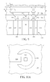
Please refer to FIG. 12. The core column in the composite annular structure 110 is not necessarily a conductive material. The core column may also be an insulting dielectric material column 112. Accordingly, the insulting dielectric material column 112 is surrounded by a first substrate ring 113 or a conductive ring. The first substrate ring 113 or a conductive ring is surrounded by a first dielectric ring 114. The first dielectric ring 114 is surrounded by another substrate ring or a second conductive ring 152. The second conductive ring 152 or a conductive ring is surrounded by a second dielectric ring 117 and the second dielectric ring 117 is surrounded by the substrate in the wafer 103.
Those skilled in the art will readily observe that numerous modifications and alterations of the device and method may be made while retaining the teachings of the invention.

Claims (21)

What is claimed is:
1. A TSV structure comprising:
a wafer comprising a first side and a second side;
a through via connecting said first side and said second side;
a conductive layer filling up said through via;
a through via dielectric ring surrounding and directly contacting said conductive layer;
a first conductive ring surrounding and directly contacting said through via dielectric ring, wherein said first conductive ring and said wafer are of the same material; and
a first dielectric ring surrounding and directly contacting said first conductive ring, and surrounded by said wafer.
2. The TSV structure of claim 1, wherein said conductive layer is electrically connected to a core voltage and said first conductive ring is electrically connected to a first voltage and said core voltage and said first voltage are substantially the same.
3. The TSV structure of claim 1, wherein said conductive layer is electrically connected to a core voltage and said first conductive ring is electrically connected to a first voltage and said core voltage is different from said first voltage.
4. The TSV structure of claim 1, wherein said first conductive ring is for use in shielding the interaction between said conductive layer and said wafer.
5. The TSV structure of claim 1, wherein said conductive layer has a core conductive material and said first conductive ring has a first conductive material and said core conductive material and said first conductive material are substantially the same.
6. The TSV structure of claim 1, wherein said conductive layer has a core conductive material and said first conductive ring has a first conductive material and said core conductive material is different from said first conductive material.
7. The TSV structure of claim 1, further comprising:
a second conductive ring surrounding and directly contacting said first dielectric ring; and
a second dielectric ring surrounding and directly contacting said second conductive ring, and surrounded by said wafer.
8. The TSV structure of claim 1, wherein said conductive layer has a column structure with a diameter of 5 μm-20 μm.
9. The TSV structure of claim 1, further comprising:
a multi-layer metal structure disposed on said first side and comprising a first layer, a second layer and a third layer;
a first conductive ring first extension part composed of said first layer;
a first conductive ring third extension part composed of said third layer; and
a conductive layer second extension part composed of said second layer, wherein said first conductive ring first extension part and said first conductive ring third extension part together sandwich said conductive layer second extension part to shield said conductive layer extension part.
10. The TSV structure of claim 1, wherein said conductive layer second extension part has a serpent-like structure.
11. A method for forming a through-silicon via structure, comprising:
providing a wafer comprising a substrate, a first side and a second side;
forming an composite annular structure in said wafer, wherein said composite annular structure comprises:
a core substrate column;
a through via dielectric ring comprising a dielectric material and surrounding and directly contacting said core substrate column;
a first substrate ring surrounding and directly contacting said through via dielectric ring; and
a first dielectric ring surrounding and directly contacting said first substrate ring, and surrounded by said wafer;
thinning said wafer from the second side to expose said composite annular structure;
forming a second dielectric layer to cover the second side and to expose said composite annular structure;
completely removing said substrate in said core substrate column to form a through via which connects said first side and said second side; and
filling up said through via with a core conductive layer to obtain said through-silicon via structure.
12. The method of claim 11, further comprising
performing a semiconductor procedure after said through-silicon via structure is obtained.
13. The method of claim 11, further comprising
performing a semiconductor procedure before said through-silicon via structure is obtained.
14. The method of claim 11, further comprising
completely removing said first substrate ring to form a first hollow ring; and
filling up said first hollow ring with a first conductive material.
15. The method of claim 14, wherein said core conductive material and said first conductive material are substantially the same.
16. The method of claim 14, wherein said core conductive material is different from said first conductive material.
17. The method of claim 11, further comprising:
forming a second conductive ring surrounding and directly contacting said first dielectric ring; and
forming a second dielectric ring surrounding and directly contacting said second conductive ring, and surrounded by said wafer.
18. The method of claim 11, wherein said conductive layer has a column structure with a diameter of 5 μm-20 μm.
19. The method of claim 11, further comprising:
forming a multi-layer metal structure disposed on said first side and comprising a first layer, a second layer and an third layer;
forming a first conductive ring first extension part composed of said first layer;
forming a first conductive ring third extension part composed of said third layer; and
forming a conductive layer second extension part composed of said second layer.
20. The method of claim 19, wherein said first conductive ring first extension part and said first conductive ring third extension part together sandwich said conductive layer second extension part to shield said conductive layer second extension part.
21. The method of claim 20, wherein said conductive layer second extension part has a zigzag structure.
US13/085,488 2011-04-13 2011-04-13 TSV structure and method for forming the same Active 2031-07-21 US8519515B2 (en)

Priority Applications (1)

Application Number Priority Date Filing Date Title
US13/085,488 US8519515B2 (en) 2011-04-13 2011-04-13 TSV structure and method for forming the same

Applications Claiming Priority (1)

Application Number Priority Date Filing Date Title
US13/085,488 US8519515B2 (en) 2011-04-13 2011-04-13 TSV structure and method for forming the same

Publications (2)

Publication Number Publication Date
US20120261826A1 US20120261826A1 (en) 2012-10-18
US8519515B2 true US8519515B2 (en) 2013-08-27

Family

ID=47005836

Family Applications (1)

Application Number Title Priority Date Filing Date
US13/085,488 Active 2031-07-21 US8519515B2 (en) 2011-04-13 2011-04-13 TSV structure and method for forming the same

Country Status (1)

Country Link
US (1) US8519515B2 (en)

Cited By (7)

* Cited by examiner, † Cited by third party
Publication number Priority date Publication date Assignee Title
US20120049322A1 (en) * 2010-09-01 2012-03-01 Taiwan Semiconductor Manufacturing Company, Ltd. Cylindrical Embedded Capacitors
US20140087548A1 (en) * 2011-07-29 2014-03-27 Taiwan Semiconductor Manufacturing Company, Ltd. Method of shielding through silicon vias in a passive interposer
US8772946B2 (en) * 2012-06-08 2014-07-08 Invensas Corporation Reduced stress TSV and interposer structures
US8916979B2 (en) * 2012-12-28 2014-12-23 Taiwan Semiconductor Manufacturing Company, Ltd. Through-vias and methods of forming the same
US9378778B1 (en) 2015-06-14 2016-06-28 Darryl G. Walker Package including a plurality of stacked semiconductor devices including a capacitance enhanced through via and method of manufacture
US20170040255A1 (en) * 2013-12-23 2017-02-09 Intel Corporation Through-body-via isolated coaxial capacitor and techniques for forming same
US20170250112A1 (en) * 2016-02-26 2017-08-31 Infineon Technologies Ag Semiconductor device and a method for forming a semiconductor device

Families Citing this family (19)

* Cited by examiner, † Cited by third party
Publication number Priority date Publication date Assignee Title
KR101374338B1 (en) * 2007-11-14 2014-03-14 삼성전자주식회사 semicondoctor device having through-via and method of forming the same
US20130015504A1 (en) * 2011-07-11 2013-01-17 Chien-Li Kuo Tsv structure and method for forming the same
US8541883B2 (en) * 2011-11-29 2013-09-24 Advanced Semiconductor Engineering, Inc. Semiconductor device having shielded conductive vias
JP2013115382A (en) * 2011-11-30 2013-06-10 Elpida Memory Inc Semiconductor device and manufacturing method thereof
US8546953B2 (en) 2011-12-13 2013-10-01 Taiwan Semiconductor Manufacturing Co., Ltd. Through silicon via (TSV) isolation structures for noise reduction in 3D integrated circuit
US9275933B2 (en) * 2012-06-19 2016-03-01 United Microelectronics Corp. Semiconductor device
KR101965906B1 (en) * 2012-07-12 2019-04-04 에스케이하이닉스 주식회사 Semiconductor device
US9105701B2 (en) * 2013-06-10 2015-08-11 Micron Technology, Inc. Semiconductor devices having compact footprints
WO2014209330A1 (en) * 2013-06-27 2014-12-31 Intel IP Corporation High conductivity high frequency via for electronic systems
US20150028482A1 (en) * 2013-07-23 2015-01-29 Globalfoundries Inc. Device layout for reducing through-silicon-via stress
US9252077B2 (en) * 2013-09-25 2016-02-02 Intel Corporation Package vias for radio frequency antenna connections
US9793204B2 (en) * 2015-11-17 2017-10-17 Taiwan Semiconductor Manufacturing Company Limited Method of manufacturing semiconductor structure comprising plurality of through holes using metal hard mask
US10607885B2 (en) * 2016-03-30 2020-03-31 Intel Corporation Shell structure for insulation of a through-substrate interconnect
DE102016219275B3 (en) 2016-10-05 2017-08-10 Ihp Gmbh - Innovations For High Performance Microelectronics / Leibniz-Institut Für Innovative Mikroelektronik Technological method for the prevention of vertical / lateral inhomogeneities in the etching of silicon vias by means of buried etch stop layers
US9974201B1 (en) * 2016-10-28 2018-05-15 General Electric Company High power feedthrough for use with a high frequency power converter
US11495559B2 (en) * 2020-04-27 2022-11-08 Taiwan Semiconductor Manufacturing Company, Ltd. Integrated circuits
US20220005747A1 (en) * 2020-07-06 2022-01-06 Changxin Memory Technologies, Inc. Semiconductor structure
CN112397444A (en) * 2020-11-16 2021-02-23 西安电子科技大学 Low-crosstalk silicon through hole structure and manufacturing method thereof
CN114566478B (en) * 2022-04-28 2022-08-05 武汉大学 Coaxial double-ring TSV structure with low thermal stress and high electrical property and preparation method

Citations (32)

* Cited by examiner, † Cited by third party
Publication number Priority date Publication date Assignee Title
US5229647A (en) 1991-03-27 1993-07-20 Micron Technology, Inc. High density data storage using stacked wafers
US5399898A (en) 1992-07-17 1995-03-21 Lsi Logic Corporation Multi-chip semiconductor arrangements using flip chip dies
US5463246A (en) 1988-12-29 1995-10-31 Sharp Kabushiki Kaisha Large scale high density semiconductor apparatus
US5484073A (en) 1994-03-28 1996-01-16 I/O Sensors, Inc. Method for fabricating suspension members for micromachined sensors
US20020017399A1 (en) * 2000-08-11 2002-02-14 Huey-Ru Chang Coaxial via hole and process of fabricating the same
US6407002B1 (en) 2000-08-10 2002-06-18 Taiwan Semiconductor Manufacturing Company Partial resist free approach in contact etch to improve W-filling
US6548891B2 (en) 2000-10-24 2003-04-15 Shinko Electric Industries Co., Ltd. Semiconductor device and production process thereof
US6627985B2 (en) 2001-12-05 2003-09-30 Arbor Company Llp Reconfigurable processor module comprising hybrid stacked integrated circuit die elements
US20040080041A1 (en) 2002-10-21 2004-04-29 Nec Electronics Corporation Semiconductor device with improved heatsink structure
US6800930B2 (en) 2002-07-31 2004-10-05 Micron Technology, Inc. Semiconductor dice having back side redistribution layer accessed using through-silicon vias, and assemblies
US6924551B2 (en) 2003-05-28 2005-08-02 Intel Corporation Through silicon via, folded flex microelectronic package
US7034401B2 (en) 2003-12-17 2006-04-25 Tru-Si Technologies, Inc. Packaging substrates for integrated circuits and soldering methods
US7033934B2 (en) * 2001-11-07 2006-04-25 Shinko Electric Industries Co., Ltd. Method of production of semiconductor package
US20070126085A1 (en) 2005-12-02 2007-06-07 Nec Electronics Corporation Semiconductor device and method of manufacturing the same
US20070161235A1 (en) * 2005-06-14 2007-07-12 John Trezza Back-to-front via process
US20070190692A1 (en) 2006-01-13 2007-08-16 Mete Erturk Low resistance and inductance backside through vias and methods of fabricating same
US7282951B2 (en) 2001-12-05 2007-10-16 Arbor Company Llp Reconfigurable processor module comprising hybrid stacked integrated circuit die elements
US20080073747A1 (en) 2006-09-22 2008-03-27 Clinton Chao Electromagnetic shielding using through-silicon vias
US20080079131A1 (en) * 2006-09-30 2008-04-03 Sung Min Kim Stack package and method for manufacturing the same
US7432592B2 (en) 2005-10-13 2008-10-07 Intel Corporation Integrated micro-channels for 3D through silicon architectures
US7531415B2 (en) 2000-11-30 2009-05-12 Texas Instruments Incorporated Multilayered CMP stop for flat planarization
US20090134498A1 (en) 2007-11-20 2009-05-28 Elpida Memory, Inc. Semiconductor apparatus
US20090189256A1 (en) * 2008-01-29 2009-07-30 Yasuhiro Yoshimura Manufacturing process of semiconductor device and semiconductor device
US20100072579A1 (en) * 2008-09-23 2010-03-25 Andreas Thies Through Substrate Conductors
US20100140749A1 (en) 2008-12-08 2010-06-10 Chien-Li Kuo Semiconductor device
US20100224965A1 (en) * 2009-03-09 2010-09-09 Chien-Li Kuo Through-silicon via structure and method for making the same
US7932584B2 (en) * 2005-06-14 2011-04-26 Cufer Asset Ltd. L.L.C. Stacked chip-based system and method
US7964972B2 (en) * 2004-06-30 2011-06-21 Renesas Electronics Corporation Semiconductor device providing a first electrical conductor and a second electrical conductor in one through hole and method for manufacturing the same
US20110171829A1 (en) * 2007-12-04 2011-07-14 Advanced Semiconductor Engineering, Inc. Method for Forming a Via in a Substrate and Substrate with a Via
US8148824B2 (en) * 2010-04-16 2012-04-03 Nanya Technology Corp. Semiconductor device with through substrate via
US20120112324A1 (en) * 2005-05-18 2012-05-10 Kolo Technologies, Inc. Through-wafer interconnection
US8384207B2 (en) * 2005-08-26 2013-02-26 Honda Motor Co., Ltd. Semiconductor integrated circuit device having insulated through wires

Patent Citations (36)

* Cited by examiner, † Cited by third party
Publication number Priority date Publication date Assignee Title
US5463246A (en) 1988-12-29 1995-10-31 Sharp Kabushiki Kaisha Large scale high density semiconductor apparatus
US5229647A (en) 1991-03-27 1993-07-20 Micron Technology, Inc. High density data storage using stacked wafers
US5399898A (en) 1992-07-17 1995-03-21 Lsi Logic Corporation Multi-chip semiconductor arrangements using flip chip dies
US5484073A (en) 1994-03-28 1996-01-16 I/O Sensors, Inc. Method for fabricating suspension members for micromachined sensors
US6407002B1 (en) 2000-08-10 2002-06-18 Taiwan Semiconductor Manufacturing Company Partial resist free approach in contact etch to improve W-filling
US20020017399A1 (en) * 2000-08-11 2002-02-14 Huey-Ru Chang Coaxial via hole and process of fabricating the same
US6548891B2 (en) 2000-10-24 2003-04-15 Shinko Electric Industries Co., Ltd. Semiconductor device and production process thereof
US7531415B2 (en) 2000-11-30 2009-05-12 Texas Instruments Incorporated Multilayered CMP stop for flat planarization
US7033934B2 (en) * 2001-11-07 2006-04-25 Shinko Electric Industries Co., Ltd. Method of production of semiconductor package
US7282951B2 (en) 2001-12-05 2007-10-16 Arbor Company Llp Reconfigurable processor module comprising hybrid stacked integrated circuit die elements
US6627985B2 (en) 2001-12-05 2003-09-30 Arbor Company Llp Reconfigurable processor module comprising hybrid stacked integrated circuit die elements
US6800930B2 (en) 2002-07-31 2004-10-05 Micron Technology, Inc. Semiconductor dice having back side redistribution layer accessed using through-silicon vias, and assemblies
US20040080041A1 (en) 2002-10-21 2004-04-29 Nec Electronics Corporation Semiconductor device with improved heatsink structure
US6924551B2 (en) 2003-05-28 2005-08-02 Intel Corporation Through silicon via, folded flex microelectronic package
US7034401B2 (en) 2003-12-17 2006-04-25 Tru-Si Technologies, Inc. Packaging substrates for integrated circuits and soldering methods
US20110210426A1 (en) * 2004-06-30 2011-09-01 Renesas Electronics Corporation Semiconductor device providing a first electrical conductor and a second electrical conductor in one through hole and method for manufacturing the same
US7964972B2 (en) * 2004-06-30 2011-06-21 Renesas Electronics Corporation Semiconductor device providing a first electrical conductor and a second electrical conductor in one through hole and method for manufacturing the same
US20120112324A1 (en) * 2005-05-18 2012-05-10 Kolo Technologies, Inc. Through-wafer interconnection
US7932584B2 (en) * 2005-06-14 2011-04-26 Cufer Asset Ltd. L.L.C. Stacked chip-based system and method
US20070161235A1 (en) * 2005-06-14 2007-07-12 John Trezza Back-to-front via process
US8384207B2 (en) * 2005-08-26 2013-02-26 Honda Motor Co., Ltd. Semiconductor integrated circuit device having insulated through wires
US7432592B2 (en) 2005-10-13 2008-10-07 Intel Corporation Integrated micro-channels for 3D through silicon architectures
US20070126085A1 (en) 2005-12-02 2007-06-07 Nec Electronics Corporation Semiconductor device and method of manufacturing the same
US20070190692A1 (en) 2006-01-13 2007-08-16 Mete Erturk Low resistance and inductance backside through vias and methods of fabricating same
US20080073747A1 (en) 2006-09-22 2008-03-27 Clinton Chao Electromagnetic shielding using through-silicon vias
US7525186B2 (en) * 2006-09-30 2009-04-28 Hynix Semiconductor Inc. Stack package having guard ring which insulates through-via interconnection plug and method for manufacturing the same
US20080079131A1 (en) * 2006-09-30 2008-04-03 Sung Min Kim Stack package and method for manufacturing the same
US20090134498A1 (en) 2007-11-20 2009-05-28 Elpida Memory, Inc. Semiconductor apparatus
US20110171829A1 (en) * 2007-12-04 2011-07-14 Advanced Semiconductor Engineering, Inc. Method for Forming a Via in a Substrate and Substrate with a Via
US20090189256A1 (en) * 2008-01-29 2009-07-30 Yasuhiro Yoshimura Manufacturing process of semiconductor device and semiconductor device
US20100072579A1 (en) * 2008-09-23 2010-03-25 Andreas Thies Through Substrate Conductors
US20100140749A1 (en) 2008-12-08 2010-06-10 Chien-Li Kuo Semiconductor device
US20100224965A1 (en) * 2009-03-09 2010-09-09 Chien-Li Kuo Through-silicon via structure and method for making the same
US8168533B2 (en) * 2009-03-09 2012-05-01 United Microelectronics Corp. Through-silicon via structure and method for making the same
US8148824B2 (en) * 2010-04-16 2012-04-03 Nanya Technology Corp. Semiconductor device with through substrate via
US8202801B1 (en) * 2010-04-16 2012-06-19 Nanya Technology Corp. Method of fabricating a semiconductor device with through substrate via

Cited By (18)

* Cited by examiner, † Cited by third party
Publication number Priority date Publication date Assignee Title
US8693163B2 (en) * 2010-09-01 2014-04-08 Taiwan Semiconductor Manufacturing Company, Ltd. Cylindrical embedded capacitors
US9691840B2 (en) 2010-09-01 2017-06-27 Taiwan Semiconductor Manufacturing Company, Ltd. Cylindrical embedded capacitors
US20120049322A1 (en) * 2010-09-01 2012-03-01 Taiwan Semiconductor Manufacturing Company, Ltd. Cylindrical Embedded Capacitors
US9159564B2 (en) * 2011-07-29 2015-10-13 Taiwan Semiconductor Manufacturing Company, Ltd. Method of shielding through silicon vias in a passive interposer
US20140087548A1 (en) * 2011-07-29 2014-03-27 Taiwan Semiconductor Manufacturing Company, Ltd. Method of shielding through silicon vias in a passive interposer
US8772946B2 (en) * 2012-06-08 2014-07-08 Invensas Corporation Reduced stress TSV and interposer structures
US9000600B2 (en) 2012-06-08 2015-04-07 Invensas Corporation Reduced stress TSV and interposer structures
US9349669B2 (en) 2012-06-08 2016-05-24 Invensas Corporation Reduced stress TSV and interposer structures
US8916979B2 (en) * 2012-12-28 2014-12-23 Taiwan Semiconductor Manufacturing Company, Ltd. Through-vias and methods of forming the same
US11682583B2 (en) 2012-12-28 2023-06-20 Taiwan Semiconductor Manufacturing Company, Ltd. Through-vias and methods of forming the same
US10157791B2 (en) 2012-12-28 2018-12-18 Taiwan Semiconductor Manufacturing Company, Ltd. Through-vias and methods of forming the same
US20170040255A1 (en) * 2013-12-23 2017-02-09 Intel Corporation Through-body-via isolated coaxial capacitor and techniques for forming same
US9911689B2 (en) * 2013-12-23 2018-03-06 Intel Corporation Through-body-via isolated coaxial capacitor and techniques for forming same
TWI662685B (en) * 2013-12-23 2019-06-11 英特爾股份有限公司 Through-body-via isolated coaxial capacitor and techniques for forming same
US9378778B1 (en) 2015-06-14 2016-06-28 Darryl G. Walker Package including a plurality of stacked semiconductor devices including a capacitance enhanced through via and method of manufacture
US9455189B1 (en) * 2015-06-14 2016-09-27 Darryl G. Walker Package including a plurality of stacked semiconductor devices including a capacitance enhanced through via and method of manufacture
US9875934B2 (en) * 2016-02-26 2018-01-23 Infineon Technologies Ag Semiconductor device and a method for forming a semiconductor device
US20170250112A1 (en) * 2016-02-26 2017-08-31 Infineon Technologies Ag Semiconductor device and a method for forming a semiconductor device

Also Published As

Publication number Publication date
US20120261826A1 (en) 2012-10-18

Similar Documents

Publication Publication Date Title
US8519515B2 (en) TSV structure and method for forming the same
US8168533B2 (en) Through-silicon via structure and method for making the same
US10431546B2 (en) Manufacturing method for semiconductor device and semiconductor device
TWI503981B (en) Through-substrate vias and methods for forming the same
US8202766B2 (en) Method for fabricating through-silicon via structure
US9646930B2 (en) Semiconductor device having through-substrate vias
US20130015504A1 (en) Tsv structure and method for forming the same
TWI525776B (en) Optimized annular copper tsv
US7846837B2 (en) Through substrate via process
US8421238B2 (en) Stacked semiconductor device with through via
US8481425B2 (en) Method for fabricating through-silicon via structure
TWI732269B (en) Pad structure for enhanced bondability and method of forming the same
US20120276736A1 (en) Method for manufacturing semiconductor device
US20130140688A1 (en) Through Silicon Via and Method of Manufacturing the Same
US8822336B2 (en) Through-silicon via forming method
TWI518861B (en) Tsv structure and method for forming the same
TWI546866B (en) Semiconductor device and fabricating method thereof
US9287173B2 (en) Through silicon via and process thereof
TWI447881B (en) Through-silicon via structure and method for making the same
TWI502716B (en) Method for fabricating through-silicon via structure

Legal Events

Date Code Title Description
AS Assignment

Owner name: UNITED MICROELECTRONICS CORP., TAIWAN

Free format text: ASSIGNMENT OF ASSIGNORS INTEREST;ASSIGNORS:KUO, CHIEN-LI;LIN, CHIA-FANG;REEL/FRAME:026112/0425

Effective date: 20110401

STCF Information on status: patent grant

Free format text: PATENTED CASE

CC Certificate of correction
FPAY Fee payment

Year of fee payment: 4

MAFP Maintenance fee payment

Free format text: PAYMENT OF MAINTENANCE FEE, 8TH YEAR, LARGE ENTITY (ORIGINAL EVENT CODE: M1552); ENTITY STATUS OF PATENT OWNER: LARGE ENTITY

Year of fee payment: 8

AS Assignment

Owner name: MARLIN SEMICONDUCTOR LIMITED, IRELAND

Free format text: ASSIGNMENT OF ASSIGNORS INTEREST;ASSIGNOR:UNITED MICROELECTRONICS CORPORATION;REEL/FRAME:056991/0292

Effective date: 20210618