US8552515B2 - Method for fabricating a damascene self-aligned ferroelectric random access memory (F-RAM) device structure employing reduced processing steps - Google Patents
Method for fabricating a damascene self-aligned ferroelectric random access memory (F-RAM) device structure employing reduced processing steps Download PDFInfo
- Publication number
- US8552515B2 US8552515B2 US13/569,735 US201213569735A US8552515B2 US 8552515 B2 US8552515 B2 US 8552515B2 US 201213569735 A US201213569735 A US 201213569735A US 8552515 B2 US8552515 B2 US 8552515B2
- Authority
- US
- United States
- Prior art keywords
- layer
- forming
- spacers
- depositing
- bottom electrode
- Prior art date
- Legal status (The legal status is an assumption and is not a legal conclusion. Google has not performed a legal analysis and makes no representation as to the accuracy of the status listed.)
- Active
Links
- 238000000034 method Methods 0.000 title claims abstract description 116
- 230000002829 reductive effect Effects 0.000 title abstract description 5
- 238000005530 etching Methods 0.000 claims abstract description 42
- 125000006850 spacer group Chemical group 0.000 claims description 96
- 239000000463 material Substances 0.000 claims description 82
- 238000000151 deposition Methods 0.000 claims description 61
- 229920002120 photoresistant polymer Polymers 0.000 claims description 53
- 238000005229 chemical vapour deposition Methods 0.000 claims description 43
- UQZIWOQVLUASCR-UHFFFAOYSA-N alumane;titanium Chemical compound [AlH3].[Ti] UQZIWOQVLUASCR-UHFFFAOYSA-N 0.000 claims description 41
- 239000000758 substrate Substances 0.000 claims description 38
- 239000010936 titanium Substances 0.000 claims description 31
- PNEYBMLMFCGWSK-UHFFFAOYSA-N aluminium oxide Inorganic materials [O-2].[O-2].[O-2].[Al+3].[Al+3] PNEYBMLMFCGWSK-UHFFFAOYSA-N 0.000 claims description 20
- 229910052593 corundum Inorganic materials 0.000 claims description 20
- TWNQGVIAIRXVLR-UHFFFAOYSA-N oxo(oxoalumanyloxy)alumane Chemical compound O=[Al]O[Al]=O TWNQGVIAIRXVLR-UHFFFAOYSA-N 0.000 claims description 20
- 229910001845 yogo sapphire Inorganic materials 0.000 claims description 20
- 229910052697 platinum Inorganic materials 0.000 claims description 19
- 239000003990 capacitor Substances 0.000 claims description 18
- 230000008569 process Effects 0.000 claims description 15
- 150000004767 nitrides Chemical class 0.000 claims description 14
- 230000008021 deposition Effects 0.000 claims description 13
- 239000003989 dielectric material Substances 0.000 claims description 12
- 239000007772 electrode material Substances 0.000 claims description 11
- 239000004065 semiconductor Substances 0.000 claims description 11
- 229910000510 noble metal Inorganic materials 0.000 claims description 10
- 229910052763 palladium Inorganic materials 0.000 claims description 5
- 239000000126 substance Substances 0.000 claims description 4
- 150000002500 ions Chemical class 0.000 claims description 3
- 238000005498 polishing Methods 0.000 claims description 2
- 229910002673 PdOx Inorganic materials 0.000 claims 4
- 229910019897 RuOx Inorganic materials 0.000 claims 4
- VRIVJOXICYMTAG-IYEMJOQQSA-L iron(ii) gluconate Chemical compound [Fe+2].OC[C@@H](O)[C@@H](O)[C@H](O)[C@@H](O)C([O-])=O.OC[C@@H](O)[C@@H](O)[C@H](O)[C@@H](O)C([O-])=O VRIVJOXICYMTAG-IYEMJOQQSA-L 0.000 claims 4
- 238000000137 annealing Methods 0.000 claims 2
- 238000007517 polishing process Methods 0.000 claims 1
- BASFCYQUMIYNBI-UHFFFAOYSA-N platinum Chemical group [Pt] BASFCYQUMIYNBI-UHFFFAOYSA-N 0.000 description 48
- NRTOMJZYCJJWKI-UHFFFAOYSA-N Titanium nitride Chemical compound [Ti]#N NRTOMJZYCJJWKI-UHFFFAOYSA-N 0.000 description 40
- HFGPZNIAWCZYJU-UHFFFAOYSA-N lead zirconate titanate Chemical compound [O-2].[O-2].[O-2].[O-2].[O-2].[Ti+4].[Zr+4].[Pb+2] HFGPZNIAWCZYJU-UHFFFAOYSA-N 0.000 description 29
- HQVNEWCFYHHQES-UHFFFAOYSA-N silicon nitride Chemical compound N12[Si]34N5[Si]62N3[Si]51N64 HQVNEWCFYHHQES-UHFFFAOYSA-N 0.000 description 11
- 238000004519 manufacturing process Methods 0.000 description 8
- 239000001257 hydrogen Substances 0.000 description 7
- 229910052739 hydrogen Inorganic materials 0.000 description 7
- WFKWXMTUELFFGS-UHFFFAOYSA-N tungsten Chemical compound [W] WFKWXMTUELFFGS-UHFFFAOYSA-N 0.000 description 7
- UFHFLCQGNIYNRP-UHFFFAOYSA-N Hydrogen Chemical compound [H][H] UFHFLCQGNIYNRP-UHFFFAOYSA-N 0.000 description 6
- 229910052581 Si3N4 Inorganic materials 0.000 description 5
- QVGXLLKOCUKJST-UHFFFAOYSA-N atomic oxygen Chemical compound [O] QVGXLLKOCUKJST-UHFFFAOYSA-N 0.000 description 5
- 239000007789 gas Substances 0.000 description 5
- 239000001301 oxygen Substances 0.000 description 5
- 229910052760 oxygen Inorganic materials 0.000 description 5
- 238000003860 storage Methods 0.000 description 5
- 229910052721 tungsten Inorganic materials 0.000 description 5
- 239000010937 tungsten Substances 0.000 description 5
- RTAQQCXQSZGOHL-UHFFFAOYSA-N Titanium Chemical compound [Ti] RTAQQCXQSZGOHL-UHFFFAOYSA-N 0.000 description 4
- 229910052454 barium strontium titanate Inorganic materials 0.000 description 4
- 239000005380 borophosphosilicate glass Substances 0.000 description 4
- 230000015654 memory Effects 0.000 description 4
- KDLHZDBZIXYQEI-UHFFFAOYSA-N Palladium Chemical compound [Pd] KDLHZDBZIXYQEI-UHFFFAOYSA-N 0.000 description 3
- 125000004429 atom Chemical group 0.000 description 3
- 230000004888 barrier function Effects 0.000 description 3
- 230000015572 biosynthetic process Effects 0.000 description 3
- 238000005538 encapsulation Methods 0.000 description 3
- 230000006870 function Effects 0.000 description 3
- 230000004048 modification Effects 0.000 description 3
- 238000012986 modification Methods 0.000 description 3
- -1 platinum titanium aluminum Chemical compound 0.000 description 3
- 230000010287 polarization Effects 0.000 description 3
- 229910052719 titanium Inorganic materials 0.000 description 3
- XKRFYHLGVUSROY-UHFFFAOYSA-N Argon Chemical compound [Ar] XKRFYHLGVUSROY-UHFFFAOYSA-N 0.000 description 2
- VNSWULZVUKFJHK-UHFFFAOYSA-N [Sr].[Bi] Chemical compound [Sr].[Bi] VNSWULZVUKFJHK-UHFFFAOYSA-N 0.000 description 2
- 230000015556 catabolic process Effects 0.000 description 2
- 239000003795 chemical substances by application Substances 0.000 description 2
- 238000006731 degradation reaction Methods 0.000 description 2
- HTXDPTMKBJXEOW-UHFFFAOYSA-N dioxoiridium Chemical compound O=[Ir]=O HTXDPTMKBJXEOW-UHFFFAOYSA-N 0.000 description 2
- 230000005684 electric field Effects 0.000 description 2
- 238000005516 engineering process Methods 0.000 description 2
- 238000010438 heat treatment Methods 0.000 description 2
- 229910000457 iridium oxide Inorganic materials 0.000 description 2
- HBEQXAKJSGXAIQ-UHFFFAOYSA-N oxopalladium Chemical compound [Pd]=O HBEQXAKJSGXAIQ-UHFFFAOYSA-N 0.000 description 2
- 229910003445 palladium oxide Inorganic materials 0.000 description 2
- 239000010948 rhodium Substances 0.000 description 2
- 229910003450 rhodium oxide Inorganic materials 0.000 description 2
- 229910001925 ruthenium oxide Inorganic materials 0.000 description 2
- WOCIAKWEIIZHES-UHFFFAOYSA-N ruthenium(iv) oxide Chemical compound O=[Ru]=O WOCIAKWEIIZHES-UHFFFAOYSA-N 0.000 description 2
- XJDNKRIXUMDJCW-UHFFFAOYSA-J titanium tetrachloride Chemical compound Cl[Ti](Cl)(Cl)Cl XJDNKRIXUMDJCW-UHFFFAOYSA-J 0.000 description 2
- QGZKDVFQNNGYKY-UHFFFAOYSA-N Ammonia Chemical compound N QGZKDVFQNNGYKY-UHFFFAOYSA-N 0.000 description 1
- 229910015844 BCl3 Inorganic materials 0.000 description 1
- OYPRJOBELJOOCE-UHFFFAOYSA-N Calcium Chemical compound [Ca] OYPRJOBELJOOCE-UHFFFAOYSA-N 0.000 description 1
- KZBUYRJDOAKODT-UHFFFAOYSA-N Chlorine Chemical compound ClCl KZBUYRJDOAKODT-UHFFFAOYSA-N 0.000 description 1
- ZAMOUSCENKQFHK-UHFFFAOYSA-N Chlorine atom Chemical compound [Cl] ZAMOUSCENKQFHK-UHFFFAOYSA-N 0.000 description 1
- KJTLSVCANCCWHF-UHFFFAOYSA-N Ruthenium Chemical compound [Ru] KJTLSVCANCCWHF-UHFFFAOYSA-N 0.000 description 1
- MXSJNBRAMXILSE-UHFFFAOYSA-N [Si].[P].[B] Chemical compound [Si].[P].[B] MXSJNBRAMXILSE-UHFFFAOYSA-N 0.000 description 1
- 229910000086 alane Inorganic materials 0.000 description 1
- AZDRQVAHHNSJOQ-UHFFFAOYSA-N alumane Chemical compound [AlH3] AZDRQVAHHNSJOQ-UHFFFAOYSA-N 0.000 description 1
- 229910052786 argon Inorganic materials 0.000 description 1
- 229910052791 calcium Inorganic materials 0.000 description 1
- 239000011575 calcium Substances 0.000 description 1
- 239000003153 chemical reaction reagent Substances 0.000 description 1
- 239000000460 chlorine Substances 0.000 description 1
- 229910052801 chlorine Inorganic materials 0.000 description 1
- 239000011248 coating agent Substances 0.000 description 1
- 238000000576 coating method Methods 0.000 description 1
- 230000002860 competitive effect Effects 0.000 description 1
- 230000000295 complement effect Effects 0.000 description 1
- 150000001875 compounds Chemical class 0.000 description 1
- 238000010276 construction Methods 0.000 description 1
- 239000013078 crystal Substances 0.000 description 1
- 238000013500 data storage Methods 0.000 description 1
- 238000005137 deposition process Methods 0.000 description 1
- 230000000694 effects Effects 0.000 description 1
- 239000011521 glass Substances 0.000 description 1
- 150000002431 hydrogen Chemical class 0.000 description 1
- 238000003384 imaging method Methods 0.000 description 1
- 229910052741 iridium Inorganic materials 0.000 description 1
- GKOZUEZYRPOHIO-UHFFFAOYSA-N iridium atom Chemical compound [Ir] GKOZUEZYRPOHIO-UHFFFAOYSA-N 0.000 description 1
- 229910052746 lanthanum Inorganic materials 0.000 description 1
- FZLIPJUXYLNCLC-UHFFFAOYSA-N lanthanum atom Chemical group [La] FZLIPJUXYLNCLC-UHFFFAOYSA-N 0.000 description 1
- 230000014759 maintenance of location Effects 0.000 description 1
- 230000000873 masking effect Effects 0.000 description 1
- 229910052751 metal Inorganic materials 0.000 description 1
- 239000002184 metal Substances 0.000 description 1
- 229910044991 metal oxide Inorganic materials 0.000 description 1
- 150000004706 metal oxides Chemical class 0.000 description 1
- 238000001465 metallisation Methods 0.000 description 1
- DAZXVJBJRMWXJP-UHFFFAOYSA-N n,n-dimethylethylamine Chemical compound CCN(C)C DAZXVJBJRMWXJP-UHFFFAOYSA-N 0.000 description 1
- SJLOMQIUPFZJAN-UHFFFAOYSA-N oxorhodium Chemical compound [Rh]=O SJLOMQIUPFZJAN-UHFFFAOYSA-N 0.000 description 1
- 230000036961 partial effect Effects 0.000 description 1
- 238000001020 plasma etching Methods 0.000 description 1
- 150000003057 platinum Chemical class 0.000 description 1
- 230000004044 response Effects 0.000 description 1
- 229910052703 rhodium Inorganic materials 0.000 description 1
- MHOVAHRLVXNVSD-UHFFFAOYSA-N rhodium atom Chemical compound [Rh] MHOVAHRLVXNVSD-UHFFFAOYSA-N 0.000 description 1
- 229910052707 ruthenium Inorganic materials 0.000 description 1
- VSZWPYCFIRKVQL-UHFFFAOYSA-N selanylidenegallium;selenium Chemical compound [Se].[Se]=[Ga].[Se]=[Ga] VSZWPYCFIRKVQL-UHFFFAOYSA-N 0.000 description 1
- 230000035945 sensitivity Effects 0.000 description 1
- 229910052710 silicon Inorganic materials 0.000 description 1
- 239000010703 silicon Substances 0.000 description 1
- 238000000992 sputter etching Methods 0.000 description 1
- 230000003068 static effect Effects 0.000 description 1
- 229910052712 strontium Inorganic materials 0.000 description 1
- CIOAGBVUUVVLOB-UHFFFAOYSA-N strontium atom Chemical compound [Sr] CIOAGBVUUVVLOB-UHFFFAOYSA-N 0.000 description 1
- VEALVRVVWBQVSL-UHFFFAOYSA-N strontium titanate Chemical compound [Sr+2].[O-][Ti]([O-])=O VEALVRVVWBQVSL-UHFFFAOYSA-N 0.000 description 1
- FAQYAMRNWDIXMY-UHFFFAOYSA-N trichloroborane Chemical compound ClB(Cl)Cl FAQYAMRNWDIXMY-UHFFFAOYSA-N 0.000 description 1
Images


Classifications
-
- H—ELECTRICITY
- H10—SEMICONDUCTOR DEVICES; ELECTRIC SOLID-STATE DEVICES NOT OTHERWISE PROVIDED FOR
- H10N—ELECTRIC SOLID-STATE DEVICES NOT OTHERWISE PROVIDED FOR
- H10N52/00—Hall-effect devices
- H10N52/01—Manufacture or treatment
-
- H—ELECTRICITY
- H01—ELECTRIC ELEMENTS
- H01L—SEMICONDUCTOR DEVICES NOT COVERED BY CLASS H10
- H01L28/00—Passive two-terminal components without a potential-jump or surface barrier for integrated circuits; Details thereof; Multistep manufacturing processes therefor
- H01L28/40—Capacitors
- H01L28/55—Capacitors with a dielectric comprising a perovskite structure material
-
- H—ELECTRICITY
- H01—ELECTRIC ELEMENTS
- H01L—SEMICONDUCTOR DEVICES NOT COVERED BY CLASS H10
- H01L28/00—Passive two-terminal components without a potential-jump or surface barrier for integrated circuits; Details thereof; Multistep manufacturing processes therefor
- H01L28/40—Capacitors
- H01L28/60—Electrodes
- H01L28/75—Electrodes comprising two or more layers, e.g. comprising a barrier layer and a metal layer
-
- H—ELECTRICITY
- H10—SEMICONDUCTOR DEVICES; ELECTRIC SOLID-STATE DEVICES NOT OTHERWISE PROVIDED FOR
- H10B—ELECTRONIC MEMORY DEVICES
- H10B53/00—Ferroelectric RAM [FeRAM] devices comprising ferroelectric memory capacitors
- H10B53/30—Ferroelectric RAM [FeRAM] devices comprising ferroelectric memory capacitors characterised by the memory core region
-
- H—ELECTRICITY
- H01—ELECTRIC ELEMENTS
- H01L—SEMICONDUCTOR DEVICES NOT COVERED BY CLASS H10
- H01L29/00—Semiconductor devices adapted for rectifying, amplifying, oscillating or switching, or capacitors or resistors with at least one potential-jump barrier or surface barrier, e.g. PN junction depletion layer or carrier concentration layer; Details of semiconductor bodies or of electrodes thereof ; Multistep manufacturing processes therefor
- H01L29/40—Electrodes ; Multistep manufacturing processes therefor
- H01L29/401—Multistep manufacturing processes
- H01L29/4011—Multistep manufacturing processes for data storage electrodes
- H01L29/40111—Multistep manufacturing processes for data storage electrodes the electrodes comprising a layer which is used for its ferroelectric properties
-
- H—ELECTRICITY
- H01—ELECTRIC ELEMENTS
- H01L—SEMICONDUCTOR DEVICES NOT COVERED BY CLASS H10
- H01L29/00—Semiconductor devices adapted for rectifying, amplifying, oscillating or switching, or capacitors or resistors with at least one potential-jump barrier or surface barrier, e.g. PN junction depletion layer or carrier concentration layer; Details of semiconductor bodies or of electrodes thereof ; Multistep manufacturing processes therefor
- H01L29/40—Electrodes ; Multistep manufacturing processes therefor
- H01L29/43—Electrodes ; Multistep manufacturing processes therefor characterised by the materials of which they are formed
- H01L29/49—Metal-insulator-semiconductor electrodes, e.g. gates of MOSFET
- H01L29/51—Insulating materials associated therewith
- H01L29/516—Insulating materials associated therewith with at least one ferroelectric layer
-
- H—ELECTRICITY
- H10—SEMICONDUCTOR DEVICES; ELECTRIC SOLID-STATE DEVICES NOT OTHERWISE PROVIDED FOR
- H10B—ELECTRONIC MEMORY DEVICES
- H10B53/00—Ferroelectric RAM [FeRAM] devices comprising ferroelectric memory capacitors
Definitions
- the present invention relates, in general, to the field of integrated circuit (IC) memory devices. More particularly, the present invention relates to the field of non-volatile, ferroelectric random access memory (F-RAM) devices and a method for fabricating a damascene self-aligned F-RAM device structure on a planar surface using a reduced number of masks and etching steps.
- IC integrated circuit
- F-RAM ferroelectric random access memory
- WSTS World Semiconductor Trade Statistics
- the semiconductor market reached an important milestone in 2010, posting worldwide revenues of more than $300 billion (in United States dollars) for the first time in the industry's history.
- the memory chip segment exhibited the highest growth rate during 2010, increasing from $45 billion in 2009 to $71 billion in 2010, representing a 57% year-over-year growth rate.
- Embedded memory devices represented more than 23% of the overall semiconductor market in 2010.
- F-RAM has emerged as a promising option for the industry, particularly in the market areas of mobile computing, smart meters, radio frequency identification (RFID) devices, office equipment and other applications requiring non-volatile data storage.
- RFID radio frequency identification
- Standard dynamic random access memory (DRAM) and static random access memory (SRAM) devices while providing relatively fast access times, are considered to be volatile memory devices inasmuch as data stored in such memories is lost when power is interrupted.
- non-volatile memory devices are those that function to retain data despite any loss of power.
- F-RAM devices are inherently non-volatile, meaning that these memory devices are able to retain stored data while the device is not powered.
- EEPROM electrically erasable programmable read only memory
- F-RAM devices have several advantages including lower power requirements (operational voltages of just 5V needed during read-write operations), higher read-write speeds (less than 70 nanoseconds), and virtually unlimited write endurance capability (more than 10,000,000,000 write cycles).
- F-RAM memory devices may be fabricated based on the use of lead zirconium titanate (PZT) ferroelectric storage capacitors as memory elements integrated with complementary metal oxide semiconductor (CMOS) addressing, selection, and control logic.
- PZT lead zirconium titanate
- CMOS complementary metal oxide semiconductor
- PLZT is a lanthanum-doped form of PZT wherein some of the lead is replaced with Lanthanum.
- PZT may also be doped with strontium and calcium to improve its ferroelectric dielectric properties.
- Ferroelectric storage capacitors having a strontium bismuth tantalate (SBT); barium strontium titanate (BST); and strontium titanate oxide (STO) dielectrics are also known in the art.
- PZT shall also be considered to include PLZT, SBT, BST, STO and other comparable ferroelectric dielectric materials.
- the techniques of the present invention disclosed herein are applicable to all known ferroelectric dielectrics including Perovskites and layered Perovskites (whether doped or undoped) including PZT, PLZT, BST, SBT, STO and others while simultaneously allowing for a potentially broader choice of electrode materials and the use of a forming gas anneal process step on the completed IC structure.
- F-RAM devices function through their ability to be polarized in one direction or another in order to store a binary value representative of a logic level “one” or “zero”.
- the ferroelectric effect allows for the retention of a stable polarization state in the absence of an applied electric field due to the alignment of internal dipoles within the Perovskite crystals in the dielectric material. This alignment may be selectively achieved by application of an electric field which exceeds the coercive field of the material. Conversely, reversal of the applied field reverses the internal dipoles.
- a hysteresis curve wherein the abscissa and ordinate represent the applied voltage (“V”) and resulting polarization (“Q”) states respectively, may be plotted to represent the response of the polarization of a ferroelectric capacitor to the applied voltage.
- V applied voltage
- Q resulting polarization
- a more complete description of this characteristic hysteresis curve is disclosed, for example, in U.S. Pat. Nos. 4,914,627 and 4,888,733 assigned to Ramtron International Corporation, assignee of the present invention, the disclosures of which are herein specifically incorporated by this reference.
- F-RAMs currently account for a relatively small share of the non-volatile memory device market.
- the main limitation of the F-RAM technology has been its lower storage density compared to FLASH devices coupled with higher manufacturing costs.
- These limitations stem primarily from the generally complex structure of current F-RAM devices which results in a manufacturing process that requires a high number of processing masks and etching steps.
- F-RAM devices need to be more highly integrated, implying increased storage densities and reduced manufacturing costs.
- a method for forming a damascene self-aligned ferroelectric RAM (F-RAM) device on a planar surface comprising the steps of forming, on a planar surface of a semiconductor substrate, a thick oxide layer which is etched based on the pattern established by a non-erodible mask, forming an opening for the F-RAM construction, followed by the application and etching of a CVD aluminum oxide conformal layer to form spacers, deposition of a titanium aluminum nitride layer, followed by the application and O 2 plasma ash etching of a photoresist material, deposition and planarization of an oxide material using chemical mechanical polishing (CMP), application of a photoresist mask to create an etching pattern on the oxide, deposition of a CVD aluminum oxide conformal layer to form a second set of spacers after the oxide is etched, deposition, planarization and etching of a ferroelectric layer ideally doped with lead zirconium titanate (PZT)
- Also further disclosed herein is a method for forming an integrated circuit device on a substrate comprising forming a first insulating layer on the substrate and removing a portion of the first insulating layer to produce an opening to an exposed surface of the substrate therein.
- First spacers are formed on sidewalls of the opening and a first conductive layer is formed on the exposed surface of the substrate separated from the first spacers on the sidewalls of the opening by a gap therebetween.
- a bottom electrode of a ferroelectric capacitor is formed over the first conductive layer and in the gap laterally of the first conductive layer.
- a second insulating layer is formed adjoining the spacers in the opening and second spacers are formed on the second insulating layer in the opening.
- a ferroelectric dielectric layer is formed on the bottom electrode between the second spacers and a top electrode is formed on the ferroelectric dielectric.
- a bottom electrode contact opening is formed through a portion of the second insulating layer to the bottom electrode and a first electrical contact is formed to the top electrode and a second electrical contact is formed to the bottom electrode through the bottom electrode contact opening.
- Still further disclosed herein is a method for forming a ferroelectric device on a planar surface of a semiconductor substrate comprising forming a relatively thick oxide layer on the planar surface and selectively etching an opening through the oxide layer in a pattern established by a non-erodible mask.
- a first aluminum oxide conformal layer is applied and selectively etched to form first spacers on sidewalls of the opening and a titanium aluminum nitride layer is deposited in a lower portion of the opening and separated from the first spacers.
- a bottom electrode of a ferroelectric capacitor is formed over the aluminum oxide layer in contact with the spacers and laterally of the aluminum oxide layer.
- An oxide material is deposited, planarized and selectively removed to form an additional oxide layer adjoining the first spacers in the opening.
- a second aluminum oxide layer is deposited and selectively etched to form second spacers on the additional oxide layer.
- a ferroelectric layer is deposited and etched on the bottom electrode between the second spacers.
- a top electrode is formed on the ferroelectric layer and a Ti/TiN and W contact is formed to the bottom electrode through the oxide material and a Ti/TiN and W contact is also substantially concurrently formed to the top electrode.
- a ferroelectric device which comprises a contact stud formed upon a semiconductor substrate and a first conductive layer overlying the substrate and adjoining the contact stud.
- a bottom electrode layer overlies the first conductive layer and first spacers are disposed laterally of the bottom electrode layer extending distally of the substrate.
- Second spacers are disposed on the bottom electrode layer extending distally therefrom substantially parallel to the first spacers and an insulating layer is disposed between the first and second spacers.
- a ferroelectric dielectric layer overlies the bottom electrode layer between the second spacers and a top electrode layer overlies the ferroelectric dielectric layer.
- a top electrode contact adjoins the top electrode layer and a bottom electrode contact adjoins the bottom electrode layer extending through the insulating layer.
- Also further disclosed herein is a method for forming an integrated circuit device on a substrate including at least one contact stud.
- the method comprises forming a first insulating layer on the substrate and removing a portion of the first insulating layer to produce an opening to an exposed surface of said substrate therein.
- First spacers are formed on the sidewalls of the opening and a first conductive layer is formed in contact with the contact stud on the exposed surface of the substrate separated from the first spacers on the sidewalls of the opening by a gap therebetween.
- a bottom electrode of a ferroelectric capacitor is formed over the first conductive layer and in the gap laterally of the first conductive layer.
- a second insulating layer is formed adjoining the spacers in the opening and second spacers are formed on the second insulating layer in the opening.
- a ferroelectric dielectric is formed on the bottom electrode between the second spacers and a top electrode is formed on the ferroelectric dielectric. An electrical contact is then formed to the top electrode.
- a ferroelectric device which comprises a semiconductor substrate and a first conductive layer overlying the semiconductor substrate.
- a bottom electrode layer overlies the first conductive layer and first spacers are disposed laterally of the bottom electrode layer and extend distally of the substrate.
- Second spacers are disposed on the bottom electrode layer and extend distally therefrom substantially parallel to the first spacers.
- An insulating layer is disposed between the first and second spacers and a ferroelectric dielectric layer overlies the bottom electrode layer between the second spacers.
- a top electrode layer overlies the ferroelectric dielectric layer, a top electrode contact adjoins the top electrode layer and a bottom electrode contact adjoins the bottom electrode layer extending through the insulating layer.
- FIG. 1 illustrates a partial, cross-sectional view of the structure of an F-RAM substrate providing a depiction of the first-level F-RAM substrate with contact studs;
- FIG. 2 is a follow-on view of the structure of the F-RAM substrate of the preceding figure after a thick oxide layer is deposited;
- FIG. 3 is a follow-on view of the structure of a non-erodible mask
- FIG. 4 is a follow-on view of the structure of the F-RAM opening
- FIG. 5 is a follow-on view of the structure of the F-RAM opening after non-erodible mask is removed;
- FIG. 6 is a follow-on view of the conformal CVD structure
- FIG. 7 is a follow-on view of the F-RAM structure with Al 2 O 3 spacers
- FIG. 8 is a follow-on view of the titanium aluminum nitride structure
- FIG. 9 is a follow-on view of the photoresist application structure
- FIG. 10 is a follow-on view of the etched photoresist structure
- FIG. 11 is a follow-on view of the etched titanium aluminum nitride structure
- FIG. 12 is a follow-on view of the F-RAM titanium aluminum nitride structure
- FIG. 13 is a follow-on view of the F-RAM platinum structure
- FIG. 14 is a follow-on view of the second photoresist application structure
- FIG. 15 is a follow-on view of the etched photoresist structure
- FIG. 16 is a follow-on view of the etched platinum structure
- FIG. 17 is a follow-on view of the F-RAM platinum titanium aluminum nitride structure
- FIG. 18 is a follow-on view of the oxide deposition structure
- FIG. 19 is a follow-on view of the CMP oxide structure
- FIG. 20 is a follow-on view of the photoresist mask structure
- FIG. 21 is a follow-on view of the etched oxide structure
- FIG. 22 is a follow-on view of the second conformal CVD structure
- FIG. 23 is a follow-on view of the F-RAM Al 2 O 3 structure
- FIG. 24 is a follow-on view of the F-RAM PZT structure
- FIG. 25 is a follow-on view of the F-RAM PZT electrode structure
- FIG. 26 is a follow-on view of the F-RAM PZT Ti/TiN structure
- FIG. 27 is a follow-on view of the F-RAM PZT nitride structure
- FIG. 28 is a follow-on view of the contact photoresist mask structure
- FIG. 29 is a follow-on view of the contact oxide etching structure
- FIG. 30 is a follow-on view of the contact nitride etching structure.
- FIG. 31 is a follow-on view of the F-RAM contact stud structure.
- the present invention presents a novel, non-volatile, ferroelectric random access memory (F-RAM) device and a method for fabricating a damascene self-aligned F-RAM device structure on a planar surface using a reduced number of masks and etching steps.
- F-RAM ferroelectric random access memory
- a representative method in accordance with the present invention comprises the processing steps disclosed in FIGS. 1 through 31 inclusive.
- F-RAM substrate 100 provides a depiction of the first-level F-RAM substrate with contact stud 108 and contact stud 110 .
- a layer of BSPG 102 boron phosphorus silicon glass
- BSPG 102 boron phosphorus silicon glass
- Any oxide, nitride, or other appropriate dielectric can be substituted for the BPSG 102 layer.
- contact stud 108 and contact stud 110 are formed by Ti/TiN 104 (titanium/titanium nitride) liners and a chemical vapor deposition (CVD) of CVD tungsten (W) 106 .
- F-RAM substrate 200 depicting a thick oxide 202 layer of one to two microns thick, deposited over the F-RAM substrate 100 .
- the thick oxide 202 layer is planar as it is deposited over the planarized surface, BPSG 102 .
- a photoresist non-erodible mask 300 is shown. Following the process in FIG. 3 , the first contact stud 110 is masked over using a photoresist mask 302 . Masking may be performed through a standard process of spin applying photoresist, imaging it and developing it leaving an opening 303
- an F-RAM opening structure 400 is shown.
- the exposed portion of the thick oxide 202 layer surface is then etched away with a reactive-ion etching process using standard etch gases such as, but not limited, to CF 4 and H 2 in oxygen.
- This etching technique creates the F-RAM opening 402 where the F-RAM will be constructed.
- the BPSG layer 102 may be over etched and recessed (not shown).
- the F-RAM opening structure 500 is shown with the photoresist mask removed from F-RAM opening structure 400 .
- the photoresist mask 302 may be removed employing a standard O 2 plasma ash.
- the conformal CVD structure 600 is shown.
- a layer of between 2000 to 4000 angstroms of CVD aluminum oxide (Al 2 0 3 ) is subsequently deposited over the F-RAM opening structure 500 , forming a conformal CVD 602 layer of aluminum oxide on the top, sides and bottom of the thick oxide 202 layer.
- FIG. 7 the removal of a portion of the CVD Al 2 O 3 material layer to create F-RAM structure with AL 2 O 3 spacers 700 is depicted.
- the conformal CVD 602 layer is removed from the top and bottom using a reactive ion directional etch using Cl 2 /BCl 3 /CCF 4 /Ar on the planar surfaces leaving Al 2 O 3 spacers 702 .
- FIG. 8 the F-RAM structure with AL 2 O 3 spacers 700 is shown with the addition of a conformal layer of about 1000 angstroms of titanium aluminum nitride film by a chemical vapor deposition (CVD) system.
- CVD chemical vapor deposition
- Titanium tetrachloride (TiCl 4 ), dimethylethylamine alane (DMEAA) and ammonia gas may be used as source gases.
- a layer of titanium aluminum nitride 802 is formed over the top of the F-RAM structure with AL 2 O 3 spacers 700 . Note that the titanium aluminum nitride 802 layer covers the sides and bottom of the F-RAM opening 402 .
- FIG. 9 the application of a photoresist material on top of the titanium aluminum nitride structure 800 (titanium aluminum nitride) is shown, forming photoresist application structure 900 .
- a photoresist 902 material is spun applied over the top of the titanium aluminum nitride structure 800 (titanium aluminum nitride).
- the etching of the photoresist material in photoresist application structure 900 is shown to create etched photoresist structure 1000 .
- the photoresist 902 material is etched back using an oxygen (O 2 ) plasma ash in order to shape a structure below the surface of the titanium aluminum nitride 802 layer, leaving the photoresist 902 materials in the F-RAM opening 402 .
- O 2 oxygen
- etched titanium aluminum nitride structure 1100 etched titanium aluminum nitride
- the titanium aluminum nitride is wet etched.
- the titanium aluminum nitride 802 layer is etched away exposing the base of the thick oxide 202 layer and also forming thin etched openings 1102 between the photoresist 902 material and the Al 2 O 3 spacers 702 .
- section 1104 An enhanced view of section 1104 is shown (above-right) to detail the structure formed after the etching away of the titanium aluminum nitride 802 layer.
- Section 1104 illustrates how the titanium aluminum nitride 802 coating is etched back to the base of the thick oxide 202 layer, leaving a layer of titanium aluminum nitride 802 only below the remaining photoresist 902 material.
- the removal of the remainder of the photoresist material in the etched titanium aluminum nitride structure 1100 is shown, forming F-RAM titanium aluminum nitride structure 1200 .
- the photoresist 902 material is completely removed by the same O 2 plasma ash process described above. Note that a titanium aluminum nitride 802 layer remains on the base of the thick oxide 202 in the F-RAM opening 402 .
- a layer of CVD platinum deposited over the top of the F-RAM titanium aluminum nitride structure 1200 is shown, forming F-RAM platinum structure 1300 .
- a conformal platinum 1302 layer of 500 to 1000 angstroms is deposited by chemical vapor deposition over the top of the F-RAM titanium aluminum nitride structure 1200 .
- This platinum 1302 layer covers the top and bottom of the thick oxide 202 , the top of the titanium aluminum nitride 802 layer and sidewalls of the Al 2 O 3 spacers 702 .
- FIG. 14 an application of photoresist material on top of the F-RAM platinum structure 1300 is shown, forming the second photoresist application structure 1400 .
- a photoresist 1402 material is applied for the second time (as in FIG. 9 ) over the top of the F-RAM platinum structure 1300 .
- the removal of a portion of the photoresist material in the second photoresist application structure 1400 is shown, forming etched photoresist structure 1500 .
- the photoresist 1402 material is etched back using an oxygen (O 2 ) plasma ash in order to shape a structure below the surface of the conformal platinum 1302 layer. This etching process leaves the photoresist 1402 material only in the F-RAM opening 402 .
- the removal of a portion of the platinum layer in the etched photoresist structure 1500 is depicted, creating etched platinum structure 1600 .
- the conformal platinum 1302 layer is etched away from the top of the thick oxide 202 and the sides of the Al 2 O 3 spacers 702 , forming a second etched opening 1602 between the photoresist 1402 material and the Al 2 O 3 .
- the platinum 1302 layer is not etched all the way back to base of the thick oxide 202 layer in the F-RAM opening 402 .
- Platinum is typically etched using a wet etch in an argon or chlorine atmosphere, although other gases may be used. Ion milling can be used as well as an alternative etching technique.
- the photoresist 1402 material is left on top of the platinum 1302 layer in the F-RAM opening 402 .
- FIG. 17 the removal of the remainder of the photoresist material from the etched platinum structure 1600 is depicted, creating F-RAM platinum titanium aluminum nitride structure 1700 (titanium aluminum nitride).
- F-RAM platinum titanium aluminum nitride structure 1700 titanium aluminum nitride
- just the photoresist 1402 material is etched away using an O 2 plasma ash etching technique and removed with a vacuum pump. Note that in this process step, the titanium aluminum nitride 802 layer remains at the base of the thick oxide 202 layer, with the platinum 1302 layer positioned above the titanium aluminum nitride 802 layer and is also in contact with the base of the thick oxide 202 layer.
- oxide deposition structure 1800 With reference additionally now to FIG. 18 , the deposition of an oxide layer over the top of the F-RAM platinum titanium aluminum nitride structure 1700 (titanium aluminum nitride) is shown, creating oxide deposition structure 1800 .
- an oxide 1802 layer thick enough to completely fill the F-RAM opening 402 is formed.
- CMP oxide structure 1900 the removal of the oxide material in the oxide deposition structure 1800 is shown to form CMP oxide structure 1900 .
- CMP is used once more to polish away the oxide 1802 material all the way back to the level of the thick oxide 202 to form a planar surface 1902 on top of the thick oxide 202 . Notice that the oxide 1802 remains embedded in F-RAM opening 402 and is planar to the top surface of the thick oxide 202 .
- FIG. 20 the application of a photoresist mask over the CMP oxide structure 1900 is shown, creating photoresist mask structure 2000 .
- a photoresist mask 2002 is deposited over the CMP oxide structure 1900 and then imaged and developed to form a mask opening 2004 . This step leaves the oxide 1802 partially exposed in the area of the F-RAM opening 402 .
- the etching of the exposed oxide in the photoresist mask structure 2000 is shown, forming etched oxide structure 2100 .
- the oxide 1802 material in the F-RAM opening 402 is etched down to the platinum 1302 layer. This oxide 1802 material can be removed using reactive-ion etch processing. This step creates oxide 1802 layers on each side of the F-RAM opening 402 .
- the formation of the second conformal CVD structure 2200 is shown.
- the photoresist mask 2002 is subsequently removed using the same O 2 plasma ash etching technique described above.
- a second layer of 1000 to 2000 angstroms of Al 2 O 3 is then deposited using chemical vapor deposition (as in FIG. 6 ) over the top of the thick oxide 202 , the etched oxide 1802 , the platinum 1302 and the sides and bottom of the F-RAM opening 402 , forming a another conformal CVD oxide 2202 layer of Al 2 O 3 .
- the removal of a portion of the conformal CVD layer from the second conformal CVD structure 2200 is shown, forming an F-RAM Al 2 O 3 structure 2300 .
- the conformal CVD oxide 2202 layer is etched away from the planar regions of the thick oxide 202 with a directional reactive-ion etch, forming the second set of Al 2 O 3 spacers 2302 . Note that in this step, the conformal CVD oxide 2202 layer of Al 2 O 3 remains along the sides of F-RAM opening 402 .
- F-RAM PZT structure 2400 a first ferroelectric layer, ideally doped with PZT (lead zirconium titanate), PZT 2402 material is deposited, planarized and then etched back into F-RAM opening 402 .
- the PZT 2402 material is formed of lead (Pb), zirconium (Zr), and titanate (Ti) atoms, with an atomic ratio of the Zr atoms to the Ti atoms (Zr:Ti) of less than 2:3.
- a first anneal is performed to crystallize the PZT 2402 material. This involves a 650° C. heat treatment for about five seconds followed by another heat treatment at 850° C. for another 5 seconds. While PZT 2402 is used as the ferroelectric layer, other known ferroelectric compounds such as strontium bismuth tantalate (SBT) may also be employed.
- SBT strontium bismuth tantalate
- FIG. 25 the addition of a top electrode to the F-RAM PZT structure 2400 is shown, creating an F-RAM PZT electrode structure 2500 .
- a top electrode, TE 2502 material is deposited, planarized and etched back into the F-RAM opening 402 . The etching is performed with a reactive-ion agent and the TE 2502 material lies on top of the PZT 2402 layer.
- Suitable materials for the TE 2502 include iridium (Ir) and iridium oxide (IrOx), platinum (Pt), palladium (Pd) and palladium oxide (PdOx), ruthenium (Ru) and ruthenium oxide (RuOx), rhodium (Rh) and rhodium oxide (RhOx), and other compatible noble metals.
- FIG. 26 the addition of a layer of Ti/TiN to the F-RAM PZT electrode structure 2500 is illustrated, creating an F-RAM PZT Ti/TiN structure 2600 .
- a layer of titanium/titanium nitride Ti/TiN 2602 is deposited onto the F-RAM PZT electrode structure 2500 .
- the Ti/TiN 2602 is planarized to the surface of the F-RAM opening 402 and then etched with a reactive-ion reagent back in the F-RAM opening 402 . In this step the Ti/TiN 2602 layer overlies the top of the TE 2502 layer.
- FIG. 27 the addition of a nitride layer is shown, forming F-RAM PZT nitride structure 2700 .
- a nitride 2702 layer is subsequently deposited and planarized on top of the Ti/TiN 2602 layer in the F-RAM PZT Ti/TiN structure 2600 . Note that in this step, the nitride 2702 layer remains planar with the top surface of the thick oxide 202 .
- FIG. 28 the application of a photoresist mask on top of the F-RAM PZT nitride structure 2700 is depicted, creating a contact photoresist mask structure 2800 .
- a photoresist mask 2802 (similar to the step in FIG. 20 ) is imaged and developed on top of the F-RAM PZT nitride structure 2700 to form mask openings over three different regions: the opening 1 2804 over the nitride 2702 , the opening 2 2806 over the etched oxide 1802 , and the opening 3 2808 over the thick oxide 202 .
- the etching of the exposed oxide in the contact photoresist mask structure 2800 is shown, creating contact oxide etching structure 2900 .
- the exposed oxide 1802 layer and the exposed thick oxide 202 are etched away using CF 4 in oxygen, forming opening 2902 and opening 2904 conforming to the pattern of the photoresist mask 2802 .
- opening 1 2804 over the nitride 2702 is left undisturbed.
- contact oxide etching structure 2900 is shown, forming contact nitride etching structure 3000 .
- a gas etch chemistry (CF 4 with 4% oxygen) is employed to etch the exposed area of the silicon nitride 2702 layer back to the Ti/TiN 2606 layer.
- This etching agent acts without affecting the thick oxide 202 , oxide 1802 , or the Ti/TiN 2602 layer below the silicon nitride 2702 .
- This process step forms the opening 3002 .
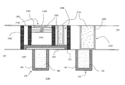
- the last process steps are illustrated in FIG. 31 .
- the photoresist mask 2802 is removed from the F-RAM contact stud structure 3100 using the same O 2 plasma ash etching technique as used earlier.
- Ti/TiN liners 3102 are deposited onto opening 2902 , opening 2904 , and opening 3002 followed by an application of a CVD tungsten 3104 layer over the entire surface of the F-RAM contact stud structure 3100 , followed by a CMP process to polish back and planarize the CVD tungsten 3104 back to the level of the thick oxide 202 .
- contact stud 3106 contacts the Ti/TiN 2602 layer and consequently the TE 2502 layer.
- contact stud 3108 contacts the base of the platinum 1302 which is on the other side of the F-RAM structure and between the Al 2 O 3 spacers 2302 and 702 as illustrated.
- the terms “comprises”, “comprising”, or any other variation thereof, are intended to cover a non-exclusive inclusion, such that a process, method, article, or apparatus that comprises a recitation of certain elements does not necessarily include only those elements but may include other elements not expressly recited or inherent to such process, method, article or apparatus. None of the description in the present application should be read as implying that any particular element, step, or function is an essential element which must be included in the claim scope and THE SCOPE OF THE PATENTED SUBJECT MATTER IS DEFINED ONLY BY THE CLAIMS AS ALLOWED. Moreover, none of the appended claims are intended to invoke paragraph six of 35 U.S.C. Sect. 112 unless the exact phrase “means for” is employed and is followed by a participle.
Abstract
Description
Claims (71)
Priority Applications (4)
| Application Number | Priority Date | Filing Date | Title |
|---|---|---|---|
| US13/569,735 US8552515B2 (en) | 2011-08-12 | 2012-08-08 | Method for fabricating a damascene self-aligned ferroelectric random access memory (F-RAM) device structure employing reduced processing steps |
| CN201210287692.3A CN102956566B (en) | 2011-08-12 | 2012-08-13 | Manufacture the method inlaying formula autoregistration ferroelectric RAM device structure |
| US14/010,174 US9318693B2 (en) | 2011-08-12 | 2013-08-26 | Method for fabricating a damascene self-aligned ferroelectric random access memory (F-RAM) having a ferroelectric capacitor aligned with a three dimensional transistor structure |
| US14/026,118 US10347829B1 (en) | 2011-08-12 | 2013-09-13 | Method for fabricating a damascene self-aligned ferroelectric random access memory (F-RAM) device structure employing reduced processing steps |
Applications Claiming Priority (2)
| Application Number | Priority Date | Filing Date | Title |
|---|---|---|---|
| US201161522953P | 2011-08-12 | 2011-08-12 | |
| US13/569,735 US8552515B2 (en) | 2011-08-12 | 2012-08-08 | Method for fabricating a damascene self-aligned ferroelectric random access memory (F-RAM) device structure employing reduced processing steps |
Related Child Applications (1)
| Application Number | Title | Priority Date | Filing Date |
|---|---|---|---|
| US14/026,118 Continuation US10347829B1 (en) | 2011-08-12 | 2013-09-13 | Method for fabricating a damascene self-aligned ferroelectric random access memory (F-RAM) device structure employing reduced processing steps |
Publications (2)
| Publication Number | Publication Date |
|---|---|
| US20130037897A1 US20130037897A1 (en) | 2013-02-14 |
| US8552515B2 true US8552515B2 (en) | 2013-10-08 |
Family
ID=47677001
Family Applications (2)
| Application Number | Title | Priority Date | Filing Date |
|---|---|---|---|
| US13/569,735 Active US8552515B2 (en) | 2011-08-12 | 2012-08-08 | Method for fabricating a damascene self-aligned ferroelectric random access memory (F-RAM) device structure employing reduced processing steps |
| US14/026,118 Active 2032-09-11 US10347829B1 (en) | 2011-08-12 | 2013-09-13 | Method for fabricating a damascene self-aligned ferroelectric random access memory (F-RAM) device structure employing reduced processing steps |
Family Applications After (1)
| Application Number | Title | Priority Date | Filing Date |
|---|---|---|---|
| US14/026,118 Active 2032-09-11 US10347829B1 (en) | 2011-08-12 | 2013-09-13 | Method for fabricating a damascene self-aligned ferroelectric random access memory (F-RAM) device structure employing reduced processing steps |
Country Status (2)
| Country | Link |
|---|---|
| US (2) | US8552515B2 (en) |
| CN (1) | CN102956566B (en) |
Cited By (3)
| Publication number | Priority date | Publication date | Assignee | Title |
|---|---|---|---|---|
| US9305995B1 (en) | 2015-06-01 | 2016-04-05 | Cypress Semiconductor Corporation | Methods of fabricating an F-RAM |
| US9515075B1 (en) | 2015-08-31 | 2016-12-06 | Cypress Semiconductor Corporation | Method for fabricating ferroelectric random-access memory on pre-patterned bottom electrode and oxidation barrier |
| US9548348B2 (en) | 2013-06-27 | 2017-01-17 | Cypress Semiconductor Corporation | Methods of fabricating an F-RAM |
Families Citing this family (1)
| Publication number | Priority date | Publication date | Assignee | Title |
|---|---|---|---|---|
| KR102098017B1 (en) | 2013-12-26 | 2020-04-13 | 에스케이하이닉스 주식회사 | Resistive memory device and method for fabricating the same |
Citations (18)
| Publication number | Priority date | Publication date | Assignee | Title |
|---|---|---|---|---|
| US4888733A (en) | 1988-09-12 | 1989-12-19 | Ramtron Corporation | Non-volatile memory cell and sensing method |
| US4914627A (en) | 1987-07-02 | 1990-04-03 | Ramtron Corporation | One transistor memory cell with programmable capacitance divider |
| US5394367A (en) | 1994-03-18 | 1995-02-28 | Ramtron International Corporation | System and method for write-protecting predetermined portions of a memory array |
| US5638319A (en) * | 1995-06-05 | 1997-06-10 | Sharp Kabushiki Kaisha | Non-volatile random access memory and fabrication method thereof |
| US5864932A (en) | 1996-08-20 | 1999-02-02 | Ramtron International Corporation | Partially or completely encapsulated top electrode of a ferroelectric capacitor |
| US5920453A (en) | 1996-08-20 | 1999-07-06 | Ramtron International Corporation | Completely encapsulated top electrode of a ferroelectric capacitor |
| US5990513A (en) | 1996-10-08 | 1999-11-23 | Ramtron International Corporation | Yield enhancement technique for integrated circuit processing to reduce effects of undesired dielectric moisture retention and subsequent hydrogen out-diffusion |
| US6027947A (en) | 1996-08-20 | 2000-02-22 | Ramtron International Corporation | Partially or completely encapsulated top electrode of a ferroelectric capacitor |
| US6153460A (en) * | 1998-12-28 | 2000-11-28 | Sharp Kabushiki Kaisha | Method of fabricating semiconductor memory device |
| US6174735B1 (en) | 1998-10-23 | 2001-01-16 | Ramtron International Corporation | Method of manufacturing ferroelectric memory device useful for preventing hydrogen line degradation |
| US6211542B1 (en) | 1996-08-20 | 2001-04-03 | Ramtron International Corporation | Completely encapsulated top electrode of a ferroelectric capacitor using a lead-enhanced escapsulation layer |
| US6242299B1 (en) | 1999-04-01 | 2001-06-05 | Ramtron International Corporation | Barrier layer to protect a ferroelectric capacitor after contact has been made to the capacitor electrode |
| US6249014B1 (en) | 1998-10-01 | 2001-06-19 | Ramtron International Corporation | Hydrogen barrier encapsulation techniques for the control of hydrogen induced degradation of ferroelectric capacitors in conjunction with multilevel metal processing for non-volatile integrated circuit memory devices |
| US6376259B1 (en) | 2001-03-21 | 2002-04-23 | Ramtron International Corporation | Method for manufacturing a ferroelectric memory cell including co-annealing |
| US6423592B1 (en) | 2001-06-26 | 2002-07-23 | Ramtron International Corporation | PZT layer as a temporary encapsulation and hard mask for a ferroelectric capacitor |
| US6492673B1 (en) | 2001-05-22 | 2002-12-10 | Ramtron International Corporation | Charge pump or other charge storage capacitor including PZT layer for combined use as encapsulation layer and dielectric layer of ferroelectric capacitor and a method for manufacturing the same |
| US6495413B2 (en) | 2001-02-28 | 2002-12-17 | Ramtron International Corporation | Structure for masking integrated capacitors of particular utility for ferroelectric memory integrated circuits |
| US6597028B2 (en) | 2000-06-26 | 2003-07-22 | Ramtron International Corporation | Capacitively coupled ferroelectric random access memory cell and a method for manufacturing the same |
Family Cites Families (12)
| Publication number | Priority date | Publication date | Assignee | Title |
|---|---|---|---|---|
| JP3412051B2 (en) | 1993-05-14 | 2003-06-03 | 日本テキサス・インスツルメンツ株式会社 | Capacitor |
| US6509601B1 (en) * | 1998-07-31 | 2003-01-21 | Samsung Electronics Co., Ltd. | Semiconductor memory device having capacitor protection layer and method for manufacturing the same |
| TW508808B (en) | 2001-09-14 | 2002-11-01 | Winbond Electronics Corp | Stacked type capacitor structure and its manufacturing method |
| KR100487558B1 (en) | 2003-03-03 | 2005-05-03 | 삼성전자주식회사 | Ferroelectric memory device equipped with semi-cylindrical capacitor and method for thereof |
| KR100560803B1 (en) | 2004-02-04 | 2006-03-13 | 삼성전자주식회사 | Semiconductor devices having capacitors and methods of fabricating the same |
| EP1624479A3 (en) | 2004-08-05 | 2008-07-16 | Samsung Electronics Co, Ltd | Ferroelectric memory and ferroelectric capacitor with Ir-alloy electrode or Ru-alloy electrode and method of manufacturing same |
| DE102005004376A1 (en) | 2005-01-31 | 2006-08-10 | Infineon Technologies Ag | Semiconductor memory device e.g. high-density chain-ferroelectric RAM, has capacitor arrangement with capacitors serving as memory units, where memory units and capacitors are separated from each other by insulation area |
| KR100707181B1 (en) | 2005-02-14 | 2007-04-13 | 삼성전자주식회사 | Semiconductor memory device with dual storage node and methods of manufacturing and operating the same |
| JP2006352005A (en) | 2005-06-20 | 2006-12-28 | Toshiba Corp | Ferroelectric storage device and method for manufacturing the same |
| KR100718137B1 (en) * | 2005-09-05 | 2007-05-14 | 삼성전자주식회사 | Ferroelectric capacitor having 3D structure, nonvolatile memory device comprising the same and method of manufacturing the same |
| JP2008205300A (en) | 2007-02-21 | 2008-09-04 | Toshiba Corp | Semiconductor device and manufacturing method of semiconductor device |
| US8507353B2 (en) | 2010-08-11 | 2013-08-13 | Samsung Electronics Co., Ltd. | Method of forming semiconductor device having self-aligned plug |
-
2012
- 2012-08-08 US US13/569,735 patent/US8552515B2/en active Active
- 2012-08-13 CN CN201210287692.3A patent/CN102956566B/en active Active
-
2013
- 2013-09-13 US US14/026,118 patent/US10347829B1/en active Active
Patent Citations (24)
| Publication number | Priority date | Publication date | Assignee | Title |
|---|---|---|---|---|
| US4914627A (en) | 1987-07-02 | 1990-04-03 | Ramtron Corporation | One transistor memory cell with programmable capacitance divider |
| US4888733A (en) | 1988-09-12 | 1989-12-19 | Ramtron Corporation | Non-volatile memory cell and sensing method |
| US5394367A (en) | 1994-03-18 | 1995-02-28 | Ramtron International Corporation | System and method for write-protecting predetermined portions of a memory array |
| US5638319A (en) * | 1995-06-05 | 1997-06-10 | Sharp Kabushiki Kaisha | Non-volatile random access memory and fabrication method thereof |
| US6281023B2 (en) | 1996-08-20 | 2001-08-28 | Ramtron International Corporation | Completely encapsulated top electrode of a ferroelectric capacitor using a lead-enhanced encapsulation layer |
| US5864932A (en) | 1996-08-20 | 1999-02-02 | Ramtron International Corporation | Partially or completely encapsulated top electrode of a ferroelectric capacitor |
| US5920453A (en) | 1996-08-20 | 1999-07-06 | Ramtron International Corporation | Completely encapsulated top electrode of a ferroelectric capacitor |
| US6211542B1 (en) | 1996-08-20 | 2001-04-03 | Ramtron International Corporation | Completely encapsulated top electrode of a ferroelectric capacitor using a lead-enhanced escapsulation layer |
| US6027947A (en) | 1996-08-20 | 2000-02-22 | Ramtron International Corporation | Partially or completely encapsulated top electrode of a ferroelectric capacitor |
| US6150184A (en) | 1996-08-20 | 2000-11-21 | Ramtron International Corporation | Method of fabricating partially or completely encapsulated top electrode of a ferroelectric capacitor |
| US5990513A (en) | 1996-10-08 | 1999-11-23 | Ramtron International Corporation | Yield enhancement technique for integrated circuit processing to reduce effects of undesired dielectric moisture retention and subsequent hydrogen out-diffusion |
| US6190926B1 (en) | 1996-10-08 | 2001-02-20 | Ramtron International Corporation | Yield enhancement technique for integrated circuit processing to reduce effects of undesired dielectric moisture retention and subsequent hydrogen out-diffusion |
| US6613586B2 (en) * | 1998-10-01 | 2003-09-02 | Ramtron International Corporation | Hydrogen barrier encapsulation techniques for the control of hydrogen induced degradation of ferroelectric capacitors in conjunction with multilevel metal processing for non-volatile integrated circuit memory devices |
| US6249014B1 (en) | 1998-10-01 | 2001-06-19 | Ramtron International Corporation | Hydrogen barrier encapsulation techniques for the control of hydrogen induced degradation of ferroelectric capacitors in conjunction with multilevel metal processing for non-volatile integrated circuit memory devices |
| US6201726B1 (en) | 1998-10-23 | 2001-03-13 | Ramtron International Corporation | Ferroelectric memory device structure useful for preventing hydrogen line degradation |
| US6174735B1 (en) | 1998-10-23 | 2001-01-16 | Ramtron International Corporation | Method of manufacturing ferroelectric memory device useful for preventing hydrogen line degradation |
| US6358755B1 (en) | 1998-10-23 | 2002-03-19 | Ramtron International Corporation | Ferroelectric memory device structure useful for preventing hydrogen line degradation |
| US6153460A (en) * | 1998-12-28 | 2000-11-28 | Sharp Kabushiki Kaisha | Method of fabricating semiconductor memory device |
| US6242299B1 (en) | 1999-04-01 | 2001-06-05 | Ramtron International Corporation | Barrier layer to protect a ferroelectric capacitor after contact has been made to the capacitor electrode |
| US6597028B2 (en) | 2000-06-26 | 2003-07-22 | Ramtron International Corporation | Capacitively coupled ferroelectric random access memory cell and a method for manufacturing the same |
| US6495413B2 (en) | 2001-02-28 | 2002-12-17 | Ramtron International Corporation | Structure for masking integrated capacitors of particular utility for ferroelectric memory integrated circuits |
| US6376259B1 (en) | 2001-03-21 | 2002-04-23 | Ramtron International Corporation | Method for manufacturing a ferroelectric memory cell including co-annealing |
| US6492673B1 (en) | 2001-05-22 | 2002-12-10 | Ramtron International Corporation | Charge pump or other charge storage capacitor including PZT layer for combined use as encapsulation layer and dielectric layer of ferroelectric capacitor and a method for manufacturing the same |
| US6423592B1 (en) | 2001-06-26 | 2002-07-23 | Ramtron International Corporation | PZT layer as a temporary encapsulation and hard mask for a ferroelectric capacitor |
Cited By (5)
| Publication number | Priority date | Publication date | Assignee | Title |
|---|---|---|---|---|
| US9548348B2 (en) | 2013-06-27 | 2017-01-17 | Cypress Semiconductor Corporation | Methods of fabricating an F-RAM |
| US9305995B1 (en) | 2015-06-01 | 2016-04-05 | Cypress Semiconductor Corporation | Methods of fabricating an F-RAM |
| US9646976B2 (en) | 2015-06-01 | 2017-05-09 | Cypress Semiconductor Corporation | Ferroelectric random-access memory with pre-patterned oxygen barrier |
| US9515075B1 (en) | 2015-08-31 | 2016-12-06 | Cypress Semiconductor Corporation | Method for fabricating ferroelectric random-access memory on pre-patterned bottom electrode and oxidation barrier |
| US10079240B2 (en) | 2015-08-31 | 2018-09-18 | Cypress Semiconductor Corporation | Ferroelectric random-access memory on pre-patterned bottom electrode and oxidation barrier |
Also Published As
| Publication number | Publication date |
|---|---|
| US10347829B1 (en) | 2019-07-09 |
| CN102956566A (en) | 2013-03-06 |
| CN102956566B (en) | 2016-06-15 |
| US20130037897A1 (en) | 2013-02-14 |
Similar Documents
| Publication | Publication Date | Title |
|---|---|---|
| US8518792B2 (en) | Method for fabricating a damascene self-aligned ferroelectric random access memory (F-RAM) having a ferroelectric capacitor aligned with a three dimensional transistor structure | |
| US6337496B2 (en) | Ferroelectric capacitor | |
| US7173301B2 (en) | Ferroelectric memory device with merged-top-plate structure and method for fabricating the same | |
| US11729993B2 (en) | Ferroelectric random access memory (FRAM) capacitors and methods of construction | |
| US10347829B1 (en) | Method for fabricating a damascene self-aligned ferroelectric random access memory (F-RAM) device structure employing reduced processing steps | |
| US8728901B2 (en) | Method for fabricating a damascene self-aligned ferroelectric random access memory (F-RAM) with simultaneous formation of sidewall ferroelectric capacitors | |
| US20080076191A1 (en) | GCIB smoothing of the contact level to improve PZT films | |
| US6583507B1 (en) | Barrier for capacitor over plug structures | |
| US6911362B2 (en) | Methods for forming electronic devices including capacitor structures | |
| US7419837B2 (en) | Method of manufacturing semiconductor device | |
| US6724026B2 (en) | Memory architecture with memory cell groups | |
| US20040232457A1 (en) | Memory architecture with series grouped by cells | |
| US20060214206A1 (en) | Ferroelectric memory device and method of manufacturing the same | |
| US20030139006A1 (en) | Method for producing capacitor structures | |
| US11937434B2 (en) | Ferroelectric random access memory (FRAM) capacitors and methods of construction | |
| US6785119B2 (en) | Ferroelectric capacitor and process for its manufacture | |
| US6734057B2 (en) | Method of patterning capacitors and capacitors made thereby | |
| US11393833B2 (en) | Ferroelectric random access memory device with seed layer | |
| US7122441B2 (en) | Method of fabricating a plurality of ferroelectric capacitors | |
| CN116686431A (en) | Ferroelectric Random Access Memory (FRAM) capacitor and method of construction |
Legal Events
| Date | Code | Title | Description |
|---|---|---|---|
| AS | Assignment |
Owner name: RAMTRON INTERNATIONAL CORPORATION, COLORADO Free format text: ASSIGNMENT OF ASSIGNORS INTEREST;ASSIGNORS:SUN, SHAN;DAVENPORT, THOMAS E.;CRONIN, JOHN;SIGNING DATES FROM 20120804 TO 20120813;REEL/FRAME:028948/0165 |
|
| AS | Assignment |
Owner name: CYPRESS SEMICONDUCTOR CORPORATION, CALIFORNIA Free format text: ASSIGNMENT OF ASSIGNORS INTEREST;ASSIGNOR:RAMTRON INTERNATIONAL CORPORATION;REEL/FRAME:029408/0437 Effective date: 20121203 |
|
| STCF | Information on status: patent grant |
Free format text: PATENTED CASE |
|
| AS | Assignment |
Owner name: MORGAN STANLEY SENIOR FUNDING, INC., NEW YORK Free format text: SECURITY INTEREST;ASSIGNORS:CYPRESS SEMICONDUCTOR CORPORATION;SPANSION LLC;REEL/FRAME:035240/0429 Effective date: 20150312 |
|
| FPAY | Fee payment |
Year of fee payment: 4 |
|
| AS | Assignment |
Owner name: MUFG UNION BANK, N.A., CALIFORNIA Free format text: ASSIGNMENT AND ASSUMPTION OF SECURITY INTEREST IN INTELLECTUAL PROPERTY;ASSIGNOR:MORGAN STANLEY SENIOR FUNDING, INC.;REEL/FRAME:050896/0366 Effective date: 20190731 |
|
| AS | Assignment |
Owner name: MORGAN STANLEY SENIOR FUNDING, INC., NEW YORK Free format text: CORRECTIVE ASSIGNMENT TO CORRECT THE 8647899 PREVIOUSLY RECORDED ON REEL 035240 FRAME 0429. ASSIGNOR(S) HEREBY CONFIRMS THE SECURITY INTERST;ASSIGNORS:CYPRESS SEMICONDUCTOR CORPORATION;SPANSION LLC;REEL/FRAME:058002/0470 Effective date: 20150312 |
|
| MAFP | Maintenance fee payment |
Free format text: PAYMENT OF MAINTENANCE FEE, 8TH YEAR, LARGE ENTITY (ORIGINAL EVENT CODE: M1552); ENTITY STATUS OF PATENT OWNER: LARGE ENTITY Year of fee payment: 8 |
|
| AS | Assignment |
Owner name: SPANSION LLC, CALIFORNIA Free format text: RELEASE BY SECURED PARTY;ASSIGNOR:MUFG UNION BANK, N.A.;REEL/FRAME:059410/0438 Effective date: 20200416 Owner name: CYPRESS SEMICONDUCTOR CORPORATION, CALIFORNIA Free format text: RELEASE BY SECURED PARTY;ASSIGNOR:MUFG UNION BANK, N.A.;REEL/FRAME:059410/0438 Effective date: 20200416 |
|
| AS | Assignment |
Owner name: INFINEON TECHNOLOGIES LLC, CALIFORNIA Free format text: ASSIGNMENT OF ASSIGNORS INTEREST;ASSIGNOR:CYPRESS SEMICONDUCTOR CORPORATION;REEL/FRAME:059721/0467 Effective date: 20200315 |