US8552708B2 - Monolithic DC/DC power management module with surface FET - Google Patents
Monolithic DC/DC power management module with surface FET Download PDFInfo
- Publication number
- US8552708B2 US8552708B2 US13/152,222 US201113152222A US8552708B2 US 8552708 B2 US8552708 B2 US 8552708B2 US 201113152222 A US201113152222 A US 201113152222A US 8552708 B2 US8552708 B2 US 8552708B2
- Authority
- US
- United States
- Prior art keywords
- converter
- inductor
- fet
- magnetic core
- amorphous silica
- Prior art date
- Legal status (The legal status is an assumption and is not a legal conclusion. Google has not performed a legal analysis and makes no representation as to the accuracy of the status listed.)
- Expired - Fee Related, expires
Links
- 239000004065 semiconductor Substances 0.000 claims abstract description 60
- 238000004804 winding Methods 0.000 claims abstract description 53
- 239000000758 substrate Substances 0.000 claims abstract description 37
- 239000011162 core material Substances 0.000 claims description 60
- 239000000463 material Substances 0.000 claims description 42
- VYPSYNLAJGMNEJ-UHFFFAOYSA-N Silicium dioxide Chemical compound O=[Si]=O VYPSYNLAJGMNEJ-UHFFFAOYSA-N 0.000 claims description 27
- 239000003990 capacitor Substances 0.000 claims description 22
- 239000000919 ceramic Substances 0.000 claims description 21
- 230000035699 permeability Effects 0.000 claims description 18
- 239000004020 conductor Substances 0.000 claims description 14
- 229910052710 silicon Inorganic materials 0.000 claims description 6
- 239000010703 silicon Substances 0.000 claims description 6
- 150000001875 compounds Chemical class 0.000 claims description 4
- 239000011248 coating agent Substances 0.000 claims description 2
- 238000000576 coating method Methods 0.000 claims description 2
- 238000000034 method Methods 0.000 description 36
- 230000036961 partial effect Effects 0.000 description 19
- 238000004891 communication Methods 0.000 description 17
- QZZYPHBVOQMBAT-JTQLQIEISA-N (2s)-2-amino-3-[4-(2-fluoroethoxy)phenyl]propanoic acid Chemical compound OC(=O)[C@@H](N)CC1=CC=C(OCCF)C=C1 QZZYPHBVOQMBAT-JTQLQIEISA-N 0.000 description 13
- 238000000151 deposition Methods 0.000 description 13
- 238000004519 manufacturing process Methods 0.000 description 13
- 238000013461 design Methods 0.000 description 11
- 239000003989 dielectric material Substances 0.000 description 11
- 230000004907 flux Effects 0.000 description 10
- 239000002184 metal Substances 0.000 description 8
- 235000012431 wafers Nutrition 0.000 description 8
- 229910052751 metal Inorganic materials 0.000 description 7
- 239000000126 substance Substances 0.000 description 7
- 239000000203 mixture Substances 0.000 description 6
- 230000007246 mechanism Effects 0.000 description 5
- 239000002243 precursor Substances 0.000 description 5
- 230000008569 process Effects 0.000 description 5
- XUIMIQQOPSSXEZ-UHFFFAOYSA-N Silicon Chemical compound [Si] XUIMIQQOPSSXEZ-UHFFFAOYSA-N 0.000 description 4
- 230000008901 benefit Effects 0.000 description 4
- 230000015556 catabolic process Effects 0.000 description 4
- 230000001143 conditioned effect Effects 0.000 description 4
- 238000010276 construction Methods 0.000 description 4
- 238000010586 diagram Methods 0.000 description 3
- 238000006073 displacement reaction Methods 0.000 description 3
- 230000006872 improvement Effects 0.000 description 3
- 230000010354 integration Effects 0.000 description 3
- 239000007788 liquid Substances 0.000 description 3
- 239000012705 liquid precursor Substances 0.000 description 3
- 238000004151 rapid thermal annealing Methods 0.000 description 3
- 239000007787 solid Substances 0.000 description 3
- 238000005507 spraying Methods 0.000 description 3
- 229910000601 superalloy Inorganic materials 0.000 description 3
- 229910000859 α-Fe Inorganic materials 0.000 description 3
- 239000004215 Carbon black (E152) Substances 0.000 description 2
- 229910045601 alloy Inorganic materials 0.000 description 2
- 239000000956 alloy Substances 0.000 description 2
- 238000000137 annealing Methods 0.000 description 2
- 230000000712 assembly Effects 0.000 description 2
- 238000000429 assembly Methods 0.000 description 2
- 229910010293 ceramic material Inorganic materials 0.000 description 2
- 238000005234 chemical deposition Methods 0.000 description 2
- 239000002131 composite material Substances 0.000 description 2
- 239000010949 copper Substances 0.000 description 2
- 230000007547 defect Effects 0.000 description 2
- 230000008021 deposition Effects 0.000 description 2
- 238000011161 development Methods 0.000 description 2
- 230000005669 field effect Effects 0.000 description 2
- 229930195733 hydrocarbon Natural products 0.000 description 2
- 150000002430 hydrocarbons Chemical class 0.000 description 2
- 239000012212 insulator Substances 0.000 description 2
- 239000000395 magnesium oxide Substances 0.000 description 2
- CPLXHLVBOLITMK-UHFFFAOYSA-N magnesium oxide Inorganic materials [Mg]=O CPLXHLVBOLITMK-UHFFFAOYSA-N 0.000 description 2
- AXZKOIWUVFPNLO-UHFFFAOYSA-N magnesium;oxygen(2-) Chemical compound [O-2].[Mg+2] AXZKOIWUVFPNLO-UHFFFAOYSA-N 0.000 description 2
- 239000000696 magnetic material Substances 0.000 description 2
- 230000000737 periodic effect Effects 0.000 description 2
- 239000000843 powder Substances 0.000 description 2
- 238000012545 processing Methods 0.000 description 2
- 229910052721 tungsten Inorganic materials 0.000 description 2
- JBRZTFJDHDCESZ-UHFFFAOYSA-N AsGa Chemical compound [As]#[Ga] JBRZTFJDHDCESZ-UHFFFAOYSA-N 0.000 description 1
- RYGMFSIKBFXOCR-UHFFFAOYSA-N Copper Chemical compound [Cu] RYGMFSIKBFXOCR-UHFFFAOYSA-N 0.000 description 1
- QPLDLSVMHZLSFG-UHFFFAOYSA-N Copper oxide Chemical compound [Cu]=O QPLDLSVMHZLSFG-UHFFFAOYSA-N 0.000 description 1
- 239000005751 Copper oxide Substances 0.000 description 1
- 229910005540 GaP Inorganic materials 0.000 description 1
- JMASRVWKEDWRBT-UHFFFAOYSA-N Gallium nitride Chemical compound [Ga]#N JMASRVWKEDWRBT-UHFFFAOYSA-N 0.000 description 1
- 229910001374 Invar Inorganic materials 0.000 description 1
- ZOKXTWBITQBERF-UHFFFAOYSA-N Molybdenum Chemical compound [Mo] ZOKXTWBITQBERF-UHFFFAOYSA-N 0.000 description 1
- XLOMVQKBTHCTTD-UHFFFAOYSA-N Zinc monoxide Chemical compound [Zn]=O XLOMVQKBTHCTTD-UHFFFAOYSA-N 0.000 description 1
- 239000002253 acid Substances 0.000 description 1
- 239000000853 adhesive Substances 0.000 description 1
- 230000001070 adhesive effect Effects 0.000 description 1
- 230000002411 adverse Effects 0.000 description 1
- 230000009286 beneficial effect Effects 0.000 description 1
- 230000015572 biosynthetic process Effects 0.000 description 1
- 230000000295 complement effect Effects 0.000 description 1
- 239000012141 concentrate Substances 0.000 description 1
- 230000003750 conditioning effect Effects 0.000 description 1
- 229910052802 copper Inorganic materials 0.000 description 1
- 229910000431 copper oxide Inorganic materials 0.000 description 1
- 230000008878 coupling Effects 0.000 description 1
- 238000010168 coupling process Methods 0.000 description 1
- 238000005859 coupling reaction Methods 0.000 description 1
- 238000000354 decomposition reaction Methods 0.000 description 1
- 238000009826 distribution Methods 0.000 description 1
- 238000005516 engineering process Methods 0.000 description 1
- 239000011521 glass Substances 0.000 description 1
- 230000020169 heat generation Effects 0.000 description 1
- 239000012943 hotmelt Substances 0.000 description 1
- 239000012535 impurity Substances 0.000 description 1
- 230000009191 jumping Effects 0.000 description 1
- 229910000833 kovar Inorganic materials 0.000 description 1
- 230000005381 magnetic domain Effects 0.000 description 1
- 238000012423 maintenance Methods 0.000 description 1
- 229910001092 metal group alloy Inorganic materials 0.000 description 1
- 229910044991 metal oxide Inorganic materials 0.000 description 1
- 150000004706 metal oxides Chemical class 0.000 description 1
- 150000002739 metals Chemical class 0.000 description 1
- 238000012986 modification Methods 0.000 description 1
- 230000004048 modification Effects 0.000 description 1
- 229910052750 molybdenum Inorganic materials 0.000 description 1
- 239000011733 molybdenum Substances 0.000 description 1
- 238000012544 monitoring process Methods 0.000 description 1
- 230000036963 noncompetitive effect Effects 0.000 description 1
- -1 organic acid salts Chemical class 0.000 description 1
- 150000002902 organometallic compounds Chemical class 0.000 description 1
- 238000000059 patterning Methods 0.000 description 1
- 229910000889 permalloy Inorganic materials 0.000 description 1
- 230000000135 prohibitive effect Effects 0.000 description 1
- 238000007670 refining Methods 0.000 description 1
- 230000001105 regulatory effect Effects 0.000 description 1
- 150000003839 salts Chemical class 0.000 description 1
- 239000002904 solvent Substances 0.000 description 1
- 238000009718 spray deposition Methods 0.000 description 1
- 238000012546 transfer Methods 0.000 description 1
- WFKWXMTUELFFGS-UHFFFAOYSA-N tungsten Chemical compound [W] WFKWXMTUELFFGS-UHFFFAOYSA-N 0.000 description 1
- 239000010937 tungsten Substances 0.000 description 1
Images


Classifications
-
- H—ELECTRICITY
- H01—ELECTRIC ELEMENTS
- H01F—MAGNETS; INDUCTANCES; TRANSFORMERS; SELECTION OF MATERIALS FOR THEIR MAGNETIC PROPERTIES
- H01F17/00—Fixed inductances of the signal type
- H01F17/04—Fixed inductances of the signal type with magnetic core
- H01F17/06—Fixed inductances of the signal type with magnetic core with core substantially closed in itself, e.g. toroid
- H01F17/062—Toroidal core with turns of coil around it
-
- H—ELECTRICITY
- H01—ELECTRIC ELEMENTS
- H01F—MAGNETS; INDUCTANCES; TRANSFORMERS; SELECTION OF MATERIALS FOR THEIR MAGNETIC PROPERTIES
- H01F27/00—Details of transformers or inductances, in general
- H01F27/28—Coils; Windings; Conductive connections
- H01F27/2804—Printed windings
-
- H—ELECTRICITY
- H01—ELECTRIC ELEMENTS
- H01L—SEMICONDUCTOR DEVICES NOT COVERED BY CLASS H10
- H01L23/00—Details of semiconductor or other solid state devices
- H01L23/58—Structural electrical arrangements for semiconductor devices not otherwise provided for, e.g. in combination with batteries
- H01L23/64—Impedance arrangements
- H01L23/645—Inductive arrangements
-
- H—ELECTRICITY
- H01—ELECTRIC ELEMENTS
- H01L—SEMICONDUCTOR DEVICES NOT COVERED BY CLASS H10
- H01L25/00—Assemblies consisting of a plurality of individual semiconductor or other solid state devices ; Multistep manufacturing processes thereof
- H01L25/16—Assemblies consisting of a plurality of individual semiconductor or other solid state devices ; Multistep manufacturing processes thereof the devices being of types provided for in two or more different main groups of groups H01L27/00 - H01L33/00, or in a single subclass of H10K, H10N, e.g. forming hybrid circuits
-
- H—ELECTRICITY
- H01—ELECTRIC ELEMENTS
- H01F—MAGNETS; INDUCTANCES; TRANSFORMERS; SELECTION OF MATERIALS FOR THEIR MAGNETIC PROPERTIES
- H01F27/00—Details of transformers or inductances, in general
- H01F27/28—Coils; Windings; Conductive connections
- H01F27/2804—Printed windings
- H01F2027/2814—Printed windings with only part of the coil or of the winding in the printed circuit board, e.g. the remaining coil or winding sections can be made of wires or sheets
-
- H—ELECTRICITY
- H01—ELECTRIC ELEMENTS
- H01L—SEMICONDUCTOR DEVICES NOT COVERED BY CLASS H10
- H01L2924/00—Indexing scheme for arrangements or methods for connecting or disconnecting semiconductor or solid-state bodies as covered by H01L24/00
- H01L2924/0001—Technical content checked by a classifier
- H01L2924/0002—Not covered by any one of groups H01L24/00, H01L24/00 and H01L2224/00
-
- H—ELECTRICITY
- H02—GENERATION; CONVERSION OR DISTRIBUTION OF ELECTRIC POWER
- H02M—APPARATUS FOR CONVERSION BETWEEN AC AND AC, BETWEEN AC AND DC, OR BETWEEN DC AND DC, AND FOR USE WITH MAINS OR SIMILAR POWER SUPPLY SYSTEMS; CONVERSION OF DC OR AC INPUT POWER INTO SURGE OUTPUT POWER; CONTROL OR REGULATION THEREOF
- H02M7/00—Conversion of ac power input into dc power output; Conversion of dc power input into ac power output
- H02M7/003—Constructional details, e.g. physical layout, assembly, wiring or busbar connections
Definitions
- the present invention generally relates to DC/DC power management devices configured as a fully integrated system on a semiconductor chip, and in particular to such devices that modulate the drawn power with a planar MOSFET switch and diode embedded in the semiconductor upon which the device is integrated.
- DC/DC power management systems generally regulate DC power supplied from a battery at a particular voltage/current by conditioning the output voltage and current to levels that are appropriate for a particular circuit. It is also desirable to extend the battery life of mobile platforms by using the power management device to selectively turning off a given circuit during time intervals when its functions are not absolutely needed by the larger system it serves. Since most mobile electronic systems will comprise a plurality of circuits that each operate at a variety of voltage and current levels different from those supplied by the battery, a plurality of DC/DC power management systems are required to assure each distinct circuit is operating with well conditioned power. The overall system's power efficiency is optimized and costs are minimized by using low loss DC/DC power management modules that are fully integrated at the semiconductor wafer scale.
- DC/DC power management systems may be configured in various control topologies: buck, boost, buck-boost, Luo (positive and negative type), Ca, transformer-type (forward, fly-back, zeta), and super-lift (positive, negative, positive push-pull, negative push-pull, double/enhanced circuit), among others.
- Common features to all these systems include: one or more passive components (resistor or capacitor), at least one power switch, at least one diode, and either at least one inductor coil, transformer coil, or both. (See FIG. 1 ).
- the discrete assembly of these individual components is an obstacle to increasing power density, reducing form factor (size), lowering cost, improving reliability, and improving power efficiency. It is therefore the principal aim of the present invention to improve these system parameters by eliminating any and all discretely assembled components from the fabrication process. It is herein understood that this invention applies to all DC/DC power management systems, irrespective of the control topology or circuit application.
- EMI Electrical loss and electromagnetic interference
- Inductor/transformer coils are usually the largest component of the DC/DC converter systems and the principal cause of electrical loss and EMI. Technologies that have the potential to drive power management circuits at higher switching speeds will reduce the inductor/transformer coil's required inductance and, therefore, lower the coil's size. Large EMI is undesirable because it can destabilize circuit settling times.
- EMI is largely a property of specific coil designs that do not form a closed path for their magnetic current. EMI is also generated by magnetic flux creep and proximity losses, which are also intrinsic qualities of the coil's design.
- a higher loss adds an additional system constraint, as the lost power is converted into heat, which must be managed to maintain stable performance of the modulating power switch.
- Magnetic component core loss is the primary obstacle to achieving acceptable transformer efficiencies ( ⁇ 90%) in high speed, high power switched mode power supplies (“SMPS”), because they increase as the square of the operating frequency. A 10-fold increase in the switching frequency results in 100-fold increase in eddy current power loss.
- SMPS high power switched mode power supplies
- Eddy current loss in the magnetic core also imposes a practical limit on switching speed and circuit form factor.
- transformer coils are often designed to handle smaller magnetic flux swings (lower power) at higher frequencies to avoid excessive loss.
- magnetic core losses in commercial ferrite ceramics currently limit power management module switching frequencies to values between 5-10 MHz.
- Eddy ⁇ ⁇ current ⁇ ⁇ loss V p 2 R E ⁇ t p T ( 2 )
- R E is the ac resistance experienced by eddy currents circulating in the magnetic core
- t p is the width of the pulse that keeps the switch in its “on” or “closed” mode
- T is the time period of the switch duty cycle. Since higher switching speeds enable the use of circuit components with smaller inductance values and further power management module miniaturization, it is therefore desirable to minimize magnetic core loss to the greatest extent possible.
- Hopper et al. U.S. Pat. No. 7,652,348 B1, “APPARATUS & METHOD FOR WAFER LEVEL FABRICATION OF HIGH VALUE INDUCTORS ON SEMICONDUCTOR IC's”, issued Jan. 1, 26, 2010, (Hopper et al. '348) teach the assembly of inductor coils on semiconductor wafers containing active devices buried beneath the wafer surface using high permeability magnetic core material prepared from powder pastes, but does not instruct methods enable a low-loss magnetic core that operates at switching frequencies above 10 MHz.
- active component is herein understood to refer to its conventional definition as an element of an electrical circuit that that does require electrical power to operate and is capable of producing power gain.
- amorphous material is herein understood to mean a material that does not comprise a periodic lattice of atomic elements, or lacks mid-range (over distances of 10's of nanometers) to long-range crystalline order (over distances of 100's of nanometers).
- compositional complexity is herein understood to refer to a material, such as a metal or superalloy, compound semiconductor, or ceramic that consists of three (3) or more elements from the periodic table.
- discrete assembly or “discretely assembled” is herein understood to mean the serial construction of an embodiment through the assembly of a plurality of pre-fabricated components that individually comprise a discrete element of the final assembly.
- integrated circuit is herein understood to mean a semiconductor chip into which at least one transistor element has been embedded.
- LCD is herein understood to mean a method that uses liquid precursor solutions to fabricate materials of arbitrary compositional or chemical complexity as an amorphous laminate or free-standing body or as a crystalline laminate or free-standing body that has atomic-scale chemical uniformity and a microstructure that is controllable down to nanoscale dimensions.
- liquid precursor solution is herein understood to mean a solution of hydrocarbon molecules that also contains soluble metalorganic compounds that may or may not be organic acid salts of the hydrocarbon molecules into which they are dissolved.
- microstructure is herein understood to define the elemental composition and physical size of crystalline grains forming a material substance.
- MISFET is herein understood to mean its conventional definition by referencing a metal-insulator-semiconductor field effect transistor.
- mismatched materials is herein understood to define two materials that have dissimilar crystalline lattice structure, or lattice constants that differ by 5% or more, and/or thermal coefficients of expansion that differ by 10% or more.
- MOSFET is herein understood to mean its conventional definition by referencing a metal-oxide-silicon field effect transistor.
- nanoscale is herein understood to define physical dimensions measured in lengths ranging from 1 nanometer (nm) to 100's of nanometers (nm).
- passive component is herein understood to refer to its conventional definition as an element of an electrical circuit that that does not require electrical power to operate and is not capable of producing power gain.
- standard operating temperatures is herein understood to mean the range of temperatures between ⁇ 40° C. and +125° C.
- optical tolerance or “critical tolerance” are herein understood to mean a performance value, such as a capacitance, inductance, or resistance, that varies less than ⁇ 1% over standard operating temperatures.
- the present invention provides a monolithic DC to DC converter, comprising: a semiconductor substrate; a surface FET formed on the semiconductor substrate that modulates currents across a surface of the semiconductor substrate; and a toroidal inductor with a magnetic core formed on the substrate around the FET and having a first winding connected to the FET.
- the first winding may be a primary inductor coil and the converter may comprise a secondary inductor coil formed on the substrate and having windings interleaved between windings of the primary inductor coil.
- the FET may include a circular or arcuate source electrode and an arcuate gate electrode formed peripherally around the source electrode.
- the converter may further comprise a via connecting the source electrode through the substrate to a ground plane.
- the FET may include an arcuate drain electrode formed peripherally to the source and gate electrodes.
- the FET may include a plurality of arcuate drain electrodes formed peripherally at different angular positions around the source and gate electrodes.
- the FET may include passive components formed on the semiconductor substrate within the toroidal inductor and connected to the source, gate or drain electrodes.
- the converter may further comprise an arcuate plate capacitor formed peripherally to the toroidal inductor.
- the converter may further comprise an arcuate diode formed peripherally to the toroidal inductor.
- the magnetic core may be ceramic and formed on the substrate with at least one layer of amorphous silica located between opposing sections of high permeability crystalline core material.
- the toroidal inductor may include a secondary winding having a turn aligned with the at least one layer of amorphous silica.
- the toroidal inductor may include windings that are mechanically constrained.
- the mechanic constraint of the windings may be achieved by a coating of amorphous silica.
- the monolithic DC to DC converter may have a semiconductor substrate containing silicon.
- the monolithic DC to DC converter may have III-V compound semiconductor substrate.
- a magnetic core comprising a ceramic core element formed with at least one layer of amorphous silica located between opposing sections of high permeability crystalline core material, wherein the ceramic element (or core material) has a resistivity >10 4 ohm-cm and a permeability ⁇ 70.
- the ceramic element (or core material) may have a resistivity >10 12 ohm-cm and a permeability ⁇ 200.
- the ceramic core element may be formed with a plurality of amorphous silica layers, each located between opposing sections of crystalline core material.
- the magnetic core may further comprise an electrical conductor winding aligned with the at least one layer of amorphous silica.
- an inductor comprising: a magnetic core formed with a dielectric gap of high-resistivity material located between opposing sections of crystalline core material and an electrical conductor aligned with the dielectric gap.
- the dielectric gap may be amorphous silica.
- the electrical conductor may be a secondary winding of a transformer.
- FIG. 1 is a representative circuit schematic for a DC-DC converter in fly-back configuration
- FIG. 2 is a low loss magnetic ceramic core in accordance with one embodiment of the present invention.
- FIG. 3 is a power management device assembled from discrete component as described in the prior art
- FIGS. 4 A, 4 B, 4 C are side sectional drawings that illustrate how the LCD process is used to form monolithic structures on a substrate.
- FIG. 5 is a sectional view of a mechanically reinforced inductor winding.
- FIG. 6A is a sectional view of an inductor constructed in accordance with another embodiment of the present invention.
- FIGS. 6B and 6C are perspective views of LCD masks used to form the inductor of FIG. 6A .
- FIG. 7 shows a perspective view of a monolithic power management device formed on a semiconductor substrate in accordance with one embodiment of the present invention.
- FIG. 8A shows a top view of the device of FIG. 7 .
- FIG. 8B shows a bottom view of the device of FIG. 7 .
- FIG. 8 C, 8 D, 8 F show limited perspective views of a portion of the device of FIG. 7 .
- FIG. 8E is a circuit diagram of a portion of the device of FIG. 7 .
- FIG. 1 provides a circuit schematic of a DC/DC power management circuit using fly-back configuration.
- a power management system 1 is generally, but not necessarily, comprised of a DC power source 3 that feeds at least one power switch 5 , which modulates the primary current 6 drawn from electrical ground to at least one transformer 7 comprised of a primary inductor coil 9 and a secondary inductor coil 11 .
- Certain topologies may use an inductor coil 9 , 11 in series or parallel connection as opposed to a transformer 7 .
- the output of the primary coil current 6 induces a back emf in the secondary coil that draws secondary current 13 .
- the secondary coil 11 output current flows through a diode 15 , which supplies the circuit's conditioned DC output power 16 and charges a capacitor 17 that supplies current to the secondary coil 11 .
- a switch controller 19 monitors the differential output voltage 16 , power source voltage 3 , and uses those inputs to modulate the power switch 5 .
- different power control circuit topologies will comprise at least one switch 5 , one diode 15 , one capacitor 17 , and one inductor coil 9 , 11 or transformer coil 7 , and one controller circuit 19 . They may additionally comprise other passive (resistor, capacitor, and inductor) or active (diode or transistor switch) components not shown in FIG. 1 that fall under the scope of the present invention.
- a particular aspect of the present invention is to reduce eddy current and other losses in the magnetic core of an inductor or transformer component to drive DC/DC power management circuits at switching frequencies higher than 20 MHz, preferably frequencies higher than 500 MHz, while simultaneously managing large operating voltages, V p .
- Loss tangent, tan ⁇ m in the ferrite ceramic magnetic core materials is generated by the three principal loss mechanisms: hysteresis, eddy current, and residual loss.
- Hysteresis is the dominant loss mechanism at frequencies lower than 100 KHz and can be controlled by selecting suitable compositions and eliminating defects and impurities. Eddy current losses are managed by increasing the resistivity of the magnetic core material. Residual loss is the dominant mechanism at frequencies above 10 MHz and is pronounced when the ceramic grain size is large enough to allow two (2) or more magnetic domains to interact with one another within a single grain.
- LCD liquid chemical deposition
- This ability to formulate high purity metal oxides in high complexity ceramic compositions having atomic scale chemical uniformity eliminates the defects that contribute to hysteresis loss and would be present in powder-processed magnetic cores, whether they are integrated in the semiconductor surface or not.
- the ability to integrate high chemical complexity materials having atomic scale uniformity on the surface of a semiconductor enables the development of high permeability ( ⁇ R ⁇ 70, preferably ⁇ R ⁇ 200) magnetic cores that simultaneously have high resistivity that make the circuit suitable for high frequency operation. Combined, these enable the development of power management circuits that have power densities exceeding 200 W-in ⁇ 3 , and preferably 500 W-in ⁇ 3 .
- the first method utilizes LCD to add non-magnetic elements comprising magnesium oxide (MgO), zinc oxide (ZnO), and copper oxide (Cu) into the ferrite core material to increase its resistivity to levels greater than 10 3 ⁇ -cm, preferably to levels greater than 10 7 ⁇ -cm, while simultaneously holding the desired high permeability, ⁇ R .
- the second method shown in FIG. 2 optionally inserts at least one thin layer of amorphous silica 100 , 100 ′ between layers of high resistivity, high permeability ceramic material 101 A, 101 B, 101 C within the magnetic core 102 formed on the surface of a semiconductor device.
- a principal objective of the amorphous silica layer(s) 100 in combination with the high-resistivity, high permeability ceramic material 101 is to produce a magnetic core having an internal resistance greater than 10 5 ⁇ -cm ⁇ 3 per Watt of acceptable loss at a given switching frequency.
- This level of internal resistance ( ⁇ internal ) will reduce eddy current losses within the magnetic core to levels less than 0.5 mW-cm ⁇ 3 , preferably to loss levels less than or equal to 20 ⁇ W-cm ⁇ 3 .
- These high internal resistance levels enable this aspect of the invention to be applied to managing power levels of 500 W or more.
- Yet another aspect of this invention applies the LCD process to formulate high permeability magnetic material having low residual loss, which is a dominant loss mechanism above 10 MHz.
- This aspect of the invention utilizes LCD's ability to formulate a complex ceramic composition with uniform grain size diameter 103 , wherein 100% of the grains have diameters less than 1.5 ⁇ the mean grain size diameter, and said grain mean size diameter less than 5 ⁇ m, preferably less than 2 ⁇ m.
- a further aspect of this invention relates to the integration of at least one inductor or transformer coil enveloped around a low-loss ( ⁇ 0.5 mW-cm ⁇ 3 ), high permeability ( ⁇ R ⁇ 70) magnetic core material that is fully integrated on to a semiconductor die.
- Fully integrated systems achieve dramatically higher field reliability and sharply lower cost. While transistor assemblies have been integrated into semiconductor die, the inability for powder-based or paste-based ceramic manufacturing to maintain performance values within “critical tolerances” has made system-on-chip passive assemblies, such as those taught by Hopper et al. '348) cost prohibitive due to the inability to rework an out-of-tolerance passive component once it is integrated into a solid state structure.
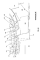
- FIG. 3 depicts a portion of a discretely assembled power management device 110 as taught in the prior art that enables an inductor coil design that is particularly useful in making low EMI transformer coils.
- Conductor traces are screen printed onto both sides of a prefabricated passive dielectric substrate 111 .
- Secondary coil conductor winding traces 112 are printed on the bottom of the dielectric substrate 111
- primary coil conductor winding traces 113 are printed on the top surface of the dielectric substrate 111 .
- a pre-fabricated toroidal magnetic core 114 is mounted to the surface of the dielectric substrate 111 , either by using an adhesive (not shown) or by mechanically fixing it in place with wire bonds that wrap around the toroidal magnetic core 114 to complete the coil windings.
- One set of wire bonds 115 are used to electrically connect the primary coil (P) having turns configured in series.
- a conductive ring 116 to which the secondary coil winding traces 112 are electrically connected, is formed on the bottom of the dielectric substrate 111 .
- the conductive ring 116 allows a second set of wire bonds 117 that wrap around the toroidal magnetic core 114 to form a secondary coil (S) having turns configured in parallel by electrically terminating the secondary winding traces 112 through the second set of wire bonds 117 on a second conductive ring 118 formed on the top surface of the dielectric substrate 111 .
- the upper 118 and lower 116 conductive rings form the terminals for the secondary inductor coil.
- a principal benefit outlined here is that the toroidal magnetic core forms a closed magnetic path that reduces EMI to neighboring components to the power management circuit. Additional benefits include the ability to use a primary coil wound in series and a secondary coil having one or more segments wound in parallel to produce arbitrary turns ratios, including half-turn ratio, if desired. A final benefit is the ability to reduce proximity flux leakage and losses by maintaining equal spacing between windings of the primary and secondary coils, while the use of parallel windings in the secondary coils achieves a number of turns that is electrical different than the primary coil.
- one LCD technique selectively deposits compositionally complex amorphous materials having precise composition and atomic-scale elemental uniformity on a metal, glass or semiconductor substrate 120 by spraying an aerosolized metalorganic precursor solution 121 through a mechanical mask 122 to form a chemically precise amorphous deposit 123 .
- atomic-scale chemical uniformity is achieved by the simultaneous decomposition of the various metalorganic precursor species on the heated substrate surface.
- a deposit having uniform crystalline microstructure 124 wherein 100% of the grains have grain size less than 1.5 ⁇ the mean grain size diameter, is formed by applying a subsequent rapid thermal annealing treatment 125 , preferably a plasma annealing treatment, to the selectively located amorphous deposit 123 .
- This technique is re-applied to selectively deposit additional “mismatched materials” 126 over pre-deposited materials 124 to form integrated monolithic structures by spraying an additional aerosolized metalorganic precursor solution 121 ′ through a different mechanical mask 122 ′.
- Any material deposit may be formed as an amorphous or uniformly crystalline deposit, including a deposit with nanoscale microstructure, as desired for the specific functional purpose of that material deposit.
- LCD permits the construction of monolithic structures on semiconductor substrates having active components buried beneath its surface.
- LCD deposits compositionally complex electroceramics when the deposited materials are processed in oxygenated atmospheres.
- Metals, alloys, superalloys, and semiconductors are integrated into the monolithic structure by processing the applied deposit in oxygen-free atmospheres.
- An alternative LCD technique selectively deposits the material using hot-melt “ink jet” techniques that form a metalorganic wax precursor solid (with all liquid solvent is extracted) on the substrate, that is simultaneously decomposed using a rapid thermal annealing technique, preferably a plasma annealing technique.
- FIGS. 5 thru 6 illustrate specific embodiments that are improvements over the prior art necessary to permit the design and fabrication of fully integrated high power density power management circuits.
- LCD methods are applied to form transformer windings 130 that are mechanically re-enforced as depicted in cross-section in FIG. 5 .
- the mechanically re-enforced transformer windings 130 comprise thin layers of high electrical conductivity material 131 , preferably but not necessarily copper conductor and might also comprise superconducting material, that envelop a hard mechanical constraining member 132 .
- the mechanical constraining member 132 may consist of a hard, low-expansion elemental metal, such as tungsten or molybdenum, or it may comprise an alloy or superalloy, such as kovar, invar, or any other well-known low-expansion expansion material that has a measured hardness value that is at a minimum twice (2 ⁇ ) the measured hardness value of the high electrical conductivity material 131 .
- the thickness 133 of the high conductivity layer 131 should range from 0.5 ⁇ to 10 ⁇ the ac skin depth at the device's optimal operating or switching frequency.
- the coefficient of thermal expansion (CTE) is a critical parameter in the selection of the hard mechanical constraining member 132 , and should match to within 25%, preferably within 10% of the coefficient of thermal expansion of the dielectric material(s) with which the high electrical conductivity material 131 is in physical contact.
- CTE coefficient of thermal expansion
- An additional aspect of the present invention uses amorphous silica as the insulating dielectric 135 to prevent corona discharges (or dielectric breakdown if less strong insulators are used) between windings of the primary and secondary coils.
- a further additional aspect of the present invention utilizes LCD methods to form to form a toroidal magnetic core with gaps in the magnetic material that are filled with an ultra-low loss material, preferably filled with amorphous silica. It is well-known to practitioners skilled in the art of transformer coil design that “air gaps” will concentrate magnetic energy. It is preferred to locate the “air gaps” 140 in regions of the magnetic core 141 that are adjacent to at least one secondary coil winding 142 to increase its power coupling efficiency with energy supplied by the primary coil windings 143 , 143 ′ as shown in FIG. 6A .
- amorphous silica gap material 149 is then applied by spraying silicon metalorganic precursor solution through a complementary mask 150 that only has perforations 151 in the areas where the amorphous silica gap 149 is desired as shown in FIG. 6C .
- the concentration of electromagnetic energy in the transformer is sufficiently powerful to mechanically deform and/or displace the inductor windings if they are not mechanically reinforced. Any such mechanical deformation or displacement will trigger flux jumping and proximity losses and could possibly cause catastrophic failure of the device. It is therefore a specific embodiment of the invention to produce a monolithic structure that has transformer coil windings that are mechanically reinforced by a hard mechanical constraining member 132 that is positioned within the windings' interior and/or by the formation of a mechanically hard insulating dielectric 135 such as amorphous silica.
- the mechanically reinforced transformer coil windings shown in FIGS.
- FIG. 7 depicts another embodiment of the present invention.
- LCD techniques are applied to monolithically integrate a mechanically reinforced toroidal transformer coil having arbitrary turns ratios and minimal proximity and flux leakage loss on the surface of a semiconductor so it maintains electrical communication with at least one embedded high gain surface MOSFET or MISFET power switch, herein after referred to as a surface FET, at least one embedded semiconductor diode, and other passive component structures (as needed) that have been selectively deposited on the semiconductor surface.
- the semiconductor may comprise silicon, it may also preferably consist of any III-V compound semiconductor, such as gallium arsenide (GaAs), gallium nitride (GaN), or indium-gallium phosphide (InGaP).
- GaAs gallium arsenide
- GaN gallium nitride
- InGaP indium-gallium phosphide
- FIG. 7 overviews a monolithic DC-DC power management circuit 200 modulated by a surface FET 204 integrated onto a semiconductor die 202 that functions as the fly-back power management system 1 ( FIG. 1 ).
- a surface FET 204 is embedded in the semiconductor die 202 functions as the power switch 5 ( FIG. 1 ).
- the surface FET 204 is positioned within the empty interior space of toroidal transformer 206 that is formed on the semiconductor die 202 using the LCD methods described above.
- the surface FET 204 modulates current from the DC power source 3 ( FIG. 1 ) to the primary coil 9 ( FIG. 1 ) of the toroidal transformer 206 .
- Current from the DC power source 3 ( FIG. 1 ) is supplied to the monolithic circuit through a backside ground contact 208 .
- An input pad 210 on the top surface of the semiconductor die 202 is used to complete the electrical connection between the transformer's primary coil 9 ( FIG. 1 ) within the toroidal transformer 206 and the DC power source 3 ( FIG. 1 ).
- An output pad 212 on the top surface of the semiconductor die 202 supplies conditioned DC output power 16 that has been regulated by the monolithic DC-DC power management circuit modulated by a surface FET 204 .
- the output pad 212 makes parallel electrical communication to the output of the transformer's secondary coil 11 ( FIG. 1 ) through a diode 15 ( FIG. 1 ), and with a capacitor 17 ( FIG. 1 ) that is jointly connected to ground and the input the input of the transformer's secondary coil 11 ( FIG. 1 ).
- an embedded diode 214 is circumferentially configured over part of the semiconductor surface area exterior to the toroidal transformer 206 .
- One contact (discussed below in greater detail) of the embedded diode 214 is in electrical communication with the output from secondary coil 11 ( FIG.
- the control circuitry 19 may be configured as a surface-mounted controller chip 220 as shown in FIG. 7 ( FIG. 1 ), or it may alternatively be embedded in the semiconductor die (not shown) if its semiconductor material is compatible with those functions and it is economically advantageous to do so.
- a fundamental limitation to discretely assembled power management systems is that the manufacturers of the individual components are economically incentivized in ways that constrain the fully assembled system. For instance, manufacturers of discrete power FETs are economically incentivized to make their devices smaller. The smaller devices are prone to thermal runaway as a given current will induce higher current densities when crammed into the smaller discrete FET volume. This requires the system manufacturer to compensate with improved thermal management systems to drain the higher levels of heat produced by the higher current densities.
- FIGS. 8 A,B,C,D,E,F are now referenced to illustrate specific attributes of the monolithic DC-DC power management circuit modulated by a surface FET 204 that relieve these constraints in greater detail.
- FIG. 8A shows a top view of the monolithic fly-back circuit.
- a surface FET 204 is adjacent the interior circumference of the transformer toroid 206 .
- the surface 204 FET may comprise a plurality of individual surface FETs (not shown) configured in series and/or in parallel as is optimal for a given design specification.
- the purpose of the circumferential geometry is to distribute large input currents 222 drawn from the backside ground contact 208 ( FIG.
- the large input currents 222 are supplied to a center contact pad 224 on the top surface of the semiconductor die 202 through via 226 ( FIG. 8B ) that is in electrical communication with the backside ground contact 208 . (Note: semiconductor die 202 is not shown in FIG. 8B for clarity purposes). As may be needed by a given circuit design, the large currents 222 may be conditioned by an optional additional circuitry 228 inserted between the center contact pad 224 and the surface FET 204 .
- the optional additional circuitry 228 may consist of one or more active components (diodes and transistors) embedded in the semiconductor die 202 and/or one or passive resistors or capacitors that have been selectively deposited on the surface of the semiconductor die 202 using LCD methods.
- a particular aspect of the monolithic DC-DC power management circuit modulated by a surface FET 200 includes the integration of a toroidal transformer 206 with interleaved mechanically reinforced coil windings wherein two or more segments of either the primary or the secondary coil are wound in parallel.
- Two or more parallel winding segments permit the construction of a transformer having arbitrary turn-ratios, as well as low proximity and flux leakage losses made possible by the consistent spacing between windings of the primary and secondary coils.
- Two or more parallel winding segments are inserted into the primary coil when a step-up transformer is desired.
- two or more parallel winding segments are inserted into the secondary coil when a step-down transformer is desired.
- FIGS. 7 and 8 A, 8 B, 8 C, 8 D depict a 10:1 step-down transformer wherein the primary coil windings 230 are configured as 20 turns wound in series.
- the series connections between the windings of the primary coil are made by depositing primary electrodes 231 directly on the surface of the semiconductor die.
- the secondary coil windings 232 are configured as two 10-turn winding segments, with each winding segment having 10 turns wound in parallel.
- the parallel turns are achieved by terminating the individual winding on upper 234 and lower 236 (FIGS. 8 C, 8 D) outer ring conductors that are electrically insulated from one another by an insulating dielectric material 135 (not shown), preferably an amorphous silica insulating dielectric.
- Parallel winding terminations 238 that electrically contact the upper ring conductor 234 to the lower ring conductor 236 are located at the secondary coil input 240 and output 242 and the beginning or ending of a parallel-turn segment as shown in FIG. 8A .
- the two parallel turn segments are connected in series by electrical connection through the lower ring conductor 236 .
- the secondary coil input 240 is in electrical communication with the bottom electrode 244 of the parallel plate capacitor 216 and the ground pad 218 . ( FIG. 8C )
- the top electrode 246 of the parallel plate capacitor 216 is in electrical communication with the output pad 212 .
- the secondary coil output 242 is also in electrical communication with an inner ring electrode 250 that serves as the input to embedded diode 214 .
- Outer ring electrode 252 is in electrical communication with output pad 212 and the output of embedded diode 214 .
- the wide area over which the embedded diode 214 is distributed by constructing it with circumferential geometry enables large output currents to be managed with low current densities in the diode to reduce thermal management issues.
- the very large surface area to volume ratio of the monolithic DC-DC power management device facilitates heat transfer to a thermal sink that could placed in intimate contact with the backside ground contact 208 ( FIG. 7 ) to facilitate the application of the invention to high-power air-cooled systems.
- Control chip 220 inputs are established by electrical communication to the signal output by first trace 254 to the top electrode 246 of the parallel plate capacitor 216 , which is electrical communication to the output pad 212 , a second trace 256 to the ground pad 218 (or to the bottom electrode 244 of the parallel plate capacitor since it is in electrical communication with the output pad 212 ), and a third trace 258 to the input pad 210 .
- the use of a ground shielded trace 260 to the gate electrode 246 which modulates the surface power FET 204 is preferred since it must run beneath the toroidal transformer 206 .
- a last aspect of the invention relates to the optional additional circuitry 228 inserted between the center contact pad 224 and the surface FET 204 .
- FIG. 8E a circuit diagram of passive and active components configured in series and in parallel is provided in FIG. 8E to illustrate how such additional circuitry might be configured in monolithic DC-DC power management circuit modulated by a surface FET 200 as shown in FIG. 8F .
- the additional circuitry 228 consists of a first resistor 300 in series with a second resistor 302 and a first capacitor 304 in parallel with one another.
- These passive components 300 , 302 , 304 are in configured in parallel with a third resistor 306 to form a first stage 308 of the additional circuitry 228 .
- a second stage 310 configured in series with the first stage 308 consists of an active embedded diode 312 in parallel with a second capacitor 314 in series with a fourth resistor 316 .
- LCD methods are used to construct additional circuitry 228 by selectively depositing metal having patterns wherein partial arc lengths at fixed radial distances from the center of the center contact 224 form the electrodes of a passive or active component, and selectively depositing dielectric materials in patterns forming partial arc lengths at other fixed radial distances from the center of the center contact 224 are used to fully form the passive components.
- FIG. 8F the circuit diagram in FIG. 8E is replicated on the semiconductor die 202 ( FIG.
- first resistive material 320 that makes electrical contact with the center contact 224 over an arc length that partially envelopes the circumference of center contact 224 to form first resistor 300 when placed in electrical contact with a first partial arc electrode 322 selectively deposited at the outer circumference of first resistive material 320 .
- a second resistive material 324 is selectively deposited over another distinct arc length that partially envelopes the circumference of center contact 224 so as not be in direct electrical contact with the first resistive material 320 except through center contact 224 .
- the second resistive material 324 forms third resistor 306 when placed in electrical contact with a second partial arc electrode 326 .
- a first capacitive dielectric material 328 is selectively deposited over an arc length that envelopes a portion of the outer circumference of the first partial arc electrode 322 .
- a third resistive material 330 is selectively deposited over an arc length that envelopes a remaining portion of the outer circumference of the first partial arc electrode 322 so as not be in electrical communication with the first capacitive dielectric material 328 except through the first partial arc electrode 322 .
- the third resistive material 330 and the first capacitive material form second resistor 302 and first capacitor 304 connected in parallel when a third partial arc electrode 332 is selectively deposited over an arc length that envelopes the outer circumferences of both the first capacitive material 328 and the third resistive material 330 and any insulating region 334 that may be situated between first capacitive material 328 and third resistive material 330 .
- the first stage 308 is completed by selectively depositing an interconnecting partial arc electrode 336 that places second partial arc electrode 326 in electrical communication with third partial arc electrode 332 .
- the second stage 310 is configured by selectively depositing an outer ring electrode 338 that encompasses all the circumferential area in which additional circuitry 228 is deposited between center contact 224 and the outer ring electrode 338 .
- the outer ring electrode 338 also serves as the source/(drain) electrode (depending upon the polarity desired) for the surface FET 204 .
- the active embedded diode 312 is formed by properly doping the semiconductor die 202 in the gap 340 located between outer ring electrode 338 and the third partial electrode 332 .
- An alternative vertical parallel plate structure is demonstrated to form a capacitive element by selectively depositing a bottom partial arc electrode 342 that extends electrical communication outwards in the radial direction from second partial arc electrode 326 .
- a second capacitive dielectric material 344 is selectively deposited over the bottom partial arc electrode 342 .
- Second capacitor 313 is completed by depositing a top partial arc electrode 346 over the second capacitive dielectric material 344 in a manner that it does not make electrical contact with the bottom partial arc electrode 342 except through the second capacitive dielectric material 344 .
- the second stage 310 is completed by selectively depositing a fourth resistive material 348 between the bottom partial arc electrode 342 and the outer ring electrode.
- the gate electrode 246 modulates current flow from (to) the center contact 224 through the additional circuitry 228 to the drain/(source) electrode (depending upon circuit polarity) 350 that is in electrical communication with the input/(output) of the primary coil 352 of the toroidal transformer 206 .
- insulating dielectric 135 (not shown), preferably amorphous silica dielectric is applied to any gap areas 354 to electrically isolate the individual components forming the additional circuitry 228 .
- additional circuitry 228 configured in partial arc length geometry is preferred because it allows current flows to be uniformly distributed over larger surface areas, it is also held that components of the additional circuitry 228 need not take that geometric form and can also be applied using similar methods to regions on the surface of the semiconductor die 202 that are exterior to the transformer coil 206 as may be needed to serve a particular design objective.
Abstract
Description
P Loss =I eddy 2 ·R E (1)
A higher loss adds an additional system constraint, as the lost power is converted into heat, which must be managed to maintain stable performance of the modulating power switch. Magnetic component core loss is the primary obstacle to achieving acceptable transformer efficiencies (≧90%) in high speed, high power switched mode power supplies (“SMPS”), because they increase as the square of the operating frequency. A 10-fold increase in the switching frequency results in 100-fold increase in eddy current power loss.
Where RE, is the ac resistance experienced by eddy currents circulating in the magnetic core, and tp is the width of the pulse that keeps the switch in its “on” or “closed” mode, and T is the time period of the switch duty cycle. Since higher switching speeds enable the use of circuit components with smaller inductance values and further power management module miniaturization, it is therefore desirable to minimize magnetic core loss to the greatest extent possible.

Claims (20)
Priority Applications (1)
| Application Number | Priority Date | Filing Date | Title |
|---|---|---|---|
| US13/152,222 US8552708B2 (en) | 2010-06-02 | 2011-06-02 | Monolithic DC/DC power management module with surface FET |
Applications Claiming Priority (2)
| Application Number | Priority Date | Filing Date | Title |
|---|---|---|---|
| US35083510P | 2010-06-02 | 2010-06-02 | |
| US13/152,222 US8552708B2 (en) | 2010-06-02 | 2011-06-02 | Monolithic DC/DC power management module with surface FET |
Publications (2)
| Publication Number | Publication Date |
|---|---|
| US20120098509A1 US20120098509A1 (en) | 2012-04-26 |
| US8552708B2 true US8552708B2 (en) | 2013-10-08 |
Family
ID=45972480
Family Applications (1)
| Application Number | Title | Priority Date | Filing Date |
|---|---|---|---|
| US13/152,222 Expired - Fee Related US8552708B2 (en) | 2010-06-02 | 2011-06-02 | Monolithic DC/DC power management module with surface FET |
Country Status (1)
| Country | Link |
|---|---|
| US (1) | US8552708B2 (en) |
Cited By (5)
| Publication number | Priority date | Publication date | Assignee | Title |
|---|---|---|---|---|
| US9348385B2 (en) | 2012-07-09 | 2016-05-24 | L. Pierre deRochement | Hybrid computing module |
| US9607748B2 (en) | 2014-09-03 | 2017-03-28 | Teledyne Scientific & Imaging, Llc | Micro-fabricated integrated coil and magnetic circuit and method of manufacturing thereof |
| US9881915B2 (en) | 2010-08-23 | 2018-01-30 | L. Pierre de Rochemont | Power FET with a resonant transistor gate |
| US10223881B2 (en) | 2015-02-18 | 2019-03-05 | Invue Security Products Inc. | System and method for calibrating a wireless security range |
| WO2019236734A1 (en) | 2018-06-05 | 2019-12-12 | De Rochemont L Pierre | Module with high peak bandwidth i/o channels |
Families Citing this family (7)
| Publication number | Priority date | Publication date | Assignee | Title |
|---|---|---|---|---|
| TWI627812B (en) * | 2013-04-05 | 2018-06-21 | 美商線性科技股份有限公司 | Device, system, and method of voltage compensated active cell balancing |
| CN106033886B (en) * | 2015-03-13 | 2019-04-19 | 上海交通大学 | Electricity taking coil maximum power output circuit and its design method |
| CN106298762B (en) * | 2015-05-29 | 2019-04-02 | 富士电机(中国)有限公司 | Power semiconductor modular and electric car drive motor |
| US11004592B2 (en) * | 2016-12-01 | 2021-05-11 | Cummins Power Generation Ip, Inc. | High-current half-turn windings |
| US20210118601A1 (en) * | 2019-10-17 | 2021-04-22 | Infineon Technologies Austria Ag | Inductor devices and stacked power supply topologies |
| US10892083B1 (en) * | 2020-06-25 | 2021-01-12 | Hamilton Sundstrand Corporation | Thermal management of toroidal transformer mounted on a printed wiring board stiffener |
| GB202117336D0 (en) * | 2021-12-01 | 2022-01-12 | Rolls Royce Plc | Inductor |
Citations (159)
| Publication number | Priority date | Publication date | Assignee | Title |
|---|---|---|---|---|
| US2283925A (en) | 1937-04-30 | 1942-05-26 | Rca Corp | High frequency core and shield and method of making the same |
| US2886529A (en) | 1952-07-31 | 1959-05-12 | Centre Nat Rech Scient | Magnetic materials and their methods of manufacture |
| GB1125897A (en) | 1965-06-18 | 1968-09-05 | Westinghouse Electric Corp | Frequency selective electronic apparatus |
| US3574114A (en) | 1968-08-05 | 1971-04-06 | Bell Telephone Labor Inc | Fine grain ceramic ferrites |
| US3614554A (en) | 1968-10-24 | 1971-10-19 | Texas Instruments Inc | Miniaturized thin film inductors for use in integrated circuits |
| US3983077A (en) | 1975-05-02 | 1976-09-28 | Texas Instruments Incorporated | Process for making ceramic resistor materials |
| EP0026056A1 (en) | 1979-09-04 | 1981-04-01 | Western Electric Company, Incorporated | Semiconductor integrated circuit protection arrangement |
| US4400683A (en) | 1981-09-18 | 1983-08-23 | Matsushita Electric Industrial Co., Ltd. | Voltage-dependent resistor |
| US4455545A (en) | 1982-11-05 | 1984-06-19 | Sperry Corporation | High frequency output inductor for inverter power supply |
| US4523170A (en) | 1982-11-05 | 1985-06-11 | Spang & Company | Adjustable air gap ferrite structures and methods of manufacture |
| US4646038A (en) | 1986-04-07 | 1987-02-24 | Motorola, Inc. | Ceramic resonator filter with electromagnetic shielding |
| US4759120A (en) | 1986-05-30 | 1988-07-26 | Bel Fuse Inc. | Method for surface mounting a coil |
| US4777465A (en) * | 1986-04-28 | 1988-10-11 | Burr-Brown Corporation | Square toroid transformer for hybrid integrated circuit |
| US4859492A (en) | 1986-02-24 | 1989-08-22 | Hughes Aircraft Company | Process for forming an environmentally stable optical coating thereby |
| US4880770A (en) | 1987-05-04 | 1989-11-14 | Eastman Kodak Company | Metalorganic deposition process for preparing superconducting oxide films |
| US4967201A (en) | 1987-10-22 | 1990-10-30 | Westinghouse Electric Corp. | Multi-layer single substrate microwave transmit/receive module |
| US5084749A (en) | 1988-08-25 | 1992-01-28 | Eastman Kodak Company | Image sensing device with reduced smear |
| US5130675A (en) | 1990-09-10 | 1992-07-14 | Fujitsu Limited | Voltage-controlled oscillator |
| US5139999A (en) | 1990-03-08 | 1992-08-18 | President And Fellows Of Harvard College | Chemical vapor deposition process where an alkaline earth metal organic precursor material is volatilized in the presence of an amine or ammonia and deposited onto a substrate |
| US5154973A (en) | 1989-12-07 | 1992-10-13 | Murata Manufacturing Co., Ltd. | Composite material for dielectric lens antennas |
| US5198824A (en) | 1992-01-17 | 1993-03-30 | Texas Instruments Incorporated | High temperature co-fired ceramic integrated phased array packaging |
| US5217754A (en) | 1987-07-27 | 1993-06-08 | Trustees Of The University Of Pennsylvania | Organometallic precursors in conjunction with rapid thermal annealing for synthesis of thin film ceramics |
| US5219377A (en) | 1992-01-17 | 1993-06-15 | Texas Instruments Incorporated | High temperature co-fired ceramic integrated phased array package |
| US5263198A (en) | 1991-11-05 | 1993-11-16 | Honeywell Inc. | Resonant loop resistive FET mixer |
| US5272485A (en) | 1992-02-04 | 1993-12-21 | Trimble Navigation Limited | Microstrip antenna with integral low-noise amplifier for use in global positioning system (GPS) receivers |
| US5403797A (en) | 1993-01-21 | 1995-04-04 | Tdk Corporation | Non-reducing dielectric ceramic composition |
| US5427988A (en) | 1993-06-09 | 1995-06-27 | The United States Of America As Represented By The Secretary Of The Army | Ceramic ferroelectric composite material - BSTO-MgO |
| US5456945A (en) | 1988-12-27 | 1995-10-10 | Symetrix Corporation | Method and apparatus for material deposition |
| US5478610A (en) | 1994-09-02 | 1995-12-26 | Ceram Incorporated | Metalorganic chemical vapor deposition of layered structure oxides |
| US5513382A (en) | 1993-03-31 | 1996-04-30 | Motorola, Inc. | Multi-ceramic layer switch circuit |
| US5535445A (en) | 1983-05-09 | 1996-07-09 | The Secretary Of State For Defence In Her Britannic Majesty's Government Of The United Kingdom Of Great Britain And Northern Ireland | Mixer circuit |
| US5543773A (en) | 1990-09-07 | 1996-08-06 | Electrotech Instruments Limited | Transformers and coupled inductors with optimum interleaving of windings |
| US5584053A (en) | 1995-08-04 | 1996-12-10 | Motorola, Inc. | Commonly coupled high frequency transmitting/receiving switching module |
| US5590387A (en) | 1993-10-27 | 1996-12-31 | H. C. Starck, Gmbh & Co, Kg | Method for producing metal and ceramic sintered bodies and coatings |
| US5614252A (en) | 1988-12-27 | 1997-03-25 | Symetrix Corporation | Method of fabricating barium strontium titanate |
| US5621636A (en) | 1994-02-22 | 1997-04-15 | Nippon Steel Corporation | Thin DC-DC converter arrangement |
| US5625365A (en) | 1995-03-10 | 1997-04-29 | Trimble Navigation Limited | Dual-frequency microwave radio antenna system |
| US5635433A (en) | 1995-09-11 | 1997-06-03 | The United States Of America As Represented By The Secretary Of The Army | Ceramic ferroelectric composite material-BSTO-ZnO |
| US5707715A (en) | 1996-08-29 | 1998-01-13 | L. Pierre deRochemont | Metal ceramic composites with improved interfacial properties and methods to make such composites |
| US5707459A (en) | 1993-06-24 | 1998-01-13 | Canon Kabushiki Kaisha | Solar cell module provided with a heat-fused portion |
| US5747870A (en) | 1994-06-30 | 1998-05-05 | Plessey Semiconductors Limited | Multi-chip module inductor structure |
| US5759923A (en) | 1991-02-25 | 1998-06-02 | Symetrix Corporation | Method and apparatus for fabricating silicon dioxide and silicon glass layers in integrated circuits |
| US5764189A (en) | 1995-09-27 | 1998-06-09 | Siemens Aktiengesellschaft | Doppler radar module |
| US5771567A (en) | 1996-08-29 | 1998-06-30 | Raytheon Company | Methods of fabricating continuous transverse stub radiating structures and antennas |
| US5854608A (en) | 1994-08-25 | 1998-12-29 | Symetri Com, Inc. | Helical antenna having a solid dielectric core |
| US5859621A (en) | 1996-02-23 | 1999-01-12 | Symmetricom, Inc. | Antenna |
| US5889459A (en) | 1995-03-28 | 1999-03-30 | Matsushita Electric Industrial Co., Ltd. | Metal oxide film resistor |
| US5892489A (en) | 1996-04-05 | 1999-04-06 | Murata Manufacturing Co., Ltd. | Chip antenna and method of making same |
| US5903421A (en) | 1996-10-21 | 1999-05-11 | Murata Manufacturing Co., Ltd. | High-frequency composite part |
| US5933121A (en) | 1998-04-07 | 1999-08-03 | Harris Corporation | Antenna array for sensing signals on conductors |
| US5945963A (en) | 1996-01-23 | 1999-08-31 | Symmetricom, Inc. | Dielectrically loaded antenna and a handheld radio communication unit including such an antenna |
| EP0939451A1 (en) | 1998-02-27 | 1999-09-01 | Kyocera Corporation | Slot antenna |
| US6023251A (en) | 1998-06-12 | 2000-02-08 | Korea Electronics Technology Institute | Ceramic chip antenna |
| US6027826A (en) | 1994-06-16 | 2000-02-22 | The United States Of America As Represented By The Secretary Of The Air Force | Method for making ceramic-metal composites and the resulting composites |
| US6028568A (en) | 1997-12-11 | 2000-02-22 | Murata Manufacturing Co., Ltd. | Chip-antenna |
| US6031445A (en) | 1997-11-28 | 2000-02-29 | Stmicroelectronics S.A. | Transformer for integrated circuits |
| US6040805A (en) | 1998-05-08 | 2000-03-21 | Antcom Corp. | Low profile ceramic choke |
| US6046707A (en) | 1997-07-02 | 2000-04-04 | Kyocera America, Inc. | Ceramic multilayer helical antenna for portable radio or microwave communication apparatus |
| US6052040A (en) | 1997-03-03 | 2000-04-18 | Ngk Spark Plug Co., Ltd. | Dielectric duplexer with different capacitive coupling between antenna pad and transmitting and receiving sections |
| US6111544A (en) | 1998-02-13 | 2000-08-29 | Murata Manufacturing Co., Ltd. | Chip antenna, antenna device, and mobile communication apparatus |
| US6143432A (en) | 1998-01-09 | 2000-11-07 | L. Pierre deRochemont | Ceramic composites with improved interfacial properties and methods to make such composites |
| US6154176A (en) | 1998-08-07 | 2000-11-28 | Sarnoff Corporation | Antennas formed using multilayer ceramic substrates |
| US6181231B1 (en) * | 1998-04-06 | 2001-01-30 | Silicon Graphics, Inc. | Diamond-based transformers and power convertors |
| US6195049B1 (en) | 1998-09-11 | 2001-02-27 | Samsung Electronics Co., Ltd. | Micro-strip patch antenna for transceiver |
| US6204203B1 (en) | 1998-10-14 | 2001-03-20 | Applied Materials, Inc. | Post deposition treatment of dielectric films for interface control |
| US6208843B1 (en) | 1999-06-03 | 2001-03-27 | Cirocomm Technology Corp. | Radio frequency and microwave module for simultaneously transmitting data and audio signal |
| US6222489B1 (en) | 1995-08-07 | 2001-04-24 | Murata Manufacturing Co., Ltd. | Antenna device |
| US6266020B1 (en) | 2000-07-24 | 2001-07-24 | Auden Technology Mfg. Co. Ltd. | Hidden antenna device of a mobile phone |
| US6271803B1 (en) | 1998-07-03 | 2001-08-07 | Murata Manufacturing Co., Ltd. | Chip antenna and radio equipment including the same |
| US20010023779A1 (en) | 2000-02-09 | 2001-09-27 | Yasuhiro Sugaya | Transfer material, method for producing the same and wiring substrate produced by using the same |
| US20010027119A1 (en) | 2000-03-23 | 2001-10-04 | Murata Manufacturing Co., Ltd. Nagaokakyo-Shi, Japan | Mobile communication device and high-frequency composite unit used in the same |
| US6300894B1 (en) | 1999-07-09 | 2001-10-09 | Harris Corporation | Antenna having electrically controllable radar cross-section |
| US6323549B1 (en) | 1996-08-29 | 2001-11-27 | L. Pierre deRochemont | Ceramic composite wiring structures for semiconductor devices and method of manufacture |
| US20010048969A1 (en) | 1997-05-05 | 2001-12-06 | Constantino Stephen A. | Dispersible, metal oxide-coated, barium titanate materials |
| US20020039667A1 (en) | 2000-04-27 | 2002-04-04 | Tdk Corporation | Composite magnetic material and magnetic molding material, magnetic powder compression molding material, and magnetic paint using the composite magnetic material, composite dielectric material and molding material, powder compression molding material, paint, prepreg, and substrate using the composite dielectric material, and electronic part |
| US20020047768A1 (en) | 2000-10-10 | 2002-04-25 | Duffy Thomas P. | Microelectronic magnetic structure, device including the structure, and methods of forming the structure and device |
| US20020070983A1 (en) | 2000-12-07 | 2002-06-13 | Kozub Thomas A. | Automated wafer handling with graphic user interface |
| US20020092472A1 (en) | 1999-02-03 | 2002-07-18 | Symetrix Corporation And Matsushita Electronics Corporation | Method of liquid deposition by selection of liquid viscosity and other precursor properties |
| US20020110004A1 (en) | 1994-10-31 | 2002-08-15 | Parks David B. | Resonant gate driver |
| US6492949B1 (en) | 2000-08-16 | 2002-12-10 | Raytheon Company | Slot antenna element for an array antenna |
| US6496149B1 (en) | 2001-02-01 | 2002-12-17 | Apple Computer, Inc. | Recessed aperture-coupled patch antenna with multiple dielectrics for wireless applications |
| US6495019B1 (en) * | 2000-04-19 | 2002-12-17 | Agere Systems Inc. | Device comprising micromagnetic components for power applications and process for forming device |
| US20020190818A1 (en) | 2000-09-25 | 2002-12-19 | Kenji Endou | High frequency band pass filter |
| US6501415B1 (en) | 2000-08-16 | 2002-12-31 | Raytheon Company | Highly integrated single substrate MMW multi-beam sensor |
| US20030002045A1 (en) | 2001-05-23 | 2003-01-02 | The Regents Of The University Of California | Composite material having low electromagnetic reflection and refraction |
| US20030034124A1 (en) | 2001-06-19 | 2003-02-20 | Yasuhiro Sugaya | Dielectric resonator, dielectric filter and method of producing the same, filter device combined to a transmit-receive antenna and communication apparatus using the same |
| US6541820B1 (en) | 2000-03-28 | 2003-04-01 | International Rectifier Corporation | Low voltage planar power MOSFET with serpentine gate pattern |
| US20030073565A1 (en) | 2001-06-01 | 2003-04-17 | Ellis Marion E. | Tunable dielectric compositions including low loss glass |
| US6552693B1 (en) | 1998-12-29 | 2003-04-22 | Sarantel Limited | Antenna |
| US20030080325A1 (en) | 2001-10-26 | 2003-05-01 | Symetrix Corporation And Matsushita Electric Industrial Co., Ltd. | Chemical vapor deposition method of making layered superlattice materials using trimethylbismuth |
| US6559735B1 (en) | 2000-10-31 | 2003-05-06 | Cts Corporation | Duplexer filter with an alternative signal path |
| US20030107455A1 (en) | 2001-10-23 | 2003-06-12 | Yoshihiko Imanaka | Integrated ceramic module and microwave dielectric composition |
| US20030111714A1 (en) | 2001-12-03 | 2003-06-19 | Dover Capital Formation Group | Surface mount ceramic package |
| US6583699B2 (en) | 2000-10-31 | 2003-06-24 | Tdk Corporation | Magnetic material and inductor |
| US20030122647A1 (en) | 2001-12-28 | 2003-07-03 | Chiung-Ting Ou | Inductor formed on a silicon substrate and method of manufacturing the same |
| US20030148024A1 (en) | 2001-10-05 | 2003-08-07 | Kodas Toivo T. | Low viscosity precursor compositons and methods for the depositon of conductive electronic features |
| US6605151B1 (en) | 1999-11-29 | 2003-08-12 | Northwestern University | Oxide thin films and composites and related methods of deposition |
| US6611419B1 (en) | 2000-07-31 | 2003-08-26 | Intel Corporation | Electronic assembly comprising substrate with embedded capacitors |
| US20030161959A1 (en) | 2001-11-02 | 2003-08-28 | Kodas Toivo T. | Precursor compositions for the deposition of passive electronic features |
| US20030170436A1 (en) | 2001-12-25 | 2003-09-11 | Ngk Spark Plug Co., Ltd. | Dielectric material and dielectric sintered body, and wiring board using the same |
| US6620750B2 (en) | 2001-05-18 | 2003-09-16 | Kook-Sun Hong | Dielectric ceramic composition and method for manufacturing multilayered components using the same |
| US6639556B2 (en) | 2000-10-10 | 2003-10-28 | Alps Electric Co., Ltd. | Plane patch antenna through which desired resonance frequency can be obtained with stability |
| US6650303B2 (en) | 2001-06-15 | 2003-11-18 | Korea Institute Of Science And Technology | Ceramic chip antenna |
| US20030221621A1 (en) | 2000-04-21 | 2003-12-04 | Applied Materials Inc. | Method and apparatus for processing semiconductor substrates with hydroxyl radicals |
| US6670497B2 (en) | 2000-04-24 | 2003-12-30 | Toho Titanium Co., Ltd. | Phthalic diester derivatives and electron donors |
| US20040000976A1 (en) | 2002-06-27 | 2004-01-01 | Killen William D. | High efficiency resonant line |
| US20040001026A1 (en) | 2002-06-27 | 2004-01-01 | Killen William D. | High efficiency antennas of reduced size on dielectric substrate |
| US20040000972A1 (en) | 2002-06-27 | 2004-01-01 | Killen William D. | High efficiency interdigital filters |
| US20040001024A1 (en) | 2002-06-27 | 2004-01-01 | Killen William D. | High efficiency printed circuit array of log-periodic dipole arrays |
| US20040000970A1 (en) | 2002-06-27 | 2004-01-01 | Killen William D. | High efficiency coupled line filters |
| US20040000964A1 (en) | 2002-06-27 | 2004-01-01 | Killen William D. | High efficiency directional coupler |
| US20040000975A1 (en) | 2002-06-27 | 2004-01-01 | Killen William D. | High efficiency single port resonant line |
| US20040001028A1 (en) | 2002-06-27 | 2004-01-01 | Killen William D. | System for improved matching and broadband performance of microwave antennas |
| US20040000966A1 (en) | 2002-06-27 | 2004-01-01 | Killen William D. | High efficiency four port circuit |
| US20040001027A1 (en) | 2002-06-27 | 2004-01-01 | Killen William D. | Dipole arrangements using dielectric substrates of meta-materials |
| US6680700B2 (en) | 2000-10-09 | 2004-01-20 | Koninklijke Philips Electronics N.V. | Miniaturized microwave antenna |
| US20040012081A1 (en) | 2002-07-19 | 2004-01-22 | Kwon Heung Kyu | Semiconductor wafer having electrically connected passive device chips, passive devices and semiconductor package using the same |
| US6683576B2 (en) | 2001-09-04 | 2004-01-27 | Koninklijke Philips Electronics N.V. | Circuit board and SMD antenna |
| US6686406B2 (en) | 2000-04-26 | 2004-02-03 | The Furukawa Electric Co., Ltd. | Dielectric ceramic, resin-ceramic composite material, electrical part and antenna, and manufacturing method thereof |
| US6690336B1 (en) | 1998-06-16 | 2004-02-10 | Symmetricom, Inc. | Antenna |
| US20040033654A1 (en) | 2002-08-14 | 2004-02-19 | Osamu Yamagata | Semiconductor device and method of fabricating the same |
| US6697605B1 (en) | 1999-06-09 | 2004-02-24 | Murata Manufacturing Co. Ltd. | High-frequency circuit apparatus and communication apparatus |
| US20040070915A1 (en) | 2001-09-06 | 2004-04-15 | Atsushi Nagai | Ceramic electronic component and production method therefor |
| US20040084080A1 (en) | 2002-06-22 | 2004-05-06 | Nanosolar, Inc. | Optoelectronic device and fabrication method |
| US20040092236A1 (en) | 2002-11-08 | 2004-05-13 | Kiyoshi Irie | Semiconductor integrated circuit device and wireless communication system |
| US6743744B1 (en) | 2000-05-03 | 2004-06-01 | Korea Institute Of Science And Technology | Low temperature sinterable and low loss dielectric ceramic compositions and method thereof |
| US20040113738A1 (en) | 2000-03-10 | 2004-06-17 | Ahn Kie Y | Integrated circuit inductor with a magnetic core |
| US20040118448A1 (en) | 2002-09-05 | 2004-06-24 | Nanosys, Inc. | Nanostructure and nanocomposite based compositions and photovoltaic devices |
| US6762237B2 (en) | 2001-06-08 | 2004-07-13 | Eikos, Inc. | Nanocomposite dielectrics |
| US6791496B1 (en) | 2003-03-31 | 2004-09-14 | Harris Corporation | High efficiency slot fed microstrip antenna having an improved stub |
| US20040189528A1 (en) | 2003-03-31 | 2004-09-30 | Killen William D. | Arangements of microstrip antennas having dielectric substrates including meta-materials |
| US20050036269A1 (en) | 2001-09-07 | 2005-02-17 | Intel Corporation | Vacuum-cavity MEMS resonator |
| US6864848B2 (en) | 2001-12-27 | 2005-03-08 | Hrl Laboratories, Llc | RF MEMs-tuned slot antenna and a method of making same |
| US20050051870A1 (en) | 2002-12-27 | 2005-03-10 | Semiconductor Energy Laboratory Co., Ltd. | Semiconductor device and a method of manufacturing the same |
| US20050068792A1 (en) | 2003-09-30 | 2005-03-31 | Masayuki Yasumura | Switching power supply circuit |
| US6906674B2 (en) | 2001-06-15 | 2005-06-14 | E-Tenna Corporation | Aperture antenna having a high-impedance backing |
| US6919119B2 (en) | 2000-05-30 | 2005-07-19 | The Penn State Research Foundation | Electronic and opto-electronic devices fabricated from nanostructured high surface to volume ratio thin films |
| US7012414B1 (en) * | 2004-08-19 | 2006-03-14 | Coldwatt, Inc. | Vertically packaged switched-mode power converter |
| US20060086994A1 (en) | 2004-05-14 | 2006-04-27 | Susanne Viefers | Nanoelectromechanical components |
| US20060092079A1 (en) | 2004-10-01 | 2006-05-04 | De Rochemont L P | Ceramic antenna module and methods of manufacture thereof |
| US20060125681A1 (en) | 2002-08-29 | 2006-06-15 | The Regents Of The University Of California | Indefinite materials |
| US20060134491A1 (en) | 2003-06-10 | 2006-06-22 | Hilchenko Galina V | Zirconium dioxide-based electrode-electrolyte pair (variants), method for the production thereof (variants) and organogel |
| US20060227576A1 (en) | 2005-04-08 | 2006-10-12 | Sony Corporation | Switching power supply circuit |
| US20070003781A1 (en) | 2005-06-30 | 2007-01-04 | De Rochemont L P | Electrical components and method of manufacture |
| US20070137257A1 (en) | 2005-12-16 | 2007-06-21 | Desantolo Anthony Michael | Apparatus and method for fabricating glass bodies using an aerosol delivery system |
| US20070139976A1 (en) | 2005-06-30 | 2007-06-21 | Derochemont L P | Power management module and method of manufacture |
| US20070166453A1 (en) | 2004-02-19 | 2007-07-19 | Nanosolar, Inc. | High-throughput printing of chalcogen layer |
| US20070170535A1 (en) | 2006-01-24 | 2007-07-26 | De Rochemont L Pierre | Photovoltaic devices with silicon dioxide encapsulation layer and method to make same |
| US20070259768A1 (en) | 2006-05-03 | 2007-11-08 | Kear Bernard H | Nanocomposite ceramic and method for producing the same |
| US20080136395A1 (en) | 2006-11-20 | 2008-06-12 | Bennett Paul T | Methods and apparatus for a spread spectrum switching regulator |
| US20090004370A1 (en) | 2007-05-30 | 2009-01-01 | Fabio Zurcher | Metal Inks, Methods of Making the Same, and Methods for Printing and/or Forming Metal Films |
| US20090015314A1 (en) | 2001-12-15 | 2009-01-15 | Huettinger Elektronik Gmbh + Co. Kg | High frequency excitation system |
| US7564887B2 (en) | 2004-06-30 | 2009-07-21 | Finisar Corporation | Long wavelength vertical cavity surface emitting lasers |
| US20100328010A1 (en) | 2007-01-19 | 2010-12-30 | Murata Manufacturing Co., Ltd. | Dc to dc converter module |
| US20110021007A1 (en) | 2006-01-24 | 2011-01-27 | De Rochemont L Pierre | Liquid chemical depostion apparatus and process and products therefrom |
| US20110049394A1 (en) | 2009-09-01 | 2011-03-03 | De Rochemont L Pierre | Ionizing disinfectant surface |
| US20110065224A1 (en) | 2007-12-06 | 2011-03-17 | Brent Bollman | Methods and devices for processing a precursor layer in a group via environment |
| US20110169102A1 (en) | 2006-03-28 | 2011-07-14 | Renesas Electronics Corporation | Semiconductor device including a dc-dc converter having a metal plate |
| US20110248900A1 (en) | 2009-06-17 | 2011-10-13 | De Rochemont L Pierre | Frequency-selective dipole antennas |
-
2011
- 2011-06-02 US US13/152,222 patent/US8552708B2/en not_active Expired - Fee Related
Patent Citations (172)
| Publication number | Priority date | Publication date | Assignee | Title |
|---|---|---|---|---|
| US2283925A (en) | 1937-04-30 | 1942-05-26 | Rca Corp | High frequency core and shield and method of making the same |
| US2886529A (en) | 1952-07-31 | 1959-05-12 | Centre Nat Rech Scient | Magnetic materials and their methods of manufacture |
| GB1125897A (en) | 1965-06-18 | 1968-09-05 | Westinghouse Electric Corp | Frequency selective electronic apparatus |
| US3574114A (en) | 1968-08-05 | 1971-04-06 | Bell Telephone Labor Inc | Fine grain ceramic ferrites |
| US3614554A (en) | 1968-10-24 | 1971-10-19 | Texas Instruments Inc | Miniaturized thin film inductors for use in integrated circuits |
| US3983077A (en) | 1975-05-02 | 1976-09-28 | Texas Instruments Incorporated | Process for making ceramic resistor materials |
| EP0026056A1 (en) | 1979-09-04 | 1981-04-01 | Western Electric Company, Incorporated | Semiconductor integrated circuit protection arrangement |
| US4400683A (en) | 1981-09-18 | 1983-08-23 | Matsushita Electric Industrial Co., Ltd. | Voltage-dependent resistor |
| US4455545A (en) | 1982-11-05 | 1984-06-19 | Sperry Corporation | High frequency output inductor for inverter power supply |
| US4523170A (en) | 1982-11-05 | 1985-06-11 | Spang & Company | Adjustable air gap ferrite structures and methods of manufacture |
| US5535445A (en) | 1983-05-09 | 1996-07-09 | The Secretary Of State For Defence In Her Britannic Majesty's Government Of The United Kingdom Of Great Britain And Northern Ireland | Mixer circuit |
| US4859492A (en) | 1986-02-24 | 1989-08-22 | Hughes Aircraft Company | Process for forming an environmentally stable optical coating thereby |
| US4646038A (en) | 1986-04-07 | 1987-02-24 | Motorola, Inc. | Ceramic resonator filter with electromagnetic shielding |
| US4777465A (en) * | 1986-04-28 | 1988-10-11 | Burr-Brown Corporation | Square toroid transformer for hybrid integrated circuit |
| US4759120A (en) | 1986-05-30 | 1988-07-26 | Bel Fuse Inc. | Method for surface mounting a coil |
| US4880770A (en) | 1987-05-04 | 1989-11-14 | Eastman Kodak Company | Metalorganic deposition process for preparing superconducting oxide films |
| US5217754A (en) | 1987-07-27 | 1993-06-08 | Trustees Of The University Of Pennsylvania | Organometallic precursors in conjunction with rapid thermal annealing for synthesis of thin film ceramics |
| US4967201A (en) | 1987-10-22 | 1990-10-30 | Westinghouse Electric Corp. | Multi-layer single substrate microwave transmit/receive module |
| US5084749A (en) | 1988-08-25 | 1992-01-28 | Eastman Kodak Company | Image sensing device with reduced smear |
| US5888583A (en) | 1988-12-27 | 1999-03-30 | Symetrix Corporation | Misted deposition method of fabricating integrated circuits |
| US5540772A (en) | 1988-12-27 | 1996-07-30 | Symetrix Corporation | Misted deposition apparatus for fabricating an integrated circuit |
| US5614252A (en) | 1988-12-27 | 1997-03-25 | Symetrix Corporation | Method of fabricating barium strontium titanate |
| US5456945A (en) | 1988-12-27 | 1995-10-10 | Symetrix Corporation | Method and apparatus for material deposition |
| US5154973A (en) | 1989-12-07 | 1992-10-13 | Murata Manufacturing Co., Ltd. | Composite material for dielectric lens antennas |
| US5139999A (en) | 1990-03-08 | 1992-08-18 | President And Fellows Of Harvard College | Chemical vapor deposition process where an alkaline earth metal organic precursor material is volatilized in the presence of an amine or ammonia and deposited onto a substrate |
| US5543773A (en) | 1990-09-07 | 1996-08-06 | Electrotech Instruments Limited | Transformers and coupled inductors with optimum interleaving of windings |
| US5130675A (en) | 1990-09-10 | 1992-07-14 | Fujitsu Limited | Voltage-controlled oscillator |
| US5759923A (en) | 1991-02-25 | 1998-06-02 | Symetrix Corporation | Method and apparatus for fabricating silicon dioxide and silicon glass layers in integrated circuits |
| US5263198A (en) | 1991-11-05 | 1993-11-16 | Honeywell Inc. | Resonant loop resistive FET mixer |
| US5219377A (en) | 1992-01-17 | 1993-06-15 | Texas Instruments Incorporated | High temperature co-fired ceramic integrated phased array package |
| US5198824A (en) | 1992-01-17 | 1993-03-30 | Texas Instruments Incorporated | High temperature co-fired ceramic integrated phased array packaging |
| US5272485A (en) | 1992-02-04 | 1993-12-21 | Trimble Navigation Limited | Microstrip antenna with integral low-noise amplifier for use in global positioning system (GPS) receivers |
| US5403797A (en) | 1993-01-21 | 1995-04-04 | Tdk Corporation | Non-reducing dielectric ceramic composition |
| US5513382A (en) | 1993-03-31 | 1996-04-30 | Motorola, Inc. | Multi-ceramic layer switch circuit |
| US5427988A (en) | 1993-06-09 | 1995-06-27 | The United States Of America As Represented By The Secretary Of The Army | Ceramic ferroelectric composite material - BSTO-MgO |
| US5707459A (en) | 1993-06-24 | 1998-01-13 | Canon Kabushiki Kaisha | Solar cell module provided with a heat-fused portion |
| US5590387A (en) | 1993-10-27 | 1996-12-31 | H. C. Starck, Gmbh & Co, Kg | Method for producing metal and ceramic sintered bodies and coatings |
| US5621636A (en) | 1994-02-22 | 1997-04-15 | Nippon Steel Corporation | Thin DC-DC converter arrangement |
| US6027826A (en) | 1994-06-16 | 2000-02-22 | The United States Of America As Represented By The Secretary Of The Air Force | Method for making ceramic-metal composites and the resulting composites |
| US5747870A (en) | 1994-06-30 | 1998-05-05 | Plessey Semiconductors Limited | Multi-chip module inductor structure |
| US5854608A (en) | 1994-08-25 | 1998-12-29 | Symetri Com, Inc. | Helical antenna having a solid dielectric core |
| US6181297B1 (en) | 1994-08-25 | 2001-01-30 | Symmetricom, Inc. | Antenna |
| US5478610A (en) | 1994-09-02 | 1995-12-26 | Ceram Incorporated | Metalorganic chemical vapor deposition of layered structure oxides |
| US20020110004A1 (en) | 1994-10-31 | 2002-08-15 | Parks David B. | Resonant gate driver |
| US5625365A (en) | 1995-03-10 | 1997-04-29 | Trimble Navigation Limited | Dual-frequency microwave radio antenna system |
| US5889459A (en) | 1995-03-28 | 1999-03-30 | Matsushita Electric Industrial Co., Ltd. | Metal oxide film resistor |
| US5584053A (en) | 1995-08-04 | 1996-12-10 | Motorola, Inc. | Commonly coupled high frequency transmitting/receiving switching module |
| US6222489B1 (en) | 1995-08-07 | 2001-04-24 | Murata Manufacturing Co., Ltd. | Antenna device |
| US5635433A (en) | 1995-09-11 | 1997-06-03 | The United States Of America As Represented By The Secretary Of The Army | Ceramic ferroelectric composite material-BSTO-ZnO |
| US5764189A (en) | 1995-09-27 | 1998-06-09 | Siemens Aktiengesellschaft | Doppler radar module |
| US5945963A (en) | 1996-01-23 | 1999-08-31 | Symmetricom, Inc. | Dielectrically loaded antenna and a handheld radio communication unit including such an antenna |
| US5859621A (en) | 1996-02-23 | 1999-01-12 | Symmetricom, Inc. | Antenna |
| US5892489A (en) | 1996-04-05 | 1999-04-06 | Murata Manufacturing Co., Ltd. | Chip antenna and method of making same |
| US5707715A (en) | 1996-08-29 | 1998-01-13 | L. Pierre deRochemont | Metal ceramic composites with improved interfacial properties and methods to make such composites |
| US7047637B2 (en) | 1996-08-29 | 2006-05-23 | Derochemont L Pierre | Method of manufacture of ceramic composite wiring structures for semiconductor devices |
| US5771567A (en) | 1996-08-29 | 1998-06-30 | Raytheon Company | Methods of fabricating continuous transverse stub radiating structures and antennas |
| US6323549B1 (en) | 1996-08-29 | 2001-11-27 | L. Pierre deRochemont | Ceramic composite wiring structures for semiconductor devices and method of manufacture |
| US6742249B2 (en) | 1996-08-29 | 2004-06-01 | Derochemont L. Pierre | Method of manufacture of ceramic composite wiring structures for semiconductor devices |
| US5903421A (en) | 1996-10-21 | 1999-05-11 | Murata Manufacturing Co., Ltd. | High-frequency composite part |
| US6052040A (en) | 1997-03-03 | 2000-04-18 | Ngk Spark Plug Co., Ltd. | Dielectric duplexer with different capacitive coupling between antenna pad and transmitting and receiving sections |
| US20010048969A1 (en) | 1997-05-05 | 2001-12-06 | Constantino Stephen A. | Dispersible, metal oxide-coated, barium titanate materials |
| US6046707A (en) | 1997-07-02 | 2000-04-04 | Kyocera America, Inc. | Ceramic multilayer helical antenna for portable radio or microwave communication apparatus |
| US6031445A (en) | 1997-11-28 | 2000-02-29 | Stmicroelectronics S.A. | Transformer for integrated circuits |
| US6028568A (en) | 1997-12-11 | 2000-02-22 | Murata Manufacturing Co., Ltd. | Chip-antenna |
| US6143432A (en) | 1998-01-09 | 2000-11-07 | L. Pierre deRochemont | Ceramic composites with improved interfacial properties and methods to make such composites |
| US6111544A (en) | 1998-02-13 | 2000-08-29 | Murata Manufacturing Co., Ltd. | Chip antenna, antenna device, and mobile communication apparatus |
| EP0939451A1 (en) | 1998-02-27 | 1999-09-01 | Kyocera Corporation | Slot antenna |
| US6188368B1 (en) | 1998-02-27 | 2001-02-13 | Shinichi Koriyama | Slot antenna |
| US6181231B1 (en) * | 1998-04-06 | 2001-01-30 | Silicon Graphics, Inc. | Diamond-based transformers and power convertors |
| US5933121A (en) | 1998-04-07 | 1999-08-03 | Harris Corporation | Antenna array for sensing signals on conductors |
| US6176004B1 (en) | 1998-04-07 | 2001-01-23 | Harris Corporation | Method of forming a sensor for sensing signals on conductors |
| US6040805A (en) | 1998-05-08 | 2000-03-21 | Antcom Corp. | Low profile ceramic choke |
| US6023251A (en) | 1998-06-12 | 2000-02-08 | Korea Electronics Technology Institute | Ceramic chip antenna |
| US6690336B1 (en) | 1998-06-16 | 2004-02-10 | Symmetricom, Inc. | Antenna |
| US6271803B1 (en) | 1998-07-03 | 2001-08-07 | Murata Manufacturing Co., Ltd. | Chip antenna and radio equipment including the same |
| US6320547B1 (en) | 1998-08-07 | 2001-11-20 | Sarnoff Corporation | Switch structure for antennas formed on multilayer ceramic substrates |
| US6154176A (en) | 1998-08-07 | 2000-11-28 | Sarnoff Corporation | Antennas formed using multilayer ceramic substrates |
| US6195049B1 (en) | 1998-09-11 | 2001-02-27 | Samsung Electronics Co., Ltd. | Micro-strip patch antenna for transceiver |
| US6204203B1 (en) | 1998-10-14 | 2001-03-20 | Applied Materials, Inc. | Post deposition treatment of dielectric films for interface control |
| US6552693B1 (en) | 1998-12-29 | 2003-04-22 | Sarantel Limited | Antenna |
| US20020092472A1 (en) | 1999-02-03 | 2002-07-18 | Symetrix Corporation And Matsushita Electronics Corporation | Method of liquid deposition by selection of liquid viscosity and other precursor properties |
| US6208843B1 (en) | 1999-06-03 | 2001-03-27 | Cirocomm Technology Corp. | Radio frequency and microwave module for simultaneously transmitting data and audio signal |
| US6697605B1 (en) | 1999-06-09 | 2004-02-24 | Murata Manufacturing Co. Ltd. | High-frequency circuit apparatus and communication apparatus |
| US6300894B1 (en) | 1999-07-09 | 2001-10-09 | Harris Corporation | Antenna having electrically controllable radar cross-section |
| US6605151B1 (en) | 1999-11-29 | 2003-08-12 | Northwestern University | Oxide thin films and composites and related methods of deposition |
| US20010023779A1 (en) | 2000-02-09 | 2001-09-27 | Yasuhiro Sugaya | Transfer material, method for producing the same and wiring substrate produced by using the same |
| US20040113738A1 (en) | 2000-03-10 | 2004-06-17 | Ahn Kie Y | Integrated circuit inductor with a magnetic core |
| US20010027119A1 (en) | 2000-03-23 | 2001-10-04 | Murata Manufacturing Co., Ltd. Nagaokakyo-Shi, Japan | Mobile communication device and high-frequency composite unit used in the same |
| US6541820B1 (en) | 2000-03-28 | 2003-04-01 | International Rectifier Corporation | Low voltage planar power MOSFET with serpentine gate pattern |
| US6495019B1 (en) * | 2000-04-19 | 2002-12-17 | Agere Systems Inc. | Device comprising micromagnetic components for power applications and process for forming device |
| US20030221621A1 (en) | 2000-04-21 | 2003-12-04 | Applied Materials Inc. | Method and apparatus for processing semiconductor substrates with hydroxyl radicals |
| US6670497B2 (en) | 2000-04-24 | 2003-12-30 | Toho Titanium Co., Ltd. | Phthalic diester derivatives and electron donors |
| US6686406B2 (en) | 2000-04-26 | 2004-02-03 | The Furukawa Electric Co., Ltd. | Dielectric ceramic, resin-ceramic composite material, electrical part and antenna, and manufacturing method thereof |
| US20020039667A1 (en) | 2000-04-27 | 2002-04-04 | Tdk Corporation | Composite magnetic material and magnetic molding material, magnetic powder compression molding material, and magnetic paint using the composite magnetic material, composite dielectric material and molding material, powder compression molding material, paint, prepreg, and substrate using the composite dielectric material, and electronic part |
| US6743744B1 (en) | 2000-05-03 | 2004-06-01 | Korea Institute Of Science And Technology | Low temperature sinterable and low loss dielectric ceramic compositions and method thereof |
| US6919119B2 (en) | 2000-05-30 | 2005-07-19 | The Penn State Research Foundation | Electronic and opto-electronic devices fabricated from nanostructured high surface to volume ratio thin films |
| US6266020B1 (en) | 2000-07-24 | 2001-07-24 | Auden Technology Mfg. Co. Ltd. | Hidden antenna device of a mobile phone |
| US6611419B1 (en) | 2000-07-31 | 2003-08-26 | Intel Corporation | Electronic assembly comprising substrate with embedded capacitors |
| US6492949B1 (en) | 2000-08-16 | 2002-12-10 | Raytheon Company | Slot antenna element for an array antenna |
| US6642908B2 (en) | 2000-08-16 | 2003-11-04 | Raytheon Company | Switched beam antenna architecture |
| US6501415B1 (en) | 2000-08-16 | 2002-12-31 | Raytheon Company | Highly integrated single substrate MMW multi-beam sensor |
| US20020190818A1 (en) | 2000-09-25 | 2002-12-19 | Kenji Endou | High frequency band pass filter |
| US6680700B2 (en) | 2000-10-09 | 2004-01-20 | Koninklijke Philips Electronics N.V. | Miniaturized microwave antenna |
| US20020047768A1 (en) | 2000-10-10 | 2002-04-25 | Duffy Thomas P. | Microelectronic magnetic structure, device including the structure, and methods of forming the structure and device |
| US6639556B2 (en) | 2000-10-10 | 2003-10-28 | Alps Electric Co., Ltd. | Plane patch antenna through which desired resonance frequency can be obtained with stability |
| US6583699B2 (en) | 2000-10-31 | 2003-06-24 | Tdk Corporation | Magnetic material and inductor |
| US6559735B1 (en) | 2000-10-31 | 2003-05-06 | Cts Corporation | Duplexer filter with an alternative signal path |
| US20020070983A1 (en) | 2000-12-07 | 2002-06-13 | Kozub Thomas A. | Automated wafer handling with graphic user interface |
| US6496149B1 (en) | 2001-02-01 | 2002-12-17 | Apple Computer, Inc. | Recessed aperture-coupled patch antenna with multiple dielectrics for wireless applications |
| US6620750B2 (en) | 2001-05-18 | 2003-09-16 | Kook-Sun Hong | Dielectric ceramic composition and method for manufacturing multilayered components using the same |
| US20030002045A1 (en) | 2001-05-23 | 2003-01-02 | The Regents Of The University Of California | Composite material having low electromagnetic reflection and refraction |
| US20030073565A1 (en) | 2001-06-01 | 2003-04-17 | Ellis Marion E. | Tunable dielectric compositions including low loss glass |
| US6762237B2 (en) | 2001-06-08 | 2004-07-13 | Eikos, Inc. | Nanocomposite dielectrics |
| US6650303B2 (en) | 2001-06-15 | 2003-11-18 | Korea Institute Of Science And Technology | Ceramic chip antenna |
| US6906674B2 (en) | 2001-06-15 | 2005-06-14 | E-Tenna Corporation | Aperture antenna having a high-impedance backing |
| US20030034124A1 (en) | 2001-06-19 | 2003-02-20 | Yasuhiro Sugaya | Dielectric resonator, dielectric filter and method of producing the same, filter device combined to a transmit-receive antenna and communication apparatus using the same |
| US6683576B2 (en) | 2001-09-04 | 2004-01-27 | Koninklijke Philips Electronics N.V. | Circuit board and SMD antenna |
| US20040070915A1 (en) | 2001-09-06 | 2004-04-15 | Atsushi Nagai | Ceramic electronic component and production method therefor |
| US20050036269A1 (en) | 2001-09-07 | 2005-02-17 | Intel Corporation | Vacuum-cavity MEMS resonator |
| US20030148024A1 (en) | 2001-10-05 | 2003-08-07 | Kodas Toivo T. | Low viscosity precursor compositons and methods for the depositon of conductive electronic features |
| US20030107455A1 (en) | 2001-10-23 | 2003-06-12 | Yoshihiko Imanaka | Integrated ceramic module and microwave dielectric composition |
| US20030080325A1 (en) | 2001-10-26 | 2003-05-01 | Symetrix Corporation And Matsushita Electric Industrial Co., Ltd. | Chemical vapor deposition method of making layered superlattice materials using trimethylbismuth |
| US20030161959A1 (en) | 2001-11-02 | 2003-08-28 | Kodas Toivo T. | Precursor compositions for the deposition of passive electronic features |
| US20030111714A1 (en) | 2001-12-03 | 2003-06-19 | Dover Capital Formation Group | Surface mount ceramic package |
| US20090015314A1 (en) | 2001-12-15 | 2009-01-15 | Huettinger Elektronik Gmbh + Co. Kg | High frequency excitation system |
| US20030170436A1 (en) | 2001-12-25 | 2003-09-11 | Ngk Spark Plug Co., Ltd. | Dielectric material and dielectric sintered body, and wiring board using the same |
| US6864848B2 (en) | 2001-12-27 | 2005-03-08 | Hrl Laboratories, Llc | RF MEMs-tuned slot antenna and a method of making same |
| US20030122647A1 (en) | 2001-12-28 | 2003-07-03 | Chiung-Ting Ou | Inductor formed on a silicon substrate and method of manufacturing the same |
| US20040084080A1 (en) | 2002-06-22 | 2004-05-06 | Nanosolar, Inc. | Optoelectronic device and fabrication method |
| US20040000964A1 (en) | 2002-06-27 | 2004-01-01 | Killen William D. | High efficiency directional coupler |
| US20040001024A1 (en) | 2002-06-27 | 2004-01-01 | Killen William D. | High efficiency printed circuit array of log-periodic dipole arrays |
| US20040000976A1 (en) | 2002-06-27 | 2004-01-01 | Killen William D. | High efficiency resonant line |
| EP1376759A2 (en) | 2002-06-27 | 2004-01-02 | Harris Corporation | Antenna on dielectric substrate comprising regions with different permittivity and permeability |
| US20040001027A1 (en) | 2002-06-27 | 2004-01-01 | Killen William D. | Dipole arrangements using dielectric substrates of meta-materials |
| US20040000966A1 (en) | 2002-06-27 | 2004-01-01 | Killen William D. | High efficiency four port circuit |
| US20040001028A1 (en) | 2002-06-27 | 2004-01-01 | Killen William D. | System for improved matching and broadband performance of microwave antennas |
| US20040001026A1 (en) | 2002-06-27 | 2004-01-01 | Killen William D. | High efficiency antennas of reduced size on dielectric substrate |
| US20040000972A1 (en) | 2002-06-27 | 2004-01-01 | Killen William D. | High efficiency interdigital filters |
| US20040000975A1 (en) | 2002-06-27 | 2004-01-01 | Killen William D. | High efficiency single port resonant line |
| US20040000970A1 (en) | 2002-06-27 | 2004-01-01 | Killen William D. | High efficiency coupled line filters |
| US20040012081A1 (en) | 2002-07-19 | 2004-01-22 | Kwon Heung Kyu | Semiconductor wafer having electrically connected passive device chips, passive devices and semiconductor package using the same |
| US20040033654A1 (en) | 2002-08-14 | 2004-02-19 | Osamu Yamagata | Semiconductor device and method of fabricating the same |
| US20060125681A1 (en) | 2002-08-29 | 2006-06-15 | The Regents Of The University Of California | Indefinite materials |
| US20040118448A1 (en) | 2002-09-05 | 2004-06-24 | Nanosys, Inc. | Nanostructure and nanocomposite based compositions and photovoltaic devices |
| US20040092236A1 (en) | 2002-11-08 | 2004-05-13 | Kiyoshi Irie | Semiconductor integrated circuit device and wireless communication system |
| US20050051870A1 (en) | 2002-12-27 | 2005-03-10 | Semiconductor Energy Laboratory Co., Ltd. | Semiconductor device and a method of manufacturing the same |
| US20040189528A1 (en) | 2003-03-31 | 2004-09-30 | Killen William D. | Arangements of microstrip antennas having dielectric substrates including meta-materials |
| US6791496B1 (en) | 2003-03-31 | 2004-09-14 | Harris Corporation | High efficiency slot fed microstrip antenna having an improved stub |
| US20060134491A1 (en) | 2003-06-10 | 2006-06-22 | Hilchenko Galina V | Zirconium dioxide-based electrode-electrolyte pair (variants), method for the production thereof (variants) and organogel |
| US20050068792A1 (en) | 2003-09-30 | 2005-03-31 | Masayuki Yasumura | Switching power supply circuit |
| US20070166453A1 (en) | 2004-02-19 | 2007-07-19 | Nanosolar, Inc. | High-throughput printing of chalcogen layer |
| US20060086994A1 (en) | 2004-05-14 | 2006-04-27 | Susanne Viefers | Nanoelectromechanical components |
| US7564887B2 (en) | 2004-06-30 | 2009-07-21 | Finisar Corporation | Long wavelength vertical cavity surface emitting lasers |
| US7012414B1 (en) * | 2004-08-19 | 2006-03-14 | Coldwatt, Inc. | Vertically packaged switched-mode power converter |
| US20090011922A1 (en) | 2004-10-01 | 2009-01-08 | De Rochemont L Pierre | Ceramic antenna module and methods of manufacture thereof |
| US20060092079A1 (en) | 2004-10-01 | 2006-05-04 | De Rochemont L P | Ceramic antenna module and methods of manufacture thereof |
| US7405698B2 (en) | 2004-10-01 | 2008-07-29 | De Rochemont L Pierre | Ceramic antenna module and methods of manufacture thereof |
| US20060227576A1 (en) | 2005-04-08 | 2006-10-12 | Sony Corporation | Switching power supply circuit |
| US20070139976A1 (en) | 2005-06-30 | 2007-06-21 | Derochemont L P | Power management module and method of manufacture |
| US20070003781A1 (en) | 2005-06-30 | 2007-01-04 | De Rochemont L P | Electrical components and method of manufacture |
| US20070137257A1 (en) | 2005-12-16 | 2007-06-21 | Desantolo Anthony Michael | Apparatus and method for fabricating glass bodies using an aerosol delivery system |
| US7763917B2 (en) | 2006-01-24 | 2010-07-27 | De Rochemont L Pierre | Photovoltaic devices with silicon dioxide encapsulation layer and method to make same |
| US20070170535A1 (en) | 2006-01-24 | 2007-07-26 | De Rochemont L Pierre | Photovoltaic devices with silicon dioxide encapsulation layer and method to make same |
| US20110021007A1 (en) | 2006-01-24 | 2011-01-27 | De Rochemont L Pierre | Liquid chemical depostion apparatus and process and products therefrom |
| US20110169102A1 (en) | 2006-03-28 | 2011-07-14 | Renesas Electronics Corporation | Semiconductor device including a dc-dc converter having a metal plate |
| US20070259768A1 (en) | 2006-05-03 | 2007-11-08 | Kear Bernard H | Nanocomposite ceramic and method for producing the same |
| US20080136395A1 (en) | 2006-11-20 | 2008-06-12 | Bennett Paul T | Methods and apparatus for a spread spectrum switching regulator |
| US20100328010A1 (en) | 2007-01-19 | 2010-12-30 | Murata Manufacturing Co., Ltd. | Dc to dc converter module |
| US20090004370A1 (en) | 2007-05-30 | 2009-01-01 | Fabio Zurcher | Metal Inks, Methods of Making the Same, and Methods for Printing and/or Forming Metal Films |
| US20110065224A1 (en) | 2007-12-06 | 2011-03-17 | Brent Bollman | Methods and devices for processing a precursor layer in a group via environment |
| US20110248900A1 (en) | 2009-06-17 | 2011-10-13 | De Rochemont L Pierre | Frequency-selective dipole antennas |
| US20110049394A1 (en) | 2009-09-01 | 2011-03-03 | De Rochemont L Pierre | Ionizing disinfectant surface |
Non-Patent Citations (32)
| Title |
|---|
| Andrenko, A.S. et al. EM Analysis of PBG Substrate Microstrip Circuits for Integrated Transmitter Front End. MMET 2000 Proceedings pp. 295-297. |
| Bardi, I. et al. Plane Wave Scattering From Frequency-Selective Surfaces by the Finite-Element Method. IEEE Transactions on Magnetics 38(2) Mar. 2002. pp. 641-644. |
| Chappell, W. et al. Composite Metamaterial Systems for Two-Dimensional Periodic Structures. © 2002 IEEE pp. 384-387. |
| Cheng, Y.L. et al. Preparation and Characterization of (Ba.Sr)TiO3 thin films using interdigital electrodes. Microelectronic Engineering vol. 66 (2003) 872-879. |
| Clavijo, S. et al. Design Methodology for Sievenpiper High-Impedance Surfaces: An Artificial Magnetic Conductor for Positive Gain Electrically Small Antennas. IEEE Transactions on Antennas and Propagation 51(10). Oct. 2003. pp. 2678-2690. |
| Diaz, R. et al. Magnetic Loading of Artificial Magnetic Conductors for Bandwidth Enhancement. © 2003 IEEE pp. 431-434. |
| Hansen, R.C. Effects of a High-Impedance Screen on a Dipole Antenna. IEEE Antennas and Wireless Propagation Letters vol. 1 2002 pp. 46-49. |
| International Search Report and Written Opinion dated Apr. 9, 2012 for PCT/US11/61304. |
| Joshi, P.C. et al. Processing and Characterization of Pure and Doped Ba0.6Sr 0.4TiO3 thin films for tunable microwave applications. Mat. Res. Soc. Symp. Proc. vol. 656E (2001) DD4.9.1-DD4.9.6. |
| Kern, D.J. et al. Active Negative Impedance Loaded EBG Structures for the Realization of Ultra-Wideband Artificial Magnetic Conductors. © 2003 IEEE pp. 427-430. |
| Kern, D.J. et al. The Synthesis of Metamaterial Ferrites for RF Applications Using Electromagnetic Bandgap Structures. © 2003 IEEE pp. 497-500. |
| Kern, D.J. et al. Ultra-thin Electromagnetic Bandgap Absorbers Synthesized via Genetic Algorithms. © 2003 IEEE pp. 1119-1122. |
| Khun, R. et al., Characterization of Novel Mono- and Bifacially Active Semi-Transparent Crystalline Silicon Solar Cells, IEEE Transactions on Electron Devices, 46(10), Oct. 1999, p. 2013-2017. |
| Kretly, L.C. et al. The Influence of the Height Variation on the Frequency Bandgap in an AMC Artificial Magnetic Conductor for Wireless Applications: an EM Experimental Design Approach. Proceedings SBMO/IEEE MTT-S IMOC 2003 pp. 219-223. |
| Lee, Y. et al. Investigation of Electromagnetic Bandgap (EBG) Structures for Antenna Pattern Control. © 2003 IEEE, pp. 1115-1118. |
| McKinzie III, W.E. et al. Mitigation of Multipath Through the Use of an Artificial Magnetic Conductor for Precision CPS Surveying Antennas. © 2002 IEEE pp. 640-643. |
| McKinzie, W. et al. A Multi-Band Artificial Magnetic Conductor Comprised of Multiple FSS Layers. © 2003 IEEE pp. 423-426. |
| Monorchio, A. et al. Synthesis of Artificial Magnetic Conductors by Using Multilayered Frequency Selective Surfaces. IEEE Antennas and Wireless Propagation Letters vol. 1 2002 pp. 196-199. |
| Mosallaei, H. et al. Periodic Bandgap and Effective Dielectric Materials in Electromagnetics: Characterization and Applications in Nanocavities and Waveguides. IEEE Transactions on Antennas and Propagation 51(3). Mar. 2003. pp. 549-563. |
| Pontes, F.M. et al. Study of the dielectric and ferroelectric properties of chemically processed BaxSr1-xTiO3 thin films. Thin Solid Films, vol. 386, No. 1 (2001) 91-98. |
| Rogers, S. et al. AMCs Comprised of Interdigital Capacitor FSS Layers Enable Lower Cost Applications. © 2003 IEEE pp. 411-414. |
| Rogers, S. et al. An AMC-Based 802.11a/b Antenna for Laptop Computers. © 2003 IEEE pp. 10-13. |
| Sievenpiper, D.F. et al. Two-Dimensional Beam Steering Using an Electrically Tunable Impedance Surface. IEEE Transactions on Antennas and Propagation 51(10). Oct. 2003. pp. 2713-2722. |
| Sun, J. et al. Efficiency of Various Photonic Bandgap (PBG) Structures. 3rd Int'l. Conf. on Microwave and Millimeter Wave Technology Proceedings 2002. pp. 1055-1058. |
| Tsunemine, Y. et al. Pt/BaxSr(1-x)TiO3/Pt Capacitor Technology for 0.15 micron Embedded Dynamic Random Access Memory. Jap. J. Appl. Phys. vol. 43 No. 5A (2004) 2457-2461. |
| Vest, R.W. Metallo-organic decomposition (MOD) processing of ferroelectric and electro-optic films: A review. Ferroelectrics, 102:1, 53-68. |
| Viviani, M. et al. Positive Temperature Coefficient of Electrical Resistivity below 150k of Barium Strontium Titanate. J. Amer. Ceram. Soc. vol. 87 (2004) 756-758. |
| Weily, A.R. et al. Antennas Based on 2-D and 3-D Electromagnetic Bandgap Materials. © 2003 IEEE pp. 847-850. |
| Yang, H-Y. D. et al. Surface Waves of Printed Antennas on Planar Artificial Periodic Dielectric Structures. IEEE Transactions on Antennas and Propagation 49(3). Mar. 2001. pp. 444-450. |
| Zhang, Y. et al. Planar Artificial Magnetic Conductors and Patch Antennas. IEEE Transactions on Antennas and Propagation 51(10). Oct. 2003. pp. 2704-2712. |
| Ziroff, A. et al. A Novel Approach for LTCC Packaging Using a PBG Structure for Shielding and Package Mode Suppression. 33rd European Microwave Conference-Munich 2003 pp. 419-422. |
| Ziroff, A. et al. A Novel Approach for LTCC Packaging Using a PBG Structure for Shielding and Package Mode Suppression. 33rd European Microwave Conference—Munich 2003 pp. 419-422. |
Cited By (9)
| Publication number | Priority date | Publication date | Assignee | Title |
|---|---|---|---|---|
| US9881915B2 (en) | 2010-08-23 | 2018-01-30 | L. Pierre de Rochemont | Power FET with a resonant transistor gate |
| US10651167B2 (en) | 2010-08-23 | 2020-05-12 | L. Pierre de Rochemont | Power FET with a resonant transistor gate |
| US9348385B2 (en) | 2012-07-09 | 2016-05-24 | L. Pierre deRochement | Hybrid computing module |
| US9710181B2 (en) | 2012-07-09 | 2017-07-18 | L. Pierre de Rochemont | Hybrid computing module |
| US10620680B2 (en) | 2012-07-09 | 2020-04-14 | L. Pierre de Rochemont | Hybrid computing module |
| US9607748B2 (en) | 2014-09-03 | 2017-03-28 | Teledyne Scientific & Imaging, Llc | Micro-fabricated integrated coil and magnetic circuit and method of manufacturing thereof |
| US10223881B2 (en) | 2015-02-18 | 2019-03-05 | Invue Security Products Inc. | System and method for calibrating a wireless security range |
| US11749076B2 (en) | 2015-02-18 | 2023-09-05 | In Vue Security Products Inc. | System and method for calibrating a wireless security range |
| WO2019236734A1 (en) | 2018-06-05 | 2019-12-12 | De Rochemont L Pierre | Module with high peak bandwidth i/o channels |
Also Published As
| Publication number | Publication date |
|---|---|
| US20120098509A1 (en) | 2012-04-26 |
Similar Documents
| Publication | Publication Date | Title |
|---|---|---|
| US8552708B2 (en) | Monolithic DC/DC power management module with surface FET | |
| US8446243B2 (en) | Method of constructing inductors and transformers | |
| US11133302B2 (en) | Semiconductor carrier with vertical power FET module | |
| DE112009000425B4 (en) | Micromodules with integrated thin-film inductors and method of making them | |
| Mathúna et al. | Magnetics on silicon: An enabling technology for power supply on chip | |
| US7646610B2 (en) | DC-DC converter | |
| US7280024B2 (en) | Integrated transformer structure and method of fabrication | |
| US7268659B2 (en) | Micro electric power converter | |
| US8049301B2 (en) | Semiconductor transformers | |
| CN105529157B (en) | Compact embedded isolated transformer device and the method for manufacturing the device | |
| Deleage et al. | Design and realization of highly integrated isolated DC/DC microconverter | |
| US10825598B2 (en) | Planar magnetic element | |
| KR20190004669A (en) | Winding module, hybrid transformer, module and circuit for dc-dc power conversion | |
| CN107834856B (en) | DC-DC converter apparatus | |
| Meyer et al. | Influence of layer thickness on the performance of stacked thick-film copper air-core power inductors | |
| CA2891640C (en) | Monolithic dc/dc power management module with surface fet | |
| US9590514B1 (en) | Carbon nanotube-based integrated power converters | |
| JP2005101406A (en) | Magnetic element and switching power supply mounted with same | |
| Jang et al. | Power Conversion Module using LTCC substrate Interconnected to Power Inductor with Low DCR | |
| CA2891637C (en) | Semiconductor carrier with vertical power fet module | |
| US11908886B2 (en) | Power converter embodied in a semiconductor substrate member | |
| Saponara et al. | Integrated Passive Devices and Switching Circuit Design for a 3D DC/DC Converter up to 60 V | |
| WO2023231401A1 (en) | Non-isolated dcdc converter, power supply, and communication device | |
| Renz et al. | Integrated Passives | |
| Nour et al. | A power converter embodied in a semiconductor substrate member |
Legal Events
| Date | Code | Title | Description |
|---|---|---|---|
| STCF | Information on status: patent grant |
Free format text: PATENTED CASE |
|
| REMI | Maintenance fee reminder mailed | ||
| FEPP | Fee payment procedure |
Free format text: SURCHARGE FOR LATE PAYMENT, SMALL ENTITY (ORIGINAL EVENT CODE: M2554) |
|
| MAFP | Maintenance fee payment |
Free format text: PAYMENT OF MAINTENANCE FEE, 4TH YR, SMALL ENTITY (ORIGINAL EVENT CODE: M2551) Year of fee payment: 4 |
|
| FEPP | Fee payment procedure |
Free format text: MAINTENANCE FEE REMINDER MAILED (ORIGINAL EVENT CODE: REM.); ENTITY STATUS OF PATENT OWNER: SMALL ENTITY |
|
| LAPS | Lapse for failure to pay maintenance fees |
Free format text: PATENT EXPIRED FOR FAILURE TO PAY MAINTENANCE FEES (ORIGINAL EVENT CODE: EXP.); ENTITY STATUS OF PATENT OWNER: SMALL ENTITY |
|
| STCH | Information on status: patent discontinuation |
Free format text: PATENT EXPIRED DUE TO NONPAYMENT OF MAINTENANCE FEES UNDER 37 CFR 1.362 |
|
| FP | Lapsed due to failure to pay maintenance fee |
Effective date: 20211008 |