US8570485B2 - Lens heating compensation systems and methods - Google Patents
Lens heating compensation systems and methods Download PDFInfo
- Publication number
- US8570485B2 US8570485B2 US12/475,071 US47507109A US8570485B2 US 8570485 B2 US8570485 B2 US 8570485B2 US 47507109 A US47507109 A US 47507109A US 8570485 B2 US8570485 B2 US 8570485B2
- Authority
- US
- United States
- Prior art keywords
- lens
- contour
- critical dimensions
- variations
- aberrations
- Prior art date
- Legal status (The legal status is an assumption and is not a legal conclusion. Google has not performed a legal analysis and makes no representation as to the accuracy of the status listed.)
- Active, expires
Links
Images


Classifications
-
- G—PHYSICS
- G03—PHOTOGRAPHY; CINEMATOGRAPHY; ANALOGOUS TECHNIQUES USING WAVES OTHER THAN OPTICAL WAVES; ELECTROGRAPHY; HOLOGRAPHY
- G03F—PHOTOMECHANICAL PRODUCTION OF TEXTURED OR PATTERNED SURFACES, e.g. FOR PRINTING, FOR PROCESSING OF SEMICONDUCTOR DEVICES; MATERIALS THEREFOR; ORIGINALS THEREFOR; APPARATUS SPECIALLY ADAPTED THEREFOR
- G03F7/00—Photomechanical, e.g. photolithographic, production of textured or patterned surfaces, e.g. printing surfaces; Materials therefor, e.g. comprising photoresists; Apparatus specially adapted therefor
- G03F7/70—Microphotolithographic exposure; Apparatus therefor
- G03F7/70483—Information management; Active and passive control; Testing; Wafer monitoring, e.g. pattern monitoring
- G03F7/70491—Information management, e.g. software; Active and passive control, e.g. details of controlling exposure processes or exposure tool monitoring processes
- G03F7/705—Modelling or simulating from physical phenomena up to complete wafer processes or whole workflow in wafer productions
- G03F7/70504—Optical system modelling, e.g. lens heating models
-
- G—PHYSICS
- G03—PHOTOGRAPHY; CINEMATOGRAPHY; ANALOGOUS TECHNIQUES USING WAVES OTHER THAN OPTICAL WAVES; ELECTROGRAPHY; HOLOGRAPHY
- G03F—PHOTOMECHANICAL PRODUCTION OF TEXTURED OR PATTERNED SURFACES, e.g. FOR PRINTING, FOR PROCESSING OF SEMICONDUCTOR DEVICES; MATERIALS THEREFOR; ORIGINALS THEREFOR; APPARATUS SPECIALLY ADAPTED THEREFOR
- G03F7/00—Photomechanical, e.g. photolithographic, production of textured or patterned surfaces, e.g. printing surfaces; Materials therefor, e.g. comprising photoresists; Apparatus specially adapted therefor
- G03F7/70—Microphotolithographic exposure; Apparatus therefor
- G03F7/70216—Mask projection systems
- G03F7/70258—Projection system adjustments, e.g. adjustments during exposure or alignment during assembly of projection system
- G03F7/70266—Adaptive optics, e.g. deformable optical elements for wavefront control, e.g. for aberration adjustment or correction
-
- G—PHYSICS
- G03—PHOTOGRAPHY; CINEMATOGRAPHY; ANALOGOUS TECHNIQUES USING WAVES OTHER THAN OPTICAL WAVES; ELECTROGRAPHY; HOLOGRAPHY
- G03F—PHOTOMECHANICAL PRODUCTION OF TEXTURED OR PATTERNED SURFACES, e.g. FOR PRINTING, FOR PROCESSING OF SEMICONDUCTOR DEVICES; MATERIALS THEREFOR; ORIGINALS THEREFOR; APPARATUS SPECIALLY ADAPTED THEREFOR
- G03F7/00—Photomechanical, e.g. photolithographic, production of textured or patterned surfaces, e.g. printing surfaces; Materials therefor, e.g. comprising photoresists; Apparatus specially adapted therefor
- G03F7/70—Microphotolithographic exposure; Apparatus therefor
- G03F7/70425—Imaging strategies, e.g. for increasing throughput or resolution, printing product fields larger than the image field or compensating lithography- or non-lithography errors, e.g. proximity correction, mix-and-match, stitching or double patterning
- G03F7/70433—Layout for increasing efficiency or for compensating imaging errors, e.g. layout of exposure fields for reducing focus errors; Use of mask features for increasing efficiency or for compensating imaging errors
- G03F7/70441—Optical proximity correction [OPC]
-
- G—PHYSICS
- G03—PHOTOGRAPHY; CINEMATOGRAPHY; ANALOGOUS TECHNIQUES USING WAVES OTHER THAN OPTICAL WAVES; ELECTROGRAPHY; HOLOGRAPHY
- G03F—PHOTOMECHANICAL PRODUCTION OF TEXTURED OR PATTERNED SURFACES, e.g. FOR PRINTING, FOR PROCESSING OF SEMICONDUCTOR DEVICES; MATERIALS THEREFOR; ORIGINALS THEREFOR; APPARATUS SPECIALLY ADAPTED THEREFOR
- G03F7/00—Photomechanical, e.g. photolithographic, production of textured or patterned surfaces, e.g. printing surfaces; Materials therefor, e.g. comprising photoresists; Apparatus specially adapted therefor
- G03F7/70—Microphotolithographic exposure; Apparatus therefor
- G03F7/70483—Information management; Active and passive control; Testing; Wafer monitoring, e.g. pattern monitoring
- G03F7/70491—Information management, e.g. software; Active and passive control, e.g. details of controlling exposure processes or exposure tool monitoring processes
- G03F7/705—Modelling or simulating from physical phenomena up to complete wafer processes or whole workflow in wafer productions
-
- G—PHYSICS
- G03—PHOTOGRAPHY; CINEMATOGRAPHY; ANALOGOUS TECHNIQUES USING WAVES OTHER THAN OPTICAL WAVES; ELECTROGRAPHY; HOLOGRAPHY
- G03F—PHOTOMECHANICAL PRODUCTION OF TEXTURED OR PATTERNED SURFACES, e.g. FOR PRINTING, FOR PROCESSING OF SEMICONDUCTOR DEVICES; MATERIALS THEREFOR; ORIGINALS THEREFOR; APPARATUS SPECIALLY ADAPTED THEREFOR
- G03F7/00—Photomechanical, e.g. photolithographic, production of textured or patterned surfaces, e.g. printing surfaces; Materials therefor, e.g. comprising photoresists; Apparatus specially adapted therefor
- G03F7/70—Microphotolithographic exposure; Apparatus therefor
- G03F7/70483—Information management; Active and passive control; Testing; Wafer monitoring, e.g. pattern monitoring
- G03F7/70591—Testing optical components
- G03F7/706—Aberration measurement
-
- G—PHYSICS
- G03—PHOTOGRAPHY; CINEMATOGRAPHY; ANALOGOUS TECHNIQUES USING WAVES OTHER THAN OPTICAL WAVES; ELECTROGRAPHY; HOLOGRAPHY
- G03F—PHOTOMECHANICAL PRODUCTION OF TEXTURED OR PATTERNED SURFACES, e.g. FOR PRINTING, FOR PROCESSING OF SEMICONDUCTOR DEVICES; MATERIALS THEREFOR; ORIGINALS THEREFOR; APPARATUS SPECIALLY ADAPTED THEREFOR
- G03F7/00—Photomechanical, e.g. photolithographic, production of textured or patterned surfaces, e.g. printing surfaces; Materials therefor, e.g. comprising photoresists; Apparatus specially adapted therefor
- G03F7/70—Microphotolithographic exposure; Apparatus therefor
- G03F7/708—Construction of apparatus, e.g. environment aspects, hygiene aspects or materials
- G03F7/70858—Environment aspects, e.g. pressure of beam-path gas, temperature
- G03F7/70883—Environment aspects, e.g. pressure of beam-path gas, temperature of optical system
- G03F7/70891—Temperature
-
- G—PHYSICS
- G06—COMPUTING; CALCULATING OR COUNTING
- G06F—ELECTRIC DIGITAL DATA PROCESSING
- G06F30/00—Computer-aided design [CAD]
Definitions
- the present invention relates generally to systems and methods for performing model-based scanner tuning and optimization and more particularly to optimization of performance of multiple lithography systems.
- Lithographic apparatus can be used, for example, in the manufacture of integrated circuits (ICs).
- the mask may contain a circuit pattern corresponding to an individual layer of the IC, and this pattern can be imaged onto a target portion (e.g. comprising one or more dies) on a substrate (silicon wafer) that has been coated with a layer of radiation-sensitive material (resist).
- a target portion e.g. comprising one or more dies
- a substrate silicon wafer
- a layer of radiation-sensitive material resist
- a single wafer will contain a whole network of adjacent target portions that are successively irradiated via the projection system, one at a time.
- each target portion is irradiated by exposing the entire mask pattern onto the target portion in one go; such an apparatus is commonly referred to as a wafer stepper.
- each target portion is irradiated by progressively scanning the mask pattern under the projection beam in a given reference direction (the “scanning” direction) while synchronously scanning the substrate table parallel or anti-parallel to this direction.
- the projection system will have a magnification factor M (generally ⁇ 1)
- M magnification factor
- the speed V at which the substrate table is scanned will be a factor M times that at which the mask table is scanned.
- a mask pattern is imaged onto a substrate that is at least partially covered by a layer of radiation-sensitive material (resist).
- the substrate Prior to this imaging step, the substrate may undergo various procedures, such as priming, resist coating and soft baking. After exposure, the substrate may be subjected to other procedures, such as a post-exposure bake (PEB), development, a hard bake and measurement/inspection of the imaged features.
- PEB post-exposure bake
- This array of procedures is used as a basis to pattern an individual layer of a device, e.g., an IC.
- Such a patterned layer may then undergo various processes such as etching, ion-implantation (doping), metallization, oxidation, chemo-mechanical polishing, etc., all intended to finish off an individual layer. If several layers are required, then the whole procedure, or a variant thereof, will have to be repeated for each new layer. Eventually, an array of devices will be present on the substrate (wafer). These devices are then separated from one another by a technique such as dicing or sawing, whence the individual devices can be mounted on a carrier, connected to pins, etc.
- the projection system may hereinafter be referred to as the “lens”; however, this term should be broadly interpreted as encompassing various types of projection systems, including refractive optics, reflective optics, and catadioptric systems, for example.
- the radiation system may also include components operating according to any of these design types for directing, shaping or controlling the projection beam of radiation, and such components may also be referred to below, collectively or singularly, as a “lens”.
- the lithographic apparatus may be of a type having two or more substrate tables (and/or two or more mask tables). In such “multiple stage” devices the additional tables may be used in parallel, or preparatory steps may be carried out on one or more tables while one or more other tables are being used for exposures. Twin stage lithographic apparatus are described, for example, in U.S. Pat. No. 5,969,441, incorporated herein by reference.
- the photolithographic masks referred to above comprise geometric patterns corresponding to the circuit components to be integrated onto a silicon wafer.
- the patterns used to create such masks are generated utilizing CAD (computer-aided design) programs, this process often being referred to as EDA (electronic design automation).
- EDA electronic design automation
- Most CAD programs follow a set of predetermined design rules in order to create functional masks. These rules are set by processing and design limitations. For example, design rules define the space tolerance between circuit devices (such as gates, capacitors, etc.) or interconnect lines, so as to ensure that the circuit devices or lines do not interact with one another in an undesirable way.
- the design rule limitations are typically referred to as “critical dimensions” (CD).
- a critical dimension of a circuit can be defined as the smallest width of a line or hole or the smallest space between two lines or two holes.
- the CD determines the overall size and density of the designed circuit.
- one of the goals in integrated circuit fabrication is to faithfully reproduce the original circuit design on the wafer (via the mask).
- microlithography is a central step in the manufacturing of semiconductor integrated circuits, where patterns formed on semiconductor wafer substrates define the functional elements of semiconductor devices, such as microprocessors, memory chips etc. Similar lithographic techniques are also used in the formation of flat panel displays, micro-electro mechanical systems (MEMS) and other devices.
- MEMS micro-electro mechanical systems
- optical proximity correction addresses the fact that the final size and placement of a printed feature on the wafer will not simply be a function of the size and placement of the corresponding feature on the mask.
- mask and ‘reticle’ are utilized interchangeably herein.
- the position of a particular edge of a given feature will be influenced to a certain extent by the presence or absence of other adjacent features.
- proximity effects arise from minute amounts of light coupled from one feature to another.
- proximity effects may arise from diffusion and other chemical effects during post-exposure bake (PEB), resist development, and etching that generally follow lithographic exposure.
- PEB post-exposure bake
- model-based OPC to a target design requires good process models and considerable computational resources, given the many millions of features typically present in a chip design.
- OPC is generally not an ‘exact science’, but an empirical, iterative process that does not always resolve all possible weaknesses on a layout. Therefore, post-OPC designs, i.e. mask layouts after application of all pattern modifications by OPC and any other RETs, need to be verified by design inspection, i.e. intensive full-chip simulation using calibrated numerical process models, in order to minimize the possibility of design flaws being built into the manufacturing of a mask set. This is driven by the enormous cost of making high-end mask sets, which run in the multi-million dollar range, as well as by the impact on turn-around time by reworking or repairing actual masks once they have been manufactured.
- Both OPC and full-chip RET verification may be based on numerical modeling systems and methods as described, for example in, U.S. Pat. No. 7,003,758 and an article titled “Optimized Hardware and Software For Fast, Full Chip Simulation”, by Y. Cao et al., Proc. SPIE, Vol. 5754, 405 (2005).
- Manufacturability of a given design generally depends on the common process window of all features in a single layer. While state-of-the-art OPC application and design inspection methods are capable of optimizing and verifying a design at nominal conditions, it has been recently observed that process-window aware OPC models will be required in order to ensure manufacturability at future process nodes due to ever-decreasing tolerances and CD requirements.
- the illumination scheme utilized in the imaging process can be also optimized, either jointly with mask optimization or separately, in an effort to improve the overall lithography fidelity.
- off-axis light sources such as annular, quadrupole, and dipole
- off-axis illumination is a proven way to resolve fine structures (i.e., target features) contained in the mask.
- an off-axis illuminator usually provides less light intensity for the aerial image (AI).
- AI aerial image
- Lens heating can adversely affect the operation of photolithographic systems by causing non uniform expansion and distortions of the lens which can cause variations in nominal numerical aperture value. Lens heating can induce aberrations that can cause printing defects on wafers.
- the effects of lens heating on CDs are typically non-linear and, generally, conventional systems cannot use linear mathematical models as a consequence.
- Certain embodiments of the invention provide optimization and correction systems and methods for photolithography systems.
- Methods include processes for optimizing lens manipulators in order to minimize impact of lens heating on lithographical metrics, particularly where the impact is characterized by a nonlinear relationship to aberration. These methods accommodate nonlinear metrics and can avoid issues associated with from the use of methods that handle nonlinear effects indirectly.
- Certain embodiments can be employed in systems that involve nonlinear litho metrics, including lens heating models and simulations, applications of lens heating simulations and application specific lens heating control using an image tuner.
- the typically non-linear effects of lens heating on CDs may require litho metrics to be a linear function of Zernike polynomials.
- Certain embodiments employ a steady state lens heating model comprising a physics-based predictive model.
- the model assumes a lens that operates in saturation with maximum field size and numerical aperture.
- the model is often slit position dependent.
- Certain embodiments utilize a dynamic lens heating model that can be characterized as a physics-based predictive model.
- the dynamic lens heating model can characterize real-time dynamic lens behavior and may be configured to support flexible field sizes and numerical aperture. Reticles can be asymmetric.
- the model is flexible and configurable and can be extended to describe different lens configurations and combinations.
- LMC lens heating verification tool with lithography manufacturability checking
- LMC typically comprises a high accuracy, high speed, high capacity, 100% coverage OPC verification tool.
- Certain embodiments incorporate lens heating modeling full-chip lithography simulation systems. Full-chip verification can be applied to identify lens heating induced hot spots and verify lens heating corrections and lens heating aware OPC can be used to mitigate the lens heating impact on image quality.
- FIG. 1 an example of a lithographic projection system.
- FIG. 2 depicts functional modules of a lithographic projection system.
- FIG. 3 shows a lithographic process according to certain aspects of the invention.
- FIG. 4 describes an application of a model calibrated to data collected from a lens.
- FIG. 5 illustrates lot optimization using a lens heating verification process.
- FIGS. 6 a - 6 c illustrate CD error and hot spot variations relationships.
- FIG. 7 graphically depicts an example of a lens heating verification process.
- FIG. 8 is a block diagram showing an example of a lens heating aware OPC
- FIG. 9 illustrates cross slit necking improvement with lens heating aware OPC.
- FIG. 10 compares necking in processes with and without lens heating awareness.
- FIG. 11 describes principles of operation of application specific lens heating controls.
- FIG. 12 illustrates application-specific lens heating control using an image tuner.
- FIG. 13 is a graph illustrating litho metrics construction.
- FIG. 14 illustrates results that can be obtained using systems and methods according to certain aspects of the invention.
- FIG. 15 is a graphically depicts CDU improvement in certain embodiments of the invention.
- FIGS. 16 a - 16 c illustrate the formation of a process window using two dimensional Zernike space.
- FIG. 1 illustrates one example of a lithographic projection system (also referred to as a lithographic exposure apparatus or photolithographic system) 10 .
- the major components include a light source 11 , which may be a deep-ultraviolet excimer laser source, illumination optics 12 which define the partial coherence, denoted as ⁇ (sigma), and which may include specific source shaping optics 13 , 14 a and 14 b ; a mask or reticle 15 ; and projection optics (also referred to as projection system or lens) 14 c that produce an image of the reticle pattern on wafer plane 16 .
- a light source 11 which may be a deep-ultraviolet excimer laser source
- illumination optics 12 which define the partial coherence, denoted as ⁇ (sigma)
- ⁇ partial coherence
- projection optics also referred to as projection system or lens
- Source shaping optics can include an illumination pattern element 130 - 133 selected to control illumination of reticle 15 .
- the illumination pattern may be produced by conventional elements 130 and 131 selected to control the amount of light passed to the reticle 15 , by an annular element 132 or by specialized elements such as a QUASAR element 133 .
- functional modules include the design layout module 20 , which defines the target design; the mask layout module 22 , which defines the mask to be utilized in imaging process, the mask model module 24 , which defines the model of the mask layout 25 to be utilized during the simulation process, the optical model module 26 , which defines the performance of the optical components of the photolithographic system and the resist model module 28 , which defines the performance of the resist being utilized in the given process.
- the result of the simulation process produces, for example, predicted contours and CDs in the result module 36 .
- optical model 27 The properties of the illumination and projection optics are typically captured in optical model 27 that includes NA-sigma settings as well as any particular illumination source shape.
- the mask model 25 captures the design features of the reticle and may also include a representation of detailed physical properties of the mask, as described, for example, in U.S. Pat. No. 7,587,704.
- the resist model 28 describes the effects of chemical processes which occur during resist exposure, PEB and development, in order to predict, for example, contours of resist features formed on the substrate wafer.
- An objective of the simulation is to accurately predict edge placements, CDs, etc., which can then be compared against a target design.
- the target design is generally defined as a pre-OPC mask layout, and will typically be provided in a standardized digital file format such as GDSII or OASIS.
- aspects of the present invention advantageously model the performance of the projection system (also referred to as lens) used in photolithographic systems and methods.
- Systems and methods described below can be used to optimize the performance of photolithographic systems by accommodating variations in lens function during operation.
- Radiation incident on the projection system is typically partially transmitted through the designed radiation path.
- light is used as radiation and the radiation path is referred to as a light path.
- a portion of the incident light may be reflected or refracted away from the light path and a further portion of the incident light may be absorbed by the lens system.
- Heat energy converted from the incident light will typically be retained in the lens, which is generally a poor heat conductor, and lens heating can cause expansion of the lens which may affect the optical properties of the lens.
- lens heating is frequently non-uniform because of the variations in cross-sectional area of the lens that cause some parts of the lens to generate and retain greater quantities of heat than other parts of the lens.
- non-uniform heating of lens portions can result in local changes to the refractive index of the lens resulting in modified optical paths and aberrations detectable in the patterns produced in a photo-resist.
- diffraction optical elements e.g. pupil elements
- systems that employ diffraction optical elements create areas of the lens that receive relatively high intensity light while other areas receive little or no light and resultant heating (see, e.g. the Quasar illumination pattern 133 depicted in FIG. 1 ).
- differences in lens heating can create significant temperature gradients within a lens that affect the optical properties of the lens proportionate to the local temperature and the structure of the lens and illumination patterns. Changes in lens function may be reduced or substantially eliminated in some scanners through the use of lens manipulators configured to apply and/or relieve pressure on selected areas and/or points of the lens that offsets or negates the effect of lens heating.
- manipulators can minimize aberration and control other user-specified litho metrics such as CD variations caused by lens heating.
- Certain embodiments provide models that include characterizations of corrective systems used to ameliorate lens heating induced aberrations in order to reduce printing defects on wafers. Therefore, it is contemplated that aspects of the present invention can be included in optimization and correction systems and methods that comprise models, simulations and applications that characterize lens heating effects and control of manipulators and other corrective systems.
- correction systems include manipulators used to squeeze the lens to achieve a counteractive distortion of the portions of the lens affected by heating.
- Models provided according to certain aspects of the invention account for manipulator movement calculated to counteract changes in refractive index. For the purpose of this description, it will be assumed that pressure applied to the lens has a linear effect on aberrations caused by lens heating. It is contemplated that some systems and methods will use models in which non-linear effects of pressure to the lens are identified. Moreover, it is contemplated that uniformity of heating may be approximated by appropriate design and use of optical elements and masks whereby, for example, different optical elements can be used which pass light to different portions of the lens for different portions of the masks. In such systems, the model may be adjusted accordingly.
- Certain embodiments employ heating models to reduce aberration effects by calculating CDs as a function of lens changes.
- a linear relationship between lens changes and CDs is preferred because with a linear relationship the least squares criteria can be easily applied. Applying the least squares criteria for linear relationship is fast (i.e. high processing speed) and therefore enables real-time control of the photolithographic process.
- the relationship between CD and lens heating is typically non-linear and, in some applications, the CD relationship is characterized non-linearly while, in other applications, an algorithm may be used to linearize the CD relationship.
- the CD relationship is preferably linearized to permit use of the linear model.
- CDs may be expressed in a non-linear function of Zernike polynomials.
- Zernike polynomials are useful in expressing wavefront data in polynomial form and Zernike polynomials comprise terms that are similar in form to aberrations associated with optical systems.
- Zernike coefficients correspond to the weights of the polynomials.
- Zernike coefficients are numbers representative of a perturbation in the CD. If the Zernike coefficient is zero, there is no perturbation.
- a second order polynomial can be used to represent aberrations resulting from lens heating and a lithometric-Zernike relationship can be established through simulation and/or measurement of photolithographic images.
- Lens manipulators can be used to generate aberration Zernikes in addition to existing Zernikes, including Zernikes associated with lens heating.
- the behavior may be modeled by a linear relationship:
- CD variations caused by lens aberrations can be expressed as a function of aberration Zernikes which can be approximated by a quadratic function:
- ⁇ ⁇ ⁇ CD ⁇ ⁇ ⁇ CD * + ⁇ i ⁇ ⁇ i ⁇ m i + ⁇ ij ⁇ ⁇ ij ⁇ m i ⁇ m j ( 3 )
- G max ⁇ ( ⁇ ⁇ ⁇ ⁇ CD 1 ⁇ CL 1 , ⁇ ⁇ ⁇ ⁇ CD 2 ⁇ CL 2 , ⁇ ⁇ ⁇ ⁇ CD 3 ⁇ CL 3 ) , ( 5 ) in which the goal is to minimize G in manipulator space M.
- the alternative cost function may be formulated as follows:
- lithographic process parameters including, for example, focus and dose—may be optimized for lens heating by including them as part of the variables in equation (3).
- Optimized lens manipulator parameters may be wrapped into a virtual litho metric with a large weight and fed into an existing tuning system to force the manipulators to be set to the intended state.
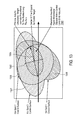
- FIG. 16 a depicts a two dimensional Zernike space. It will be appreciated that embodiments of the invention are not restricted to a two dimensional Zernike space and that the use of two dimensional space merely simplifies illustration of certain aspects of the invention.
- CDs CD 1 . . .
- FIG. 16 b is a graph plotting each of a plurality of Z i curves for one example.
- an ellipse is obtained that covers all CDs and linearization can be obtained by determining the principal axes of the ellipse.
- a cost function for the polynomial in equation (8) may be established as:
- Cost ⁇ ⁇ ⁇ ⁇ L ⁇ CL ⁇ ⁇ ⁇ , ( 10 )
- L ⁇ is a function of all Zernikes.
- This cost function Cost may be minimized using an optimization algorithm.
- the lithometric function L ⁇ is linearized before optimization is attempted.
- nonlinear effects can be handled using alternative methodologies for controlling optimal lens manipulator settings that may include an assumption of no limitations in the photolithographic process. These methodologies can include analyzing the structure of the Zernike subspace reachable by lens manipulator tuning, analyzing the structure of hotspots, determining a cost function and subsequently minimizing the cost function.
- a physical model of a lens manipulator may be used that includes Zernikes that are linearly dependent on the lens manipulator setting, whereby sensitivity is independent of the current lens state.
- Z k Z kh + ⁇ j ⁇ ( S kj * M j ) ( 11 )
- Z k is the after-tuning value of k th Zernike
- Z kh is the raw hot lens value of k th Zernike
- M j is the setting of the j th lens manipulator
- S kj is the sensitivity of the k th Zernike to the j th lens manipulator.
- S kj dZ k /dM j .
- raw hot lens means a lens to which no correction is applied by lens manipulators; i.e., all lens manipulator settings are set at 0.
- the n-dimensional vector ⁇ Z ⁇ obtainable by tuning lens manipulators describes an m-dimensional subspace, which passes through the point ⁇ Z h ⁇ and is expanded by the m column-vectors of ⁇ S ⁇ .
- the lens manipulator setting ⁇ M ⁇ represent the expansion coefficients.
- CD x ( ⁇ M 1 ⁇ ⁇ ... ⁇ ⁇ M m ) ⁇ CD xh + ⁇ ⁇ i ⁇ ( ax i * M i ) + ⁇ ⁇ ij ⁇ ( bx ij * M i * M j ) ( 14 )
- CD xh is the CD x value at raw hot lens
- ax i and bx ij are the coefficients computed for CD x and x lies between 1 and X. Equation (14) maps out the CD variation within the Zernike subspace reachable by tuning the lens manipulators.
- a cost function can be generated and minimized.
- the objectives of lens manipulator optimization typically include minimizing the maximum deviation of each CD x from its corresponding control target:
- a cost function F can be defined:
- the derivative of cost function F for each lens manipulator can be analytically computed by substituting equation (14) into equation (17).
- the resultant equation can then be minimized using a nonlinear minimization method such as the “steepest descent” method to minimize the cost functions F.
- focus F and exposure dose E can be optimized for lens heating.
- the lens manipulators no special assumptions were made for the lens manipulators except that a hotspot CD can be expressed as a second order polynomial of lens manipulator setting.
- the polynomial expansion can further include process window variables focus F and exposure dose E.
- FIG. 3 depicts one example of a lithographic process according to certain aspects of the invention.
- the depicted system describes the use of a model calibrated to data collected from a lens; the data is typically collected while the lens is in a cold state.
- the model can then be combined with additional data to obtain a predictive model that can be used without calibration while the lens is in a heated state.
- a lens model 306 is obtained while the lens is cold.
- the lens model typically characterizes sequences of power and heating 307 in order to obtain throughput models.
- the lens heating models may be validated using measurements obtained through testing and production results.
- a twin scan model 308 described in more detail below, can then be generated and combined to obtain a Lens Heating Focus Exposure Matrix (LH FEM) model 310 M(f,e,x,y) that is based in part on a Focus Exposure Matrix calibration 305 M(f,e) obtained from test patterns 301 and wafer data 303 .
- LH FEM Lens Heating Focus Exposure Matrix
- the LH FEM model 310 is then used for product design 312 used in a plurality of applications 314 including Optical Proximity Correction (OPC), verification, Source Mask Optimization (SMO), Lens Model optimization and lot optimization applications (wherein a lot is a group of substrates to be exposed in the photolithographic process).
- OPC Optical Proximity Correction
- SMO Source Mask Optimization
- Lens Model optimization and lot optimization applications (wherein a lot is a group of substrates to be exposed in the photolithographic process).
- FIG. 4 depicts elements in one example of a product reticle design 312 according to certain aspects of the invention.
- the depicted system describes the use of a model calibrated to data collected from a lens; the data is typically collected while the lens is in a cold state. The model is then combined with additional data to obtain a predictive model that is used without calibration while the lens is in a heated state.
- a lens model 402 is obtained while the lens is cold and one or more other lens models 403 are obtained after the lens has been heated through use.
- the lens models 402 and 403 typically characterize sequences of power and heating in order to obtain throughput models.
- the lens models 402 and 403 are validated using measurements obtained through testing and production results.
- the cold 402 and hot 403 lens models can be used to generate corresponding cold lens contours 404 and hot lens contours 405 . These contours may then be analyzed for hot spots 406 using a cold lens and hot spots 407 using a hot lens. The differences in hotspots may be determined as lens heating induced hotspots 410 and these differences can be used to characterize performance of the lens over a given temperature cycle.
- a cold lens process window 408 may be mapped based on hot spots 406 for one or more reticles and a hot lens process window 409 may be mapped based on hot spots 407 for the same one or more reticles. These process windows 408 and 409 may then be combined 412 to delineate the combined process window covering hot and cold lens operation. At the same time loss of process window may be measured to identify performance enhancements that may be obtained if the state of heating of the lens is changed.
- Lot Optimization is illustrated in FIG. 5 .
- Heating and cooling sequences can be simulated with multiple verification jobs.
- a typical process includes determining a safe number of lots by verifying against a preset metric using process window, CDU, etc., and determining a best choice for the next design/illumination after previous run and calculating any required delay.
- Certain embodiments employ an ASCAL or dynamic lens heating model.
- a steady state lens heating model comprising a physics-based predictive model.
- the model assumes a lens that operates in saturation with maximum field size and numerical aperture.
- the model is slit position dependent.
- an ASCAL-based lens heating model is employed that is based on actual measurements obtained using real patterning devices (such as masks or reticles) on real lithographic exposure apparatuses, for example scanners. This model may be configured to be slit and scan position dependent and is capable of reconstructing dynamic lens behavior.
- Certain embodiments utilize a dynamic lens heating model that can be characterized as a physics-based predictive model.
- the dynamic lens heating model can characterize real-time dynamic lens behavior and may be configured to support flexible field sizes and numerical aperture.
- the model may accommodate for asymmetric patterning means such as reticles.
- the model is flexible and configurable and can be extended to describe different lens configurations and combinations.
- FIGS. 6 a - 6 c depict the relationship of critical dimension errors to slit position, the differences between clip-based models and full-chip models and the relationship between the number of hotspots observed for different ALE configurations.
- FIG. 6 a shows that, for single dimension patterns, clip-based models experience a difference of up to 1 nm critical dimension (CD) error compared to full-chip model.
- FIG. 6 b shows that, for one- and two-dimension patterns, clip-based models grossly over-predict the number of hot spots compared to a full chip model indicating that it is often preferable to employ a full-chip model.
- CD critical dimension
- FIG. 6 c is a chart that depicts the effect of lens heating on the number of detected hotspots.
- the chart is created for the same example of a DRAM device used in FIGS. 6 a and 6 b with different slit positions and lens corrections.
- the differences in lens behavior at different slit positions influences operation of certain embodiments of the invention including matching layout patterns with slit positions to avoid over- or under-predicting hot spots.
- flat full-chip analysis may be used for actual product designs because a conventional hierarchical based analysis approach may not be suitable in all instances. Similar cross slit signatures are observed for different lens corrections and these can be worse at edge position compared with the center position.
- simulation of clip design without a known placement may be performed for multiple slit positions and accommodation made for worst case situations. For example, SMO, Design For Manufacturing (DFM) and other techniques may be employed.
- SMO Design For Manufacturing
- FIG. 7 graphically depicts an example of a lens heating verification process useful in providing a full design, full process window through slit simulation.
- hot spots comprise patterns that are sensitive to lens heating effects such as patterns that pass cold lens model but fail steady state models and large contour deviations between cold and steady state models.
- the process windows include overlapping windows of cold and steady state conditions and may be related to different power settings and different illumination and OPC conditions.
- LMC lens heating verification tool with lithography manufacturability checking
- LMC typically comprises a high accuracy, high speed, high capacity, 100% coverage OPC verification tool.
- LMC applies image-based simulation on full chip design throughout the process window, identifies common catastrophic or yield limiting hot spots such as bridging, necking, CD uniformity error, and multi-layer overlays error and quantifies the total process window.
- the use of a lens heating model allows LMC to locate hot spots by scanning through an entire layout, quantify process window impact due to lens heating effect, and verify corrective measures against such effects.
- FIG. 8 is a block diagram showing an example of a lens heating aware OPC which can operate as a high accuracy, high speed OPC correction tool and which provides dense sampling for best CD uniformity control.
- a process window solver 810 allows multiple models 804 , 805 and process window conditions 808 to guard against catastrophic failures off nominal conditions 806 .
- the OPC may comprise a lens heating model (OPC+) 802 that can account for lens heating effect by applying the steady state models together with cold lens models 803 in other OPC systems.
- OPC are simultaneously optimized for cold and hot lens states across slit across process window and a process window solver can be applied for multiple slit and multiple process window conditions to remove catastrophic pattern failures such as bridging and necking.
- the process solver window 810 can operate to regulate correction algorithms 812 in order to remove PW failures. Correction algorithms 812 can adjust edges to drive down edge placement errors (EPE).
- EPE edge placement errors
- FIG. 9 shows examples of hot spots obtained from simulation that shows results obtained using an uncorrected lens superimposed on corresponding results obtained using a corrected lens.
- FIGS. 14 and 15 illustrate results that can be obtained using systems and methods according to certain aspects of the invention. In particular, FIG. 15 shows a 200%-300% improvement in CDU over conventional lens models.
- results 100 obtained from an OPC system without lens heating awareness show the occurrence of necking (circled) 101 while results 102 from a lens heating aware embodiment is notable for the absence of necking.
- the OPC is optimized for cold lens state and can create necking problems at hot lens state at all slit positions, while in the latter case, lens heating aware OPC does not generate the same necking problems at both cold and hot lens states for all slit positions.
- the image tuner 1102 can account for litho metrics as part of lens manipulator optimization, thereby producing a better solution for reducing litho defects.
- a lens model without image tuner can minimize residual wave fronts 1104 but the results obtained may not represent the optimal solution for minimizing aberration-induced litho defects 1106 , unless aberration can be minimized 1108 until practically non-existent.
- FIG. 12 illustrates application-specific lens heating control using an image tuner.
- Full chip simulation can be useful in optimizing hot spot reduction.
- Litho metric characterization can express a litho metric L as a function of Zernike l i (z i ).
- the litho metric translation component can then translate the litho metric L into Zernike based metric J k (z i ).
- FIG. 13 graphically illustrates litho metrics construction wherein the solution volume is approximated by the maximum inscribed hyper-dimensional ellipsoid 1300 within the control surfaces of individual hotspots 1306 - 1308 .
- the unit vectors of the principal axes 1302 and 1304 may be used as the linearized litho metrics with the weights inversely proportional to the axis lengths.
- results for a 59 nm flash device clip were obtained.
- the clip can be characterized as having dipole source with pole angle of 90 degree and ring width of 0.18, unpolarized source.
- 1401 BALE correction was employed and a lens heating model based on full chip diffraction pattern and reticle transmission was used.
- hot spot selection one dimensional patterns exhibited a deviation from cold lens best condition CD of less than 10 percent.
- Lens heating modeling and verification was conducted with Tachyon FEM and Tachyon LMC with clips placed on both center and edge slit positions. For necking hot spots, simulation of Image Tuner correction may be appreciated with reference to FIGS. 14 and 15 .
- Image tuner correction was found to provide improvement closer to cold lens state and showed slightly bigger through slit variation.
- the disclosed image tuner lens showed a 2-3 times CDU improvement in comparison to a conventional lens model.
- the deviation between cold lens and hot lens models show >10% difference in CD (W 0 case).
- the simulation shows that Image Tuner correction obtained a deviation reduced to ⁇ 10% for all hot spots, for both center and edge slit positions (W 5 case).
- Certain embodiments incorporate lens heating modeling full-chip lithography simulation systems.
- Full-chip verification can be applied to identify lens heating induced hot spots and verify lens heating corrections and lens heating aware OPC can be used to mitigate the lens heating impact on image quality.
- Full-chip simulations can be used to generate application specific recipes to be fed into the Image Tuner, which has the potential of improving imaging performance in the presence of lens heating, as compared to conventional lens models.
- Certain embodiments of the invention provide methods for calibrating a photolithographic system. Some of these embodiments comprise generating a cold lens contour for a reticle design, generating at least one hot lens contour for the reticle design, characterizing aberrations induced by a lens manipulator in a manipulator model and optimizing a process window using the manipulator model, wherein the process window is based on the cold lens contour and the at least one hot lens contour.
- generating a contour includes performing diffraction calculations based on the reticle design.
- the cold lens contour is generated while the lens is maintained within a nominal operating temperature range.
- a hot lens contour is generated after working portions of the lens have been heated by light transmission.
- the manipulation model causes manipulation of a lens of the photolithographic system according to manipulator settings calculated to provide an optimum process window.
- generating the cold lens contour includes using a model based on measurements obtained while the lens is maintained within a nominal operating temperature range.
- each hot lens contour is generated using a corresponding lens heating model, wherein the lens heating model characterizes light-induced heating of the lens in a photolithographic process.
- optimizing the process window includes minimizing variations in critical dimensions caused by lens heating by inducing other variations in critical dimensions caused by lens aberrations.
- the step of characterizing aberrations includes, identifying variations in critical dimensions caused by lens aberrations for a plurality of manipulator settings and modeling behavior of the manipulator as a linear relationship between manipulator settings and aberrations.
- Some of these embodiments further comprise identifying first variations in critical dimensions caused by lens heating.
- characterizing aberrations includes modeling behavior of the manipulator as a linear relationship between manipulator settings and the induced aberrations and identifying second variations in the critical dimensions caused by the induced aberrations for a plurality of manipulator settings.
- the critical dimensions are identified in an image of the reticle.
- the first variations in critical dimensions are expressed as a function of lens heating.
- the second variations in critical dimensions are expressed as a function of manipulator setting.
- the first and second variations in the critical dimensions are expressed as a function of Zernikes.
- Zernike coefficients represent perturbations in the critical dimensions caused by the manipulator.
- Zernikes coefficients characterize the manipulator induced aberrations.
- Zernike coefficients represent perturbations in the critical dimensions caused by lens heating.
- optimizing a process window includes generating a cost function for a set of critical locations. In some of these embodiments, optimizing a process window includes generating a cost function for a set of critical hotspots. In some of these embodiments, wherein optimizing a process window includes minimizing the cost function. In some of these embodiments, minimizing the cost function includes calculating a gradient of the cost function using one of a deepest descent method and a conjugate gradient method.
- Certain embodiments of the invention provide device manufacturing methods for calibrating a photolithographic system. Some of these embodiments comprise (a) providing a substrate that is at least partially covered by a layer of radiation-sensitive material, (b) providing a projection beam of radiation using an imaging system and generating a mask utilized to endow the projection beam with a pattern in its cross-section, and (c) projecting the patterned beam of radiation onto a target portion of the layer of radiation-sensitive material. In some of these embodiments, step (b) comprises generating a cold lens contour for the mask, generating at least one hot lens contour for the mask, characterizing aberrations induced by a lens manipulator in a manipulator model and optimizing a process window using the manipulator model.
- step (c) comprises manipulating a lens of the photolithographic system according to manipulator settings calculated to provide an optimum process window.
- Certain embodiments of the invention provide a computer readable medium bearing a computer program for calibrating a photolithographic system according to the methods recited above.
- the computer program in some of embodiments, when executed, causes a computer to perform the steps of generating a cold lens contour for a reticle design, generating at least one hot lens contour for the reticle design, characterizing aberrations induced by a lens manipulator in a manipulator model, and optimizing a process window using the manipulator model and, in some of these embodiments, the process window is based on the cold lens contour and the at least one hot lens contour.
Abstract
Description
and where mj(j=1,2 . . . ) are lens manipulators, z*i (i=1,2 . . . ) are existing Zernikes, zi (i=1,2 . . . ) are total Zernikes, and sij are sensitivities of the Zernikes z to the lens manipulators m. For a given lithography process, CD variations caused by lens aberrations can be expressed as a function of aberration Zernikes which can be approximated by a quadratic function:
wherein bi and sij are CD variation coefficients. Substituting equation (1), the relationship between CD variations and lens manipulators may be written as:
Given an objective of controlling the lens such that CD variations lie within predefined control limits (e.g., 10% of target CD variations), then
|ΔCDk|≦CLk, (4)
where k (k=1,2,3 . . . ) denotes a set of critical locations or hotspots at which the CDs are measured. This can be formulated as an optimization problem of the following cost function:
in which the goal is to minimize G in manipulator space M.
where q is typically a large even number selected to mimic the behavior of equation (5). This formulation allows the gradient to be calculated analytically and enables fast methods such as steepest descent method, conjugate gradient method, etc.
L α=ƒ(Z i) α=1,2 . . . n (7)
Thus, for a set of CDs (CD1 . . . CDn) printed from a selected mask:
L α=ƒ(Z 1 ,Z 2 . . . Z n) (8)
Objectives of the optimization process include controlling the effects of lens heating such that |ΔLα|<CLα, wherein CLα represents a maximally acceptable value of the lithometric function.
PA B=ƒ(Z 1 . . . Z i) (9)
Thus, an ellipse is obtained that covers all CDs and linearization can be obtained by determining the principal axes of the ellipse.
where the lithometric function Lα is a function of all Zernikes. This cost function Cost may be minimized using an optimization algorithm. Preferably, the Zernikes can be reduced to an expression in the form of Z=ƒ(M), where M is a set comprising one or more manipulator settings (i.e. a plurality of manipulator settings). Consequently, the cost function Cost becomes a function of the plurality of manipulator settings M.
where Zk is the after-tuning value of kth Zernike, Zkh is the raw hot lens value of kth Zernike, Mj is the setting of the jth lens manipulator, Skj is the sensitivity of the kth Zernike to the jth lens manipulator. Skj=dZk/dMj. As used herein, “raw hot lens” means a lens to which no correction is applied by lens manipulators; i.e., all lens manipulator settings are set at 0. Writing (11) in a matrix form:
{Z}={Z h }+{S}*{M} (12)
where {Z} and {Zh} are n-dimensional vectors, {S } is an n-by-m matrix and {M} is an m-dimensional vector.
|(CD x −CD x0)≦CDC x; (13)
i.e., the absolute deviation of CDx from its target CDx0 must not exceed CDCx. Using equation (12), and assuming that {S} is known or is extractable from photolithographic system configuration or programming, then an analytical form can be computed as a polynomial expansion of the dependence of each CD on lens manipulator settings, commencing with a raw hot lens state. Using a 2nd order approximation:
where: CDxh is the CDx value at raw hot lens, axi and bxij are the coefficients computed for CDx and x lies between 1 and X. Equation (14) maps out the CD variation within the Zernike subspace reachable by tuning the lens manipulators.
A cost function F can be defined:
This max-abs cost function can be difficult to minimize because of the non-existence of its derivative and, as an alternative, certain embodiments modify the cost function as follows:
The fourth power is used in the example represented by equation (17) to approximate the max-abs function. The power may be selected arbitrarily and/or based on the nature of the lens, reticle design, past experience, attributes of the photolithographic process and intuition.
Claims (34)
Priority Applications (2)
| Application Number | Priority Date | Filing Date | Title |
|---|---|---|---|
| US12/475,071 US8570485B2 (en) | 2008-06-03 | 2009-05-29 | Lens heating compensation systems and methods |
| US14/064,937 US9746784B2 (en) | 2008-06-03 | 2013-10-28 | Lens heating compensation systems and methods |
Applications Claiming Priority (3)
| Application Number | Priority Date | Filing Date | Title |
|---|---|---|---|
| US5850208P | 2008-06-03 | 2008-06-03 | |
| US12253708P | 2008-12-15 | 2008-12-15 | |
| US12/475,071 US8570485B2 (en) | 2008-06-03 | 2009-05-29 | Lens heating compensation systems and methods |
Related Child Applications (1)
| Application Number | Title | Priority Date | Filing Date |
|---|---|---|---|
| US14/064,937 Continuation US9746784B2 (en) | 2008-06-03 | 2013-10-28 | Lens heating compensation systems and methods |
Publications (2)
| Publication Number | Publication Date |
|---|---|
| US20090296055A1 US20090296055A1 (en) | 2009-12-03 |
| US8570485B2 true US8570485B2 (en) | 2013-10-29 |
Family
ID=41228258
Family Applications (2)
| Application Number | Title | Priority Date | Filing Date |
|---|---|---|---|
| US12/475,071 Active 2031-11-11 US8570485B2 (en) | 2008-06-03 | 2009-05-29 | Lens heating compensation systems and methods |
| US14/064,937 Active 2031-05-07 US9746784B2 (en) | 2008-06-03 | 2013-10-28 | Lens heating compensation systems and methods |
Family Applications After (1)
| Application Number | Title | Priority Date | Filing Date |
|---|---|---|---|
| US14/064,937 Active 2031-05-07 US9746784B2 (en) | 2008-06-03 | 2013-10-28 | Lens heating compensation systems and methods |
Country Status (3)
| Country | Link |
|---|---|
| US (2) | US8570485B2 (en) |
| JP (1) | JP5225463B2 (en) |
| WO (1) | WO2009148976A1 (en) |
Cited By (17)
| Publication number | Priority date | Publication date | Assignee | Title |
|---|---|---|---|---|
| US9218446B1 (en) * | 2014-06-13 | 2015-12-22 | Globalfoundries Inc. | Optimization of integrated circuits for a reticle transmission process window using multiple fill cells |
| US9588438B2 (en) | 2010-11-10 | 2017-03-07 | Asml Netherlands B.V. | Optimization flows of source, mask and projection optics |
| US9940427B2 (en) | 2012-02-09 | 2018-04-10 | Asml Netherlands B.V. | Lens heating aware source mask optimization for advanced lithography |
| US10018922B2 (en) | 2014-09-02 | 2018-07-10 | Nikon Corporation | Tuning of optical projection system to optimize image-edge placement |
| US20180299770A1 (en) * | 2015-10-19 | 2018-10-18 | Asml Netherlands B.V. | Method and apparatus to correct for patterning process error |
| US10345715B2 (en) | 2014-09-02 | 2019-07-09 | Nikon Corporation | Pattern-edge placement predictor and monitor for lithographic exposure tool |
| US10394131B2 (en) | 2015-02-13 | 2019-08-27 | Asml Netherlands B.V. | Image log slope (ILS) optimization |
| US10785394B2 (en) | 2015-08-28 | 2020-09-22 | Kla Corporation | Imaging performance optimization methods for semiconductor wafer inspection |
| US10915689B2 (en) | 2015-10-19 | 2021-02-09 | Asml Netherlands B.V. | Method and apparatus to correct for patterning process error |
| US10948832B2 (en) | 2017-04-06 | 2021-03-16 | Asml Netherlands B.V. | Lithographic method and apparatus |
| US11036146B2 (en) | 2015-10-19 | 2021-06-15 | Asml Netherlands B. V. | Method and apparatus to reduce effects of nonlinear behavior |
| US11529230B2 (en) | 2019-04-05 | 2022-12-20 | Amo Groningen B.V. | Systems and methods for correcting power of an intraocular lens using refractive index writing |
| US11564839B2 (en) | 2019-04-05 | 2023-01-31 | Amo Groningen B.V. | Systems and methods for vergence matching of an intraocular lens with refractive index writing |
| US11583389B2 (en) | 2019-04-05 | 2023-02-21 | Amo Groningen B.V. | Systems and methods for correcting photic phenomenon from an intraocular lens and using refractive index writing |
| US11583388B2 (en) | 2019-04-05 | 2023-02-21 | Amo Groningen B.V. | Systems and methods for spectacle independence using refractive index writing with an intraocular lens |
| US11678975B2 (en) | 2019-04-05 | 2023-06-20 | Amo Groningen B.V. | Systems and methods for treating ocular disease with an intraocular lens and refractive index writing |
| US11944574B2 (en) | 2019-04-05 | 2024-04-02 | Amo Groningen B.V. | Systems and methods for multiple layer intraocular lens and using refractive index writing |
Families Citing this family (40)
| Publication number | Priority date | Publication date | Assignee | Title |
|---|---|---|---|---|
| US7448012B1 (en) | 2004-04-21 | 2008-11-04 | Qi-De Qian | Methods and system for improving integrated circuit layout |
| US9201310B2 (en) * | 2008-08-19 | 2015-12-01 | Asml Netherlands B.V. | Method of measuring overlay error and a device manufacturing method |
| WO2011023214A1 (en) * | 2009-08-31 | 2011-03-03 | Hi-Key Limited | Method for determining the sharpness of a fixed-focus camera, test device for testing the sharpness of a fixed-focus camera, fixed-focus camera as well as method for assembling a fixed-focus camera |
| US8845908B2 (en) | 2010-08-24 | 2014-09-30 | Micron Technology, Inc. | Reticles, and methods of mitigating asymmetric lens heating in photolithography |
| DE102010041528A1 (en) * | 2010-09-28 | 2012-03-29 | Carl Zeiss Smt Gmbh | Projection exposure system with optimized adjustment option |
| NL2007577A (en) * | 2010-11-10 | 2012-05-14 | Asml Netherlands Bv | Optimization of source, mask and projection optics. |
| NL2007579A (en) * | 2010-11-10 | 2012-05-14 | Asml Netherlands Bv | Pattern-dependent proximity matching/tuning including light manipulation by projection optics. |
| KR101529807B1 (en) * | 2011-01-20 | 2015-06-17 | 칼 짜이스 에스엠티 게엠베하 | Method of operating a projection exposure tool |
| US8625078B2 (en) * | 2011-04-06 | 2014-01-07 | Nanya Technology Corp. | Illumination design for lens heating mitigation |
| US8736814B2 (en) | 2011-06-13 | 2014-05-27 | Micron Technology, Inc. | Lithography wave-front control system and method |
| NL2008924A (en) * | 2011-06-22 | 2013-01-02 | Asml Netherlands Bv | System and method to ensure source and image stability. |
| NL2008957A (en) * | 2011-07-08 | 2013-01-09 | Asml Netherlands Bv | Methods and systems for pattern design with tailored response to wavefront aberration. |
| US8609302B2 (en) | 2011-08-22 | 2013-12-17 | Micron Technology, Inc. | Lithography methods, methods for forming patterning tools and patterning tools |
| US9182289B2 (en) * | 2011-10-14 | 2015-11-10 | Canon Kabushiki Kaisha | Apparatus and method for estimating wavefront parameters |
| US8822104B2 (en) | 2011-12-16 | 2014-09-02 | Nanya Technology Corporation | Photomask |
| NL2009982A (en) * | 2012-01-10 | 2013-07-15 | Asml Netherlands Bv | Source mask optimization to reduce stochastic effects. |
| WO2013164187A1 (en) * | 2012-05-04 | 2013-11-07 | Asml Netherlands B.V. | Design rule and lithographic process co-optimization |
| JP6039932B2 (en) * | 2012-06-22 | 2016-12-07 | キヤノン株式会社 | Exposure apparatus, exposure method, and article manufacturing method |
| JP6147924B2 (en) * | 2013-09-14 | 2017-06-14 | カール・ツァイス・エスエムティー・ゲーエムベーハー | Method for operating a microlithographic projection apparatus |
| KR102427139B1 (en) * | 2014-02-12 | 2022-07-29 | 에이에스엠엘 네델란즈 비.브이. | Method of optimizing a process window |
| US10025201B2 (en) | 2014-04-14 | 2018-07-17 | Asml Netherlands B.V. | Flows of optimization for lithographic processes |
| US9235677B1 (en) | 2014-07-17 | 2016-01-12 | United Microelectronics Corp. | Thermal uniformity compensating method and apparatus |
| US10866523B2 (en) * | 2015-06-16 | 2020-12-15 | Asml Netherlands B.V. | Process window tracker |
| CN105093857B (en) * | 2015-07-22 | 2017-06-27 | 上海华力微电子有限公司 | The method that serialgram isolated wafer line width declines under solution high-energy |
| TWI625460B (en) * | 2016-05-20 | 2018-06-01 | 國立臺南大學 | Enhanced geothermal system and method for building such system |
| US10121709B2 (en) * | 2017-01-24 | 2018-11-06 | Lam Research Corporation | Virtual metrology systems and methods for using feedforward critical dimension data to predict other critical dimensions of a wafer |
| CN110546575B (en) * | 2017-04-26 | 2021-10-22 | Asml荷兰有限公司 | Device manufacturing method |
| CN107092145A (en) * | 2017-06-19 | 2017-08-25 | 武汉华星光电技术有限公司 | The manufacture method of low temperature polycrystalline silicon array base palte |
| EP3495888A1 (en) | 2017-12-06 | 2019-06-12 | ASML Netherlands B.V. | Method for controlling a lithographic apparatus and associated apparatuses |
| KR20230065371A (en) * | 2018-06-25 | 2023-05-11 | 에이에스엠엘 네델란즈 비.브이. | Wavefront optimization for tuning scanner based on performance matching |
| TWI794544B (en) * | 2018-10-09 | 2023-03-01 | 荷蘭商Asml荷蘭公司 | Method for high numerical aperture thru-slit source mask optimization |
| KR20200043767A (en) | 2018-10-18 | 2020-04-28 | 삼성전자주식회사 | EUV(Extreme Ultra-Violet) exposure apparatus and exposure method, and method for fabricating semiconductor device comprising the exposure method |
| EP3702839B1 (en) * | 2019-02-27 | 2021-11-10 | ASML Netherlands B.V. | Method of reducing effects of lens heating and/or cooling in a lithographic process |
| WO2020193010A1 (en) | 2019-03-22 | 2020-10-01 | Asml Netherlands B.V. | Method for controlling a lithographic apparatus and associated apparatuses |
| EP3764164A1 (en) | 2019-07-11 | 2021-01-13 | ASML Netherlands B.V. | Method for controlling a lithographic apparatus and associated apparatuses |
| CN115066657A (en) | 2020-02-12 | 2022-09-16 | Asml荷兰有限公司 | Method and associated apparatus for controlling a manufacturing process |
| WO2022002519A1 (en) * | 2020-07-01 | 2022-01-06 | Asml Netherlands B.V. | Method for thermo-mechanical control of a heat sensitive element and device for use in a lithographic production process |
| DE102021211975A1 (en) | 2021-10-25 | 2023-04-27 | Carl Zeiss Smt Gmbh | Method for simulating a target wavefront of an imaging optical production system and metrology system for carrying out the method |
| DE102021213827A1 (en) | 2021-12-06 | 2023-06-07 | Carl Zeiss Smt Gmbh | Method for optimizing a pupil diaphragm shape for simulating lighting and imaging properties of an optical production system when illuminating and imaging an object using an optical measuring system |
| DE102023208870A1 (en) * | 2022-09-23 | 2024-03-28 | Carl Zeiss Smt Gmbh | Method for operating a projection exposure system |
Citations (15)
| Publication number | Priority date | Publication date | Assignee | Title |
|---|---|---|---|---|
| JPH06326000A (en) | 1993-05-14 | 1994-11-25 | Canon Inc | Projection aligner |
| US5969441A (en) | 1996-12-24 | 1999-10-19 | Asm Lithography Bv | Two-dimensionally balanced positioning device with two object holders, and lithographic device provided with such a positioning device |
| US6046792A (en) | 1996-03-06 | 2000-04-04 | U.S. Philips Corporation | Differential interferometer system and lithographic step-and-scan apparatus provided with such a system |
| JP2001230193A (en) | 2000-02-18 | 2001-08-24 | Canon Inc | Wave front aberration measuring method and projection aligner |
| JP2001244182A (en) | 2000-02-29 | 2001-09-07 | Canon Inc | Method of measuring variations in image formation characteristics of projection optical system due to exposure heat and aligner |
| US20020036758A1 (en) | 2000-06-14 | 2002-03-28 | Asml Netherlands Bv | Method of operating an optical imaging system, lithographic projection apparatus, device manufacturing method, and device manufactured thereby |
| US6578190B2 (en) * | 2001-01-11 | 2003-06-10 | International Business Machines Corporation | Process window based optical proximity correction of lithographic images |
| US20040184030A1 (en) * | 2002-11-12 | 2004-09-23 | Armin Liebchen | Method and apparatus for providing lens aberration compensation by illumination source optimization |
| US20050136340A1 (en) * | 2000-07-21 | 2005-06-23 | Asml Netherlands B.V. | Lithographic apparatus and methods, patterning structure and method for making a patterning structure, device manufacturing method, and device manufactured thereby |
| US20060008716A1 (en) | 2004-07-08 | 2006-01-12 | Asml Netherlands B.V. | Lithographic projection apparatus and a device manufacturing method using such lithographic projection apparatus |
| US7003758B2 (en) | 2003-10-07 | 2006-02-21 | Brion Technologies, Inc. | System and method for lithography simulation |
| US20060114437A1 (en) | 2004-12-01 | 2006-06-01 | Asml Netherlands B.V. | Lithographic projection apparatus and device manufacturing method using such lithographic projection apparatus |
| JP2006179937A (en) | 2004-12-23 | 2006-07-06 | Asml Netherlands Bv | Lithographic equipment, excimer laser, and device manufacturing method |
| US20080086440A1 (en) * | 2006-10-06 | 2008-04-10 | Nikon Precision Inc. | Automated signature detection system and method of use |
| US20080097701A1 (en) * | 2006-09-07 | 2008-04-24 | Mcgill University | Short term and long term forecasting systems with enhanced prediction accuracy |
Family Cites Families (3)
| Publication number | Priority date | Publication date | Assignee | Title |
|---|---|---|---|---|
| US6791666B2 (en) * | 2001-11-19 | 2004-09-14 | Taiwan Semiconductor Manufacturing Co., Ltd | Variable transmission focal mask for lens heating compensation |
| KR101056142B1 (en) * | 2004-01-29 | 2011-08-10 | 케이엘에이-텐코 코포레이션 | Computerized method for detecting defects in reticle design data |
| WO2007030704A2 (en) | 2005-09-09 | 2007-03-15 | Brion Technologies, Inc. | System and method for mask verification using an individual mask error model |
-
2009
- 2009-05-29 JP JP2011512551A patent/JP5225463B2/en active Active
- 2009-05-29 WO PCT/US2009/045732 patent/WO2009148976A1/en active Application Filing
- 2009-05-29 US US12/475,071 patent/US8570485B2/en active Active
-
2013
- 2013-10-28 US US14/064,937 patent/US9746784B2/en active Active
Patent Citations (18)
| Publication number | Priority date | Publication date | Assignee | Title |
|---|---|---|---|---|
| JPH06326000A (en) | 1993-05-14 | 1994-11-25 | Canon Inc | Projection aligner |
| US6046792A (en) | 1996-03-06 | 2000-04-04 | U.S. Philips Corporation | Differential interferometer system and lithographic step-and-scan apparatus provided with such a system |
| US5969441A (en) | 1996-12-24 | 1999-10-19 | Asm Lithography Bv | Two-dimensionally balanced positioning device with two object holders, and lithographic device provided with such a positioning device |
| JP2001230193A (en) | 2000-02-18 | 2001-08-24 | Canon Inc | Wave front aberration measuring method and projection aligner |
| JP2001244182A (en) | 2000-02-29 | 2001-09-07 | Canon Inc | Method of measuring variations in image formation characteristics of projection optical system due to exposure heat and aligner |
| US20020036758A1 (en) | 2000-06-14 | 2002-03-28 | Asml Netherlands Bv | Method of operating an optical imaging system, lithographic projection apparatus, device manufacturing method, and device manufactured thereby |
| US20050136340A1 (en) * | 2000-07-21 | 2005-06-23 | Asml Netherlands B.V. | Lithographic apparatus and methods, patterning structure and method for making a patterning structure, device manufacturing method, and device manufactured thereby |
| US6578190B2 (en) * | 2001-01-11 | 2003-06-10 | International Business Machines Corporation | Process window based optical proximity correction of lithographic images |
| US20040184030A1 (en) * | 2002-11-12 | 2004-09-23 | Armin Liebchen | Method and apparatus for providing lens aberration compensation by illumination source optimization |
| US7003758B2 (en) | 2003-10-07 | 2006-02-21 | Brion Technologies, Inc. | System and method for lithography simulation |
| US20060008716A1 (en) | 2004-07-08 | 2006-01-12 | Asml Netherlands B.V. | Lithographic projection apparatus and a device manufacturing method using such lithographic projection apparatus |
| JP2006024941A (en) | 2004-07-08 | 2006-01-26 | Asml Netherlands Bv | Lithography projection equipment and device manufacturing method using the lithography projection equipment |
| US20060114437A1 (en) | 2004-12-01 | 2006-06-01 | Asml Netherlands B.V. | Lithographic projection apparatus and device manufacturing method using such lithographic projection apparatus |
| JP2006179937A (en) | 2004-12-23 | 2006-07-06 | Asml Netherlands Bv | Lithographic equipment, excimer laser, and device manufacturing method |
| US20060170899A1 (en) | 2004-12-23 | 2006-08-03 | Asml Netherlands B.V. | Lithographic apparatus, excimer laser and device manufacturing method |
| US7817247B2 (en) | 2004-12-23 | 2010-10-19 | Asml Netherlands B.V. | Lithographic apparatus, excimer laser and device manufacturing method |
| US20080097701A1 (en) * | 2006-09-07 | 2008-04-24 | Mcgill University | Short term and long term forecasting systems with enhanced prediction accuracy |
| US20080086440A1 (en) * | 2006-10-06 | 2008-04-10 | Nikon Precision Inc. | Automated signature detection system and method of use |
Non-Patent Citations (7)
| Title |
|---|
| Cao, et al., "Optimized Hardware and Software for Fast, Full Chip Simulation" , Proc. SPIE, vol. 5754, p. 405, 2005. |
| Granik, et al., "Source Optimization for Image Fidelity and Throughput", J. of Microlithography, Microfabrication+, Microsystems, vol. 3, No. 4, pp. 509-522, 2004. |
| Ichiro Mod et al., "Special Reports/Challenges and Innovations of Advanced Lithography," Toshiba Review, vol. 59, No. 8, pp. 8-12 (2004). |
| International Search Report issued Nov. 24, 2009 in corresponding PCT/US09/045732. |
| Japanese Office Action mailed Jun. 19, 2012 in corresponding Japanese Patent Application No. 2011-512551. |
| Rosenbluth, et al., "Optimum Mask and Source Patterns to Print a Given Shape", Journal of Microlithography, Microfabrication, Microsystems, vol. 1, No. 1, pp. 13-20, 2002. |
| Spence, et al. , "Full Chip Lithography Simulation and Design Analysis-How OPC is Changing IC Design", Proc. SPIE, vol. 5751, pp. 1-14, 2005. |
Cited By (20)
| Publication number | Priority date | Publication date | Assignee | Title |
|---|---|---|---|---|
| US9588438B2 (en) | 2010-11-10 | 2017-03-07 | Asml Netherlands B.V. | Optimization flows of source, mask and projection optics |
| US10401732B2 (en) | 2010-11-10 | 2019-09-03 | Asml Netherlands B.V. | Optimization flows of source, mask and projection optics |
| US9940427B2 (en) | 2012-02-09 | 2018-04-10 | Asml Netherlands B.V. | Lens heating aware source mask optimization for advanced lithography |
| US9218446B1 (en) * | 2014-06-13 | 2015-12-22 | Globalfoundries Inc. | Optimization of integrated circuits for a reticle transmission process window using multiple fill cells |
| US10018922B2 (en) | 2014-09-02 | 2018-07-10 | Nikon Corporation | Tuning of optical projection system to optimize image-edge placement |
| US10345715B2 (en) | 2014-09-02 | 2019-07-09 | Nikon Corporation | Pattern-edge placement predictor and monitor for lithographic exposure tool |
| US10488763B2 (en) | 2014-09-02 | 2019-11-26 | Nikon Corporation | Pattern-edge placement predictor and monitor for lithographic exposure tool |
| US10394131B2 (en) | 2015-02-13 | 2019-08-27 | Asml Netherlands B.V. | Image log slope (ILS) optimization |
| US10785394B2 (en) | 2015-08-28 | 2020-09-22 | Kla Corporation | Imaging performance optimization methods for semiconductor wafer inspection |
| US10915689B2 (en) | 2015-10-19 | 2021-02-09 | Asml Netherlands B.V. | Method and apparatus to correct for patterning process error |
| US20180299770A1 (en) * | 2015-10-19 | 2018-10-18 | Asml Netherlands B.V. | Method and apparatus to correct for patterning process error |
| US11036146B2 (en) | 2015-10-19 | 2021-06-15 | Asml Netherlands B. V. | Method and apparatus to reduce effects of nonlinear behavior |
| US10948832B2 (en) | 2017-04-06 | 2021-03-16 | Asml Netherlands B.V. | Lithographic method and apparatus |
| US11529230B2 (en) | 2019-04-05 | 2022-12-20 | Amo Groningen B.V. | Systems and methods for correcting power of an intraocular lens using refractive index writing |
| US11564839B2 (en) | 2019-04-05 | 2023-01-31 | Amo Groningen B.V. | Systems and methods for vergence matching of an intraocular lens with refractive index writing |
| US11583389B2 (en) | 2019-04-05 | 2023-02-21 | Amo Groningen B.V. | Systems and methods for correcting photic phenomenon from an intraocular lens and using refractive index writing |
| US11583388B2 (en) | 2019-04-05 | 2023-02-21 | Amo Groningen B.V. | Systems and methods for spectacle independence using refractive index writing with an intraocular lens |
| US11678975B2 (en) | 2019-04-05 | 2023-06-20 | Amo Groningen B.V. | Systems and methods for treating ocular disease with an intraocular lens and refractive index writing |
| US11931296B2 (en) | 2019-04-05 | 2024-03-19 | Amo Groningen B.V. | Systems and methods for vergence matching of an intraocular lens with refractive index writing |
| US11944574B2 (en) | 2019-04-05 | 2024-04-02 | Amo Groningen B.V. | Systems and methods for multiple layer intraocular lens and using refractive index writing |
Also Published As
| Publication number | Publication date |
|---|---|
| WO2009148976A1 (en) | 2009-12-10 |
| JP5225463B2 (en) | 2013-07-03 |
| US20090296055A1 (en) | 2009-12-03 |
| JP2011522441A (en) | 2011-07-28 |
| US20140047397A1 (en) | 2014-02-13 |
| US9746784B2 (en) | 2017-08-29 |
Similar Documents
| Publication | Publication Date | Title |
|---|---|---|
| US9746784B2 (en) | Lens heating compensation systems and methods | |
| TWI502286B (en) | Lens heating aware source mask optimization for advanced lithography | |
| US9390206B2 (en) | Methods and systems for lithography process window simulation | |
| US9934350B2 (en) | Pattern selection for full-chip source and mask optimization | |
| US8542340B2 (en) | Illumination optimization | |
| US9009647B2 (en) | Methods and systems for lithography calibration using a mathematical model for a lithographic process | |
| US10712653B2 (en) | Etch variation tolerant optimization | |
| US20170176864A1 (en) | Optimization flows of source, mask and projection optics | |
| TWI460547B (en) | Model-based process simulation systems and methods | |
| KR20120050390A (en) | Pattern-dependent proximity matching/tuning including light manipulation by projection optics | |
| TWI615684B (en) | Profile aware source-mask optimization | |
| US9965578B2 (en) | Compensation for patterning device deformation | |
| KR20180011263A (en) | Simulation of lithography using multi-sampling of angular distribution of source radiation |
Legal Events
| Date | Code | Title | Description |
|---|---|---|---|
| AS | Assignment |
Owner name: BRION TECHNOLOGIES, INC., CALIFORNIA Free format text: ASSIGNMENT OF ASSIGNORS INTEREST;ASSIGNORS:YE, JUN;LIU, PENG;CAO, YU;SIGNING DATES FROM 20090714 TO 20090715;REEL/FRAME:022979/0120 |
|
| AS | Assignment |
Owner name: ASML NETHERLANDS B.V.,NETHERLANDS Free format text: ASSIGNMENT OF ASSIGNORS INTEREST;ASSIGNOR:BRION TECHNOLOGIES, INC.;REEL/FRAME:024278/0346 Effective date: 20100416 Owner name: ASML NETHERLANDS B.V., NETHERLANDS Free format text: ASSIGNMENT OF ASSIGNORS INTEREST;ASSIGNOR:BRION TECHNOLOGIES, INC.;REEL/FRAME:024278/0346 Effective date: 20100416 |
|
| STCF | Information on status: patent grant |
Free format text: PATENTED CASE |
|
| FEPP | Fee payment procedure |
Free format text: PAYOR NUMBER ASSIGNED (ORIGINAL EVENT CODE: ASPN); ENTITY STATUS OF PATENT OWNER: LARGE ENTITY |
|
| FPAY | Fee payment |
Year of fee payment: 4 |
|
| MAFP | Maintenance fee payment |
Free format text: PAYMENT OF MAINTENANCE FEE, 8TH YEAR, LARGE ENTITY (ORIGINAL EVENT CODE: M1552); ENTITY STATUS OF PATENT OWNER: LARGE ENTITY Year of fee payment: 8 |