US8580399B2 - Substituted oligoazacarbazoles for light emitting diodes - Google Patents
Substituted oligoazacarbazoles for light emitting diodes Download PDFInfo
- Publication number
- US8580399B2 US8580399B2 US13/082,914 US201113082914A US8580399B2 US 8580399 B2 US8580399 B2 US 8580399B2 US 201113082914 A US201113082914 A US 201113082914A US 8580399 B2 US8580399 B2 US 8580399B2
- Authority
- US
- United States
- Prior art keywords
- group
- compound
- formula
- organic layer
- layer
- Prior art date
- Legal status (The legal status is an assumption and is not a legal conclusion. Google has not performed a legal analysis and makes no representation as to the accuracy of the status listed.)
- Active, expires
Links
- 0 *B(C)C.*BC.*BC([2H])C.*BCC.*BC[2H]C Chemical compound *B(C)C.*BC.*BC([2H])C.*BCC.*BC[2H]C 0.000 description 13
- SDFLTYHTFPTIGX-UHFFFAOYSA-N CN1C2=CC=CC=C2C2=C1/C=C\C=C/2 Chemical compound CN1C2=CC=CC=C2C2=C1/C=C\C=C/2 SDFLTYHTFPTIGX-UHFFFAOYSA-N 0.000 description 4
- VFUDMQLBKNMONU-UHFFFAOYSA-N C1=CC2=C(C=C1)N(C1=CC=C(C3=CC=C(N4C5=C(C=CC=C5)C5=C4/C=C\C=C/5)C=C3)C=C1)C1=C2C=CC=C1 Chemical compound C1=CC2=C(C=C1)N(C1=CC=C(C3=CC=C(N4C5=C(C=CC=C5)C5=C4/C=C\C=C/5)C=C3)C=C1)C1=C2C=CC=C1 VFUDMQLBKNMONU-UHFFFAOYSA-N 0.000 description 3
- GEQBRULPNIVQPP-UHFFFAOYSA-N C1=CC=C(N2C(C3=CC(/C4=N/C5=C(C=CC=C5)N4C4=CC=CC=C4)=CC(/C4=N/C5=C(C=CC=C5)N4C4=CC=CC=C4)=C3)=NC3=C2C=CC=C3)C=C1 Chemical compound C1=CC=C(N2C(C3=CC(/C4=N/C5=C(C=CC=C5)N4C4=CC=CC=C4)=CC(/C4=N/C5=C(C=CC=C5)N4C4=CC=CC=C4)=C3)=NC3=C2C=CC=C3)C=C1 GEQBRULPNIVQPP-UHFFFAOYSA-N 0.000 description 3
- GQTPJTXBRQADGB-UHFFFAOYSA-N C1=CC=C2C(=C1)C1=C(C=CC=C1)C1=C2C=CC=C1.C1=CC=C2C(=C1)C1=C(C=CC=C1)C1=C2C=CC=N1.C1=CC=C2C(=C1)C=CC1=C2C=CC=C1.C1=CC=C2C=CC=CC2=C1.C1=CC=C2N=CC=CC2=C1.C1=CC=CC=C1.C1=CC=NC=C1.C1=CN=CN=C1.C1=NC=NC=N1.CC.CC.CC.CC.CC.CC.CC.CC.CC.CC.CC.CC.CC.CC.CC.CC.CC.CC Chemical compound C1=CC=C2C(=C1)C1=C(C=CC=C1)C1=C2C=CC=C1.C1=CC=C2C(=C1)C1=C(C=CC=C1)C1=C2C=CC=N1.C1=CC=C2C(=C1)C=CC1=C2C=CC=C1.C1=CC=C2C=CC=CC2=C1.C1=CC=C2N=CC=CC2=C1.C1=CC=CC=C1.C1=CC=NC=C1.C1=CN=CN=C1.C1=NC=NC=N1.CC.CC.CC.CC.CC.CC.CC.CC.CC.CC.CC.CC.CC.CC.CC.CC.CC.CC GQTPJTXBRQADGB-UHFFFAOYSA-N 0.000 description 3
- VLKZOEOYAKHREP-UHFFFAOYSA-N CCCCCC Chemical compound CCCCCC VLKZOEOYAKHREP-UHFFFAOYSA-N 0.000 description 3
- FEEVDOPOKYHDKB-UHFFFAOYSA-N C1=CC(C2=C/C3=C(\C=C/2)C2=C(C=CC=C2)C2=C3C=CC=C2)=CC(C2=CC3=C(C=C2)C2=C(C=CC=C2)C2=C3C=CC=C2)=C1 Chemical compound C1=CC(C2=C/C3=C(\C=C/2)C2=C(C=CC=C2)C2=C3C=CC=C2)=CC(C2=CC3=C(C=C2)C2=C(C=CC=C2)C2=C3C=CC=C2)=C1 FEEVDOPOKYHDKB-UHFFFAOYSA-N 0.000 description 2
- HBIDPMHHAZBGDI-UHFFFAOYSA-N C1=CC(C2=CC3=C(C=C2)OC2=C3C=CC=C2)=CC(C2=CC=CC(N3C4=C(C=CC=C4)C4=C3C=CC(N3C5=C(C=CC=C5)C5=C3N=CC=C5)=C4)=C2)=C1.C1=CC(C2=CC3=C(C=C2)SC2=C3C=CC=C2)=CC(C2=CC=CC(N3C4=C(C=CC=C4)C4=C3C=CC(N3C5=C(C=CC=C5)C5=C3N=CC=C5)=C4)=C2)=C1.C1=CC(C2=CC=C3C(=C2)SC2=C3C=CC=C2)=CC(C2=CC=CC(N3C4=C(C=CC=C4)C4=C3C=CC(N3C5=C(C=CC=C5)C5=C3N=CC=C5)=C4)=C2)=C1.C1=CC=C(C2=NC(N3C4=C(C=CC=C4)C4=C3C=CC(N3C5=C(C=CC=C5)C5=C3N=CC=C5)=C4)=CC(C3=CC=CC(C4=CC=CC5=C4SC4=C5C=CC=C4)=C3)=C2)C=C1 Chemical compound C1=CC(C2=CC3=C(C=C2)OC2=C3C=CC=C2)=CC(C2=CC=CC(N3C4=C(C=CC=C4)C4=C3C=CC(N3C5=C(C=CC=C5)C5=C3N=CC=C5)=C4)=C2)=C1.C1=CC(C2=CC3=C(C=C2)SC2=C3C=CC=C2)=CC(C2=CC=CC(N3C4=C(C=CC=C4)C4=C3C=CC(N3C5=C(C=CC=C5)C5=C3N=CC=C5)=C4)=C2)=C1.C1=CC(C2=CC=C3C(=C2)SC2=C3C=CC=C2)=CC(C2=CC=CC(N3C4=C(C=CC=C4)C4=C3C=CC(N3C5=C(C=CC=C5)C5=C3N=CC=C5)=C4)=C2)=C1.C1=CC=C(C2=NC(N3C4=C(C=CC=C4)C4=C3C=CC(N3C5=C(C=CC=C5)C5=C3N=CC=C5)=C4)=CC(C3=CC=CC(C4=CC=CC5=C4SC4=C5C=CC=C4)=C3)=C2)C=C1 HBIDPMHHAZBGDI-UHFFFAOYSA-N 0.000 description 2
- PKNBTVHCQNZQLY-UHFFFAOYSA-N C1=CC(C2=CC=CC(C3=CC=CC4=C3SC3=C4C=CC=C3)=C2)=CC(C2=CC=CC(N3C4=C(C=CC=C4)C4=C3C=CC(N3C5=C(C=CC=C5)C5=C3N=CC=C5)=C4)=C2)=C1.C1=CC(C2=CC=CC3=C2C2=C(C=CC=C2)O3)=CC(C2=CC=CC(N3C4=C(C=CC=C4)C4=C3C=CC(N3C5=C(C=CC=C5)C5=C3N=CC=C5)=C4)=C2)=C1.C1=CC(C2=CC=CC3=C2C2=C(C=CC=C2)S3)=CC(C2=CC=CC(N3C4=C(C=CC=C4)C4=C3C=CC(N3C5=C(C=CC=C5)C5=C3N=CC=C5)=C4)=C2)=C1.C1=CC(C2=CC=CC3=C2SC2=C3C=CC=C2)=CC(C2=CC=CC(N3C4=C(C=C(N5C6=C(C=CC=C6)C6=C5N=CC=C6)C=C4)C4=C3N=CC=C4)=C2)=C1 Chemical compound C1=CC(C2=CC=CC(C3=CC=CC4=C3SC3=C4C=CC=C3)=C2)=CC(C2=CC=CC(N3C4=C(C=CC=C4)C4=C3C=CC(N3C5=C(C=CC=C5)C5=C3N=CC=C5)=C4)=C2)=C1.C1=CC(C2=CC=CC3=C2C2=C(C=CC=C2)O3)=CC(C2=CC=CC(N3C4=C(C=CC=C4)C4=C3C=CC(N3C5=C(C=CC=C5)C5=C3N=CC=C5)=C4)=C2)=C1.C1=CC(C2=CC=CC3=C2C2=C(C=CC=C2)S3)=CC(C2=CC=CC(N3C4=C(C=CC=C4)C4=C3C=CC(N3C5=C(C=CC=C5)C5=C3N=CC=C5)=C4)=C2)=C1.C1=CC(C2=CC=CC3=C2SC2=C3C=CC=C2)=CC(C2=CC=CC(N3C4=C(C=C(N5C6=C(C=CC=C6)C6=C5N=CC=C6)C=C4)C4=C3N=CC=C4)=C2)=C1 PKNBTVHCQNZQLY-UHFFFAOYSA-N 0.000 description 2
- OMUNARCKXCUFRT-UHFFFAOYSA-N C1=CC(C2=CC=CC3=C2OC2=C3C=CC=C2)=CC(C2=CC=CC(N3C4=C(C=CC=C4)C4=C3/C=C\C(N3C5=C(C=CC=C5)C5=C3N=CC=C5)=C/4)=C2)=C1.C1=CC(C2=CC=CC3=C2SC2=C3C=CC=C2)=CC(C2=CC=CC(N3C4=C(C=C(N5C6=C(C=C(N7C8=C(C=C(N9C%10=C(C=CC=C%10)C%10=C9N=CC=C%10)C=C8)C8=C7N=CC=C8)C=C6)C6=C5N=CC=C6)C=C4)C4=C3N=CC=C4)=C2)=C1.C1=CC(C2=CC=CC3=C2SC2=C3C=CC=C2)=CC(C2=CC=CC(N3C4=C(C=C(N5C6=C(C=CC=C6)C6=C5C=NC=C6)C=C4)C4=C3N=CC(N3C5=C(C=CC=C5)C5=C3N=CC=C5)=C4)=C2)=C1 Chemical compound C1=CC(C2=CC=CC3=C2OC2=C3C=CC=C2)=CC(C2=CC=CC(N3C4=C(C=CC=C4)C4=C3/C=C\C(N3C5=C(C=CC=C5)C5=C3N=CC=C5)=C/4)=C2)=C1.C1=CC(C2=CC=CC3=C2SC2=C3C=CC=C2)=CC(C2=CC=CC(N3C4=C(C=C(N5C6=C(C=C(N7C8=C(C=C(N9C%10=C(C=CC=C%10)C%10=C9N=CC=C%10)C=C8)C8=C7N=CC=C8)C=C6)C6=C5N=CC=C6)C=C4)C4=C3N=CC=C4)=C2)=C1.C1=CC(C2=CC=CC3=C2SC2=C3C=CC=C2)=CC(C2=CC=CC(N3C4=C(C=C(N5C6=C(C=CC=C6)C6=C5C=NC=C6)C=C4)C4=C3N=CC(N3C5=C(C=CC=C5)C5=C3N=CC=C5)=C4)=C2)=C1 OMUNARCKXCUFRT-UHFFFAOYSA-N 0.000 description 2
- UEMAJTHLXSFTIN-UHFFFAOYSA-N C1=CC(C2=CC=CC3=C2SC2=C3C=CC=C2)=CC(C2=CC=CC(N3C4=C(C=C(C5=C/C=C/C6=C\5OC5=C6C=CC=C5)C=C4)C4=C3C=CC(N3C5=C(C=CC=C5)C5=C3N=CC=C5)=C4)=C2)=C1.C1=CC(C2=CC=CC3=C2SC2=C3C=CC=C2)=CC(C2=CC=CC(N3C4=C(C=CC=C4)C4=C3C=CC(N3C5=C(C=C(/C6=C/C=C\C7=C6SC6=C7C=CC=C6)C=C5)C5=C3N=CC=C5)=C4)=C2)=C1.C1=CC(C2=CC=CC3=C2SC2=C3C=CC=C2)=CC(C2=CC=CC(N3C4=C(C=CC=C4)C4=C3C=CC(N3C5=C(C=CC=C5)C5=C3N=CC(C3=CC=CC6=C3SC3=C6C=CC=C3)=C5)=C4)=C2)=C1 Chemical compound C1=CC(C2=CC=CC3=C2SC2=C3C=CC=C2)=CC(C2=CC=CC(N3C4=C(C=C(C5=C/C=C/C6=C\5OC5=C6C=CC=C5)C=C4)C4=C3C=CC(N3C5=C(C=CC=C5)C5=C3N=CC=C5)=C4)=C2)=C1.C1=CC(C2=CC=CC3=C2SC2=C3C=CC=C2)=CC(C2=CC=CC(N3C4=C(C=CC=C4)C4=C3C=CC(N3C5=C(C=C(/C6=C/C=C\C7=C6SC6=C7C=CC=C6)C=C5)C5=C3N=CC=C5)=C4)=C2)=C1.C1=CC(C2=CC=CC3=C2SC2=C3C=CC=C2)=CC(C2=CC=CC(N3C4=C(C=CC=C4)C4=C3C=CC(N3C5=C(C=CC=C5)C5=C3N=CC(C3=CC=CC6=C3SC3=C6C=CC=C3)=C5)=C4)=C2)=C1 UEMAJTHLXSFTIN-UHFFFAOYSA-N 0.000 description 2
- QGHKAPWTYFNGNJ-UHFFFAOYSA-N C1=CC(C2=CC=CC3=C2SC2=C3C=CC=C2)=CC(C2=CC=CC(N3C4=C(C=C(N5C6=C(C=C(N7C8=C(C=CC=C8)C8=C7N=CC=C8)C=C6)C6=C5N=CC=C6)C=C4)C4=C3N=CC=C4)=C2)=C1.C1=CC(C2=CC=CC3=C2SC2=C3C=CC=C2)=CC(C2=CC=CC(N3C4=C(C=C(N5C6=C(C=CC=C6)C6=C5N=CC=C6)C=C4)C4=C3N=CC(N3C5=C(C=CC=C5)C5=C3C=CC=N5)=C4)=C2)=C1.C1=CC(C2=CC=CC3=C2SC2=C3C=CC=C2)=CC(C2=CC=CC(N3C4=C(C=C(N5C6=C(C=CC=C6)C6=C5N=CC=C6)C=C4)C4=C3N=CC(N3C5=C(C=CC=C5)C5=C3N=CC=C5)=C4)=C2)=C1 Chemical compound C1=CC(C2=CC=CC3=C2SC2=C3C=CC=C2)=CC(C2=CC=CC(N3C4=C(C=C(N5C6=C(C=C(N7C8=C(C=CC=C8)C8=C7N=CC=C8)C=C6)C6=C5N=CC=C6)C=C4)C4=C3N=CC=C4)=C2)=C1.C1=CC(C2=CC=CC3=C2SC2=C3C=CC=C2)=CC(C2=CC=CC(N3C4=C(C=C(N5C6=C(C=CC=C6)C6=C5N=CC=C6)C=C4)C4=C3N=CC(N3C5=C(C=CC=C5)C5=C3C=CC=N5)=C4)=C2)=C1.C1=CC(C2=CC=CC3=C2SC2=C3C=CC=C2)=CC(C2=CC=CC(N3C4=C(C=C(N5C6=C(C=CC=C6)C6=C5N=CC=C6)C=C4)C4=C3N=CC(N3C5=C(C=CC=C5)C5=C3N=CC=C5)=C4)=C2)=C1 QGHKAPWTYFNGNJ-UHFFFAOYSA-N 0.000 description 2
- TVFIBINKSMJWSN-UHFFFAOYSA-N C1=CC(C2=CC=CC3=C2SC2=C3C=CC=C2)=CC(C2=CC=CC(N3C4=C(C=C(N5C6=C(C=CC=C6)C6=C5C=CC=C6)C=C4)C4=C3C=CC=N4)=C2)=C1.C1=CC(C2=CC=CC3=C2SC2=C3C=CC=C2)=CC(C2=CC=CC(N3C4=C(C=C(N5C6=C(C=CC=C6)C6=C5C=CC=C6)C=C4)C4=C3C=NC=C4)=C2)=C1.C1=CC(C2=CC=CC3=C2SC2=C3C=CC=C2)=CC(C2=CC=CC(N3C4=C(C=C(N5C6=C(C=CC=C6)C6=C5C=CC=C6)C=C4)C4=C3N=CC=C4)=C2)=C1.C1=CC(C2=CC=CC3=C2SC2=C3C=CC=C2)=CC(C2=CC=CC(N3C4=C(C=NC=C4)C4=C3C=CC(N3C5=C(C=CC=C5)C5=C3C=CC=C5)=C4)=C2)=C1 Chemical compound C1=CC(C2=CC=CC3=C2SC2=C3C=CC=C2)=CC(C2=CC=CC(N3C4=C(C=C(N5C6=C(C=CC=C6)C6=C5C=CC=C6)C=C4)C4=C3C=CC=N4)=C2)=C1.C1=CC(C2=CC=CC3=C2SC2=C3C=CC=C2)=CC(C2=CC=CC(N3C4=C(C=C(N5C6=C(C=CC=C6)C6=C5C=CC=C6)C=C4)C4=C3C=NC=C4)=C2)=C1.C1=CC(C2=CC=CC3=C2SC2=C3C=CC=C2)=CC(C2=CC=CC(N3C4=C(C=C(N5C6=C(C=CC=C6)C6=C5C=CC=C6)C=C4)C4=C3N=CC=C4)=C2)=C1.C1=CC(C2=CC=CC3=C2SC2=C3C=CC=C2)=CC(C2=CC=CC(N3C4=C(C=NC=C4)C4=C3C=CC(N3C5=C(C=CC=C5)C5=C3C=CC=C5)=C4)=C2)=C1 TVFIBINKSMJWSN-UHFFFAOYSA-N 0.000 description 2
- NRURXAMSXVNEFP-UHFFFAOYSA-N C1=CC(C2=CC=CC3=C2SC2=C3C=CC=C2)=CC(C2=CC=CC(N3C4=C(C=CC=C4)C4=C3C=CC(N3C5=C(C=CC=C5)C5=C3C=CC=C5)=N4)=C2)=C1.C1=CC(C2=CC=CC3=C2SC2=C3C=CC=C2)=CC(C2=CC=CC(N3C4=C(C=CC=C4)C4=C3C=NC(N3C5=C(C=CC=C5)C5=C3C=CC=C5)=C4)=C2)=C1.C1=CC(C2=CC=CC3=C2SC2=C3C=CC=C2)=CC(C2=CC=CC(N3C4=C(C=CC=C4)C4=C3N=CC(N3C5=C(C=CC=C5)C5=C3C=CC=C5)=C4)=C2)=C1 Chemical compound C1=CC(C2=CC=CC3=C2SC2=C3C=CC=C2)=CC(C2=CC=CC(N3C4=C(C=CC=C4)C4=C3C=CC(N3C5=C(C=CC=C5)C5=C3C=CC=C5)=N4)=C2)=C1.C1=CC(C2=CC=CC3=C2SC2=C3C=CC=C2)=CC(C2=CC=CC(N3C4=C(C=CC=C4)C4=C3C=NC(N3C5=C(C=CC=C5)C5=C3C=CC=C5)=C4)=C2)=C1.C1=CC(C2=CC=CC3=C2SC2=C3C=CC=C2)=CC(C2=CC=CC(N3C4=C(C=CC=C4)C4=C3N=CC(N3C5=C(C=CC=C5)C5=C3C=CC=C5)=C4)=C2)=C1 NRURXAMSXVNEFP-UHFFFAOYSA-N 0.000 description 2
- QTWCXOCJYUHNBM-UHFFFAOYSA-N C1=CC(C2=CC=CC3=C2SC2=C3C=CC=C2)=CC(C2=CC=CC(N3C4=C(C=CC=C4)C4=C3C=CC(N3C5=C(C=CC=C5)C5=C3C=CC=N5)=C4)=C2)=C1.C1=CC(C2=CC=CC3=C2SC2=C3C=CC=C2)=CC(C2=CC=CC(N3C4=C(C=CC=C4)C4=C3C=CC(N3C5=C(C=CC=C5)C5=C3C=CN=C5)=C4)=C2)=C1.C1=CC(C2=CC=CC3=C2SC2=C3C=CC=C2)=CC(C2=CC=CC(N3C4=C(C=CC=C4)C4=C3C=CC(N3C5=C(C=CC=C5)C5=C3C=NC=C5)=C4)=C2)=C1.C1=CC(C2=CC=CC3=C2SC2=C3C=CC=C2)=CC(C2=CC=CC(N3C4=C(C=CC=C4)C4=C3C=CC(N3C5=C(C=CC=C5)C5=C3N=CC=C5)=C4)=C2)=C1 Chemical compound C1=CC(C2=CC=CC3=C2SC2=C3C=CC=C2)=CC(C2=CC=CC(N3C4=C(C=CC=C4)C4=C3C=CC(N3C5=C(C=CC=C5)C5=C3C=CC=N5)=C4)=C2)=C1.C1=CC(C2=CC=CC3=C2SC2=C3C=CC=C2)=CC(C2=CC=CC(N3C4=C(C=CC=C4)C4=C3C=CC(N3C5=C(C=CC=C5)C5=C3C=CN=C5)=C4)=C2)=C1.C1=CC(C2=CC=CC3=C2SC2=C3C=CC=C2)=CC(C2=CC=CC(N3C4=C(C=CC=C4)C4=C3C=CC(N3C5=C(C=CC=C5)C5=C3C=NC=C5)=C4)=C2)=C1.C1=CC(C2=CC=CC3=C2SC2=C3C=CC=C2)=CC(C2=CC=CC(N3C4=C(C=CC=C4)C4=C3C=CC(N3C5=C(C=CC=C5)C5=C3N=CC=C5)=C4)=C2)=C1 QTWCXOCJYUHNBM-UHFFFAOYSA-N 0.000 description 2
- NEHMEKRXEMLUHX-UHFFFAOYSA-N C1=CC(C2=CC=CC3=C2SC2=C3C=CC=C2)=CC(C2=CC=CC(N3C4=C(C=CC=C4)C4=C3C=CC(N3C5=C(C=CC=C5)C5=C3N=CC=C5)=C4)=N2)=C1.C1=CC(C2=CC=CC3=C2SC2=C3C=CC=C2)=CC(C2=CC=NC(N3C4=C(C=CC=C4)C4=C3C=CC(N3C5=C(C=CC=C5)C5=C3N=CC=C5)=C4)=C2)=C1.C1=CC(C2=CC=CC3=C2SC2=C3C=CC=C2)=CC(C2=CC=NC(N3C4=C(C=CC=C4)C4=C3C=CC(N3C5=C(C=CC=C5)C5=C3N=CC=C5)=C4)=N2)=C1.C1=CC(C2=CC=CC3=C2SC2=C3C=CC=C2)=CC(C2=NC=NC(N3C4=C(C=CC=C4)C4=C3C=CC(N3C5=C(C=CC=C5)C5=C3N=CC=C5)=C4)=N2)=C1 Chemical compound C1=CC(C2=CC=CC3=C2SC2=C3C=CC=C2)=CC(C2=CC=CC(N3C4=C(C=CC=C4)C4=C3C=CC(N3C5=C(C=CC=C5)C5=C3N=CC=C5)=C4)=N2)=C1.C1=CC(C2=CC=CC3=C2SC2=C3C=CC=C2)=CC(C2=CC=NC(N3C4=C(C=CC=C4)C4=C3C=CC(N3C5=C(C=CC=C5)C5=C3N=CC=C5)=C4)=C2)=C1.C1=CC(C2=CC=CC3=C2SC2=C3C=CC=C2)=CC(C2=CC=NC(N3C4=C(C=CC=C4)C4=C3C=CC(N3C5=C(C=CC=C5)C5=C3N=CC=C5)=C4)=N2)=C1.C1=CC(C2=CC=CC3=C2SC2=C3C=CC=C2)=CC(C2=NC=NC(N3C4=C(C=CC=C4)C4=C3C=CC(N3C5=C(C=CC=C5)C5=C3N=CC=C5)=C4)=N2)=C1 NEHMEKRXEMLUHX-UHFFFAOYSA-N 0.000 description 2
- JRHZXLVIJFDWBG-UHFFFAOYSA-N C1=CC(C2=NC=CC3=C2OC2=C3C=CC=C2)=CC(C2=CC=CC(N3C4=C(C=CC=C4)C4=C3/C=C\C(N3C5=C(C=CC=C5)C5=C3N=CC=C5)=C/4)=C2)=C1.C1=CC(C2=NC=CC3=C2SC2=C3C=CC=C2)=CC(C2=CC=CC(N3C4=C(C=CC=C4)C4=C3/C=C\C(N3C5=C(C=CC=C5)C5=C3N=CC=C5)=C/4)=C2)=C1.C1=CC(C2=NC=CC3=C2SC2=C3C=CC=C2)=CC(C2=CC=CC(N3C4=C(C=CC=C4)C4=C3C=CC(N3C5=C(C=CC=C5)C5=C3C=NC=C5)=C4)=C2)=C1 Chemical compound C1=CC(C2=NC=CC3=C2OC2=C3C=CC=C2)=CC(C2=CC=CC(N3C4=C(C=CC=C4)C4=C3/C=C\C(N3C5=C(C=CC=C5)C5=C3N=CC=C5)=C/4)=C2)=C1.C1=CC(C2=NC=CC3=C2SC2=C3C=CC=C2)=CC(C2=CC=CC(N3C4=C(C=CC=C4)C4=C3/C=C\C(N3C5=C(C=CC=C5)C5=C3N=CC=C5)=C/4)=C2)=C1.C1=CC(C2=NC=CC3=C2SC2=C3C=CC=C2)=CC(C2=CC=CC(N3C4=C(C=CC=C4)C4=C3C=CC(N3C5=C(C=CC=C5)C5=C3C=NC=C5)=C4)=C2)=C1 JRHZXLVIJFDWBG-UHFFFAOYSA-N 0.000 description 2
- NSXJEEMTGWMJPY-UHFFFAOYSA-N C1=CC(N2C3=C(C=CC=C3)C3=C2C=CC=C3)=CC(C2=CC=CC(N3C4=C(C=CC=C4)C4=C3C=CC=C4)=C2)=C1 Chemical compound C1=CC(N2C3=C(C=CC=C3)C3=C2C=CC=C3)=CC(C2=CC=CC(N3C4=C(C=CC=C4)C4=C3C=CC=C4)=C2)=C1 NSXJEEMTGWMJPY-UHFFFAOYSA-N 0.000 description 2
- MZYDBGLUVPLRKR-UHFFFAOYSA-N C1=CC(N2C3=C(C=CC=C3)C3=C2C=CC=C3)=CC(N2C3=C(C=CC=C3)C3=C2C=CC=C3)=C1 Chemical compound C1=CC(N2C3=C(C=CC=C3)C3=C2C=CC=C3)=CC(N2C3=C(C=CC=C3)C3=C2C=CC=C3)=C1 MZYDBGLUVPLRKR-UHFFFAOYSA-N 0.000 description 2
- NIHNNTQXNPWCJQ-UHFFFAOYSA-N C1=CC2=C(C=C1)C1=C\C=C/C=C\1C2 Chemical compound C1=CC2=C(C=C1)C1=C\C=C/C=C\1C2 NIHNNTQXNPWCJQ-UHFFFAOYSA-N 0.000 description 2
- SDEFDICGRVDKPH-UHFFFAOYSA-M C1=CC2=C3C(=C1)O[AlH]/N3=C/C=C\2 Chemical compound C1=CC2=C3C(=C1)O[AlH]/N3=C/C=C\2 SDEFDICGRVDKPH-UHFFFAOYSA-M 0.000 description 2
- DHDHJYNTEFLIHY-UHFFFAOYSA-N C1=CC=C(C2=CC=NC3=C2C=CC2=C3N=CC=C2C2=CC=CC=C2)C=C1 Chemical compound C1=CC=C(C2=CC=NC3=C2C=CC2=C3N=CC=C2C2=CC=CC=C2)C=C1 DHDHJYNTEFLIHY-UHFFFAOYSA-N 0.000 description 2
- IEGZNIQHTJNUPB-UHFFFAOYSA-N C1=CC=C(C2=NC3=C(C=C2)C2=C(N=CC=C2)C2=NC=CC=C23)C=C1 Chemical compound C1=CC=C(C2=NC3=C(C=C2)C2=C(N=CC=C2)C2=NC=CC=C23)C=C1 IEGZNIQHTJNUPB-UHFFFAOYSA-N 0.000 description 2
- ICVRMAPETUQKIA-UHFFFAOYSA-N C1=CC=C(C2=NN=C(C3=CC=C(C4=NN=C(C5=CC=CC=C5)N4C4=CC=CC=C4)C=C3)O2)C=C1 Chemical compound C1=CC=C(C2=NN=C(C3=CC=C(C4=NN=C(C5=CC=CC=C5)N4C4=CC=CC=C4)C=C3)O2)C=C1 ICVRMAPETUQKIA-UHFFFAOYSA-N 0.000 description 2
- IBHBKWKFFTZAHE-UHFFFAOYSA-N C1=CC=C(N(C2=CC=C(C3=CC=C(N(C4=CC=CC=C4)C4=C5C=CC=CC5=CC=C4)C=C3)C=C2)C2=CC=CC3=C2C=CC=C3)C=C1 Chemical compound C1=CC=C(N(C2=CC=C(C3=CC=C(N(C4=CC=CC=C4)C4=C5C=CC=CC5=CC=C4)C=C3)C=C2)C2=CC=CC3=C2C=CC=C3)C=C1 IBHBKWKFFTZAHE-UHFFFAOYSA-N 0.000 description 2
- RPHSQWOMKHJGSI-UHFFFAOYSA-N C1=CC=C(N2C3=C(C=C(C4=CC(C5=CC6=C(C=C5)N(C5=CC=CC=C5)C5=C6/C=C(C6=C/C=C7/C8=C(C=CN=C8)O\C7=C/6)\C=C\5)=CC=C4)C=C3)C3=C2C=CC(C2=C\C4=C(\C=C/2)C2=C(C=CN=C2)O4)=C3)C=C1 Chemical compound C1=CC=C(N2C3=C(C=C(C4=CC(C5=CC6=C(C=C5)N(C5=CC=CC=C5)C5=C6/C=C(C6=C/C=C7/C8=C(C=CN=C8)O\C7=C/6)\C=C\5)=CC=C4)C=C3)C3=C2C=CC(C2=C\C4=C(\C=C/2)C2=C(C=CN=C2)O4)=C3)C=C1 RPHSQWOMKHJGSI-UHFFFAOYSA-N 0.000 description 2
- ZPXSBJSLTDIQDY-UHFFFAOYSA-N C1=CC=C2C(=C1)C1=C(/C=C\C=C/1)C2(C1=CC=C(C2=CC=C(N3C4=C(C=CC=C4)C4=C3C=CC=C4)C=C2)C=C1)C1=CC=C(C2=CC=C(N3C4=C(C=CC=C4)C4=C3C=CC=C4)C=C2)C=C1 Chemical compound C1=CC=C2C(=C1)C1=C(/C=C\C=C/1)C2(C1=CC=C(C2=CC=C(N3C4=C(C=CC=C4)C4=C3C=CC=C4)C=C2)C=C1)C1=CC=C(C2=CC=C(N3C4=C(C=CC=C4)C4=C3C=CC=C4)C=C2)C=C1 ZPXSBJSLTDIQDY-UHFFFAOYSA-N 0.000 description 2
- NNPPMTNAJDCUHE-UHFFFAOYSA-N CC(C)C Chemical compound CC(C)C NNPPMTNAJDCUHE-UHFFFAOYSA-N 0.000 description 2
- LSUYEFDAAOKFEW-WUVYIYKGSA-N CC.CC.CC.CC.CC.CC.CC.CC.CC.CC.CC.CC.CC.CC.CC.CC.CC.CC.CC.CC.CC1=C(C2=N(C)C=C3C=CC=CC3=C2)C=CC=C1.CC1=C(N2C3=C(C=CC=C3)N(C)[C@@H]2C)C=CC=C1.CC1=C(N2C3=C(C=CC=N3)N(C)[C@@H]2C)C=CC=C1.CC1=C(N2C3=C(C=CN=C3)N(C)[C@@H]2C)C=CC=C1.CC1=C(N2C3=C(C=NC=C3)N(C)[C@@H]2C)C=CC=C1.CC1=C(N2C3=C(C=NC=N3)N(C)[C@@H]2C)C=CC=C1.CC1=C(N2C3=C(N=CC=C3)N(C)[C@@H]2C)C=CC=C1.CC1=C(N2C3=C(N=CC=N3)N(C)[C@@H]2C)C=CC=C1.CC1=C(N2C3=C(N=CN=C3)N(C)[C@@H]2C)C=CC=C1.CC1=C(N2C=CN(C)[C@@H]2C)C=CC=C1 Chemical compound CC.CC.CC.CC.CC.CC.CC.CC.CC.CC.CC.CC.CC.CC.CC.CC.CC.CC.CC.CC.CC1=C(C2=N(C)C=C3C=CC=CC3=C2)C=CC=C1.CC1=C(N2C3=C(C=CC=C3)N(C)[C@@H]2C)C=CC=C1.CC1=C(N2C3=C(C=CC=N3)N(C)[C@@H]2C)C=CC=C1.CC1=C(N2C3=C(C=CN=C3)N(C)[C@@H]2C)C=CC=C1.CC1=C(N2C3=C(C=NC=C3)N(C)[C@@H]2C)C=CC=C1.CC1=C(N2C3=C(C=NC=N3)N(C)[C@@H]2C)C=CC=C1.CC1=C(N2C3=C(N=CC=C3)N(C)[C@@H]2C)C=CC=C1.CC1=C(N2C3=C(N=CC=N3)N(C)[C@@H]2C)C=CC=C1.CC1=C(N2C3=C(N=CN=C3)N(C)[C@@H]2C)C=CC=C1.CC1=C(N2C=CN(C)[C@@H]2C)C=CC=C1 LSUYEFDAAOKFEW-WUVYIYKGSA-N 0.000 description 2
- KNIKKHNHHDTJRF-UHFFFAOYSA-N CC.CC.CC.CC.CC.CC.CC.CC.CC.CC.CC.CC.CC.CC.CC.CC.CC.CC.CC1=C(C2=N(C)C3=C(C=CC=C3)C=C2)C=CC=C1.CC1=C(C2=N(C)C3=C(C=CC=C3)N2C2=CC=CC=C2)C=CC=C1.CC1=C(C2=N(C)C=CC3=C2C=CC=C3)C=CC=C1.CC1=C(C2=N(C)C=CC=C2)C=CC=C1.CC1=C(C2=N(C)C=CN2C2=CC=CC=C2)C=CC=C1.CC1=C2C(=CC=C1)C1=CC=CC=C1N1C3=C(C=CC=C3)N(C)=C21.CC1=C2C(=CC=C1)C1=CC=CC=C1N1C=CN(C)=C21 Chemical compound CC.CC.CC.CC.CC.CC.CC.CC.CC.CC.CC.CC.CC.CC.CC.CC.CC.CC.CC1=C(C2=N(C)C3=C(C=CC=C3)C=C2)C=CC=C1.CC1=C(C2=N(C)C3=C(C=CC=C3)N2C2=CC=CC=C2)C=CC=C1.CC1=C(C2=N(C)C=CC3=C2C=CC=C3)C=CC=C1.CC1=C(C2=N(C)C=CC=C2)C=CC=C1.CC1=C(C2=N(C)C=CN2C2=CC=CC=C2)C=CC=C1.CC1=C2C(=CC=C1)C1=CC=CC=C1N1C3=C(C=CC=C3)N(C)=C21.CC1=C2C(=CC=C1)C1=CC=CC=C1N1C=CN(C)=C21 KNIKKHNHHDTJRF-UHFFFAOYSA-N 0.000 description 2
- XYYYIVRDTLXJEF-UHFFFAOYSA-L CC1=N2/C3=C(C=CC=C3O[Al]2OC2=CC=C(C3=CC=CC=C3)C=C2)/C=C\1 Chemical compound CC1=N2/C3=C(C=CC=C3O[Al]2OC2=CC=C(C3=CC=CC=C3)C=C2)/C=C\1 XYYYIVRDTLXJEF-UHFFFAOYSA-L 0.000 description 2
- STTGYIUESPWXOW-UHFFFAOYSA-N CC1=NC2=C(C=CC3=C2N=C(C)C=C3C2=CC=CC=C2)C(C2=CC=CC=C2)=C1 Chemical compound CC1=NC2=C(C=CC3=C2N=C(C)C=C3C2=CC=CC=C2)C(C2=CC=CC=C2)=C1 STTGYIUESPWXOW-UHFFFAOYSA-N 0.000 description 2
- BFGOJHXZPYEXKD-UHFFFAOYSA-N CN1C2=C(/C=C\C=C/2)C2=C1N=CC=C2.CN1C2=C(/C=C\C=C/2)C2=C1N=CC=N2.CN1C2=C(/C=C\C=C/2)C2=C1N=CN=C2.CN1C2=C(/C=C\N=C/2)C2=C1N=CC=C2.CN1C2=C(/C=C\N=C/2)C2=C1N=CC=N2.CN1C2=C(/C=N\C=C/2)C2=C1N=CC=C2.CN1C2=C(/C=N\C=C/2)C2=C1N=CC=N2.CN1C2=C(/N=C\C=C/2)C2=C1N=CC=C2.CN1C2=C(/N=C\C=C/2)C2=C1N=CC=N2.CN1C2=C(C=CC=C2)C2=C1/C=C\C=C/2.CN1C2=C(C=CC=N2)C2=C1/N=C\C=C/2.CN1C2=C(C=CN=C2)C2=C1/C=C\C=C/2.CN1C2=C(C=CN=C2)C2=C1/C=C\C=N/2.CN1C2=C(C=CN=C2)C2=C1/C=C\N=C/2.CN1C2=C(C=CN=C2)C2=C1/C=N\C=C/2.CN1C2=C(C=NC=C2)C2=C1/C=C\C=C/2.CN1C2=C(C=NC=C2)C2=C1/C=C\C=N/2.CN1C2=C(C=NC=C2)C2=C1/C=C\N=C/2.CN1C2=C(N=CC=C2)C2=C1/C=C\C=C/2.CN1C2=C(N=CC=C2)C2=C1/C=C\C=N/2.CN1C2=C(N=CC=N2)C2=C1/N=C\C=C/2.CN1C2=C(N=CN=C2)C2=C1/C=C\C=C/2 Chemical compound CN1C2=C(/C=C\C=C/2)C2=C1N=CC=C2.CN1C2=C(/C=C\C=C/2)C2=C1N=CC=N2.CN1C2=C(/C=C\C=C/2)C2=C1N=CN=C2.CN1C2=C(/C=C\N=C/2)C2=C1N=CC=C2.CN1C2=C(/C=C\N=C/2)C2=C1N=CC=N2.CN1C2=C(/C=N\C=C/2)C2=C1N=CC=C2.CN1C2=C(/C=N\C=C/2)C2=C1N=CC=N2.CN1C2=C(/N=C\C=C/2)C2=C1N=CC=C2.CN1C2=C(/N=C\C=C/2)C2=C1N=CC=N2.CN1C2=C(C=CC=C2)C2=C1/C=C\C=C/2.CN1C2=C(C=CC=N2)C2=C1/N=C\C=C/2.CN1C2=C(C=CN=C2)C2=C1/C=C\C=C/2.CN1C2=C(C=CN=C2)C2=C1/C=C\C=N/2.CN1C2=C(C=CN=C2)C2=C1/C=C\N=C/2.CN1C2=C(C=CN=C2)C2=C1/C=N\C=C/2.CN1C2=C(C=NC=C2)C2=C1/C=C\C=C/2.CN1C2=C(C=NC=C2)C2=C1/C=C\C=N/2.CN1C2=C(C=NC=C2)C2=C1/C=C\N=C/2.CN1C2=C(N=CC=C2)C2=C1/C=C\C=C/2.CN1C2=C(N=CC=C2)C2=C1/C=C\C=N/2.CN1C2=C(N=CC=N2)C2=C1/N=C\C=C/2.CN1C2=C(N=CN=C2)C2=C1/C=C\C=C/2 BFGOJHXZPYEXKD-UHFFFAOYSA-N 0.000 description 2
- OGLYIUYKFMKZFB-UHFFFAOYSA-N CN1C2=C(/C=C\N=C/2)C2=C1N=CN=C2.CN1C2=C(/C=N\C=C/2)C2=C1N=CN=C2.CN1C2=C(/N=C\C=C/2)C2=C1N=CN=C2.CN1C2=C(/N=C\N=C/2)C2=C1N=CC=N2.CN1C2=C(/N=C\N=C/2)C2=C1N=CN=C2.CN1C2=C(C=NC=N2)C2=C1/N=C\C=C/2.CN1C2=C(C=NC=N2)C2=C1/N=C\N=C/2.CN1C2=C(N=CC=N2)C2=C1/N=C\C=N/2.CN1C2=C(N=CC=N2)C2=C1/N=C\N=C/2.CN1C2=C(N=CN=C2)C2=C1/C=C\C=N/2.CN1C2=C(N=CN=C2)C2=C1/C=C\N=C/2.CN1C2=C(N=CN=C2)C2=C1/C=N\C=C/2.CN1C2=C(N=CN=C2)C2=C1/C=N\C=N/2.CN1C2=C(N=CN=C2)C2=C1/N=C\C=C/2 Chemical compound CN1C2=C(/C=C\N=C/2)C2=C1N=CN=C2.CN1C2=C(/C=N\C=C/2)C2=C1N=CN=C2.CN1C2=C(/N=C\C=C/2)C2=C1N=CN=C2.CN1C2=C(/N=C\N=C/2)C2=C1N=CC=N2.CN1C2=C(/N=C\N=C/2)C2=C1N=CN=C2.CN1C2=C(C=NC=N2)C2=C1/N=C\C=C/2.CN1C2=C(C=NC=N2)C2=C1/N=C\N=C/2.CN1C2=C(N=CC=N2)C2=C1/N=C\C=N/2.CN1C2=C(N=CC=N2)C2=C1/N=C\N=C/2.CN1C2=C(N=CN=C2)C2=C1/C=C\C=N/2.CN1C2=C(N=CN=C2)C2=C1/C=C\N=C/2.CN1C2=C(N=CN=C2)C2=C1/C=N\C=C/2.CN1C2=C(N=CN=C2)C2=C1/C=N\C=N/2.CN1C2=C(N=CN=C2)C2=C1/N=C\C=C/2 OGLYIUYKFMKZFB-UHFFFAOYSA-N 0.000 description 2
- HVKYFIZNMGEJLG-UHFFFAOYSA-N BrC1=CC(/C2=C/C=C\C3=C2SC2=C3C=CC=C2)=CC=C1.BrC1=CC=CC(Br)=C1.C.C1=CC=C(P(C2=CC=CC=C2)C2=CC=CC=C2)C=C1.C1=CC=C(P(C2=CC=CC=C2)C2=CC=CC=C2)C=C1.C1=CC=C(P(C2=CC=CC=C2)C2=CC=CC=C2)C=C1.C1=CC=C(P(C2=CC=CC=C2)C2=CC=CC=C2)C=C1.OB(O)/C1=C/C=C\C2=C1SC1=C2C=CC=C1.[Pd] Chemical compound BrC1=CC(/C2=C/C=C\C3=C2SC2=C3C=CC=C2)=CC=C1.BrC1=CC=CC(Br)=C1.C.C1=CC=C(P(C2=CC=CC=C2)C2=CC=CC=C2)C=C1.C1=CC=C(P(C2=CC=CC=C2)C2=CC=CC=C2)C=C1.C1=CC=C(P(C2=CC=CC=C2)C2=CC=CC=C2)C=C1.C1=CC=C(P(C2=CC=CC=C2)C2=CC=CC=C2)C=C1.OB(O)/C1=C/C=C\C2=C1SC1=C2C=CC=C1.[Pd] HVKYFIZNMGEJLG-UHFFFAOYSA-N 0.000 description 1
- RZMYFXHSHZWASF-UHFFFAOYSA-N BrC1=CC(/C2=C/C=C\C3=C2SC2=C3C=CC=C2)=CC=C1.CC1(C)OB(B2OC(C)(C)C(C)(C)O2)OC1(C)C.CC1(C)OB(C2=CC(/C3=C/C=C\C4=C3SC3=C4C=CC=C3)=CC=C2)OC1(C)C Chemical compound BrC1=CC(/C2=C/C=C\C3=C2SC2=C3C=CC=C2)=CC=C1.CC1(C)OB(B2OC(C)(C)C(C)(C)O2)OC1(C)C.CC1(C)OB(C2=CC(/C3=C/C=C\C4=C3SC3=C4C=CC=C3)=CC=C2)OC1(C)C RZMYFXHSHZWASF-UHFFFAOYSA-N 0.000 description 1
- MZXIWJLDZUQHCA-UHFFFAOYSA-N BrC1=CC(C2=CC(/C3=C/C=C\C4=C3SC3=C4C=CC=C3)=CC=C2)=CC=C1.BrC1=CC=CC(Br)=C1.C.C1=CC=C(P(C2=CC=CC=C2)C2=CC=CC=C2)C=C1.C1=CC=C(P(C2=CC=CC=C2)C2=CC=CC=C2)C=C1.C1=CC=C(P(C2=CC=CC=C2)C2=CC=CC=C2)C=C1.C1=CC=C(P(C2=CC=CC=C2)C2=CC=CC=C2)C=C1.CC1(C)OB(C2=CC(/C3=C/C=C\C4=C3SC3=C4C=CC=C3)=CC=C2)OC1(C)C.[Pd] Chemical compound BrC1=CC(C2=CC(/C3=C/C=C\C4=C3SC3=C4C=CC=C3)=CC=C2)=CC=C1.BrC1=CC=CC(Br)=C1.C.C1=CC=C(P(C2=CC=CC=C2)C2=CC=CC=C2)C=C1.C1=CC=C(P(C2=CC=CC=C2)C2=CC=CC=C2)C=C1.C1=CC=C(P(C2=CC=CC=C2)C2=CC=CC=C2)C=C1.C1=CC=C(P(C2=CC=CC=C2)C2=CC=CC=C2)C=C1.CC1(C)OB(C2=CC(/C3=C/C=C\C4=C3SC3=C4C=CC=C3)=CC=C2)OC1(C)C.[Pd] MZXIWJLDZUQHCA-UHFFFAOYSA-N 0.000 description 1
- HBXTXOCGFNAFSQ-UHFFFAOYSA-N BrC1=CC(C2=CC(C3=CC=CC4=C3SC3=CC=CC=C34)=CC=C2)=CC=C1.C1=CC=C2C(=C1)C1=C(/N=C\C=C/1)N2C1=CC=C2NC3=C(C=CC=C3)C2=C1.C1=CC=C2C(=C1)SC1=C2C=CC=C1C1=CC=CC(C2=CC=CC(N3C4=CC=C(N5C6=CC=CC=C6C6=C5N=CC=C6)C=C4C4=C3C=CC=C4)=C2)=C1.COC1=CC=CC(C)=C1C1=CC(P(C2CCCCC2)C2CCCCC2)=CC=C1 Chemical compound BrC1=CC(C2=CC(C3=CC=CC4=C3SC3=CC=CC=C34)=CC=C2)=CC=C1.C1=CC=C2C(=C1)C1=C(/N=C\C=C/1)N2C1=CC=C2NC3=C(C=CC=C3)C2=C1.C1=CC=C2C(=C1)SC1=C2C=CC=C1C1=CC=CC(C2=CC=CC(N3C4=CC=C(N5C6=CC=CC=C6C6=C5N=CC=C6)C=C4C4=C3C=CC=C4)=C2)=C1.COC1=CC=CC(C)=C1C1=CC(P(C2CCCCC2)C2CCCCC2)=CC=C1 HBXTXOCGFNAFSQ-UHFFFAOYSA-N 0.000 description 1
- AYOMISFIGMZTGF-UHFFFAOYSA-N BrC1=CC=C(N(C2=CC=C(N(C3=C4C=CC=CC4=C4C=CC=CC4=C3)C3=C4C=CC=CC4=C4C=CC=CC4=C3)C=C2)C2=C3C=CC=CC3=C3C=CC=CC3=C2)C=C1 Chemical compound BrC1=CC=C(N(C2=CC=C(N(C3=C4C=CC=CC4=C4C=CC=CC4=C3)C3=C4C=CC=CC4=C4C=CC=CC4=C3)C=C2)C2=C3C=CC=CC3=C3C=CC=CC3=C2)C=C1 AYOMISFIGMZTGF-UHFFFAOYSA-N 0.000 description 1
- FSZHBEYFUBAVJU-UHFFFAOYSA-N C(#C[Au]12C3=CC=CC=C3C3=CC=CC(=N31)C1=CC=CC=C12)C1=CC=C(N(C2=CC=CC=C2)C2=CC=CC=C2)C=C1 Chemical compound C(#C[Au]12C3=CC=CC=C3C3=CC=CC(=N31)C1=CC=CC=C12)C1=CC=C(N(C2=CC=CC=C2)C2=CC=CC=C2)C=C1 FSZHBEYFUBAVJU-UHFFFAOYSA-N 0.000 description 1
- IMKXSEPQICZHSL-UHFFFAOYSA-N C1=CC(C2=CC3=C(C=C2)SC2=C3C=CC=C2)=CC(C2=CC(N3C4=C(C=CC=C4)C4=C3C=CC=C4)=CC=C2)=C1 Chemical compound C1=CC(C2=CC3=C(C=C2)SC2=C3C=CC=C2)=CC(C2=CC(N3C4=C(C=CC=C4)C4=C3C=CC=C4)=CC=C2)=C1 IMKXSEPQICZHSL-UHFFFAOYSA-N 0.000 description 1
- QKVWPNRUXZYLQV-UHFFFAOYSA-N C1=CC(C2=CC=C3C(=C2)C2=C(C=CC=C2)C2=C3C=CC=C2)=CC(C2=CC=CC3=C2SC2=C3C=CC=C2)=C1 Chemical compound C1=CC(C2=CC=C3C(=C2)C2=C(C=CC=C2)C2=C3C=CC=C2)=CC(C2=CC=CC3=C2SC2=C3C=CC=C2)=C1 QKVWPNRUXZYLQV-UHFFFAOYSA-N 0.000 description 1
- KFKHNBPNJMWUEG-UHFFFAOYSA-N C1=CC(C2=CC=CC(C3=CC4=C(C=C3)C3=C(C=CC=C3)C3=C4C=CC=C3)=C2)=CC(C2=CC3=C(C=C2)C2=C(C=CC=C2)C2=C3C=CC=C2)=C1 Chemical compound C1=CC(C2=CC=CC(C3=CC4=C(C=C3)C3=C(C=CC=C3)C3=C4C=CC=C3)=C2)=CC(C2=CC3=C(C=C2)C2=C(C=CC=C2)C2=C3C=CC=C2)=C1 KFKHNBPNJMWUEG-UHFFFAOYSA-N 0.000 description 1
- AKESODVEYSRXRO-UHFFFAOYSA-M C1=CC(C2=CC=CC3=C2SC2=C3C=CC=C2)=CC(C2=CC=CC(N3C4=C(C=CC=C4)C4=C3N=CC=C4)=C2)=C1.C1=CC2=C(C=C1)N(C1=CC3=C(C=C1)SC1=C3/C=C(N3C4=C(C=CC=C4)C4=C3C=CC=C4)\C=C/1)C1=C2C=CC=C1.C1=CC2=CC=CC3=C2N(=C1)[AlH]O3.C1=CC=C(N(C2=CC=C(C3=CC=C(N(C4=CC=CC=C4)C4=C5C=CC=CC5=CC=C4)C=C3)C=C2)C2=C3C=CC=CC3=CC=C2)C=C1.CC(C)C1=CC(C2=CC=CC=C2)=CC(C(C)C)=C1N1C=CN2=C1C1=C(C=CC=C1)[Ir]2.CC1=CC=CN2=C1C1=CC=CC=C1[Ir]2 Chemical compound C1=CC(C2=CC=CC3=C2SC2=C3C=CC=C2)=CC(C2=CC=CC(N3C4=C(C=CC=C4)C4=C3N=CC=C4)=C2)=C1.C1=CC2=C(C=C1)N(C1=CC3=C(C=C1)SC1=C3/C=C(N3C4=C(C=CC=C4)C4=C3C=CC=C4)\C=C/1)C1=C2C=CC=C1.C1=CC2=CC=CC3=C2N(=C1)[AlH]O3.C1=CC=C(N(C2=CC=C(C3=CC=C(N(C4=CC=CC=C4)C4=C5C=CC=CC5=CC=C4)C=C3)C=C2)C2=C3C=CC=CC3=CC=C2)C=C1.CC(C)C1=CC(C2=CC=CC=C2)=CC(C(C)C)=C1N1C=CN2=C1C1=C(C=CC=C1)[Ir]2.CC1=CC=CN2=C1C1=CC=CC=C1[Ir]2 AKESODVEYSRXRO-UHFFFAOYSA-M 0.000 description 1
- LVYJBTHSDKJVTH-UHFFFAOYSA-N C1=CC2=C(C=C1)C1=C(/C=C\C=C/1)C2.C1=CC2=C(C=C1)C1=C(/C=C\C=C/1)O2.C1=CC2=C(C=C1)C1=C(/C=C\C=C/1)S2.C1=CC2=C3C=CC=CC3=C3/C=C\C=C/C3=C2C=C1.C1=CC2=CC=C3/C=C\C=C/C3=C2C=C1.C1=CC=C(C2=CC=CC(C3=CC=CC=C3)=C2)C=C1.C1=CC=C2C=C3C=CC=CC3=CC2=C1.C1=CC=C2C=CC=CC2=C1.CC1=CC=C(C)C=C1.CN1C2=C(C=CC=C2)C2=C1/C=C\C=C/2 Chemical compound C1=CC2=C(C=C1)C1=C(/C=C\C=C/1)C2.C1=CC2=C(C=C1)C1=C(/C=C\C=C/1)O2.C1=CC2=C(C=C1)C1=C(/C=C\C=C/1)S2.C1=CC2=C3C=CC=CC3=C3/C=C\C=C/C3=C2C=C1.C1=CC2=CC=C3/C=C\C=C/C3=C2C=C1.C1=CC=C(C2=CC=CC(C3=CC=CC=C3)=C2)C=C1.C1=CC=C2C=C3C=CC=CC3=CC2=C1.C1=CC=C2C=CC=CC2=C1.CC1=CC=C(C)C=C1.CN1C2=C(C=CC=C2)C2=C1/C=C\C=C/2 LVYJBTHSDKJVTH-UHFFFAOYSA-N 0.000 description 1
- HSPZYQUMRCQDDG-UHFFFAOYSA-N C1=CC2=C(C=C1)C1=CC=C3[Ir]N4=C(C=CC=C4)C3=C1S2 Chemical compound C1=CC2=C(C=C1)C1=CC=C3[Ir]N4=C(C=CC=C4)C3=C1S2 HSPZYQUMRCQDDG-UHFFFAOYSA-N 0.000 description 1
- HXWLCVYLRPMRDY-UHFFFAOYSA-N C1=CC2=C(C=C1)C1=N(C=C2)[Ir]/C2=C/C=C\C=C\12 Chemical compound C1=CC2=C(C=C1)C1=N(C=C2)[Ir]/C2=C/C=C\C=C\12 HXWLCVYLRPMRDY-UHFFFAOYSA-N 0.000 description 1
- IHUZMIYPBUPXCM-UHFFFAOYSA-N C1=CC2=C(C=C1)N(C1=CC3=C(C=C1)N(C1=CC4=C(C=C1)SC1=C4/C=C\C=C/1)C1=C3C=CC=C1)C1=C2C=CC=C1 Chemical compound C1=CC2=C(C=C1)N(C1=CC3=C(C=C1)N(C1=CC4=C(C=C1)SC1=C4/C=C\C=C/1)C1=C3C=CC=C1)C1=C2C=CC=C1 IHUZMIYPBUPXCM-UHFFFAOYSA-N 0.000 description 1
- SDHNJSIZTIODFW-UHFFFAOYSA-N C1=CC2=C(C=C1)N(C1=CC3=C(C=C1)SC1=C3/C=C(N3C4=C(C=CC=C4)C4=C3C=CC=C4)\C=C/1)C1=C2C=CC=C1 Chemical compound C1=CC2=C(C=C1)N(C1=CC3=C(C=C1)SC1=C3/C=C(N3C4=C(C=CC=C4)C4=C3C=CC=C4)\C=C/1)C1=C2C=CC=C1 SDHNJSIZTIODFW-UHFFFAOYSA-N 0.000 description 1
- AWXGSYPUMWKTBR-UHFFFAOYSA-N C1=CC2=C(C=C1)N(C1=CC=C(N(C3=CC=C(N4C5=C(C=CC=C5)C5=C4C=CC=C5)C=C3)C3=CC=C(N4C5=C(C=CC=C5)C5=C4/C=C\C=C/5)C=C3)C=C1)C1=C2C=CC=C1 Chemical compound C1=CC2=C(C=C1)N(C1=CC=C(N(C3=CC=C(N4C5=C(C=CC=C5)C5=C4C=CC=C5)C=C3)C3=CC=C(N4C5=C(C=CC=C5)C5=C4/C=C\C=C/5)C=C3)C=C1)C1=C2C=CC=C1 AWXGSYPUMWKTBR-UHFFFAOYSA-N 0.000 description 1
- CQZOLIZFWRSNOM-UHFFFAOYSA-N C1=CC2=C(C=C1)N1CC3=CC=CC4=C3[Ir]35(C6=CN(CC7=CC=CC(=N73)CN3C=C5C5=C3C=CC=C5)C3=C6C=CC=C3)(N1=C2)N1=CC2=C(C=CC=C2)N1C4 Chemical compound C1=CC2=C(C=C1)N1CC3=CC=CC4=C3[Ir]35(C6=CN(CC7=CC=CC(=N73)CN3C=C5C5=C3C=CC=C5)C3=C6C=CC=C3)(N1=C2)N1=CC2=C(C=CC=C2)N1C4 CQZOLIZFWRSNOM-UHFFFAOYSA-N 0.000 description 1
- VDRONIBNVZLDJL-UHFFFAOYSA-N C1=CC2=C(SC3=C2/C=C\C=C/3N2C3=C(C=CC=C3)C3=C2C=CC=C3)C(N2C3=C(C=CC=C3)C3=C2C=CC=C3)=C1 Chemical compound C1=CC2=C(SC3=C2/C=C\C=C/3N2C3=C(C=CC=C3)C3=C2C=CC=C3)C(N2C3=C(C=CC=C3)C3=C2C=CC=C3)=C1 VDRONIBNVZLDJL-UHFFFAOYSA-N 0.000 description 1
- SBYMPPVIXIJQGA-UHFFFAOYSA-N C1=CC2=C3C4=C1C1=C5C4=C4C6=C\3C3=C2C=CC2=C7/C=C\C8=C9/C=C\C%10=C%11/C(=C4\C4=C/6C(=C23)\C7=C8\C4=C/%119)C5=C%10C=C1 Chemical compound C1=CC2=C3C4=C1C1=C5C4=C4C6=C\3C3=C2C=CC2=C7/C=C\C8=C9/C=C\C%10=C%11/C(=C4\C4=C/6C(=C23)\C7=C8\C4=C/%119)C5=C%10C=C1 SBYMPPVIXIJQGA-UHFFFAOYSA-N 0.000 description 1
- PCWKWGNZYZSYBS-UHFFFAOYSA-M C1=CC2=C3C=CC=CC3=C3/C=C\C=C/C3=C2C=C1.C1=CC2=CC=C3/C=C\C=N/C3=C2N=C1.C1=CC=C(N2C=NC3=C2C=CC=C3)C=C1.CC1=C(F)C(F)=C(C)C(F)=C1F.C[Al](N)O.O=S1(=O)C2=C(C=CC=C2)CC2=C1C=CC=C2 Chemical compound C1=CC2=C3C=CC=CC3=C3/C=C\C=C/C3=C2C=C1.C1=CC2=CC=C3/C=C\C=N/C3=C2N=C1.C1=CC=C(N2C=NC3=C2C=CC=C3)C=C1.CC1=C(F)C(F)=C(C)C(F)=C1F.C[Al](N)O.O=S1(=O)C2=C(C=CC=C2)CC2=C1C=CC=C2 PCWKWGNZYZSYBS-UHFFFAOYSA-M 0.000 description 1
- LABGHJUTWCOYQE-UHFFFAOYSA-N C1=CC2=CC=C(C3=CC4=C(C=C3)C=C(C3=CC=CC(C5=C6/C=C\C=C/C6=C6C=CC=CC6=C5)=C3)C=C4)C=C2C=C1 Chemical compound C1=CC2=CC=C(C3=CC4=C(C=C3)C=C(C3=CC=CC(C5=C6/C=C\C=C/C6=C6C=CC=CC6=C5)=C3)C=C4)C=C2C=C1 LABGHJUTWCOYQE-UHFFFAOYSA-N 0.000 description 1
- IZKKEYIPFTVWHN-UHFFFAOYSA-N C1=CC2=N(C=C1)[Ir]N1N=CC=C21 Chemical compound C1=CC2=N(C=C1)[Ir]N1N=CC=C21 IZKKEYIPFTVWHN-UHFFFAOYSA-N 0.000 description 1
- MKZDOOLFFBQAOV-UHFFFAOYSA-N C1=CC2=N(C=C1)[Os]N1N=CC=C21.C1=CC=C(P(C2=CC=CC=C2)C2=CC=CC=C2)C=C1 Chemical compound C1=CC2=N(C=C1)[Os]N1N=CC=C21.C1=CC=C(P(C2=CC=CC=C2)C2=CC=CC=C2)C=C1 MKZDOOLFFBQAOV-UHFFFAOYSA-N 0.000 description 1
- ABFTVLCDLFSSMI-UHFFFAOYSA-N C1=CC=C(C2=CC3=C(C=C2)[Ir]2(C4=CC=CC=C4C4=N2C=CC=C4)N2=CC=CC=C32)C=C1 Chemical compound C1=CC=C(C2=CC3=C(C=C2)[Ir]2(C4=CC=CC=C4C4=N2C=CC=C4)N2=CC=CC=C32)C=C1 ABFTVLCDLFSSMI-UHFFFAOYSA-N 0.000 description 1
- LOANKKZXVZMPBA-UHFFFAOYSA-N C1=CC=C(C2=CC3=C(C=C2)[Ir]N2=CC=CN32)C=C1 Chemical compound C1=CC=C(C2=CC3=C(C=C2)[Ir]N2=CC=CN32)C=C1 LOANKKZXVZMPBA-UHFFFAOYSA-N 0.000 description 1
- RSWOJEDGRFCGFR-UHFFFAOYSA-N C1=CC=C(C2=CC3=C(C=C2C2=CC=CC=C2)C2=C(C=C(C4=CC=CC=C4)C(C4=CC=CC=C4)=C2)C2=C3C=C(C3=CC=CC=C3)C(C3=CC=CC=C3)=C2)C=C1 Chemical compound C1=CC=C(C2=CC3=C(C=C2C2=CC=CC=C2)C2=C(C=C(C4=CC=CC=C4)C(C4=CC=CC=C4)=C2)C2=C3C=C(C3=CC=CC=C3)C(C3=CC=CC=C3)=C2)C=C1 RSWOJEDGRFCGFR-UHFFFAOYSA-N 0.000 description 1
- WXAIEIRYBSKHDP-UHFFFAOYSA-N C1=CC=C(C2=CC=C(N(C3=CC=C(C4=CC=CC=C4)C=C3)C3=CC=C(C4=CC=C(N(C5=CC=C(C6=CC=CC=C6)C=C5)C5=CC=C(C6=CC=CC=C6)C=C5)C=C4)C=C3)C=C2)C=C1 Chemical compound C1=CC=C(C2=CC=C(N(C3=CC=C(C4=CC=CC=C4)C=C3)C3=CC=C(C4=CC=C(N(C5=CC=C(C6=CC=CC=C6)C=C5)C5=CC=C(C6=CC=CC=C6)C=C5)C=C4)C=C3)C=C2)C=C1 WXAIEIRYBSKHDP-UHFFFAOYSA-N 0.000 description 1
- KQCREFMBDCFFGP-UHFFFAOYSA-N C1=CC=C(C2=CC=C(N(C3=CC=CC=C3)C3=CC=C(C4=CC=C(N(C5=CC=CC=C5)C5=CC=C(C6=CC=C(C7=CC=C(N(C8=CC=CC=C8)C8=CC=C(C9=CC=C(N(C%10=CC=CC=C%10)C%10=CC=C(C%11=CC=CC=C%11)C=C%10)C=C9)C=C8)C=C7)C=C6)C=C5)C=C4)C=C3)C=C2)C=C1 Chemical compound C1=CC=C(C2=CC=C(N(C3=CC=CC=C3)C3=CC=C(C4=CC=C(N(C5=CC=CC=C5)C5=CC=C(C6=CC=C(C7=CC=C(N(C8=CC=CC=C8)C8=CC=C(C9=CC=C(N(C%10=CC=CC=C%10)C%10=CC=C(C%11=CC=CC=C%11)C=C%10)C=C9)C=C8)C=C7)C=C6)C=C5)C=C4)C=C3)C=C2)C=C1 KQCREFMBDCFFGP-UHFFFAOYSA-N 0.000 description 1
- HTNRLCWDKMRUIH-UHFFFAOYSA-N C1=CC=C(C2=CC=N3C4=C2/C=C\C2=C(C5=CC=CC=C5)C=CN(=C24)[Pt]3(C2=CC=CC=C2)C2=CC=CC=C2)C=C1.CF.CF.FF.FF.FF.FF Chemical compound C1=CC=C(C2=CC=N3C4=C2/C=C\C2=C(C5=CC=CC=C5)C=CN(=C24)[Pt]3(C2=CC=CC=C2)C2=CC=CC=C2)C=C1.CF.CF.FF.FF.FF.FF HTNRLCWDKMRUIH-UHFFFAOYSA-N 0.000 description 1
- VBJWDGGEJNGTET-UHFFFAOYSA-N C1=CC=C(C2=NC(C3=CC=CC=C3)=NC(N3C4=C(C=CC=C4)C4=CC=C5C6=C(C=CC=C6)N(C6=CC=CC=C6)C5=C43)=N2)C=C1 Chemical compound C1=CC=C(C2=NC(C3=CC=CC=C3)=NC(N3C4=C(C=CC=C4)C4=CC=C5C6=C(C=CC=C6)N(C6=CC=CC=C6)C5=C43)=N2)C=C1 VBJWDGGEJNGTET-UHFFFAOYSA-N 0.000 description 1
- PHBJYIUTTPNUBD-UHFFFAOYSA-N C1=CC=C(C2=NC3=C(C=CC=C3)N2C2=CC=C(C3=C4C=CC=CC4=C(C4=CC=C5C=CC=CC5=C4)C4=C3C=CC=C4)C=C2)C=C1 Chemical compound C1=CC=C(C2=NC3=C(C=CC=C3)N2C2=CC=C(C3=C4C=CC=CC4=C(C4=CC=C5C=CC=CC5=C4)C4=C3C=CC=C4)C=C2)C=C1 PHBJYIUTTPNUBD-UHFFFAOYSA-N 0.000 description 1
- YRWIIMMGRRUDQF-UHFFFAOYSA-P C1=CC=C(C2=NN3C(=N2)C2=CC=CC=N2[Cu]32[PH](C3=CC=CC=C3)(C3=CC=CC=C3)C3=CC=CC=C3OC3=C(C=CC=C3)[PH]2(C2=CC=CC=C2)C2=CC=CC=C2)C=C1 Chemical compound C1=CC=C(C2=NN3C(=N2)C2=CC=CC=N2[Cu]32[PH](C3=CC=CC=C3)(C3=CC=CC=C3)C3=CC=CC=C3OC3=C(C=CC=C3)[PH]2(C2=CC=CC=C2)C2=CC=CC=C2)C=C1 YRWIIMMGRRUDQF-UHFFFAOYSA-P 0.000 description 1
- AOQKGYRILLEVJV-UHFFFAOYSA-N C1=CC=C(C2=NN=C(C3=CC=CC=C3)N2C2=CC=CC3=C2C=CC=C3)C=C1 Chemical compound C1=CC=C(C2=NN=C(C3=CC=CC=C3)N2C2=CC=CC3=C2C=CC=C3)C=C1 AOQKGYRILLEVJV-UHFFFAOYSA-N 0.000 description 1
- RZKBYYWKDPFCMX-UHFFFAOYSA-N C1=CC=C(N(C2=CC=C(C3=CC=C(N(C4=CC=CC=C4)C4=C5SC6=C(C=CC=C6)C5=CC=C4)C=C3)C=C2)C2=CC=CC3=C2SC2=C3C=CC=C2)C=C1 Chemical compound C1=CC=C(N(C2=CC=C(C3=CC=C(N(C4=CC=CC=C4)C4=C5SC6=C(C=CC=C6)C5=CC=C4)C=C3)C=C2)C2=CC=CC3=C2SC2=C3C=CC=C2)C=C1 RZKBYYWKDPFCMX-UHFFFAOYSA-N 0.000 description 1
- CRHRWHRNQKPUPO-UHFFFAOYSA-N C1=CC=C(N(C2=CC=C(N(C3=CC=C(N(C4=CC=CC=C4)C4=C5C=CC=CC5=CC=C4)C=C3)C3=CC=C(N(C4=CC=CC=C4)C4=C5C=CC=CC5=CC=C4)C=C3)C=C2)C2=C3C=CC=CC3=CC=C2)C=C1 Chemical compound C1=CC=C(N(C2=CC=C(N(C3=CC=C(N(C4=CC=CC=C4)C4=C5C=CC=CC5=CC=C4)C=C3)C3=CC=C(N(C4=CC=CC=C4)C4=C5C=CC=CC5=CC=C4)C=C3)C=C2)C2=C3C=CC=CC3=CC=C2)C=C1 CRHRWHRNQKPUPO-UHFFFAOYSA-N 0.000 description 1
- JFKLZFRYTVUCFU-MVVLPMFXSA-N C1=CC=C(N(C2=CC=C3C(=C2)C2=CC=CC=C2C2=C(C=CC=C2)C2=C3C=CC=C2)C2=CC3=C(C=C2)C2=CC=CC=C2C2=CC=CC=C2C2=C3C=CC=C2)C=C1 Chemical compound C1=CC=C(N(C2=CC=C3C(=C2)C2=CC=CC=C2C2=C(C=CC=C2)C2=C3C=CC=C2)C2=CC3=C(C=C2)C2=CC=CC=C2C2=CC=CC=C2C2=C3C=CC=C2)C=C1 JFKLZFRYTVUCFU-MVVLPMFXSA-N 0.000 description 1
- WLLRHFOXFKWDMQ-UHFFFAOYSA-N C1=CC=C(N(C2=CC=CC=C2)C2=CC=C(C3=CC=C(N(C4=CC=CC=C4)C4=CC=C(C5=CC=C(N(C6=CC=CC=C6)C6=CC=C(C7=CC=C(N(C8=CC=CC=C8)C8=CC=CC=C8)C=C7)C=C6)C=C5)C=C4)C=C3)C=C2)C=C1 Chemical compound C1=CC=C(N(C2=CC=CC=C2)C2=CC=C(C3=CC=C(N(C4=CC=CC=C4)C4=CC=C(C5=CC=C(N(C6=CC=CC=C6)C6=CC=C(C7=CC=C(N(C8=CC=CC=C8)C8=CC=CC=C8)C=C7)C=C6)C=C5)C=C4)C=C3)C=C2)C=C1 WLLRHFOXFKWDMQ-UHFFFAOYSA-N 0.000 description 1
- OWGROPIUHIMXLC-UHFFFAOYSA-L C1=CC=C(N(C2=CC=CC=C2)C2=CC=C(O[Al]3OC4=CC=CC=C4C4=N3C3=C(C=CC=C3)O4)C=C2)C=C1 Chemical compound C1=CC=C(N(C2=CC=CC=C2)C2=CC=C(O[Al]3OC4=CC=CC=C4C4=N3C3=C(C=CC=C3)O4)C=C2)C=C1 OWGROPIUHIMXLC-UHFFFAOYSA-L 0.000 description 1
- VOZBMWWMIQGZGM-UHFFFAOYSA-N C1=CC=C(N2C3=C(C=CC=C3)/N=C\2C2=CC=C(C3=CC4=C(C5=CC6=C(C=CC=C6)C=C5)C5=CC=CC=C5C(C5=CC=C6C=CC=CC6=C5)=C4C=C3)C=C2)C=C1 Chemical compound C1=CC=C(N2C3=C(C=CC=C3)/N=C\2C2=CC=C(C3=CC4=C(C5=CC6=C(C=CC=C6)C=C5)C5=CC=CC=C5C(C5=CC=C6C=CC=CC6=C5)=C4C=C3)C=C2)C=C1 VOZBMWWMIQGZGM-UHFFFAOYSA-N 0.000 description 1
- PFDGGTXOJGJINX-UHFFFAOYSA-N C1=CC=C(N2C3=C(C=CC=C3)N3=C2C2=CC=CC=C2[Ir]3)C=C1 Chemical compound C1=CC=C(N2C3=C(C=CC=C3)N3=C2C2=CC=CC=C2[Ir]3)C=C1 PFDGGTXOJGJINX-UHFFFAOYSA-N 0.000 description 1
- IIBIMTHLGUGVJF-UHFFFAOYSA-N C1=CC=C(N2C3=C(C=CC=C3)N3C4=C(C=CC=C4)[Ir]C23)C=C1 Chemical compound C1=CC=C(N2C3=C(C=CC=C3)N3C4=C(C=CC=C4)[Ir]C23)C=C1 IIBIMTHLGUGVJF-UHFFFAOYSA-N 0.000 description 1
- ILBCEHBXGSOZJK-UHFFFAOYSA-N C1=CC=C(N2C3=CC=CC=C3C3=C2C2=C(C=C3)C3=C(C=CC=C3)N2C2=CC=C(N3C4=C(C=CC=C4)C4=C3C3=C(C=C4)C4=CC=CC=C4N3C3=CC=CC=C3)C=C2)C=C1 Chemical compound C1=CC=C(N2C3=CC=CC=C3C3=C2C2=C(C=C3)C3=C(C=CC=C3)N2C2=CC=C(N3C4=C(C=CC=C4)C4=C3C3=C(C=C4)C4=CC=CC=C4N3C3=CC=CC=C3)C=C2)C=C1 ILBCEHBXGSOZJK-UHFFFAOYSA-N 0.000 description 1
- FLCOBMXLSOVHGE-UHFFFAOYSA-N C1=CC=C(N2C3=CC=CC=C3C3=C2C2=C(C=C3)C3=C(C=CC=C3)N2C2=CC=CC=C2)C=C1 Chemical compound C1=CC=C(N2C3=CC=CC=C3C3=C2C2=C(C=C3)C3=C(C=CC=C3)N2C2=CC=CC=C2)C=C1 FLCOBMXLSOVHGE-UHFFFAOYSA-N 0.000 description 1
- KSJBCQHLUVQQRU-UHFFFAOYSA-N C1=CC=C(N2C3=CC=CC=C3C3=CC4=C(C=C32)[Ir]N2=C4C=CC=C2)C=C1 Chemical compound C1=CC=C(N2C3=CC=CC=C3C3=CC4=C(C=C32)[Ir]N2=C4C=CC=C2)C=C1 KSJBCQHLUVQQRU-UHFFFAOYSA-N 0.000 description 1
- VNTLICYURVZKBN-UHFFFAOYSA-N C1=CC=C(N2C=CN3=C2C2=CC=CC=C2[Ir]3)C=C1 Chemical compound C1=CC=C(N2C=CN3=C2C2=CC=CC=C2[Ir]3)C=C1 VNTLICYURVZKBN-UHFFFAOYSA-N 0.000 description 1
- ROBUGAOOQWWSQP-UHFFFAOYSA-L C1=CC=C(O[Al]2OC3=CC=CC=C3C3=N2C2=C(C=CC=C2)O3)C=C1 Chemical compound C1=CC=C(O[Al]2OC3=CC=CC=C3C3=N2C2=C(C=CC=C2)O3)C=C1 ROBUGAOOQWWSQP-UHFFFAOYSA-L 0.000 description 1
- ASWCTGBIMZWXAP-UHFFFAOYSA-M C1=CC=C(O[Pt]23C4=C(C=CC=C4C4=CC=CC=N42)C2=CC=CC=N23)C=C1 Chemical compound C1=CC=C(O[Pt]23C4=C(C=CC=C4C4=CC=CC=N42)C2=CC=CC=N23)C=C1 ASWCTGBIMZWXAP-UHFFFAOYSA-M 0.000 description 1
- RNJALDUDQIQBDE-UHFFFAOYSA-N C1=CC=C([Si](C2=CC=CC=C2)(C2=CC=CC(C3=C4SC5=C(C=CC=C5)C4=CC=C3)=C2)C2=CC=CC(C3=C4SC5=C(C=CC=C5)C4=CC=C3)=C2)C=C1 Chemical compound C1=CC=C([Si](C2=CC=CC=C2)(C2=CC=CC(C3=C4SC5=C(C=CC=C5)C4=CC=C3)=C2)C2=CC=CC(C3=C4SC5=C(C=CC=C5)C4=CC=C3)=C2)C=C1 RNJALDUDQIQBDE-UHFFFAOYSA-N 0.000 description 1
- RXKXRKMEOMPFJD-UHFFFAOYSA-N C1=CC=C([Si](C2=CC=CC=C2)(C2=CC=CC=C2)C2=CC3=C(C=C2)SC2=C3/C=C([Si](C3=CC=CC=C3)(C3=CC=CC=C3)C3=CC=CC=C3)\C=C/2)C=C1 Chemical compound C1=CC=C([Si](C2=CC=CC=C2)(C2=CC=CC=C2)C2=CC3=C(C=C2)SC2=C3/C=C([Si](C3=CC=CC=C3)(C3=CC=CC=C3)C3=CC=CC=C3)\C=C/2)C=C1 RXKXRKMEOMPFJD-UHFFFAOYSA-N 0.000 description 1
- QEKZOTRGIUHUEK-UHFFFAOYSA-N C1=CC=C([Si](C2=CC=CC=C2)(C2=CC=CC=C2)C2=CC=C([Si](C3=CC=CC=C3)(C3=CC=CC=C3)C3=CC=C([Si](C4=CC=CC=C4)(C4=CC=CC=C4)C4=CC=CC=C4)C=C3)C=C2)C=C1 Chemical compound C1=CC=C([Si](C2=CC=CC=C2)(C2=CC=CC=C2)C2=CC=C([Si](C3=CC=CC=C3)(C3=CC=CC=C3)C3=CC=C([Si](C4=CC=CC=C4)(C4=CC=CC=C4)C4=CC=CC=C4)C=C3)C=C2)C=C1 QEKZOTRGIUHUEK-UHFFFAOYSA-N 0.000 description 1
- XCJYREBRNVKWGJ-UHFFFAOYSA-N C1=CC=C2C(=C1)/C1=N/C3=N4/C(=N\C5=C6C=CC=CC6=C6/N=C7/C8=C(C=CC=C8)C8=N7[Cu]4(N56)N1/C2=N\8)C1=C3C=CC=C1 Chemical compound C1=CC=C2C(=C1)/C1=N/C3=N4/C(=N\C5=C6C=CC=CC6=C6/N=C7/C8=C(C=CC=C8)C8=N7[Cu]4(N56)N1/C2=N\8)C1=C3C=CC=C1 XCJYREBRNVKWGJ-UHFFFAOYSA-N 0.000 description 1
- VUQTWYCYLJAMMG-UHFFFAOYSA-N C1=CC=C2C(=C1)C1=C(/C=C\C=C/1)C2(C1=CC=C(OC2=CC=C(C3C4=C(C=CC=C4)C4=C3C=CC=C4)C=C2)C=C1)C1=CC=C(OC2=CC=C(N3C4=C(C=CC=C4)C4=C3C=CC=C4)C=C2)C=C1 Chemical compound C1=CC=C2C(=C1)C1=C(/C=C\C=C/1)C2(C1=CC=C(OC2=CC=C(C3C4=C(C=CC=C4)C4=C3C=CC=C4)C=C2)C=C1)C1=CC=C(OC2=CC=C(N3C4=C(C=CC=C4)C4=C3C=CC=C4)C=C2)C=C1 VUQTWYCYLJAMMG-UHFFFAOYSA-N 0.000 description 1
- DISZOYLMLQLMFJ-UHFFFAOYSA-N C1=CC=C2C(=C1)C1=C(C=C3C(=C1)N(C1=C4C=CC=CC4=CC=C1)C1=C3C=CC=C1)N2C1=C2C=CC=CC2=CC=C1 Chemical compound C1=CC=C2C(=C1)C1=C(C=C3C(=C1)N(C1=C4C=CC=CC4=CC=C1)C1=C3C=CC=C1)N2C1=C2C=CC=CC2=CC=C1 DISZOYLMLQLMFJ-UHFFFAOYSA-N 0.000 description 1
- QSYICMTXFMIFHU-UHFFFAOYSA-M C1=CC=C2C(=C1)C1=C(N=CC=C1)N2C1=CC=C2NC3=C(C=CC=C3)C2=C1.CC1=CC=C(S(=O)(=O)N2C3=CC=C(N4C5=CC=CC=C5C5=C4N=CC=C5)C=C3C3=C2C=CC=C3)C=C1.O[Na] Chemical compound C1=CC=C2C(=C1)C1=C(N=CC=C1)N2C1=CC=C2NC3=C(C=CC=C3)C2=C1.CC1=CC=C(S(=O)(=O)N2C3=CC=C(N4C5=CC=CC=C5C5=C4N=CC=C5)C=C3C3=C2C=CC=C3)C=C1.O[Na] QSYICMTXFMIFHU-UHFFFAOYSA-M 0.000 description 1
- ZRRXYWGZYSXZAL-UHFFFAOYSA-N C1=CC=C2C(=C1)C1=C3C(=CC=C1)[Ir]/N1=C/SC2=C31 Chemical compound C1=CC=C2C(=C1)C1=C3C(=CC=C1)[Ir]/N1=C/SC2=C31 ZRRXYWGZYSXZAL-UHFFFAOYSA-N 0.000 description 1
- SFJCUQUQYYDZBU-UHFFFAOYSA-N C1=CC=C2C(=C1)C1=C3C(=CC=C1)[Ir]C1S/N=C/2N31 Chemical compound C1=CC=C2C(=C1)C1=C3C(=CC=C1)[Ir]C1S/N=C/2N31 SFJCUQUQYYDZBU-UHFFFAOYSA-N 0.000 description 1
- UDECAGDIODUDKR-UHFFFAOYSA-N C1=CC=C2C(=C1)C1=C3C(=CC=C1)[Ir]N1=C3N2C2=C1C=CC=C2 Chemical compound C1=CC=C2C(=C1)C1=C3C(=CC=C1)[Ir]N1=C3N2C2=C1C=CC=C2 UDECAGDIODUDKR-UHFFFAOYSA-N 0.000 description 1
- SUSUNAMVLCHRSL-UHFFFAOYSA-N C1=CC=C2C(=C1)C1=C3C(=CC=C1)[Ir]N1=C\3N2/C=C\1 Chemical compound C1=CC=C2C(=C1)C1=C3C(=CC=C1)[Ir]N1=C\3N2/C=C\1 SUSUNAMVLCHRSL-UHFFFAOYSA-N 0.000 description 1
- NWXDOPZJPQTFNX-UHFFFAOYSA-N C1=CC=C2C(=C1)C1=CC=C3C=N1[Ir]2145C2=C(C=CC=C2)C2=N1C=C(C=C2)CCC1=CC(=CC(=C1)CCC1=CN4=C(C=C1)C1=C5C=CC=C1)CC3 Chemical compound C1=CC=C2C(=C1)C1=CC=C3C=N1[Ir]2145C2=C(C=CC=C2)C2=N1C=C(C=C2)CCC1=CC(=CC(=C1)CCC1=CN4=C(C=C1)C1=C5C=CC=C1)CC3 NWXDOPZJPQTFNX-UHFFFAOYSA-N 0.000 description 1
- QKBWDYLFYVXTGE-UHFFFAOYSA-N C1=CC=C2C(=C1)C1=N(C=CC=C1)[Ir]213(C2=CC=CC=C2C2=N1C=CC=C2)C1=CC=CC=C1C1=N3C=CC=C1 Chemical compound C1=CC=C2C(=C1)C1=N(C=CC=C1)[Ir]213(C2=CC=CC=C2C2=N1C=CC=C2)C1=CC=CC=C1C1=N3C=CC=C1 QKBWDYLFYVXTGE-UHFFFAOYSA-N 0.000 description 1
- LBRNYOFFDZIUSZ-UHFFFAOYSA-N C1=CC=C2C(=C1)C1=N(C=CC=C1)[Ir]21C2=C(C=C3C(=C2)C2=N(C=CC=C2)[Ir]32C3=C(C=CC=C3)C3=CC=CC=N32)C2=N1C=CC=C2 Chemical compound C1=CC=C2C(=C1)C1=N(C=CC=C1)[Ir]21C2=C(C=C3C(=C2)C2=N(C=CC=C2)[Ir]32C3=C(C=CC=C3)C3=CC=CC=N32)C2=N1C=CC=C2 LBRNYOFFDZIUSZ-UHFFFAOYSA-N 0.000 description 1
- ATHOADGWXGUEIM-UHFFFAOYSA-N C1=CC=C2C(=C1)NC1=C2C=CC=N1.CC1=CC=C(S(=O)(=O)N2C3=C(C=CC=C3)C3=C2C=CC(I)=C3)C=C1.CC1=CC=C(S(=O)(=O)N2C3=CC=C(N4C5=CC=CC=C5C5=C4N=CC=C5)C=C3C3=C2C=CC=C3)C=C1.NC1CCCCC1N Chemical compound C1=CC=C2C(=C1)NC1=C2C=CC=N1.CC1=CC=C(S(=O)(=O)N2C3=C(C=CC=C3)C3=C2C=CC(I)=C3)C=C1.CC1=CC=C(S(=O)(=O)N2C3=CC=C(N4C5=CC=CC=C5C5=C4N=CC=C5)C=C3C3=C2C=CC=C3)C=C1.NC1CCCCC1N ATHOADGWXGUEIM-UHFFFAOYSA-N 0.000 description 1
- FOONLOFLKVHMBN-UHFFFAOYSA-N C1=CC=C2C(=C1)NC1=C2C=CC=N1.ClC1=CC=CN=C1Cl.NC1=CC=CC=C1 Chemical compound C1=CC=C2C(=C1)NC1=C2C=CC=N1.ClC1=CC=CN=C1Cl.NC1=CC=CC=C1 FOONLOFLKVHMBN-UHFFFAOYSA-N 0.000 description 1
- IYIUHXHCIXFOEJ-UHFFFAOYSA-M C1=CC=C2C(=C1)O[Zn]N1=C2C=CC=C1 Chemical compound C1=CC=C2C(=C1)O[Zn]N1=C2C=CC=C1 IYIUHXHCIXFOEJ-UHFFFAOYSA-M 0.000 description 1
- JTXCFSSIPVHVHI-UHFFFAOYSA-M C1=CC=C2C(=C1)O[Zn]N1=C2OC2=C1C=CC=C2 Chemical compound C1=CC=C2C(=C1)O[Zn]N1=C2OC2=C1C=CC=C2 JTXCFSSIPVHVHI-UHFFFAOYSA-M 0.000 description 1
- IPHJBEMZJPBDDQ-UHFFFAOYSA-M C1=CC=C2C(=C1)O[Zn]N1=C2SC2=C1C=CC=C2 Chemical compound C1=CC=C2C(=C1)O[Zn]N1=C2SC2=C1C=CC=C2 IPHJBEMZJPBDDQ-UHFFFAOYSA-M 0.000 description 1
- ZIBMOMRUIPOUQK-UHFFFAOYSA-N C1=CC=C2C(=C1)[Ir]N1=C2C=CC=C1 Chemical compound C1=CC=C2C(=C1)[Ir]N1=C2C=CC=C1 ZIBMOMRUIPOUQK-UHFFFAOYSA-N 0.000 description 1
- RLLKRCRVBQTSRK-UHFFFAOYSA-N C=C=C=C=C=C=C=CC1=C/C=C2\C3=N(C=CC4=C3C=CC=C4)[Ir]\C2=C\1.[HH].[HH].[HH].[HH].[HH].[HH].[HH].[HH] Chemical compound C=C=C=C=C=C=C=CC1=C/C=C2\C3=N(C=CC4=C3C=CC=C4)[Ir]\C2=C\1.[HH].[HH].[HH].[HH].[HH].[HH].[HH].[HH] RLLKRCRVBQTSRK-UHFFFAOYSA-N 0.000 description 1
- KTHLWBLLCJDNKO-UFMFWQRBSA-M C=CC1=CC=C(CCC2=CC(C)=O[Ir]3(O2)C2=CC=CC=C2C2=N3C=CC=C2)C=C1 Chemical compound C=CC1=CC=C(CCC2=CC(C)=O[Ir]3(O2)C2=CC=CC=C2C2=N3C=CC=C2)C=C1 KTHLWBLLCJDNKO-UFMFWQRBSA-M 0.000 description 1
- LZHSWUZRHVYRKC-UHFFFAOYSA-N C=CC1=CC=C(N(C2=CC=C(C=C)C=C2)C2=CC=C(C3=CC4=C(C=C3)[Ir]3(C5=CC=CC=C5C5=N3C=CC=C5)N3=CC=CC=C43)C=C2)C=C1 Chemical compound C=CC1=CC=C(N(C2=CC=C(C=C)C=C2)C2=CC=C(C3=CC4=C(C=C3)[Ir]3(C5=CC=CC=C5C5=N3C=CC=C5)N3=CC=CC=C43)C=C2)C=C1 LZHSWUZRHVYRKC-UHFFFAOYSA-N 0.000 description 1
- ZVFQEOPUXVPSLB-UHFFFAOYSA-N CC(C)(C)C1=CC=C(C2=NN=C(C3=CC=C(C4=CC=CC=C4)C=C3)N2C2=CC=CC=C2)C=C1 Chemical compound CC(C)(C)C1=CC=C(C2=NN=C(C3=CC=C(C4=CC=CC=C4)C=C3)N2C2=CC=CC=C2)C=C1 ZVFQEOPUXVPSLB-UHFFFAOYSA-N 0.000 description 1
- XZCJVWCMJYNSQO-UHFFFAOYSA-N CC(C)(C)C1=CC=C(C2=NN=C(C3=CC=C(C4=CC=CC=C4)C=C3)O2)C=C1 Chemical compound CC(C)(C)C1=CC=C(C2=NN=C(C3=CC=C(C4=CC=CC=C4)C=C3)O2)C=C1 XZCJVWCMJYNSQO-UHFFFAOYSA-N 0.000 description 1
- DCOKAXQXFVCURF-UHFFFAOYSA-N CC(C)(C)C1=NN2[Ru]N3=C(C2=C1)C1=C(C=CC=C1)C=C3.CP(C)C1=CC=CC=C1.CP(C)C1=CC=CC=C1 Chemical compound CC(C)(C)C1=NN2[Ru]N3=C(C2=C1)C1=C(C=CC=C1)C=C3.CP(C)C1=CC=CC=C1.CP(C)C1=CC=CC=C1 DCOKAXQXFVCURF-UHFFFAOYSA-N 0.000 description 1
- XOWBJNIJFIUJJT-UHFFFAOYSA-N CC(C)(C1=CC=C(OC(=O)C2=CC=CC=C2)C=C1)C1=CC=C(OC(=O)C2=CC=CC=C2)C=C1 Chemical compound CC(C)(C1=CC=C(OC(=O)C2=CC=CC=C2)C=C1)C1=CC=C(OC(=O)C2=CC=CC=C2)C=C1 XOWBJNIJFIUJJT-UHFFFAOYSA-N 0.000 description 1
- ZOVDWUKWZXLWTH-JBEKLZFYSA-N CC.CC.CC.CC.CC.CC.CC.CC.CC.CC.CC.CC.CC.CC.CC.CC.CC.CC.CC.CC.CC.CC.CC1=C(C2=N(C)C3=C(C=CC=C3)C=C2)C=CC=C1.CC1=C(C2=N(C)C3=C(C=CC=C3)N2C2=CC=CC=C2)C=CC=C1.CC1=C(C2=N(C)C=C3/C=C\C=C/C3=C2)C=CC=C1.CC1=C(C2=N(C)C=CC3=C2C=CC=C3)C=CC=C1.CC1=C(C2=N(C)C=CC=C2)C=CC=C1.CC1=C(C2=N(C)C=CN2C2=CC=CC=C2)C=CC=C1.CC1=C(N2C=CN(C)[C@@H]2C)C=CC=C1.CC1=C2C(=CC=C1)C1=CC=CC=C1N1C3=C(C=CC=C3)N(C)=C21.CC1=C2C(=CC=C1)C1=CC=CC=C1N1C=CN(C)=C21 Chemical compound CC.CC.CC.CC.CC.CC.CC.CC.CC.CC.CC.CC.CC.CC.CC.CC.CC.CC.CC.CC.CC.CC.CC1=C(C2=N(C)C3=C(C=CC=C3)C=C2)C=CC=C1.CC1=C(C2=N(C)C3=C(C=CC=C3)N2C2=CC=CC=C2)C=CC=C1.CC1=C(C2=N(C)C=C3/C=C\C=C/C3=C2)C=CC=C1.CC1=C(C2=N(C)C=CC3=C2C=CC=C3)C=CC=C1.CC1=C(C2=N(C)C=CC=C2)C=CC=C1.CC1=C(C2=N(C)C=CN2C2=CC=CC=C2)C=CC=C1.CC1=C(N2C=CN(C)[C@@H]2C)C=CC=C1.CC1=C2C(=CC=C1)C1=CC=CC=C1N1C3=C(C=CC=C3)N(C)=C21.CC1=C2C(=CC=C1)C1=CC=CC=C1N1C=CN(C)=C21 ZOVDWUKWZXLWTH-JBEKLZFYSA-N 0.000 description 1
- DMBQJWKHRABVAK-BFGKMZAVSA-N CC.CC.CC.CC.CC.CC.CC.CC.CC.CC.CC.CC.CC.CC.CC.CC.CC1=C(N2C3=C(C=CC=C3)N(C)[C@@H]2C)C=CC=C1.CC1=C(N2C3=C(C=CC=N3)N(C)[C@@H]2C)C=CC=C1.CC1=C(N2C3=C(C=CN=C3)N(C)[C@@H]2C)C=CC=C1.CC1=C(N2C3=C(C=NC=C3)N(C)[C@@H]2C)C=CC=C1.CC1=C(N2C3=C(C=NC=N3)N(C)[C@@H]2C)C=CC=C1.CC1=C(N2C3=C(N=CC=C3)N(C)[C@@H]2C)C=CC=C1.CC1=C(N2C3=C(N=CC=N3)N(C)[C@@H]2C)C=CC=C1.CC1=C(N2C3=C(N=CN=C3)N(C)[C@@H]2C)C=CC=C1 Chemical compound CC.CC.CC.CC.CC.CC.CC.CC.CC.CC.CC.CC.CC.CC.CC.CC.CC1=C(N2C3=C(C=CC=C3)N(C)[C@@H]2C)C=CC=C1.CC1=C(N2C3=C(C=CC=N3)N(C)[C@@H]2C)C=CC=C1.CC1=C(N2C3=C(C=CN=C3)N(C)[C@@H]2C)C=CC=C1.CC1=C(N2C3=C(C=NC=C3)N(C)[C@@H]2C)C=CC=C1.CC1=C(N2C3=C(C=NC=N3)N(C)[C@@H]2C)C=CC=C1.CC1=C(N2C3=C(N=CC=C3)N(C)[C@@H]2C)C=CC=C1.CC1=C(N2C3=C(N=CC=N3)N(C)[C@@H]2C)C=CC=C1.CC1=C(N2C3=C(N=CN=C3)N(C)[C@@H]2C)C=CC=C1 DMBQJWKHRABVAK-BFGKMZAVSA-N 0.000 description 1
- XKIQUNRFEBRUNR-UHFFFAOYSA-N CC1(C)C2=CC=CC3=N2[Pt]2(C4=CN(C5=CC=CC=C5)N=C43)C3=CN(C4=CC=CC=C4)N=C3C3=N2C1=CC=C3 Chemical compound CC1(C)C2=CC=CC3=N2[Pt]2(C4=CN(C5=CC=CC=C5)N=C43)C3=CN(C4=CC=CC=C4)N=C3C3=N2C1=CC=C3 XKIQUNRFEBRUNR-UHFFFAOYSA-N 0.000 description 1
- NYKPMLPNLGNWFS-UHFFFAOYSA-N CC1=C(C2=C(F)C(F)=C(F)C(F)=C=2F)C(F)=C(F)C(C2=C(F)C(C3=C(F)C(F)=C(C4=C(F)C(F)=C(F)C(F)=C4F)C(F)=C3F)=C(F)C(C3=C(F)C(C4=C(F)C(F)=C(C5=C(F)C(F)=C(F)C(F)=C5F)C(F)=C4F)=C(F)C(C4=C(F)C(F)=C(C5=C(F)C(F)=C(F)C(F)=C5F)C(F)=C4F)=C3F)=C2F)=C1F Chemical compound CC1=C(C2=C(F)C(F)=C(F)C(F)=C=2F)C(F)=C(F)C(C2=C(F)C(C3=C(F)C(F)=C(C4=C(F)C(F)=C(F)C(F)=C4F)C(F)=C3F)=C(F)C(C3=C(F)C(C4=C(F)C(F)=C(C5=C(F)C(F)=C(F)C(F)=C5F)C(F)=C4F)=C(F)C(C4=C(F)C(F)=C(C5=C(F)C(F)=C(F)C(F)=C5F)C(F)=C4F)=C3F)=C2F)=C1F NYKPMLPNLGNWFS-UHFFFAOYSA-N 0.000 description 1
- QXBUZULIIPOMBL-UHFFFAOYSA-N CC1=C2CC3=N(C=CC=N3)[Pt]3(C2=C(C)S1)N1=CC=CN1B(N1C=CC=N1)(N1C=CC=N1)N1C=CC=N13 Chemical compound CC1=C2CC3=N(C=CC=N3)[Pt]3(C2=C(C)S1)N1=CC=CN1B(N1C=CC=N1)(N1C=CC=N1)N1C=CC=N13 QXBUZULIIPOMBL-UHFFFAOYSA-N 0.000 description 1
- NLUSUFAIHHEUIZ-UHFFFAOYSA-N CC1=C2OCCOC2=C(C)S1.CCC(C)C1=CC=C(S(=O)(=O)[O-])C=C1.[H+] Chemical compound CC1=C2OCCOC2=C(C)S1.CCC(C)C1=CC=C(S(=O)(=O)[O-])C=C1.[H+] NLUSUFAIHHEUIZ-UHFFFAOYSA-N 0.000 description 1
- JAEQICRVUAVZNF-UHFFFAOYSA-N CC1=CC(C)=C(B(C2=CC=C(B(C3=C(C)C=C(C)C=C3C)C3=C(C)C=C(C)C=C3C)S2)C2=C(C)C=C(C)C=C2C)C(C)=C1 Chemical compound CC1=CC(C)=C(B(C2=CC=C(B(C3=C(C)C=C(C)C=C3C)C3=C(C)C=C(C)C=C3C)S2)C2=C(C)C=C(C)C=C2C)C(C)=C1 JAEQICRVUAVZNF-UHFFFAOYSA-N 0.000 description 1
- HIDSNMWGKBLAFT-LWFKIUJUSA-M CC1=CC(C)=O[Ir]2(O1)C(C)=CC1=N2C=CC=C1 Chemical compound CC1=CC(C)=O[Ir]2(O1)C(C)=CC1=N2C=CC=C1 HIDSNMWGKBLAFT-LWFKIUJUSA-M 0.000 description 1
- SFEWERQLRDCVEC-LWFKIUJUSA-M CC1=CC(C)=O[Ir]2(O1)C1=C(C3=C(C=CC=C3)C=C1)N1N=C3C=CC=CC3=N12 Chemical compound CC1=CC(C)=O[Ir]2(O1)C1=C(C3=C(C=CC=C3)C=C1)N1N=C3C=CC=CC3=N12 SFEWERQLRDCVEC-LWFKIUJUSA-M 0.000 description 1
- JXZPHBGTGYEOMB-LWFKIUJUSA-M CC1=CC(C)=O[Ir]2(O1)C1=C(C=CC=C1)N1N=C3C=CC=CC3=N12 Chemical compound CC1=CC(C)=O[Ir]2(O1)C1=C(C=CC=C1)N1N=C3C=CC=CC3=N12 JXZPHBGTGYEOMB-LWFKIUJUSA-M 0.000 description 1
- OJNAZBGMXMCMIB-LWFKIUJUSA-M CC1=CC(C)=O[Ir]2(O1)C1=C(SC3=C1C=CC=C3)C1=N2C=CC=C1 Chemical compound CC1=CC(C)=O[Ir]2(O1)C1=C(SC3=C1C=CC=C3)C1=N2C=CC=C1 OJNAZBGMXMCMIB-LWFKIUJUSA-M 0.000 description 1
- WTAZVZFIFJUSCQ-LWFKIUJUSA-M CC1=CC(C)=O[Ir]2(O1)C1=C/C=C\C=C\1C1=N2C2=C(C=CC=C2)C=C1C Chemical compound CC1=CC(C)=O[Ir]2(O1)C1=C/C=C\C=C\1C1=N2C2=C(C=CC=C2)C=C1C WTAZVZFIFJUSCQ-LWFKIUJUSA-M 0.000 description 1
- SFBJXBVMTPPEAT-LWFKIUJUSA-M CC1=CC(C)=O[Ir]2(O1)C1=C/C=C\C=C\1C1=N2C=CC2=C1C=CC=C2 Chemical compound CC1=CC(C)=O[Ir]2(O1)C1=C/C=C\C=C\1C1=N2C=CC2=C1C=CC=C2 SFBJXBVMTPPEAT-LWFKIUJUSA-M 0.000 description 1
- DJBWHQDTDAZYJX-LWFKIUJUSA-M CC1=CC(C)=O[Ir]2(O1)C1=CC=CC=C1C1=N2C2=C(C=CC=C2)N1C1=CC=CC=C1 Chemical compound CC1=CC(C)=O[Ir]2(O1)C1=CC=CC=C1C1=N2C2=C(C=CC=C2)N1C1=CC=CC=C1 DJBWHQDTDAZYJX-LWFKIUJUSA-M 0.000 description 1
- QISLNNOQKUEVTI-DVACKJPTSA-M CC1=CC(C)=O[Ir]23(O1)(C1=CC=CC=C1C1=N2C=CC=C1)C1=CC=CC=C1C1=N3C=CC=C1 Chemical compound CC1=CC(C)=O[Ir]23(O1)(C1=CC=CC=C1C1=N2C=CC=C1)C1=CC=CC=C1C1=N3C=CC=C1 QISLNNOQKUEVTI-DVACKJPTSA-M 0.000 description 1
- JUTVNCWOQNGYSO-LWFKIUJUSA-M CC1=CC(C)=O[Pt]2(O1)C1=C(C=CC=C1)C1=N2C=CC=C1 Chemical compound CC1=CC(C)=O[Pt]2(O1)C1=C(C=CC=C1)C1=N2C=CC=C1 JUTVNCWOQNGYSO-LWFKIUJUSA-M 0.000 description 1
- HHZZCQRWFCMCMG-LWFKIUJUSA-M CC1=CC(C)=O[Pt]2(O1)C1=CC=CC=C1C1=N2C=CC2=C1C=CC=C2 Chemical compound CC1=CC(C)=O[Pt]2(O1)C1=CC=CC=C1C1=N2C=CC2=C1C=CC=C2 HHZZCQRWFCMCMG-LWFKIUJUSA-M 0.000 description 1
- NKQMSRAZTQNDOB-LWFKIUJUSA-M CC1=CC2=C(C=C1)C=CC1=N2[Ir]2(OC(C)=CC(C)=O2)/C2=C(C)/C=C(C)\C=C\12 Chemical compound CC1=CC2=C(C=C1)C=CC1=N2[Ir]2(OC(C)=CC(C)=O2)/C2=C(C)/C=C(C)\C=C\12 NKQMSRAZTQNDOB-LWFKIUJUSA-M 0.000 description 1
- QJTPVXRZWHULFT-LWFKIUJUSA-M CC1=CC2=C(C=C1)C=CC1=N2[Ir]2(OC(C)=CC(C)=O2)/C2=C\C=C(C)/C=C\12 Chemical compound CC1=CC2=C(C=C1)C=CC1=N2[Ir]2(OC(C)=CC(C)=O2)/C2=C\C=C(C)/C=C\12 QJTPVXRZWHULFT-LWFKIUJUSA-M 0.000 description 1
- UBFXCBRNQSHADT-UHFFFAOYSA-N CC1=CC2=C(C=C1)N=C(C1=CC=C(C3=C4C=CC=CC4=C(C4=CC=C(C5=NC6=C(C=C(C)C=C6)S5)C=C4)C4=CC=CC=C43)C=C1)S2 Chemical compound CC1=CC2=C(C=C1)N=C(C1=CC=C(C3=C4C=CC=CC4=C(C4=CC=C(C5=NC6=C(C=C(C)C=C6)S5)C=C4)C4=CC=CC=C43)C=C1)S2 UBFXCBRNQSHADT-UHFFFAOYSA-N 0.000 description 1
- FBONBTOOOZPATB-UHFFFAOYSA-N CC1=CC2=C(C=CC=C2)N2=C1C1=C\C=C/C=C\1[Ir]2 Chemical compound CC1=CC2=C(C=CC=C2)N2=C1C1=C\C=C/C=C\1[Ir]2 FBONBTOOOZPATB-UHFFFAOYSA-N 0.000 description 1
- NSXFWKQJPRVPRP-UHFFFAOYSA-N CC1=CC=C2C(=C1)C1(C3=C(C=CC(C)=C3)C3=C1C=C(N(C1=CC=CC=C1)C1=CC=CC=C1)C=C3)C1=C2/C=C\C(N(C2=CC=CC=C2)C2=CC=CC=C2)=C/1 Chemical compound CC1=CC=C2C(=C1)C1(C3=C(C=CC(C)=C3)C3=C1C=C(N(C1=CC=CC=C1)C1=CC=CC=C1)C=C3)C1=C2/C=C\C(N(C2=CC=CC=C2)C2=CC=CC=C2)=C/1 NSXFWKQJPRVPRP-UHFFFAOYSA-N 0.000 description 1
- NCVNNECDDJDTKF-UHFFFAOYSA-N CC1=CC=CC(C)=C1N1C=CN2=C1C1=C(C=CC=C1)[Ir]2 Chemical compound CC1=CC=CC(C)=C1N1C=CN2=C1C1=C(C=CC=C1)[Ir]2 NCVNNECDDJDTKF-UHFFFAOYSA-N 0.000 description 1
- BSEKBMYVMVYRCW-UHFFFAOYSA-N CC1=CC=CC(N(C2=CC=CC=C2)C2=CC=C(C3=CC(C4=CC=C(N(C5=CC=CC=C5)C5=CC=CC(C)=C5)C=C4)=CC(C4=CC=C(N(C5=CC=CC=C5)C5=CC(C)=CC=C5)C=C4)=C3)C=C2)=C1 Chemical compound CC1=CC=CC(N(C2=CC=CC=C2)C2=CC=C(C3=CC(C4=CC=C(N(C5=CC=CC=C5)C5=CC=CC(C)=C5)C=C4)=CC(C4=CC=C(N(C5=CC=CC=C5)C5=CC(C)=CC=C5)C=C4)=C3)C=C2)=C1 BSEKBMYVMVYRCW-UHFFFAOYSA-N 0.000 description 1
- OGGKVJMNFFSDEV-UHFFFAOYSA-N CC1=CC=CC(N(C2=CC=CC=C2)C2=CC=C(C3=CC=C(N(C4=CC=CC=C4)C4=CC=CC(C)=C4)C=C3)C=C2)=C1 Chemical compound CC1=CC=CC(N(C2=CC=CC=C2)C2=CC=C(C3=CC=C(N(C4=CC=CC=C4)C4=CC=CC(C)=C4)C=C3)C=C2)=C1 OGGKVJMNFFSDEV-UHFFFAOYSA-N 0.000 description 1
- RVICSUOIBUJDOX-UHFFFAOYSA-N CC1=CC=CN2=C1C1=CC=CC=C1[Ir]2 Chemical compound CC1=CC=CN2=C1C1=CC=CC=C1[Ir]2 RVICSUOIBUJDOX-UHFFFAOYSA-N 0.000 description 1
- MUAPROXYSOIHGC-UHFFFAOYSA-N CC1=CN2=C3C(=N1)C1=C(C=C(C4=CC=CC=C4)C=C1)C1=C3C(=CC(C3=CC=CC=C3)=C1)C2 Chemical compound CC1=CN2=C3C(=N1)C1=C(C=C(C4=CC=CC=C4)C=C1)C1=C3C(=CC(C3=CC=CC=C3)=C1)C2 MUAPROXYSOIHGC-UHFFFAOYSA-N 0.000 description 1
- HTFZHCOEWXUGGG-UHFFFAOYSA-N CC1=CN2[Os]N3=C(C=CC=C3)N2=C1.CP(C)C1=CC=CC=C1.CP(C)C1=CC=CC=C1 Chemical compound CC1=CN2[Os]N3=C(C=CC=C3)N2=C1.CP(C)C1=CC=CC=C1.CP(C)C1=CC=CC=C1 HTFZHCOEWXUGGG-UHFFFAOYSA-N 0.000 description 1
- GKXHCHVYHRNWCL-UHFFFAOYSA-L CC1=N2/C3=C(C=CC=C3O[Al]2OC2=CC3=C(C=C2)C=C(C2=CC=CC=C2)C=C3)/C=C\1 Chemical compound CC1=N2/C3=C(C=CC=C3O[Al]2OC2=CC3=C(C=C2)C=C(C2=CC=CC=C2)C=C3)/C=C\1 GKXHCHVYHRNWCL-UHFFFAOYSA-L 0.000 description 1
- NTTNULXKLKVMDF-UHFFFAOYSA-L CC1=N2/C3=C(C=CC=C3O[Al]2OC2=CC=C(C3=CC=C(N4C5=C(C=CC=C5)C5=C4C=CC=C5)C=C3)C=C2)/C=C\1 Chemical compound CC1=N2/C3=C(C=CC=C3O[Al]2OC2=CC=C(C3=CC=C(N4C5=C(C=CC=C5)C5=C4C=CC=C5)C=C3)C=C2)/C=C\1 NTTNULXKLKVMDF-UHFFFAOYSA-L 0.000 description 1
- FTXZUYCJZZYKJP-UHFFFAOYSA-N CC1=N2[Ir]C3=C(C=CC=C3)C2=CN1C Chemical compound CC1=N2[Ir]C3=C(C=CC=C3)C2=CN1C FTXZUYCJZZYKJP-UHFFFAOYSA-N 0.000 description 1
- XSOPWQIGKNOZLB-UHFFFAOYSA-N CC1=NC2=N(C=C1)[Ir]C1=CC=CC=C12 Chemical compound CC1=NC2=N(C=C1)[Ir]C1=CC=CC=C12 XSOPWQIGKNOZLB-UHFFFAOYSA-N 0.000 description 1
- FLUJUMASQYVNIC-UHFFFAOYSA-N CC1=NN2[Zn]N3=CC=CC=C3C2=C1 Chemical compound CC1=NN2[Zn]N3=CC=CC=C3C2=C1 FLUJUMASQYVNIC-UHFFFAOYSA-N 0.000 description 1
- ATUOYWHBWRKTHZ-UHFFFAOYSA-N CCC Chemical compound CCC ATUOYWHBWRKTHZ-UHFFFAOYSA-N 0.000 description 1
- ZUJCVBCKDAFTBW-UHFFFAOYSA-N CCC(C)N1C2=C(C=CC=C2)C2=C1/C=C\C=C/2 Chemical compound CCC(C)N1C2=C(C=CC=C2)C2=C1/C=C\C=C/2 ZUJCVBCKDAFTBW-UHFFFAOYSA-N 0.000 description 1
- WAODGUVBNLMTSF-XTPDIVBZSA-N CCC1=C(CC)/C2=C/C3=N4/C(=C\C5=C(CC)C(CC)=C6/C=C7/C(CC)=C(CC)C8=N7[Pt]4(N65)N2C1=C8)C(CC)=C3CC Chemical compound CCC1=C(CC)/C2=C/C3=N4/C(=C\C5=C(CC)C(CC)=C6/C=C7/C(CC)=C(CC)C8=N7[Pt]4(N65)N2C1=C8)C(CC)=C3CC WAODGUVBNLMTSF-XTPDIVBZSA-N 0.000 description 1
- UGUBPPXUUAYBOO-UHFFFAOYSA-N CCCCCCCCC1(CCCCCCCC)C2=CC(C)=CC=C2C2=C1/C=C(C)\C=C/2 Chemical compound CCCCCCCCC1(CCCCCCCC)C2=CC(C)=CC=C2C2=C1/C=C(C)\C=C/2 UGUBPPXUUAYBOO-UHFFFAOYSA-N 0.000 description 1
- KQSGSRADGNSSNF-UHFFFAOYSA-N CCN1C2=C(C=CC=C2)C2=C1C=CC(N1C(C3=CC=CC=C3)=C3C(C4=CC=CC=C4)=C(C4=CC=CC=C4)C(C4=CC=CC=C4)=C(C4=CC=CC=C4)C3=C1C1=CC=CC=C1)=C2 Chemical compound CCN1C2=C(C=CC=C2)C2=C1C=CC(N1C(C3=CC=CC=C3)=C3C(C4=CC=CC=C4)=C(C4=CC=CC=C4)C(C4=CC=CC=C4)=C(C4=CC=CC=C4)C3=C1C1=CC=CC=C1)=C2 KQSGSRADGNSSNF-UHFFFAOYSA-N 0.000 description 1
- MBJOAGMVHNCZFU-UHFFFAOYSA-N CCc1cc(-c2ccccc2)ccc1-c1nc(C)cnc1C Chemical compound CCc1cc(-c2ccccc2)ccc1-c1nc(C)cnc1C MBJOAGMVHNCZFU-UHFFFAOYSA-N 0.000 description 1
- MVMUSZJSFPOBTO-UHFFFAOYSA-N CN(C)C.CN(C)C(N(C)C)N(C)C.CN(C)CN(C)C.CN(C)CN(C)CN(C)CN(C)C.CN(C)CN(CN(C)C)CN(C)C Chemical compound CN(C)C.CN(C)C(N(C)C)N(C)C.CN(C)CN(C)C.CN(C)CN(C)CN(C)CN(C)C.CN(C)CN(CN(C)C)CN(C)C MVMUSZJSFPOBTO-UHFFFAOYSA-N 0.000 description 1
- FQWVLCLYWDIOOA-UHFFFAOYSA-N CN1C2=C(/C=C\C=C/2)C2=C1N=CC=C2.CN1C2=C(/C=C\C=C/2)C2=C1N=CC=N2.CN1C2=C(/C=C\C=C/2)C2=C1N=CN=C2.CN1C2=C(/C=C\N=C/2)C2=C1N=CC=C2.CN1C2=C(/C=N\C=C/2)C2=C1N=CC=C2.CN1C2=C(/C=N\C=C/2)C2=C1N=CC=N2.CN1C2=C(/N=C\C=C/2)C2=C1N=CC=C2.CN1C2=C(/N=C\C=C/2)C2=C1N=CC=N2.CN1C2=C(C=CC=C2)C2=C1/C=C\C=C/2.CN1C2=C(C=CC=N2)C2=C1/N=C\C=C/2.CN1C2=C(C=CN=C2)C2=C1/C=C\C=C/2.CN1C2=C(C=CN=C2)C2=C1/C=C\C=N/2.CN1C2=C(C=CN=C2)C2=C1/C=C\N=C/2.CN1C2=C(C=CN=C2)C2=C1/C=N\C=C/2.CN1C2=C(C=NC=C2)C2=C1/C=C\C=C/2.CN1C2=C(C=NC=C2)C2=C1/C=C\C=N/2.CN1C2=C(C=NC=C2)C2=C1/C=C\N=C/2.CN1C2=C(N=CC=C2)C2=C1/C=C\C=C/2.CN1C2=C(N=CC=C2)C2=C1/C=C\C=N/2.CN1C2=C(N=CN=C2)C2=C1/C=C\C=C/2 Chemical compound CN1C2=C(/C=C\C=C/2)C2=C1N=CC=C2.CN1C2=C(/C=C\C=C/2)C2=C1N=CC=N2.CN1C2=C(/C=C\C=C/2)C2=C1N=CN=C2.CN1C2=C(/C=C\N=C/2)C2=C1N=CC=C2.CN1C2=C(/C=N\C=C/2)C2=C1N=CC=C2.CN1C2=C(/C=N\C=C/2)C2=C1N=CC=N2.CN1C2=C(/N=C\C=C/2)C2=C1N=CC=C2.CN1C2=C(/N=C\C=C/2)C2=C1N=CC=N2.CN1C2=C(C=CC=C2)C2=C1/C=C\C=C/2.CN1C2=C(C=CC=N2)C2=C1/N=C\C=C/2.CN1C2=C(C=CN=C2)C2=C1/C=C\C=C/2.CN1C2=C(C=CN=C2)C2=C1/C=C\C=N/2.CN1C2=C(C=CN=C2)C2=C1/C=C\N=C/2.CN1C2=C(C=CN=C2)C2=C1/C=N\C=C/2.CN1C2=C(C=NC=C2)C2=C1/C=C\C=C/2.CN1C2=C(C=NC=C2)C2=C1/C=C\C=N/2.CN1C2=C(C=NC=C2)C2=C1/C=C\N=C/2.CN1C2=C(N=CC=C2)C2=C1/C=C\C=C/2.CN1C2=C(N=CC=C2)C2=C1/C=C\C=N/2.CN1C2=C(N=CN=C2)C2=C1/C=C\C=C/2 FQWVLCLYWDIOOA-UHFFFAOYSA-N 0.000 description 1
- WRLRWZCNIDHTGH-UHFFFAOYSA-N CN1C2=C(/C=C\N=C/2)C2=C1N=CC=N2.CN1C2=C(/C=C\N=C/2)C2=C1N=CN=C2.CN1C2=C(/C=N\C=C/2)C2=C1N=CN=C2.CN1C2=C(/N=C\C=C/2)C2=C1N=CN=C2.CN1C2=C(/N=C\N=C/2)C2=C1N=CC=N2.CN1C2=C(/N=C\N=C/2)C2=C1N=CN=C2.CN1C2=C(C=NC=N2)C2=C1/N=C\C=C/2.CN1C2=C(C=NC=N2)C2=C1/N=C\N=C/2.CN1C2=C(N=CC=N2)C2=C1/N=C\C=C/2.CN1C2=C(N=CC=N2)C2=C1/N=C\C=N/2.CN1C2=C(N=CC=N2)C2=C1/N=C\N=C/2.CN1C2=C(N=CN=C2)C2=C1/C=C\C=N/2.CN1C2=C(N=CN=C2)C2=C1/C=C\C=N/2.CN1C2=C(N=CN=C2)C2=C1/C=C\N=C/2.CN1C2=C(N=CN=C2)C2=C1/C=N\C=C/2.CN1C2=C(N=CN=C2)C2=C1/N=C\C=C/2 Chemical compound CN1C2=C(/C=C\N=C/2)C2=C1N=CC=N2.CN1C2=C(/C=C\N=C/2)C2=C1N=CN=C2.CN1C2=C(/C=N\C=C/2)C2=C1N=CN=C2.CN1C2=C(/N=C\C=C/2)C2=C1N=CN=C2.CN1C2=C(/N=C\N=C/2)C2=C1N=CC=N2.CN1C2=C(/N=C\N=C/2)C2=C1N=CN=C2.CN1C2=C(C=NC=N2)C2=C1/N=C\C=C/2.CN1C2=C(C=NC=N2)C2=C1/N=C\N=C/2.CN1C2=C(N=CC=N2)C2=C1/N=C\C=C/2.CN1C2=C(N=CC=N2)C2=C1/N=C\C=N/2.CN1C2=C(N=CC=N2)C2=C1/N=C\N=C/2.CN1C2=C(N=CN=C2)C2=C1/C=C\C=N/2.CN1C2=C(N=CN=C2)C2=C1/C=C\C=N/2.CN1C2=C(N=CN=C2)C2=C1/C=C\N=C/2.CN1C2=C(N=CN=C2)C2=C1/C=N\C=C/2.CN1C2=C(N=CN=C2)C2=C1/N=C\C=C/2 WRLRWZCNIDHTGH-UHFFFAOYSA-N 0.000 description 1
- JJCQBJVJQISNNX-UHFFFAOYSA-N CN1C2=C(C=CC=C2)N2C3=C(C=CC4=C3OC3=C4C=CC=C3)[Ir]C12 Chemical compound CN1C2=C(C=CC=C2)N2C3=C(C=CC4=C3OC3=C4C=CC=C3)[Ir]C12 JJCQBJVJQISNNX-UHFFFAOYSA-N 0.000 description 1
- MCBKMUKEINCHMH-UHFFFAOYSA-N CN1C2=C(C=CC=C2)N2C3=C(C=CC=C3)[Ir]C12 Chemical compound CN1C2=C(C=CC=C2)N2C3=C(C=CC=C3)[Ir]C12 MCBKMUKEINCHMH-UHFFFAOYSA-N 0.000 description 1
- FFZAGEJIUNEDGO-UHFFFAOYSA-N CN1C2=C(C=CC=C2)N2C3=CC=CC4=C3[Os](C12)C1N(C)C2=C(C=CC=C2)N41 Chemical compound CN1C2=C(C=CC=C2)N2C3=CC=CC4=C3[Os](C12)C1N(C)C2=C(C=CC=C2)N41 FFZAGEJIUNEDGO-UHFFFAOYSA-N 0.000 description 1
- NEPGXQPMQUVMAR-UHFFFAOYSA-N CN1C2=C(C=CC=C2)N2CC3=C(C=CC=C3)[Ir]3(C4=CC=CC=C4C4=NC=NN43)C12 Chemical compound CN1C2=C(C=CC=C2)N2CC3=C(C=CC=C3)[Ir]3(C4=CC=CC=C4C4=NC=NN43)C12 NEPGXQPMQUVMAR-UHFFFAOYSA-N 0.000 description 1
- XNTKUECSJKTMPK-UHFFFAOYSA-N CN1C=C2C3=C(C4=CC=CC=C4)C=CN3[Ir]N2=C1 Chemical compound CN1C=C2C3=C(C4=CC=CC=C4)C=CN3[Ir]N2=C1 XNTKUECSJKTMPK-UHFFFAOYSA-N 0.000 description 1
- TVCDLZVXRKTULA-UHFFFAOYSA-N CN1C=CC2=N1[Ir]C1=C2C=CC=C1 Chemical compound CN1C=CC2=N1[Ir]C1=C2C=CC=C1 TVCDLZVXRKTULA-UHFFFAOYSA-N 0.000 description 1
- IUOKKZVPEPZXHV-UHFFFAOYSA-N CN1C=CN2=C1C1=C(C=CC=C1)[Ir]2 Chemical compound CN1C=CN2=C1C1=C(C=CC=C1)[Ir]2 IUOKKZVPEPZXHV-UHFFFAOYSA-N 0.000 description 1
- BPBCGDAGVIKDDK-UHFFFAOYSA-N CN1C=CN2C3=C(C=CC=C3)[Ir]C12 Chemical compound CN1C=CN2C3=C(C=CC=C3)[Ir]C12 BPBCGDAGVIKDDK-UHFFFAOYSA-N 0.000 description 1
- KZCZZVCKSOIZPE-UHFFFAOYSA-N CN1C=CN2C3=CC=CC4=C3[Ir+](C12)C1N(C)C=CN41 Chemical compound CN1C=CN2C3=CC=CC4=C3[Ir+](C12)C1N(C)C=CN41 KZCZZVCKSOIZPE-UHFFFAOYSA-N 0.000 description 1
- UCIDWKJCDWFTDQ-UHFFFAOYSA-N CN1C=N2[Ir]C3=C(C=CC=C3)C2=N1 Chemical compound CN1C=N2[Ir]C3=C(C=CC=C3)C2=N1 UCIDWKJCDWFTDQ-UHFFFAOYSA-N 0.000 description 1
- DBMGGWTVLUQLFN-UHFFFAOYSA-N COC1=CC=C(N(C2=CC=CC=C2)C2=CC=C(N(C3=CC=CC=C3)C3=CC=C(OC4=CC=C(C(=O)C5=CC=C(C)C=C5)C=C4)C=C3)C=C2)C=C1 Chemical compound COC1=CC=C(N(C2=CC=CC=C2)C2=CC=C(N(C3=CC=CC=C3)C3=CC=C(OC4=CC=C(C(=O)C5=CC=C(C)C=C5)C=C4)C=C3)C=C2)C=C1 DBMGGWTVLUQLFN-UHFFFAOYSA-N 0.000 description 1
- BXRCFRVDDUOJFP-UHFFFAOYSA-N CO[Re]1(C=O)(OC)(N2N=C(C(F)(F)F)C=C2C)C2=CC=CC=C2C2=C1C=CC=C2 Chemical compound CO[Re]1(C=O)(OC)(N2N=C(C(F)(F)F)C=C2C)C2=CC=CC=C2C2=C1C=CC=C2 BXRCFRVDDUOJFP-UHFFFAOYSA-N 0.000 description 1
- OBBFZPZUNHQWAB-UHFFFAOYSA-K C[Al](N)O.C[Be](N)O.C[Zn](N)N.C[Zn](N)O Chemical compound C[Al](N)O.C[Be](N)O.C[Zn](N)N.C[Zn](N)O OBBFZPZUNHQWAB-UHFFFAOYSA-K 0.000 description 1
- HCVJRLYAJIFIRD-UHFFFAOYSA-L C[Al](N)O.C[Zn](N)O Chemical compound C[Al](N)O.C[Zn](N)O HCVJRLYAJIFIRD-UHFFFAOYSA-L 0.000 description 1
- BQWOQZVJXYBLPQ-UHFFFAOYSA-N C[Pt]12C3=C(C=CC=C3C3=CC=CC=N31)C1=CC=CC=N12 Chemical compound C[Pt]12C3=C(C=CC=C3C3=CC=CC=N31)C1=CC=CC=N12 BQWOQZVJXYBLPQ-UHFFFAOYSA-N 0.000 description 1
- QHFHQXIEXPXQTJ-UHFFFAOYSA-O C[SH+](C)(C(c1nc(-c2ccccn2)ccc1)=C1c2ccccc2)C(c2nc(-c3ncccc3)ccc2)=C1c1ccccc1 Chemical compound C[SH+](C)(C(c1nc(-c2ccccn2)ccc1)=C1c2ccccc2)C(c2nc(-c3ncccc3)ccc2)=C1c1ccccc1 QHFHQXIEXPXQTJ-UHFFFAOYSA-O 0.000 description 1
- QYXAUYGGAGRVPM-UHFFFAOYSA-N C[Si](C)(C1=CC=C(C2C3=C(C=CC=C3)S(=O)(=O)C3=C2C=CC=C3)C=C1)C1=CC=C(C2C3=C(C=CC=C3)S(=O)(=O)C3=C2C=CC=C3)C=C1 Chemical compound C[Si](C)(C1=CC=C(C2C3=C(C=CC=C3)S(=O)(=O)C3=C2C=CC=C3)C=C1)C1=CC=C(C2C3=C(C=CC=C3)S(=O)(=O)C3=C2C=CC=C3)C=C1 QYXAUYGGAGRVPM-UHFFFAOYSA-N 0.000 description 1
- PEISKVGQULXWNZ-UHFFFAOYSA-N C[Si]1(C)C(C2=CC=CC(C3=NC=CC=C3)=N2)=C(C2=CC=CC=C2)C(C2=CC=CC=C2)=C1C1=NC(C2=CC=CC=N2)=CC=C1 Chemical compound C[Si]1(C)C(C2=CC=CC(C3=NC=CC=C3)=N2)=C(C2=CC=CC=C2)C(C2=CC=CC=C2)=C1C1=NC(C2=CC=CC=N2)=CC=C1 PEISKVGQULXWNZ-UHFFFAOYSA-N 0.000 description 1
- JJUBPQYHZBRCLX-UHFFFAOYSA-L Cl[Au]CC[PH]([Au]Cl)(C1=CC=CC=C1)C1=CC=CC=C1 Chemical compound Cl[Au]CC[PH]([Au]Cl)(C1=CC=CC=C1)C1=CC=CC=C1 JJUBPQYHZBRCLX-UHFFFAOYSA-L 0.000 description 1
- OOMKRSAOAWLVET-UHFFFAOYSA-N Cl[Si](Cl)(Cl)C1=CC=C(N(C2=CC=C([Si](Cl)(Cl)Cl)C=C2)C2=CC=C([Si](Cl)(Cl)Cl)C=C2)C=C1 Chemical compound Cl[Si](Cl)(Cl)C1=CC=C(N(C2=CC=C([Si](Cl)(Cl)Cl)C=C2)C2=CC=C([Si](Cl)(Cl)Cl)C=C2)C=C1 OOMKRSAOAWLVET-UHFFFAOYSA-N 0.000 description 1
- JNNZFNFSIJORDK-UHFFFAOYSA-N FC1=C(F)C(F)=C(C2=NC(C3=C(F)C(F)=C(F)C(F)=C3F)=NC(C3=C(F)C(F)=C(C4=C(F)C(F)=C(F)C(F)=C4F)C(F)=C3F)=N2)C(F)=C1F Chemical compound FC1=C(F)C(F)=C(C2=NC(C3=C(F)C(F)=C(F)C(F)=C3F)=NC(C3=C(F)C(F)=C(C4=C(F)C(F)=C(F)C(F)=C4F)C(F)=C3F)=N2)C(F)=C1F JNNZFNFSIJORDK-UHFFFAOYSA-N 0.000 description 1
- BIUNYMXQLNNMJR-UHFFFAOYSA-N FC1=C(F)C(F)=C([B-](C2=C(F)C(F)=C(F)C(F)=C2F)(C2=C(F)C(F)=C(F)C(F)=C2F)C2=C(F)C(F)=C(F)C(F)=C2F)C(F)=C1F Chemical compound FC1=C(F)C(F)=C([B-](C2=C(F)C(F)=C(F)C(F)=C2F)(C2=C(F)C(F)=C(F)C(F)=C2F)C2=C(F)C(F)=C(F)C(F)=C2F)C(F)=C1F BIUNYMXQLNNMJR-UHFFFAOYSA-N 0.000 description 1
- DISROFFTRPRYSG-UHFFFAOYSA-N FC1=C(F)C2=C(C(F)=C1F)C(F)=C(C1=C(F)C(F)=C(C3=C(F)C(F)=C(C4=C(F)C(F)=C(C5=C(F)C(F)=C(C6=C(F)C(F)=C7C(=C6F)/C(F)=C(F)\C(F)=C/7F)C(F)=C5F)C(F)=C4F)C(F)=C3F)C(F)=C1F)C(F)=C2F Chemical compound FC1=C(F)C2=C(C(F)=C1F)C(F)=C(C1=C(F)C(F)=C(C3=C(F)C(F)=C(C4=C(F)C(F)=C(C5=C(F)C(F)=C(C6=C(F)C(F)=C7C(=C6F)/C(F)=C(F)\C(F)=C/7F)C(F)=C5F)C(F)=C4F)C(F)=C3F)C(F)=C1F)C(F)=C2F DISROFFTRPRYSG-UHFFFAOYSA-N 0.000 description 1
- LURZOMJKBBEBSG-UHFFFAOYSA-N FC1=CC2=C(C(F)=C1)C1=CN3C=CC=CC3=N1[Ir]2 Chemical compound FC1=CC2=C(C(F)=C1)C1=CN3C=CC=CC3=N1[Ir]2 LURZOMJKBBEBSG-UHFFFAOYSA-N 0.000 description 1
- GHWKPPVWXCHHCA-UHFFFAOYSA-L FC1=CC2=C(C(F)=C1)C1=N(C=CC=C1)[Pt@@]21SC2=CC=CC=N2[Pt@@]2(SC3=CC=CC=N31)C1=C(C(F)=CC(F)=C1)C1=N2C=CC=C1 Chemical compound FC1=CC2=C(C(F)=C1)C1=N(C=CC=C1)[Pt@@]21SC2=CC=CC=N2[Pt@@]2(SC3=CC=CC=N31)C1=C(C(F)=CC(F)=C1)C1=N2C=CC=C1 GHWKPPVWXCHHCA-UHFFFAOYSA-L 0.000 description 1
- YKDMCVYPUPSSLY-UHFFFAOYSA-N N#Cc1cc(c(nc2C#N)c(c3nc(C#N)c(C#N)nc33)nc2C#N)c3nc1C#N Chemical compound N#Cc1cc(c(nc2C#N)c(c3nc(C#N)c(C#N)nc33)nc2C#N)c3nc1C#N YKDMCVYPUPSSLY-UHFFFAOYSA-N 0.000 description 1
- OCHLUUFRAVAYIM-UHFFFAOYSA-N O=C(C1=CC=C2C(=C1)C1(C3=C2C=CC=C3)C2=C(C=CC=C2)C2=C1C=CC=C2)C1=CC2=C(C=C1)C1=C(C=CC=C1)C21C2=C(C=CC=C2)C2=C1C=CC=C2 Chemical compound O=C(C1=CC=C2C(=C1)C1(C3=C2C=CC=C3)C2=C(C=CC=C2)C2=C1C=CC=C2)C1=CC2=C(C=C1)C1=C(C=CC=C1)C21C2=C(C=CC=C2)C2=C1C=CC=C2 OCHLUUFRAVAYIM-UHFFFAOYSA-N 0.000 description 1
- LBWUIEMCUYSDTN-UHFFFAOYSA-M O=C1O[Ir]2(C3=C(C(F)=CC(F)=C3)C3=N2C=CC=C3)N2=CC=CC=C12 Chemical compound O=C1O[Ir]2(C3=C(C(F)=CC(F)=C3)C3=N2C=CC=C3)N2=CC=CC=C12 LBWUIEMCUYSDTN-UHFFFAOYSA-M 0.000 description 1
- AXXVGTMAPAIKMT-UHFFFAOYSA-M O=C[Re]1O/C2=C/C=C\C3=C2N1=CC=C3.[C-]#[O+].[C-]#[O+].[C-]#[O+] Chemical compound O=C[Re]1O/C2=C/C=C\C3=C2N1=CC=C3.[C-]#[O+].[C-]#[O+].[C-]#[O+] AXXVGTMAPAIKMT-UHFFFAOYSA-M 0.000 description 1
- BSPFZYQPKPNUKY-UHFFFAOYSA-N O=S(=O)(C1=CC=CC=C1)N1[Zn]N2=CC=CC3=C2/C1=C\C=C/3 Chemical compound O=S(=O)(C1=CC=CC=C1)N1[Zn]N2=CC=CC3=C2/C1=C\C=C/3 BSPFZYQPKPNUKY-UHFFFAOYSA-N 0.000 description 1
- FSZJWSVKWRFXNF-PLOBBESZSA-N [2H]C1=C([2H])C([2H])=C2C(=C1[2H])[Ir]C1=C2C([2H])=C([2H])C([2H])=C1[2H] Chemical compound [2H]C1=C([2H])C([2H])=C2C(=C1[2H])[Ir]C1=C2C([2H])=C([2H])C([2H])=C1[2H] FSZJWSVKWRFXNF-PLOBBESZSA-N 0.000 description 1
- FDSIZKQZAKJVKC-UHFFFAOYSA-M [Be]1OC2=CC=CC3=C2C2=C(C=CC=N12)/C=C\3 Chemical compound [Be]1OC2=CC=CC3=C2C2=C(C=CC=N12)/C=C\3 FDSIZKQZAKJVKC-UHFFFAOYSA-M 0.000 description 1
- IBKQKANFJOXUDF-UHFFFAOYSA-N [C-]#[N+]C1=NC2=C(C=C1C#N)C1=C(N=C(C#N)C(C#N)=N1)C1=NC([N+]#[C-])=C([N+]#[C-])N=C12 Chemical compound [C-]#[N+]C1=NC2=C(C=C1C#N)C1=C(N=C(C#N)C(C#N)=N1)C1=NC([N+]#[C-])=C([N+]#[C-])N=C12 IBKQKANFJOXUDF-UHFFFAOYSA-N 0.000 description 1
- DFKHXPBRQMNIQL-GHCZSDNOSA-L [H]/C1=N2\C3=CC=CC=C3C3=C(C=CC=C3)/N3=C(\[H])C4=C(C=CC=C4)O[Zn]23OC2=C1C=CC=C2 Chemical compound [H]/C1=N2\C3=CC=CC=C3C3=C(C=CC=C3)/N3=C(\[H])C4=C(C=CC=C4)O[Zn]23OC2=C1C=CC=C2 DFKHXPBRQMNIQL-GHCZSDNOSA-L 0.000 description 1
Images


Classifications
-
- C—CHEMISTRY; METALLURGY
- C07—ORGANIC CHEMISTRY
- C07D—HETEROCYCLIC COMPOUNDS
- C07D471/00—Heterocyclic compounds containing nitrogen atoms as the only ring hetero atoms in the condensed system, at least one ring being a six-membered ring with one nitrogen atom, not provided for by groups C07D451/00 - C07D463/00
- C07D471/02—Heterocyclic compounds containing nitrogen atoms as the only ring hetero atoms in the condensed system, at least one ring being a six-membered ring with one nitrogen atom, not provided for by groups C07D451/00 - C07D463/00 in which the condensed system contains two hetero rings
- C07D471/04—Ortho-condensed systems
-
- C—CHEMISTRY; METALLURGY
- C07—ORGANIC CHEMISTRY
- C07D—HETEROCYCLIC COMPOUNDS
- C07D519/00—Heterocyclic compounds containing more than one system of two or more relevant hetero rings condensed among themselves or condensed with a common carbocyclic ring system not provided for in groups C07D453/00 or C07D455/00
-
- C—CHEMISTRY; METALLURGY
- C09—DYES; PAINTS; POLISHES; NATURAL RESINS; ADHESIVES; COMPOSITIONS NOT OTHERWISE PROVIDED FOR; APPLICATIONS OF MATERIALS NOT OTHERWISE PROVIDED FOR
- C09K—MATERIALS FOR MISCELLANEOUS APPLICATIONS, NOT PROVIDED FOR ELSEWHERE
- C09K11/00—Luminescent, e.g. electroluminescent, chemiluminescent materials
- C09K11/06—Luminescent, e.g. electroluminescent, chemiluminescent materials containing organic luminescent materials
-
- H—ELECTRICITY
- H10—SEMICONDUCTOR DEVICES; ELECTRIC SOLID-STATE DEVICES NOT OTHERWISE PROVIDED FOR
- H10K—ORGANIC ELECTRIC SOLID-STATE DEVICES
- H10K50/00—Organic light-emitting devices
-
- H—ELECTRICITY
- H10—SEMICONDUCTOR DEVICES; ELECTRIC SOLID-STATE DEVICES NOT OTHERWISE PROVIDED FOR
- H10K—ORGANIC ELECTRIC SOLID-STATE DEVICES
- H10K85/00—Organic materials used in the body or electrodes of devices covered by this subclass
- H10K85/60—Organic compounds having low molecular weight
- H10K85/649—Aromatic compounds comprising a hetero atom
- H10K85/657—Polycyclic condensed heteroaromatic hydrocarbons
- H10K85/6572—Polycyclic condensed heteroaromatic hydrocarbons comprising only nitrogen in the heteroaromatic polycondensed ring system, e.g. phenanthroline or carbazole
-
- H—ELECTRICITY
- H10—SEMICONDUCTOR DEVICES; ELECTRIC SOLID-STATE DEVICES NOT OTHERWISE PROVIDED FOR
- H10K—ORGANIC ELECTRIC SOLID-STATE DEVICES
- H10K85/00—Organic materials used in the body or electrodes of devices covered by this subclass
- H10K85/60—Organic compounds having low molecular weight
- H10K85/649—Aromatic compounds comprising a hetero atom
- H10K85/657—Polycyclic condensed heteroaromatic hydrocarbons
- H10K85/6576—Polycyclic condensed heteroaromatic hydrocarbons comprising only sulfur in the heteroaromatic polycondensed ring system, e.g. benzothiophene
-
- H—ELECTRICITY
- H10—SEMICONDUCTOR DEVICES; ELECTRIC SOLID-STATE DEVICES NOT OTHERWISE PROVIDED FOR
- H10K—ORGANIC ELECTRIC SOLID-STATE DEVICES
- H10K2101/00—Properties of the organic materials covered by group H10K85/00
- H10K2101/10—Triplet emission
-
- H—ELECTRICITY
- H10—SEMICONDUCTOR DEVICES; ELECTRIC SOLID-STATE DEVICES NOT OTHERWISE PROVIDED FOR
- H10K—ORGANIC ELECTRIC SOLID-STATE DEVICES
- H10K50/00—Organic light-emitting devices
- H10K50/10—OLEDs or polymer light-emitting diodes [PLED]
- H10K50/11—OLEDs or polymer light-emitting diodes [PLED] characterised by the electroluminescent [EL] layers
-
- H—ELECTRICITY
- H10—SEMICONDUCTOR DEVICES; ELECTRIC SOLID-STATE DEVICES NOT OTHERWISE PROVIDED FOR
- H10K—ORGANIC ELECTRIC SOLID-STATE DEVICES
- H10K50/00—Organic light-emitting devices
- H10K50/10—OLEDs or polymer light-emitting diodes [PLED]
- H10K50/14—Carrier transporting layers
- H10K50/16—Electron transporting layers
-
- H—ELECTRICITY
- H10—SEMICONDUCTOR DEVICES; ELECTRIC SOLID-STATE DEVICES NOT OTHERWISE PROVIDED FOR
- H10K—ORGANIC ELECTRIC SOLID-STATE DEVICES
- H10K50/00—Organic light-emitting devices
- H10K50/10—OLEDs or polymer light-emitting diodes [PLED]
- H10K50/18—Carrier blocking layers
Definitions
- the claimed invention was made by, on behalf of, and/or in connection with one or more of the following parties to a joint university corporation research agreement: Regents of the University of Michigan, Princeton University, The University of Southern California, and the Universal Display Corporation. The agreement was in effect on and before the date the claimed invention was made, and the claimed invention was made as a result of activities undertaken within the scope of the agreement.
- the present invention relates to organic light emitting devices (OLEDs). More specifically, the present invention is related to host materials comprising substituted oligoazacarbazole compounds. These materials may be used in OLEDs to provide devices having improved performance.
- Opto-electronic devices that make use of organic materials are becoming increasingly desirable for a number of reasons. Many of the materials used to make such devices are relatively inexpensive, so organic opto-electronic devices have the potential for cost advantages over inorganic devices. In addition, the inherent properties of organic materials, such as their flexibility, may make them well suited for particular applications such as fabrication on a flexible substrate. Examples of organic opto-electronic devices include organic light emitting devices (OLEDs), organic phototransistors, organic photovoltaic cells, and organic photodetectors. For OLEDs, the organic materials may have performance advantages over conventional materials. For example, the wavelength at which an organic emissive layer emits light may generally be readily tuned with appropriate dopants.
- OLEDs organic light emitting devices
- the wavelength at which an organic emissive layer emits light may generally be readily tuned with appropriate dopants.
- OLEDs make use of thin organic films that emit light when voltage is applied across the device. OLEDs are becoming an increasingly interesting technology for use in applications such as flat panel displays, illumination, and backlighting. Several OLED materials and configurations are described in U.S. Pat. Nos. 5,844,363, 6,303,238, and 5,707,745, which are incorporated herein by reference in their entirety.
- phosphorescent emissive molecules is a full color display.
- Industry standards for such a display call for pixels adapted to emit particular colors, referred to as “saturated” colors.
- these standards call for saturated red, green, and blue pixels. Color may be measured using CIE coordinates, which are well known to the art.
- a green emissive molecule is tris(2-phenylpyridine) iridium, denoted Ir(ppy) 3 , which has the following structure:
- organic includes polymeric materials as well as small molecule organic materials that may be used to fabricate organic opto-electronic devices.
- Small molecule refers to any organic material that is not a polymer, and “small molecules” may actually be quite large. Small molecules may include repeat units in some circumstances. For example, using a long chain alkyl group as a substituent does not remove a molecule from the “small molecule” class. Small molecules may also be incorporated into polymers, for example as a pendent group on a polymer backbone or as a part of the backbone. Small molecules may also serve as the core moiety of a dendrimer, which consists of a series of chemical shells built on the core moiety.
- the core moiety of a dendrimer may be a fluorescent or phosphorescent small molecule emitter.
- a dendrimer may be a “small molecule,” and it is believed that all dendrimers currently used in the field of OLEDs are small molecules.
- top means furthest away from the substrate, while “bottom” means closest to the substrate.
- first layer is described as “disposed over” a second layer, the first layer is disposed further away from substrate. There may be other layers between the first and second layer, unless it is specified that the first layer is “in contact with” the second layer.
- a cathode may be described as “disposed over” an anode, even though there are various organic layers in between.
- solution processible means capable of being dissolved, dispersed, or transported in and/or deposited from a liquid medium, either in solution or suspension form.
- a ligand may be referred to as “photoactive” when it is believed that the ligand directly contributes to the photoactive properties of an emissive material.
- a ligand may be referred to as “ancillary” when it is believed that the ligand does not contribute to the photoactive properties of an emissive material, although an ancillary ligand may alter the properties of a photoactive ligand.
- a first “Highest Occupied Molecular Orbital” (HOMO) or “Lowest Unoccupied Molecular Orbital” (LUMO) energy level is “greater than” or “higher than” a second HOMO or LUMO energy level if the first energy level is closer to the vacuum energy level.
- IP ionization potentials
- a higher HOMO energy level corresponds to an IP having a smaller absolute value (an IP that is less negative).
- a higher LUMO energy level corresponds to an electron affinity (EA) having a smaller absolute value (an EA that is less negative).
- the LUMO energy level of a material is higher than the HOMO energy level of the same material.
- a “higher” HOMO or LUMO energy level appears closer to the top of such a diagram than a “lower” HOMO or LUMO energy level.
- a first work function is “greater than” or “higher than” a second work function if the first work function has a higher absolute value. Because work functions are generally measured as negative numbers relative to vacuum level, this means that a “higher” work function is more negative. On a conventional energy level diagram, with the vacuum level at the top, a “higher” work function is illustrated as further away from the vacuum level in the downward direction. Thus, the definitions of HOMO and LUMO energy levels follow a different convention than work functions.
- Group Y is selected from the group consisting of:
- A, B, C, and D are independently selected from the compound of formula II:
- X 1 is selected from the group C—R 1 and N
- X 2 is selected from the group C—R 2 and N
- X 3 is selected from the group C—R 3 and N
- X 4 is selected from the group C—R 4 and N
- X 5 is selected from the group C—R 5 and N
- X 6 is selected from the group C—R 6 and N
- X 7 is selected from the group C—R 7 and N
- X 8 is selected from the group C—R 8 and N.
- Groups A, B, C, and D are connected to each other through C—N bonds, and at least one of A, B, C, and D is not carbazole.
- Group X is an aryl or heteroaryl linker that is optionally further substituted, and Y and X are connected through a C—N bond.
- R 1 , R 2 , R 3 , R 4 , R 5 , R 6 , R 7 , and R 8 are independently selected from the group consisting of hydrogen, deuterium, halide, alkyl, cycloalkyl, heteroalkyl, arylalkyl, alkoxy, aryloxy, amino, silyl, alkenyl, cycloalkenyl, heteroalkenyl, alkynyl, aryl, heteroaryl, acyl, carbonyl, carboxylic acids, ester, nitrile, isonitrile, sulfanyl, sulfinyl, sulfonyl, phosphino, and combinations thereof.
- Group Z is selected from the group consisting of dibenzothiphene, dibenzofuran, dibenzoselenophene, aza-dibenzothiophene, aza-dibenzofuran, and aza-dibenzoselenophene that is optionally further substituted.
- group X has the structure
- E, F, G and H are independently selected from the group consisting of
- groups E, F, G and H are optionally further substituted with R 9 , where R 9 represents mono, di, tri, or tetra substitution, and R 9 is independently selected from the group consisting of hydrogen, deuterium, halide, alkyl, cycloalkyl, heteroalkyl, arylalkyl, alkoxy, aryloxy, amino, silyl, alkenyl, cycloalkenyl, heteroalkenyl, alkynyl, aryl, heteroaryl, acyl, carbonyl, carboxylic acids, ester, nitrile, isonitrile, sulfanyl, sulfinyl, sulfonyl, phosphine, and combinations thereof.
- Each of p, q, r and s can have a value from 0 to 4, and p+q+r+s is at least 1.
- the groups A, B, C, and D are connected to each other through a bond between a carbon at the 3 or 6-position and a nitrogen at the 9-position.
- Z is 2-dibenzothiophenyl, 4-dibenzothiophenyl, 2-dibenzofuranyl, or 4-dibenzofuranyl.
- A, B, C, and D are not carbazole.
- R 1 , R 2 , R 3 , R 4 , R 5 , R 6 , R 7 , and R 9 are independently selected from the group consisting of phenyl, biphenyl, triphenyl, terphenyl, naphthalene, phenalene, phenanthrene, fluorene, chrysene, dibenzothiophene, dibenzofuran, benzofuran, benzothiophene, pyrazole, imidazole, triazole, oxazole, thiazole, oxadiazole, oxatriazole, dioxazole, thiadiazole, pyridine, pyridazine, pyrimidine, pyrazine, triazine, indole, azaindole, benzimidazole, indazole, benzoxazole, benzisoxazole, benzothiazole, quinoline, isoquinoline,
- A, B, C, and D are independently selected from the group consisting of:
- the compound is selected from the group consisting of Compound 1-Compound 35.
- a first device comprising an organic light emitting device.
- the organic light emitting device further comprises an anode, a cathode, and a first organic layer disposed between the anode and the cathode.
- the first organic layer comprises a compound of formula I.
- the first organic layer is an emissive layer and the compound of formula I is a host.
- the device further comprises a second organic layer that is a non-emissive layer and the compound having formula I is a material in the second organic layer.
- the organic layer further comprises an emissive compound.
- the emissive compound is a transition metal complex having at least one ligand selected from the group consisting of:
- R a , R b , and R c may independently represent mono, di, tri or tetra substitutions.
- R a , R b , and R c are independently selected from the group consisting of hydrogen, deuterium, halide, alkyl, cycloalkyl, heteroalkyl, arylalkyl, alkoxy, aryloxy, amino, silyl, alkenyl, cycloalkenyl, heteroalkenyl, alkynyl, aryl, heteroaryl, acyl, carbonyl, carboxylic acids, ester, nitrile, isonitrile, sulfanyl, sulfinyl, sulfonyl, phosphine, and combinations thereof.
- two adjacent substituents of R a , R b , and R c are optionally joined to form a fused ring.
- the second organic layer is an electron transporting layer and the compound having the formula I is an electron transporting material in the second organic layer.
- the second organic layer is a blocking layer and the compound having the formula I is a blocking material in the second organic layer.
- the first device is an organic light emitting device. In another aspect, the first device is a consumer product.
- FIG. 1 shows an organic light emitting device
- FIG. 2 shows an inverted organic light emitting device that does not have a separate electron transport layer.
- FIG. 3 shows an exemplary substituted oligoazacarbazole compound.
- FIG. 4 shows an exemplary OLED structure used for testing compounds of formula I.
- an OLED comprises at least one organic layer disposed between and electrically connected to an anode and a cathode.
- the anode injects holes and the cathode injects electrons into the organic layer(s).
- the injected holes and electrons each migrate toward the oppositely charged electrode.
- an “exciton,” which is a localized electron-hole pair having an excited energy state is formed.
- Light is emitted when the exciton relaxes via a photoemissive mechanism.
- the exciton may be localized on an excimer or an exciplex. Non-radiative mechanisms, such as thermal relaxation, may also occur, but are generally considered undesirable.
- the initial OLEDs used emissive molecules that emitted light from their singlet states (“fluorescence”) as disclosed, for example, in U.S. Pat. No. 4,769,292, which is incorporated by reference in its entirety. Fluorescent emission generally occurs in a time frame of less than 10 nanoseconds.
- FIG. 1 shows an organic light emitting device 100 .
- Device 100 may include a substrate 110 , an anode 115 , a hole injection layer 120 , a hole transport layer 125 , an electron blocking layer 130 , an emissive layer 135 , a hole blocking layer 140 , an electron transport layer 145 , an electron injection layer 150 , a protective layer 155 , and a cathode 160 .
- Cathode 160 is a compound cathode having a first conductive layer 162 and a second conductive layer 164 .
- Device 100 may be fabricated by depositing the layers described, in order. The properties and functions of these various layers, as well as example materials, are described in more detail in U.S. Pat. No. 7,279,704 at cols. 6-10, which are incorporated by reference.
- each of these layers are available.
- a flexible and transparent substrate-anode combination is disclosed in U.S. Pat. No. 5,844,363, which is incorporated by reference in its entirety.
- An example of a p-doped hole transport layer is m-MTDATA doped with F4-TCNQ at a molar ratio of 50:1, as disclosed in U.S. Patent Application Publication No. 2003/0230980, which is incorporated by reference in its entirety.
- Examples of emissive and host materials are disclosed in U.S. Pat. No. 6,303,238 to Thompson et al., which is incorporated by reference in its entirety.
- An example of an n-doped electron transport layer is BPhen doped with Li at a molar ratio of 1:1, as disclosed in U.S. Patent Application Publication No. 2003/0230980, which is incorporated by reference in its entirety.
- the theory and use of blocking layers is described in more detail in U.S. Pat. No. 6,097,147 and U.S. Patent Application Publication No.
- FIG. 2 shows an inverted OLED 200 .
- the device includes a substrate 210 , a cathode 215 , an emissive layer 220 , a hole transport layer 225 , and an anode 230 .
- Device 200 may be fabricated by depositing the layers described, in order. Because the most common OLED configuration has a cathode disposed over the anode, and device 200 has cathode 215 disposed under anode 230 , device 200 may be referred to as an “inverted” OLED. Materials similar to those described with respect to device 100 may be used in the corresponding layers of device 200 .
- FIG. 2 provides one example of how some layers may be omitted from the structure of device 100 .
- FIGS. 1 and 2 The simple layered structure illustrated in FIGS. 1 and 2 is provided by way of non-limiting example, and it is understood that embodiments of the invention may be used in connection with a wide variety of other structures.
- the specific materials and structures described are exemplary in nature, and other materials and structures may be used.
- Functional OLEDs may be achieved by combining the various layers described in different ways, or layers may be omitted entirely, based on design, performance, and cost factors. Other layers not specifically described may also be included. Materials other than those specifically described may be used. Although many of the examples provided herein describe various layers as comprising a single material, it is understood that combinations of materials, such as a mixture of host and dopant, or more generally a mixture, may be used. Also, the layers may have various sublayers.
- hole transport layer 225 transports holes and injects holes into emissive layer 220 , and may be described as a hole transport layer or a hole injection layer.
- an OLED may be described as having an “organic layer” disposed between a cathode and an anode. This organic layer may comprise a single layer, or may further comprise multiple layers of different organic materials as described, for example, with respect to FIGS. 1 and 2 .
- OLEDs comprised of polymeric materials (PLEDs) such as disclosed in U.S. Pat. No. 5,247,190 to Friend et al., which is incorporated by reference in its entirety.
- PLEDs polymeric materials
- OLEDs having a single organic layer may be used.
- OLEDs may be stacked, for example as described in U.S. Pat. No. 5,707,745 to Forrest et al, which is incorporated by reference in its entirety.
- the OLED structure may deviate from the simple layered structure illustrated in FIGS. 1 and 2 .
- the substrate may include an angled reflective surface to improve out-coupling, such as a mesa structure as described in U.S. Pat. No. 6,091,195 to Forrest et al., and/or a pit structure as described in U.S. Pat. No. 5,834,893 to Bulovic et al., which are incorporated by reference in their entireties.
- any of the layers of the various embodiments may be deposited by any suitable method.
- preferred methods include thermal evaporation, ink-jet, such as described in U.S. Pat. Nos. 6,013,982 and 6,087,196, which are incorporated by reference in their entireties, organic vapor phase deposition (OVPD), such as described in U.S. Pat. No. 6,337,102 to Forrest et al., which is incorporated by reference in its entirety, and deposition by organic vapor jet printing (OVJP), such as described in U.S. patent application Ser. No. 10/233,470, which is incorporated by reference in its entirety.
- OVPD organic vapor phase deposition
- OJP organic vapor jet printing
- Other suitable deposition methods include spin coating and other solution based processes.
- Solution based processes are preferably carried out in nitrogen or an inert atmosphere.
- preferred methods include thermal evaporation.
- Preferred patterning methods include deposition through a mask, cold welding such as described in U.S. Pat. Nos. 6,294,398 and 6,468,819, which are incorporated by reference in their entireties, and patterning associated with some of the deposition methods such as ink jet and OVJD. Other methods may also be used.
- the materials to be deposited may be modified to make them compatible with a particular deposition method. For example, substituents such as alkyl and aryl groups, branched or unbranched, and preferably containing at least 3 carbons, may be used in small molecules to enhance their ability to undergo solution processing.
- Substituents having 20 carbons or more may be used, and 3-20 carbons is a preferred range. Materials with asymmetric structures may have better solution processibility than those having symmetric structures, because asymmetric materials may have a lower tendency to recrystallize. Dendrimer substituents may be used to enhance the ability of small molecules to undergo solution processing.
- Devices fabricated in accordance with embodiments of the invention may be incorporated into a wide variety of consumer products, including flat panel displays, computer monitors, televisions, billboards, lights for interior or exterior illumination and/or signaling, heads up displays, fully transparent displays, flexible displays, laser printers, telephones, cell phones, personal digital assistants (PDAs), laptop computers, digital cameras, camcorders, viewfinders, micro-displays, vehicles, a large area wall, theater or stadium screen, or a sign.
- PDAs personal digital assistants
- Various control mechanisms may be used to control devices fabricated in accordance with the present invention, including passive matrix and active matrix. Many of the devices are intended for use in a temperature range comfortable to humans, such as 18 degrees C. to 30 degrees C., and more preferably at room temperature (20-25 degrees C.).
- the materials and structures described herein may have applications in devices other than OLEDs.
- other optoelectronic devices such as organic solar cells and organic photodetectors may employ the materials and structures.
- organic devices such as organic transistors, may employ the materials and structures.
- halo, halogen, alkyl, cycloalkyl, alkenyl, alkynyl, arylkyl, heterocyclic group, aryl, aromatic group, and heteroaryl are known to the art, and are defined in U.S. Pat. No. 7,279,704 at cols. 31-32, which are incorporated herein by reference.
- the provided novel compounds consist of oligoazacarbazole and dibenzothiophene (DBT) or dibenzofuran (DBF) fragments, separated by a (poly)aromatic spacer.
- An “azacarbazole” is a compound of formula II wherein at least one aromatic CH group has been replaced by a nitrogen atom.
- An “oligoazacarbazole” consists of two or more azacarbazoles or carbazoles connected to each other.
- novel compounds presented herein have tunable properties that make them desirable for incorporation in OLED devices.
- the HOMO level of the compound is controlled by an oligoazacarbazole group, and the LUMO level is controlled by a DBT or DBF group.
- the aromatic spacer is believed to modulate the intermolecular packing and charge transport properties of the compounds of formula I.
- the novel structural features of the compounds disclosed herein can allow for the simultaneous modification of HOMO and LUMO levels without interference. Additionally, these compounds can also achieve superior charge delocalization when used as, for example, host molecules in OLED devices, thereby providing better charge balance and improved device performance (i.e. efficiency, voltage and lifetime).
- Compounds of formula I can also be used as hole-blocking materials in OLED devices.
- introduction of one or more N atoms into a compound of formula II can improve voltage and make the resulting material a better electron carrier.
- An additional feature of the novel compounds disclosed herein is improved film formation properties.
- materials having an asymmetrical structure as a whole may offer improved film formation.
- the improved film formation is believed to be a result of reduced tendency to crystallize due to the asymmetrical structure of the compounds.
- Novel compounds comprising substituted oligoazacarbazoles of formula I are provided, Y—X—Z, Formula I.
- Group Y is selected from the group consisting of:
- X 1 is selected from the group C—R 1 and N
- X 2 is selected from the group C—R 2 and N
- X 3 is selected from the group C—R 3 and N
- X 4 is selected from the group C—R 4 and N
- X 5 is selected from the group C—R 5 and N
- X 6 is selected from the group C—R 6 and N
- X 7 is selected from the group C—R 7 and N
- X 8 is selected from the group C—R 8 and N.
- Groups A, B, C, and D are connected to each other through C—N bonds, and at least one of A, B, C, and D is not carbazole.
- the nitrogen in the aforementioned C—N bond is the sp a hybridized nitrogen in the compound of formula II, i.e. the nitrogen in the 9-position that is capable of having an open valence.
- the carbon atom in the aforementioned C—N bond is any carbon atom in the compound of formula II that is capable of forming a bond.
- carbazole may refer generally to compounds of formula II having the indicated substitutions, in the context of one of A, B, C, and D is not carbazole it is meant that at least one of A, B, C, and D is not a compound of formula II where X 1 through X 8 are all C—H.
- Group X is an aryl or heteroaryl linker that is optionally further substituted, and Y and X are connected through a C—N bond.
- group X bonds through a C—N bond the bond comprises a carbon atom capable of forming a bond on group X and the sp a -hybridized nitrogen in a compound of formula II.
- the groups A, B, C, and D are connected to each other through a bond between a carbon at the 3 or 6-position and a nitrogen at the 9-position.
- A, B, C, and D are not carbazole.
- connecting A, B, C, and D through the 3 or 6-position is preferred because the hydrogen atom at this position is more reactive towards substitution, and by attaching A, B, C, and D through the 3 or 6-position, overall compound stability can be improved.
- Z is 2-dibenzothiophenyl, 4-dibenzothiophenyl, 2-dibenzofuranyl, or 4-dibenzofuranyl. Connecting Z, X, A, B, C, and D as described above enables the triplet value of the compounds of formula I to be in the blue part of the spectrum.
- R 1 , R 2 , R 3 , R 4 , R 5 , R 3 , R 7 , and R 8 are independently selected from the group consisting of hydrogen, deuterium, halide, alkyl, cycloalkyl, heteroalkyl, arylalkyl, alkoxy, aryloxy, amino, silyl, alkenyl, cycloalkenyl, heteroalkenyl, alkynyl, aryl, heteroaryl, acyl, carbonyl, carboxylic acids, ester, nitrile, isonitrile, sulfanyl, sulfinyl, sulfonyl, phosphino, and combinations thereof.
- Group Z is selected from the group consisting of dibenzothiphene, dibenzofuran, dibenzoselenophene, aza-dibenzothiophene, aza-dibenzofuran, and aza-dibenzoselenophene that is optionally further substituted.
- group X has the structure
- E, F, G and H are independently selected from the group consisting of
- groups E, F, G and H are optionally further substituted with R 9 , where R 9 represents mono, di, tri, or tetra substitution, and R 9 is independently selected from the group consisting of hydrogen, deuterium, halide, alkyl, cycloalkyl, heteroalkyl, arylalkyl, alkoxy, aryloxy, amino, silyl, alkenyl, cycloalkenyl, heteroalkenyl, alkynyl, aryl, heteroaryl, acyl, carbonyl, carboxylic acids, ester, nitrile, isonitrile, sulfanyl, sulfonyl, sulfonyl, phosphino, and combinations thereof.
- R 9 represents mono, di, tri, or tetra substitution
- R 9 is independently selected from the group consisting of hydrogen, deuterium, halide, alkyl, cycloalkyl, heteroalkyl, arylalkyl, alkoxy
- R 1 , R 2 , R 3 , R 4 , R 5 , R 6 , R 7 , and R 8 are independently selected from the group consisting of phenyl, biphenyl, triphenyl, terphenyl, naphthalene, phenalene, phenanthrene, fluorene, chrysene, dibenzothiophene, dibenzofuran, benzofuran, benzothiophene, pyrazole, imidazole, triazole, oxazole, thiazole, oxadiazole, oxatriazole, dioxazole, thiadiazole, pyridine, pyridazine, pyrimidine, pyrazine, triazine, indole, azaindole, benzimidazole, indazole, benzoxazole, benzisoxazole, benzothiazole, quinoline, isoquinoline,
- A, B, C, and D are independently selected from the group consisting of:
- A, B, C, and D from the provided building blocks and their mutual connectivity (i.e. bonding through the C—N bond as described above) allows for the emission of light from the triplet state of these compounds to be in the blue part of the spectrum.
- the compound is selected from the group consisting of Compound 1-Compound 35.
- the device can include an anode, a cathode, and a first organic layer disposed between the anode and the cathode.
- the first organic layer comprises a compound of formula I.
- the organic emissive layer can include a host and a phosphorescent dopant.
- the first organic layer is an emissive layer and the compound of formula I is a host.
- the device further comprises a second organic layer that is a non-emissive layer and the compound having formula I is a material in the second organic layer.
- the organic layer further comprises an emissive compound.
- the emissive compound is preferably a transition metal complex having at least one ligand selected from the group consisting of:
- transition metal ligands incorporated into OLED devices enables the manufacture of OLED devices with highly desirable properties, e.g. high efficiency, long triplet lifetimes, etc.
- R a , R b , and R c independently represent mono, di, tri or tetra substitutions.
- R a , R b , and R c are independently selected from the group consisting of hydrogen, deuterium, halide, alkyl, cycloalkyl, heteroalkyl, arylalkyl, alkoxy, aryloxy, amino, silyl, alkenyl, cycloalkenyl, heteroalkenyl, alkynyl, aryl, heteroaryl, acyl, carbonyl, carboxylic acids, ester, nitrile, isonitrile, sulfanyl, sulfinyl, sulfonyl, phosphine, and combinations thereof.
- two adjacent substituents of R a , R b , and R c are optionally joined to form a fused ring.
- the second organic layer is an electron transporting layer and the compound having the formula I is an electron transporting material in the second organic layer.
- the second organic layer is a blocking layer and the compound having the formula I is a blocking material in the second organic layer.
- the use of compounds of formula I in OLED devices is advantageous because of their desirable properties, e.g. quantum efficiency, luminance, etc.
- FIG. 4 An exemplary OLED device incorporating the novel compounds described herein as well as comparative compounds is depicted in FIG. 4 .
- the OLED device was made with vacuum thermal deposition techniques known to those of skill in the art.
- the components of the OLED device in FIG. 4 are as follows: 800 ⁇ of ITO surface electrode, 100 ⁇ of Compound HIL as the hole injection layer, 300 ⁇ of Compound NPD as the hole transporting layer (HTL), 300 ⁇ of Compound 1 (Cmpd. 1) or Comparison Compound (Comp. Cmpd.) doped with 15 wt % of Dopant Compound as the emissive layer (EML), 50 ⁇ of Compound 1 or Compound BL as the blocking layer, and 400 ⁇ of Alq 3 as the ETL.
- the structures of the OLED layer components are as follows:
- Table 1 lists the results obtained using novel Compound 1 compared to Comparison Compound in an OLED device.
- Example 1 and Comparative Example 1 in Table 1 have the same structure except in the first case Compound 1 was used as the host, while in the second case Comparison Compound was used as the host. In both cases Compound BL was used as a blocking layer. It is readily apparent from Table 1, that Compound 1 provided better luminance efficiency (LE), external quantum efficiency (EQE), and power efficiency (PE) and significantly better device lifetime than the Comparison Compound.
- LT 80 is defined as the time required for the initial luminance, L 0 , to drop from 100% to 80% under constant current density at room temperature. Similar results were observed when Compound 1 and the Comparison Compound were used in the blocking layer instead of as hosts. In all cases, the use of Compound 1 provided devices with greater efficiencies and lifetimes than the Comparison Compound.
- the materials described herein as useful for a particular layer in an organic light emitting device may be used in combination with a wide variety of other materials present in the device.
- emissive dopants disclosed herein may be used in conjunction with a wide variety of hosts, transport layers, blocking layers, injection layers, electrodes and other layers that may be present.
- the materials described or referred to below are non-limiting examples of materials that may be useful in combination with the compounds disclosed herein, and one of skill in the art can readily consult the literature to identify other materials that may be useful in combination.
- hole injection materials In addition to and/or in combination with the materials disclosed herein, many hole injection materials, hole transporting materials, host materials, dopant materials, exiton/hole blocking layer materials, electron transporting and electron injecting materials may be used in an OLED.
- Non-limiting examples of the materials that may be used in an OLED in combination with materials disclosed herein are listed below. The list includes non-limiting classes of materials, non-limiting examples of compounds for each class, and references that disclose the materials.
- a hole injecting/transporting material to be used in the present invention is not particularly limited, and any compound may be used as long as the compound is typically used as a hole injecting/transporting material.
- the material include, but not limit to: a phthalocyanine or porphryin derivative; an aromatic amine derivative; an indolocarbazole derivative; a polymer containing fluorohydrocarbon; a polymer with conductivity dopants; a conducting polymer, such as PEDOT/PSS; a self-assembly monomer derived from compounds such as phosphonic acid and sliane derivatives; a metal oxide derivative, such as MoO x ; a p-type semiconducting organic compound, such as 1,4,5,8,9,12-Hexaazatriphenylenehexacarbonitrile; a metal complex, and a cross-linkable compounds.
- aromatic amine derivatives used in HIL or HTL include, but not limit to the following general structures:
- Each of Ar 1 to Ar 9 is selected from the group consisting aromatic hydrocarbon cyclic compounds such as benzene, biphenyl, triphenyl, triphenylene, naphthalene, anthracene, phenalene, phenanthrene, fluorene, pyrene, chrysene, perylene, azulene; group consisting aromatic heterocyclic compounds such as dibenzothiophene, dibenzofuran, dibenzoselenophene, furan, thiophene, benzofuran, benzothiophene, benzoselenophene, carbazole, indolocarbazole, pyridylindole, pyrrolodipyridine, pyrazole, imidazole, triazole, oxazole, thiazole, oxadiazole, oxatriazole, dioxazole, thiadiazole, pyridine, pyridazine, pyrim
- each Ar is further substituted by a substituent selected from the group consisting of hydrogen, deuterium, halide, alkyl, cycloalkyl, heteroalkyl, arylalkyl, alkoxy, aryloxy, amino, silyl, alkenyl, cycloalkenyl, heteroalkenyl, alkynyl, aryl, heteroaryl, acyl, carbonyl, carboxylic acids, ester, nitrile, isonitrile, sulfanyl, sulfinyl, sulfonyl, phosphino, and combinations thereof.
- a substituent selected from the group consisting of hydrogen, deuterium, halide, alkyl, cycloalkyl, heteroalkyl, arylalkyl, alkoxy, aryloxy, amino, silyl, alkenyl, cycloalkenyl, heteroalkenyl, alkynyl, aryl, heteroaryl, acy
- Ar 1 to Ar 9 is independently selected from the group consisting of:
- k is an integer from 1 to 20; X 1 to X 8 is CH or N; Ar 1 has the same group defined above.
- metal complexes used in HIL or HTL include, but not limit to the following general formula:
- M is a metal, having an atomic weight greater than 40;
- (Y 1 -Y 2 ) is a bindentate ligand, Y1 and Y 2 are independently selected from C, N, O, P, and S;
- L is an ancillary ligand;
- m is an integer value from 1 to the maximum number of ligands that may be attached to the metal; and
- m+n is the maximum number of ligands that may be attached to the metal.
- (Y 1 -Y 2 ) is a 2-phenylpyridine derivative.
- (Y 1 -Y 2 ) is a carbene ligand.
- M is selected from Ir, Pt, Os, and Zn.
- the metal complex has a smallest oxidation potential in solution vs. Fc + /Fc couple less than about 0.6 V.
- the light emitting layer of the organic. EL device of the present invention preferably contains at least a metal complex as light emitting material, and may contain a host material using the metal complex as a dopant material.
- the host material are not particularly limited, and any metal complexes or organic compounds may be used as long as the triplet energy of the host is larger than that of the dopant.
- metal complexes used as host are preferred to have the following general formula:
- M is a metal
- (Y 3 -Y 4 ) is a bindentate ligand, Y 3 and Y 4 are independently selected from C, N, O, P, and S
- L is an ancillary ligand
- m is an integer value from 1 to the maximum number of ligands that may be attached to the metal
- m+n is the maximum number of ligands that may be attached to the metal.
- the metal complexes are:
- (O—N) is a bidentate ligand, having metal coordinated to atoms O and N.
- M is selected from Ir and Pt.
- (Y 3 -Y 4 ) is a carbene ligand.
- organic compounds used as host are selected from the group consisting aromatic hydrocarbon cyclic compounds such as benzene, biphenyl, tiphenyl, triphenylene, naphthalene, anthracene, phenalene, phenanthrene, fluorene, pyrene, chrysene, perylene, azulene; group consisting aromatic heterocyclic compounds such as dibenzothiophene, dibenzofuran, dibenzoselenophene, furan, thiophene, benzofuran, benzothiophene, benzoselenophene, carbazole, indolocarbazole, pyridylindole, pyrrolodipyridine, pyrazole, imidazole, triazole, oxazole, thiazole, oxadiazole, oxatriazole, dioxazole, thiadiazole, pyridine, pyridazine, pyrimidine
- each group is further substituted by a substituent selected from the group consisting of hydrogen, deuterium, halide, alkyl, cycloalkyl, heteroalkyl, arylalkyl, alkoxy, aryloxy, amino, silyl, alkenyl, cycloalkenyl, heteroalkenyl, alkynyl, aryl, heteroaryl, acyl, carbonyl, carboxylic acids, ester, nitrile, isonitrile, sulfanyl, sulfonyl, sulfonyl, phosphino, and combinations thereof.
- a substituent selected from the group consisting of hydrogen, deuterium, halide, alkyl, cycloalkyl, heteroalkyl, arylalkyl, alkoxy, aryloxy, amino, silyl, alkenyl, cycloalkenyl, heteroalkenyl, alkynyl, aryl, heteroaryl, acy
- host compound contains at least one of the following groups in the molecule:
- R 1 to R 7 is independently selected from the group consisting of hydrogen, alkyl, alkoxy, amino, alkenyl, alkynyl, arylalkyl, heteroalkyl, aryl and heteroaryl, when it is aryl or heteroaryl, it has the similar definition as Ar's mentioned above.
- k is an integer from 0 to 20.
- X 1 to X 8 is selected from CH or N.
- a hole blocking layer may be used to reduce the number of holes and/or excitons that leave the emissive layer.
- the presence of such a blocking layer in a device may result in substantially higher efficiencies as compared to a similar device lacking a blocking layer.
- a blocking layer may be used to confine emission to a desired region of an OLED.
- compound used in HBL contains the same molecule used as host described above.
- compound used in HBL contains at least one of the following groups in the molecule:
- Electron transport layer may include a material capable of transporting electrons. Electron transport layer may be intrinsic (undoped), or doped. Doping may be used to enhance conductivity. Examples of the ETL material are not particularly limited, and any metal complexes or organic compounds may be used as long as they are typically used to transport electrons.
- compound used in ETL contains at least one of the following groups in the molecule:
- R 1 is selected from the group consisting of hydrogen, deuterium, halide, alkyl, cycloalkyl, heteroalkyl, arylalkyl, alkoxy, aryloxy, amino, silyl, alkenyl, cycloalkenyl, heteroalkenyl, alkynyl, aryl, heteroaryl, acyl, carbonyl, carboxylic acids, ester, nitrile, isonitrile, sulfanyl, sulfinyl, sulfonyl, phosphine, and combinations thereof, when it is aryl or heteroaryl, it has the similar definition as Al's mentioned above.
- Ar 1 to Ar 3 has the similar definition as Ar's mentioned above.
- k is an integer from 0 to 20.
- X 1 to X 8 is selected from CH or N.
- the metal complexes used in ETL contains, but not limit to the following general formula:
- (O—N) or (N—N) is a bidentate ligand, having metal coordinated to atoms O, N or N, N; L is an ancillary ligand; m is an integer value from 1 to the maximum number of ligands that may be attached to the metal.
- the hydrogen atoms can be partially or fully deuterated.
- hole injection materials In addition to and/or in combination with the materials disclosed herein, many hole injection materials, hole transporting materials, host materials, dopant materials, exiton/hole blocking layer materials, electron transporting and electron injecting materials may be used in an OLED.
- Non-limiting examples of the materials that may be used in an OLED in combination with materials disclosed herein are listed in Table 2 below. Table 2 lists non-limiting classes of materials, non-limiting examples of compounds for each class, and references that disclose the materials.
- Metal 8- hydroxyquinolates e.g., BAlq
- Appl. Phys. Lett 81, 162 (2002) 5-member ring electron deficient heterocycles such as triazole, oxadiazole, imidazole, benzoimidazole Appl. Phys. Lett 81, 162 (2002) Triphenylene compounds US20050025993 Fluorinated aromatic compounds Appl. Phys. Lett.
- PPh 3 is triphenylphosphine
- DCM is dichloromethane
- dba is dibenzylideneacetone
- Cy is cyclohexyl
- OAc is acetate
- DBU is 1,8-diazabicyclo[5.4.0]undec-7-ene
- dppf is 1,1′-bis(diphenylphosphino)ferrocene
- THF is tetrahydrofuran.
- tricyclohexylphosphine (16.04 ml, 10.14 mmol), palladium acetate (1.138 g, 5.07 mmol), and DBU (30.6 ml, 203 mmol) were dissolved in dimethylacetamide (100 ml). This solution was degassed by vacuum/nitrogen cycles and transferred to the above reaction mixture. The resultant reaction mixture was stirred at 150° C. for another 12 hours, cooled to room temperature and quenched with water. The aqueous phase was extracted with ethyl acetate. The combined organic phase was washed with aqueous LiCl (10 wt %) solution, dried over MgSO 4 .
- N-tosyl-3-iodocarbazole The synthesis of N-tosyl-3-iodocarbazole is described in WO2009/086028.
- 9H-pyrido[2,3-b]indole 5 g, 29.7 mmol
- N-tosyl-3-iodocarbazole 14.63 g, 32.7 mmol
- copper(I) iodide 0.283 g, 1.486 mmol
- potassium phosphate 13.25 g, 62.4 mmol
- Dibenzo[b,d]thiophen-4-yl-boronic acid (10.00 g, 43.8 mmol), 1,3-dibromobenzene (20.69 g, 88 mmol) and Pd(PPh 3 ) 4 catalyst (0.507 g, 0.438 mmol) were dissolved in 200 mL of toluene, and potassium carbonate (18.18 g, 132 mmol) in 50 mL of water was added, and the mixture was refluxed overnight under N 2 . The mixture was cooled to room temperature, and the organic layer was separated, filtered and evaporated.
Abstract
Description

Y—X—Z, Formula I.
Group Y is selected from the group consisting of:

Each of A, B, C, and D are independently selected from the compound of formula II:

In the compound of formula II, X1 is selected from the group C—R1 and N, X2 is selected from the group C—R2 and N, X3 is selected from the group C—R3 and N, X4 is selected from the group C—R4 and N, X5 is selected from the group C—R5 and N, X6 is selected from the group C—R6 and N, X7 is selected from the group C—R7 and N, and X8 is selected from the group C—R8 and N.
where E, F, G and H are independently selected from the group consisting of


Y—X—Z, Formula I.
Group Y is selected from the group consisting of:

The empty valence in each of these structures represents an attachment point for group X, discussed below.
Each of A, B, C, and D are independently selected from the compound of formula II:

In the compound of formula II, X1 is selected from the group C—R1 and N, X2 is selected from the group C—R2 and N, X3 is selected from the group C—R3 and N, X4 is selected from the group C—R4 and N, X5 is selected from the group C—R5 and N, X6 is selected from the group C—R6 and N, X7 is selected from the group C—R7 and N, and X8 is selected from the group C—R8 and N.

Although only carbazole is depicted, this numbering scheme applies to azacarbazoles as well.

Although only dibenzothiophene/dibenzofuran is depicted, this numbering scheme applies to aza derivatives of dibenzothiophene/dibenzofuran as well.
where E, F, G and H are independently selected from the group consisting of


The selection of A, B, C, and D from the provided building blocks and their mutual connectivity (i.e. bonding through the C—N bond as described above) allows for the emission of light from the triplet state of these compounds to be in the blue part of the spectrum.


Without being bound by theory, incorporating these transition metal ligands into OLED devices enables the manufacture of OLED devices with highly desirable properties, e.g. high efficiency, long triplet lifetimes, etc.

| TABLE 1 | |||
| LT at 20 | |||
| At 1000 cd/m2 | mA/cm2 | ||
| Blocking | 1931 CIE | λmax | Voltage | LE | EQE | PE | LT80 |
| Example | Host | Layer | x | y | (nm) | (V) | (cd/A) | (%) | (lm/W) | (h) |
| | Cmpd | 1 | Cmpd. BL | 0.184 | 0.405 | 474 | 7.5 | 39.4 | 16.9 | 16.5 | 58 |
| Example 1 | |||||||||||
| Device | Comp. | Cmpd. BL | 0.182 | 0.410 | 474 | 6.9 | 34.9 | 14.9 | 16.0 | 38 | |
| Comp. | Cmpd | ||||||||||
| Example 1 | |||||||||||
| | Cmpd | 1 | Cmpd. 1 | 0.184 | 0.405 | 474 | 8 | 39.4 | 16.9 | 15.4 | 52 |
| Example 2 | |||||||||||
| Device | Comp. | Comp. | 0.182 | 0.409 | 474 | 7.6 | 33.1 | 14.2 | 13.6 | 32 | |
| Comp. | Cmpd | Cmpd. | |||||||||
| Example 2 | |||||||||||


| TABLE 2 | ||
| MATERIAL | EXAMPLES OF MATERIAL | PUBLICATION |
| Hole injection materials |
| phthalocyanine and porphryin compounds |
 |
Appl. Phys. Lett. 69, 2160 (1996) |
| Starburst triarylamines |
 |
J. Lumin. 72- 74,985 (1997) |
| CFX Fluorohydrocarbon polymer |
|
Appl. Phys. Lett. 78, 673 (2001) |
| Conducting polymers (e.g., PEDOT:PSS, polyamline, polypthiophene) |
 |
Synth. Met. 87, 171 (1997) WO2007002683 |
| Phosphonic acid and sliane SAMs |
|
US20030162053 |
| Triarylamine or polythiophene polymers with conductivity dopants |
   |
EP1725079A1 |
| Arylamines complexed with metal oxides such as molybdenum and tungsten oxides |
 |
SID Symposium Digest, 37, 923 (2006) WO2009018009 |
| p-type semiconducting organic complexes |
 |
US20020158242 |
| Metal organometallic complexes |
 |
US20060240279 |
| Cross-linkable compounds |
 |
US20080220265 |
| Hole transporting materials |
| Triarylamines (e.g., TPD, α-NPD) |
 |
Appl. Phys. Lett. 51, 913 (1987) |
 |
US5061569 | |
 |
EP650955 | |
 |
J. Mater. Chem. 3, 319 (1993) | |
 |
Appl. Phys. Lett. 90, 183503 (2007) | |
 |
Appl. Phys. Lett. 90, 183503 (2007) | |
| Triaylamine on spirofluorene core |
 |
Synth. Met. 91, 209 (1997) |
| Arylamine carbazole compounds |
 |
Adv. Mater. 6, 677 (1994), US20080124572 |
| Triarylamine with (di)benzothiophene/ (di)benzofuran |
 |
US20070278938, US20080106190 |
| Indolocarbazoles |
 |
Synth. Met. 111, 421 (2000) |
| Isoindole compounds |
 |
Chem. Mater. 15, 3148 (2003) |
| Metal carbene complexes |
 |
US20080018221 |
| Phosphorescent OLED host materials |
| Red hosts |
| Arylcarbazoles |
 |
Appl. Phys. Lett. 78, 1622 (2001) |
| Metal 8- hydroxyquinolates (e.g., Alq3, BAlq) |
 |
Nature 395, 151 (1998) |
 |
US20060202194 | |
 |
WO2005014551 | |
 |
WO2006072002 | |
| Metal phenoxy- benzothiazole compounds |
 |
Appl. Phys. Lett. 90, 123509 (2007) |
| Conjugated oligomers and polymers (e.g., polyfluorene) |
 |
Org. Electron. 1, 15 (2000) |
| Aromatic fused rings |
 |
WO2009066779, WO2009066778, WO2009063833, US20090045731, US20090045730, WO2009008311, US20090008605, US20090009065 |
| Zinc complexes |
 |
WO2009062578 |
| Green hosts |
| Arylcarbazoles |
 |
Appl. Phys. Lett. 78, 1622 (2001) |
 |
US20030175553 | |
 |
WO2001039234 | |
| Aryltriphenylene compounds |
 |
US20060280965 |
 |
US20060280965 | |
 |
WO2009021126 | |
| Donor acceptor type molecules |
 |
WO2008056746 |
| Aza-carbazole/ DBT/DBF |
 |
JP2008074939 |
| Polymers (e.g., PVK) |
 |
Appl. Phys. Lett. 77, 2280 (2000) |
| Spirofluorene compounds |
 |
WO2004093207 |
| Metal phenoxybenzo- oxazole compounds |
 |
WO2005089025 |
 |
WO2006132173 | |
 |
JP200511610 | |
| Spirofluorene- carbazole compounds |
 |
JP2007254297 |
 |
JP2007254297 | |
| Indolocabazoles |
 |
WO2007063796 |
 |
WO2007063754 | |
| 5-member rin{grave over (g)} electron deficient heterocycles (e.g., triazole, oxadiazole) |
 |
J. Appl. Phys. 90, 5048 (2001) |
 |
WO2004107822 | |
| Tetraphenylene complexes |
 |
US20050112407 |
| Metal phenoxypyridine compounds |
 |
WO2005030900 |
| Metal coordination complexes (e.g., Zn, Al with N{circumflex over ( )}N ligands) |
 |
US20040137268, US20040137267 |
| Blue hosts |
| Arylcarbazoles |
 |
Appl. Phys. Lett, 82, 2422 (2003) |
 |
US20070190359 | |
| Dibenzothiophene/ Dibenzofuran- carbazole compounds |
 |
WO2006114966, US20090167162 |
 |
US20090167162 | |
 |
WO2009086028 | |
 |
US20090030202, US20090017330 | |
| Silicon aryl compounds |
 |
US20050238919 |
 |
WO2009003898 | |
| Silicon/ Germanium aryl compounds |
 |
EP2034538A |
| Aryl benzoyl ester |
 |
WO2006100298 |
| High triplet metal organometallic complex |
 |
US7154114 |
| Phosphorescent dopants |
| Red dopants |
| Heavy metal porphyrins (e.g., PtOEP) |
 |
Nature 395, 151 (1998) |
| Iridium (III) organometallic complexes |
 |
Appl. Phys. Lett. 78, 1622 (2001) |
 |
US2006835469 | |
 |
US2006835469 | |
 |
US20060202194 | |
 |
US20060202194 | |
 |
US20070087321 | |
 |
US20070087321 | |
 |
Adv. Mater. 19, 739 (2007) | |
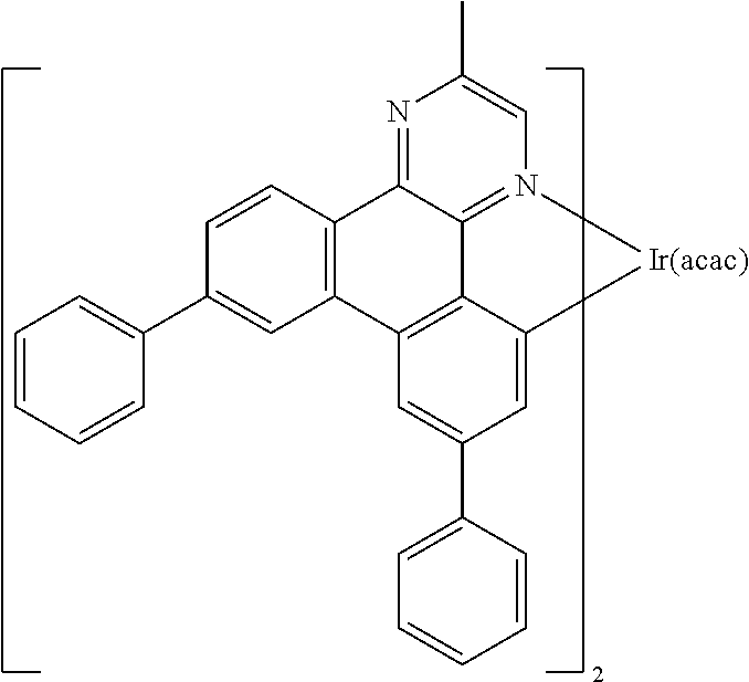 |
WO2009100991 | |
 |
WO2008101842 | |
| Platinum (II) organometallic complexes |
 |
WO2003040257 |
| Osminum (III) complexes |
 |
Chem. Mater. 17, 3532 (2005) |
| Ruthenium (II) complexes |
 |
Adv. Mater. 17, 1059 (2005) |
| Rhenium (I), (II), and (III) complexes |
 |
US20050244673 |
| Green dopants |
| Iridium (III) organometallic complexes |  |
Inorg. Chem. 40, 1704 (2001) |
 |
US20020034656 | |
 |
US7332232 | |
 |
US20090108737 | |
 |
US20090039776 | |
 |
US6921915 | |
 |
US6687266 | |
 |
Chem. Mater. 16, 2480 (2004) | |
 |
US20070190359 | |
 |
US 20060008670 JP2007123392 | |
 |
Adv. Mater. 16, 2003 (2004) | |
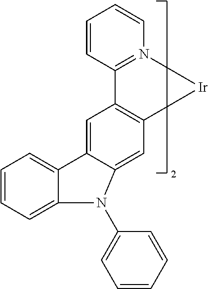 |
Angew. Chem. Int. Ed. 2006, 45, 7800 | |
 |
WO2009050290 | |
 |
US20090165846 | |
 |
US20080015355 | |
| Monomer for polymeric metal organometallic compounds |
 |
US7250226, US7396598 |
| Pt(II) organometallic complexes, including polydentated ligands |
 |
Appl. Phys. Lett. 86, 153505 (2005) |
 |
Appl. Phys. Lett. 86, 153505 (2005) | |
 |
Chem. Lett. 34, 592 (2005) | |
 |
WO2002015645 | |
 |
US20060263635 | |
| Cu complexes |
 |
WO2009000673 |
| Gold complexes |
 |
Chem. Commun. 2906 (2005) |
| Rhenium (III) complexes |
 |
Inorg. Chem. 42, 1248 (2003) |
| Deuterated organometallic complexes |
 |
US20030138657 |
| Organometallic complexes with two or more metal centers |
 |
US20030152802 |
 |
US7090928 | |
| Blue dopants |
| Iridium (III) organometallic complexes |
 |
WO2002002714 |
 |
WO2006009024 | |
 |
US20060251923 | |
 |
US7393599, WO2006056418, US20050260441, WO2005019373 | |
 |
US7534505 | |
 |
US7445855 | |
 |
US20070190359, US20080297033 | |
 |
US7338722 | |
 |
US20020134984 | |
 |
Angew. Chem. Int. Ed. 47, 1 (2008) | |
 |
Chem. Mater. 18, 5119 (2006) | |
 |
Inorg. Chem. 46, 4308 (2007) | |
 |
WO2005123873 | |
 |
WO2005123873 | |
 |
WO2007004380 | |
 |
WO2006082742 | |
| Osmium (II) complexes |
 |
US7279704 |
 |
Organometallics 23, 3745 (2004) | |
| Gold complexes |
|
Appl. Phys. Lett. 74, 1361 (1999) |
| Platinum (II) complexes |
 |
WO2006098120, WO2006103874 |
| Exciton/hole blocking layer materials |
| Bathocuprine compounds (e.g., BCP, BPhen) |
 |
Appl. Phys. Lett. 75, 4 (1999) |
 |
Appl. Phys. Lett. 79, 449 (2001) | |
| Metal 8- hydroxyquinolates (e.g., BAlq) |
 |
Appl. Phys. Lett 81, 162 (2002) |
| 5-member ring electron deficient heterocycles such as triazole, oxadiazole, imidazole, benzoimidazole |
 |
Appl. Phys. Lett 81, 162 (2002) |
| Triphenylene compounds |
 |
US20050025993 |
| Fluorinated aromatic compounds |
 |
Appl. Phys. Lett. 79, 156 (2001) |
| Phenothiazine- S-oxide |
 |
WO2008132085 |
| Electron transporting materials |
| Anthracene- benzoimidazole compounds |
 |
WO2003060956 |
 |
US20090179554 | |
| Aza triphenylene derivatives |
 |
US20090115316 |
| Anthracene- benzothiazole compounds |
 |
Appl. Phys. Lett. 89, 063504 (2006) |
| Metal 8- hydroxyquinolates (e.g., Alq3, Zrq4) |
 |
Appl. Phys. Lett. 51, 913 (1987) US7230107 |
| Metal hydroxy- benoquinolates |
 |
Chem. Lett. 5, 905 (1993) |
| Bathocuprine compounds such as BCP, BPhen, etc |
 |
Appl. Phys. Lett. 91, 263503 (2007) |
 |
Appl. Phys. Lett. 79, 449 (2001) | |
| 5-member ring electron deficient heterocycles (e.g.,triazole, oxadiazole, imidazole, benzoimidazole) |
 |
Appl. Phys. Lett. 74, 865 (1999) |
 |
Appl. Phys. Lett. 55, 1489 (1989) | |
 |
Jpn. J. Apply. Phys. 32, L917 (1993) | |
| Silole compounds |
 |
Org. Electron. 4, 113 (2003) |
| Arylborane compounds |
 |
J. Am. Chem. Soc. 120, 9714 (1998) |
| Fluorinated aromatic compounds |
 |
J. Am. Chem. Soc. 122, 1832 (2000) |
| Fullerene (e.g., C60) |
 |
US20090101870 |
| Triazine complexes |
 |
US20040036077 |
| Zn (N{circumflex over ( )}N) complexes |
 |
US6528187 |


Claims (17)
Y—X—Z, Formula I,


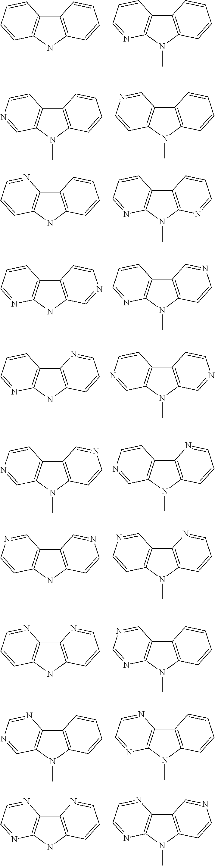


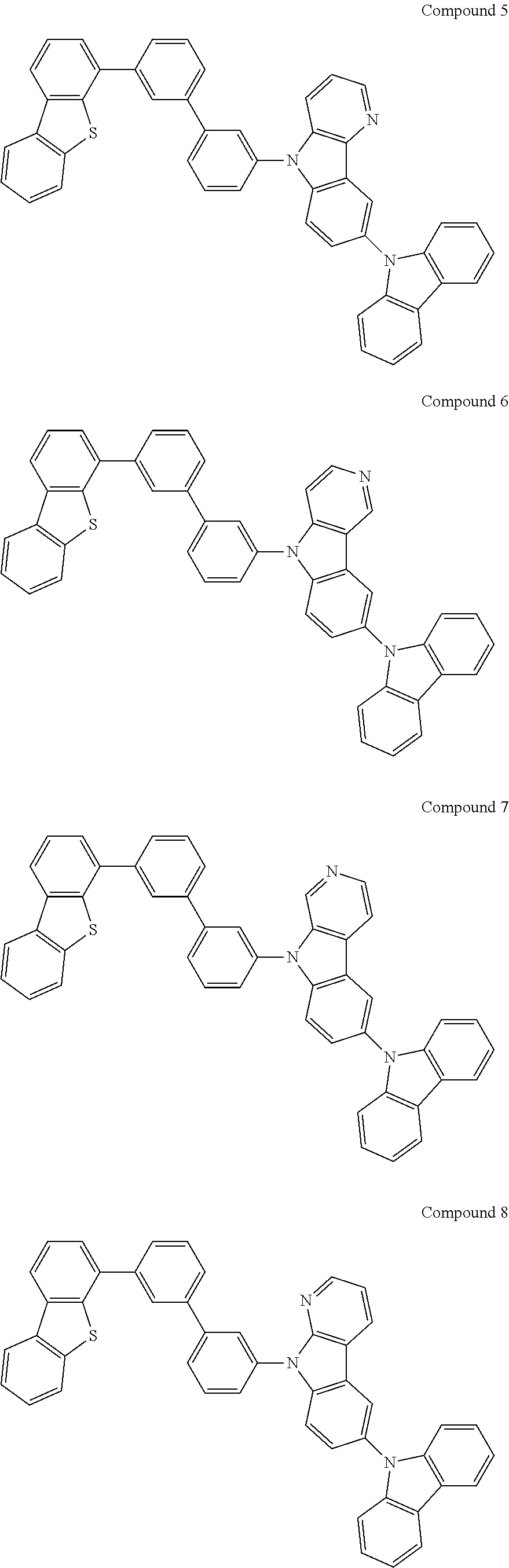


Y—X—Z Formula I,


Priority Applications (6)
| Application Number | Priority Date | Filing Date | Title |
|---|---|---|---|
| US13/082,914 US8580399B2 (en) | 2011-04-08 | 2011-04-08 | Substituted oligoazacarbazoles for light emitting diodes |
| PCT/US2012/032219 WO2012145173A1 (en) | 2011-04-08 | 2012-04-04 | Substituted oligoazacarbazoles for light emitting diodes |
| KR1020137029503A KR101950045B1 (en) | 2011-04-08 | 2012-04-04 | Substituted oligoazacarbazoles for light emitting diodes |
| EP12724783.1A EP2694503B1 (en) | 2011-04-08 | 2012-04-04 | Substituted oligoazacarbazoles for light emitting diodes |
| JP2014503965A JP5934337B2 (en) | 2011-04-08 | 2012-04-04 | Substituted oligoazacarbazoles for light-emitting diodes |
| TW101112365A TWI519625B (en) | 2011-04-08 | 2012-04-06 | Substituted oligoazacarbazoles for light emitting diodes |
Applications Claiming Priority (1)
| Application Number | Priority Date | Filing Date | Title |
|---|---|---|---|
| US13/082,914 US8580399B2 (en) | 2011-04-08 | 2011-04-08 | Substituted oligoazacarbazoles for light emitting diodes |
Publications (2)
| Publication Number | Publication Date |
|---|---|
| US20120256169A1 US20120256169A1 (en) | 2012-10-11 |
| US8580399B2 true US8580399B2 (en) | 2013-11-12 |
Family
ID=46197677
Family Applications (1)
| Application Number | Title | Priority Date | Filing Date |
|---|---|---|---|
| US13/082,914 Active 2031-08-07 US8580399B2 (en) | 2011-04-08 | 2011-04-08 | Substituted oligoazacarbazoles for light emitting diodes |
Country Status (6)
| Country | Link |
|---|---|
| US (1) | US8580399B2 (en) |
| EP (1) | EP2694503B1 (en) |
| JP (1) | JP5934337B2 (en) |
| KR (1) | KR101950045B1 (en) |
| TW (1) | TWI519625B (en) |
| WO (1) | WO2012145173A1 (en) |
Cited By (3)
| Publication number | Priority date | Publication date | Assignee | Title |
|---|---|---|---|---|
| US10600970B2 (en) | 2014-12-23 | 2020-03-24 | Merck Patent Gmbh | Carbazoles with two dibenzofuran or dibenzothiophene substituents |
| US11380851B2 (en) | 2017-09-01 | 2022-07-05 | Lg Chem, Ltd. | Compound and organic light emitting device comprising the same |
| US11737356B2 (en) | 2019-11-29 | 2023-08-22 | Samsung Display Co., Ltd. | Organic electroluminescence device and amine compound for organic electroluminescence device |
Families Citing this family (24)
| Publication number | Priority date | Publication date | Assignee | Title |
|---|---|---|---|---|
| WO2013077362A1 (en) | 2011-11-22 | 2013-05-30 | 出光興産株式会社 | Aromatic heterocyclic derivative, material for organic electroluminescent element, and organic electroluminescent element |
| JP5867137B2 (en) * | 2012-02-15 | 2016-02-24 | コニカミノルタ株式会社 | Organic electronics element, display device and lighting device |
| KR102044135B1 (en) * | 2012-11-28 | 2019-11-13 | 엘지디스플레이 주식회사 | Phosphorescent compound and Organic light emitting diode device using the same |
| JP6275378B2 (en) * | 2012-12-26 | 2018-02-07 | エヌ・イーケムキャット株式会社 | Process for producing carbazoles and carbazoles produced by this process. |
| US9302995B2 (en) | 2013-06-10 | 2016-04-05 | The United States Of America, As Represented By The Secretary Of The Navy | Electrically conducting oligo(pyrazoles) |
| CN109438518B (en) | 2013-07-02 | 2021-06-15 | Udc 爱尔兰有限责任公司 | Monosubstituted diazabenzimidazole carbene metal complexes for use in organic light emitting diodes |
| WO2015014835A1 (en) | 2013-07-31 | 2015-02-05 | Basf Se | Luminescent diazabenzimidazole carbene metal complexes |
| WO2015036080A1 (en) * | 2013-09-11 | 2015-03-19 | Merck Patent Gmbh | Organic electroluminescent device |
| US9458156B2 (en) | 2014-12-23 | 2016-10-04 | Bristol-Myers Squibb Company | Tricyclic compounds as anticancer agents |
| BR112016013744B1 (en) * | 2013-12-24 | 2022-08-30 | Bristol-Myers Squibb Company | TRICYCLIC COMPOUNDS AND THEIR USE AS ANTI-CANCER AGENTS |
| KR102330660B1 (en) | 2014-03-31 | 2021-11-24 | 유디씨 아일랜드 리미티드 | Metal complexes, comprising carbene ligands having an o-substituted non-cyclometalated aryl group and their use in organic light emitting diodes |
| EP3034507A1 (en) | 2014-12-15 | 2016-06-22 | Idemitsu Kosan Co., Ltd | 1-functionalized dibenzofurans and dibenzothiophenes for organic light emitting diodes (OLEDs) |
| JP6846876B2 (en) * | 2015-05-12 | 2021-03-24 | 株式会社半導体エネルギー研究所 | Compounds, light emitting elements, display modules, lighting modules, light emitting devices, display devices, lighting devices, and electronic devices |
| US9725449B2 (en) | 2015-05-12 | 2017-08-08 | Bristol-Myers Squibb Company | Tricyclic compounds as anticancer agents |
| JP2020113557A (en) * | 2017-03-28 | 2020-07-27 | 保土谷化学工業株式会社 | Compound having azacarbazole structure and organic electroluminescent device |
| JP6468314B2 (en) * | 2017-06-15 | 2019-02-13 | コニカミノルタ株式会社 | Organic electroluminescence element, lighting device and display device |
| CN109309163B (en) * | 2017-07-26 | 2019-12-17 | 清华大学 | Organic electroluminescent device |
| KR102450436B1 (en) | 2017-08-01 | 2022-10-04 | 삼성디스플레이 주식회사 | Heterocyclic compound and organic electroluminescence device including the same |
| CN108191853B (en) * | 2018-01-10 | 2020-08-07 | 北京鼎材科技有限公司 | Organic electroluminescent material and device |
| CN111683952B (en) * | 2018-06-07 | 2023-04-07 | 株式会社Lg化学 | Compound and organic light emitting device including the same |
| CN109678876A (en) * | 2018-11-08 | 2019-04-26 | 浙江华显光电科技有限公司 | A kind of red phosphorescent compound and its organic luminescent device using the compound |
| CN109678868A (en) * | 2018-11-08 | 2019-04-26 | 浙江华显光电科技有限公司 | A kind of red phosphorescent compound and its organic luminescent device using the compound |
| CN109503607A (en) * | 2018-11-26 | 2019-03-22 | 浙江华显光电科技有限公司 | A kind of phosphorescence host compound and its organic electroluminescence device using the compound |
| CN115232127B (en) * | 2022-08-04 | 2023-05-09 | 中钢集团南京新材料研究院有限公司 | Preparation method of alpha-carboline and alpha-carboline |
Citations (95)
| Publication number | Priority date | Publication date | Assignee | Title |
|---|---|---|---|---|
| US4769292A (en) | 1987-03-02 | 1988-09-06 | Eastman Kodak Company | Electroluminescent device with modified thin film luminescent zone |
| US5061589A (en) | 1988-06-24 | 1991-10-29 | Nippon Kayaku Kabushiki Kaisha | Toner for electrophotography |
| US5247190A (en) | 1989-04-20 | 1993-09-21 | Cambridge Research And Innovation Limited | Electroluminescent devices |
| EP0650955A1 (en) | 1993-11-01 | 1995-05-03 | Hodogaya Chemical Co., Ltd. | Amine compound and electro-luminescence device comprising same |
| US5703436A (en) | 1994-12-13 | 1997-12-30 | The Trustees Of Princeton University | Transparent contacts for organic devices |
| US5707745A (en) | 1994-12-13 | 1998-01-13 | The Trustees Of Princeton University | Multicolor organic light emitting devices |
| US5834893A (en) | 1996-12-23 | 1998-11-10 | The Trustees Of Princeton University | High efficiency organic light emitting devices with light directing structures |
| US5844363A (en) | 1997-01-23 | 1998-12-01 | The Trustees Of Princeton Univ. | Vacuum deposited, non-polymeric flexible organic light emitting devices |
| US6013982A (en) | 1996-12-23 | 2000-01-11 | The Trustees Of Princeton University | Multicolor display devices |
| US6087196A (en) | 1998-01-30 | 2000-07-11 | The Trustees Of Princeton University | Fabrication of organic semiconductor devices using ink jet printing |
| US6091195A (en) | 1997-02-03 | 2000-07-18 | The Trustees Of Princeton University | Displays having mesa pixel configuration |
| US6097147A (en) | 1998-09-14 | 2000-08-01 | The Trustees Of Princeton University | Structure for high efficiency electroluminescent device |
| WO2001039234A2 (en) | 1999-11-24 | 2001-05-31 | The Trustees Of Princeton University | Organic light emitting diode having a blue phosphorescent molecule as an emitter |
| US6294398B1 (en) | 1999-11-23 | 2001-09-25 | The Trustees Of Princeton University | Method for patterning devices |
| US6303238B1 (en) | 1997-12-01 | 2001-10-16 | The Trustees Of Princeton University | OLEDs doped with phosphorescent compounds |
| US6337102B1 (en) | 1997-11-17 | 2002-01-08 | The Trustees Of Princeton University | Low pressure vapor phase deposition of organic thin films |
| WO2002002714A2 (en) | 2000-06-30 | 2002-01-10 | E.I. Du Pont De Nemours And Company | Electroluminescent iridium compounds with fluorinated phenylpyridines, phenylpyrimidines, and phenylquinolines and devices made with such compounds |
| WO2002015645A1 (en) | 2000-08-11 | 2002-02-21 | The Trustees Of Princeton University | Organometallic compounds and emission-shifting organic electrophosphorescence |
| US20020034856A1 (en) | 2000-06-29 | 2002-03-21 | Jeon Kwang-Seok | Method for forming junction electrode of semiconductor device |
| US20020134984A1 (en) | 2001-02-01 | 2002-09-26 | Fuji Photo Film Co., Ltd. | Transition metal complex and light-emitting device |
| US20020158242A1 (en) | 1999-12-31 | 2002-10-31 | Se-Hwan Son | Electronic device comprising organic compound having p-type semiconducting characteristics |
| US6528187B1 (en) | 1998-09-08 | 2003-03-04 | Fuji Photo Film Co., Ltd. | Material for luminescence element and luminescence element using the same |
| WO2003040257A1 (en) | 2001-11-07 | 2003-05-15 | E. I. Du Pont De Nemours And Company | Electroluminescent platinum compounds and devices made with such compounds |
| WO2003060956A2 (en) | 2002-01-18 | 2003-07-24 | Lg Chem, Ltd. | New material for transporting electrons and organic electroluminescent display using the same |
| US20030138657A1 (en) | 2000-12-07 | 2003-07-24 | Canon Kabushiki Kaisha | Deuterated semi-conducting organic compounds used for opto-electronic devices |
| US20030152802A1 (en) | 2001-06-19 | 2003-08-14 | Akira Tsuboyama | Metal coordination compound and organic liminescence device |
| US20030162053A1 (en) | 1996-06-25 | 2003-08-28 | Marks Tobin J. | Organic light - emitting diodes and methods for assembly and enhanced charge injection |
| US20030175553A1 (en) | 2001-12-28 | 2003-09-18 | Thompson Mark E. | White light emitting oleds from combined monomer and aggregate emission |
| US20030230980A1 (en) | 2002-06-18 | 2003-12-18 | Forrest Stephen R | Very low voltage, high efficiency phosphorescent oled in a p-i-n structure |
| US6687266B1 (en) | 2002-11-08 | 2004-02-03 | Universal Display Corporation | Organic light emitting materials and devices |
| US20040036077A1 (en) | 2002-08-22 | 2004-02-26 | Fuji Photo Film Co., Ltd. | Light emitting element |
| US20040137267A1 (en) | 2002-12-27 | 2004-07-15 | Fuji Photo Film Co., Ltd. | Organic electroluminescent device |
| US20040137268A1 (en) | 2002-12-27 | 2004-07-15 | Fuji Photo Film Co., Ltd. | Organic electroluminescent device |
| US20040174116A1 (en) | 2001-08-20 | 2004-09-09 | Lu Min-Hao Michael | Transparent electrodes |
| WO2004093207A2 (en) | 2003-04-15 | 2004-10-28 | Covion Organic Semiconductors Gmbh | Mixtures of matrix materials and organic semiconductors capable of emission, use of the same and electronic components containing said mixtures |
| WO2004107822A1 (en) | 2003-05-29 | 2004-12-09 | Nippon Steel Chemical Co., Ltd. | Organic electroluminescent element |
| US6835469B2 (en) | 2001-10-17 | 2004-12-28 | The University Of Southern California | Phosphorescent compounds and devices comprising the same |
| JP2005011610A (en) | 2003-06-18 | 2005-01-13 | Nippon Steel Chem Co Ltd | Organic electroluminescent element |
| US20050025993A1 (en) | 2003-07-25 | 2005-02-03 | Thompson Mark E. | Materials and structures for enhancing the performance of organic light emitting devices |
| WO2005014551A1 (en) | 2003-08-07 | 2005-02-17 | Nippon Steel Chemical Co., Ltd. | Aluminum chelate compelx for organic el material |
| US20050112407A1 (en) | 2003-11-21 | 2005-05-26 | Fuji Photo Film Co., Ltd. | Organic electroluminescent device |
| US6921915B2 (en) | 2001-03-08 | 2005-07-26 | Canon Kabushiki Kaisha | Metal coordination compound, luminescence device and display apparatus |
| US20050238919A1 (en) | 2004-04-23 | 2005-10-27 | Fuji Photo Film Co., Ltd. | Organic electroluminescent device |
| US20050244673A1 (en) | 2002-08-27 | 2005-11-03 | Fujitsu Limited | Organometallic complex, organic EL element and organic EL display |
| US20050260441A1 (en) | 2004-05-18 | 2005-11-24 | Thompson Mark E | Luminescent compounds with carbene ligands |
| US20050260449A1 (en) | 2004-05-18 | 2005-11-24 | Robert Walters | Complexes with tridentate ligands |
| US20060008670A1 (en) | 2004-07-06 | 2006-01-12 | Chun Lin | Organic light emitting materials and devices |
| US7087321B2 (en) | 2003-04-22 | 2006-08-08 | Universal Display Corporation | Organic light emitting devices having reduced pixel shrinkage |
| US7090928B2 (en) | 2003-04-01 | 2006-08-15 | The University Of Southern California | Binuclear compounds |
| US20060202194A1 (en) | 2005-03-08 | 2006-09-14 | Jeong Hyun C | Red phosphorescene compounds and organic electroluminescence device using the same |
| US20060240279A1 (en) | 2005-04-21 | 2006-10-26 | Vadim Adamovich | Non-blocked phosphorescent OLEDs |
| US20060251923A1 (en) | 2005-05-06 | 2006-11-09 | Chun Lin | Stability OLED materials and devices |
| EP1725079A1 (en) | 2004-03-11 | 2006-11-22 | Mitsubishi Chemical Corporation | Composition for charge-transporting film and ion compound, charge-transporting film and organic electroluminescent device using same, and method for manufacturing organic electroluminescent device and method for producing charge-transporting film |
| US20060263635A1 (en) | 2005-05-06 | 2006-11-23 | Fuji Photo Film Co., Ltd. | Organic electroluminescent device |
| US20060280965A1 (en) | 2005-05-31 | 2006-12-14 | Raymond Kwong | Triphenylene hosts in phosphorescent light emitting diodes |
| US7154114B2 (en) | 2004-05-18 | 2006-12-26 | Universal Display Corporation | Cyclometallated iridium carbene complexes for use as hosts |
| JP2007123392A (en) | 2005-10-26 | 2007-05-17 | Konica Minolta Holdings Inc | Organic electroluminescence device, display device and lighting device |
| US7250226B2 (en) | 2001-08-31 | 2007-07-31 | Nippon Hoso Kyokai | Phosphorescent compound, a phosphorescent composition and an organic light-emitting device |
| US20070190359A1 (en) | 2006-02-10 | 2007-08-16 | Knowles David B | Metal complexes of cyclometallated imidazo[1,2-ƒ]phenanthridine and diimidazo[1,2-a:1',2'-c]quinazoline ligands and isoelectronic and benzannulated analogs thereof |
| JP2007254297A (en) | 2006-03-20 | 2007-10-04 | Nippon Steel Chem Co Ltd | Compound of light-emitting layer and organic electroluminescent device |
| US20070278938A1 (en) | 2006-04-26 | 2007-12-06 | Idemitsu Kosan Co., Ltd. | Aromatic amine derivative and electroluminescence device using the same |
| US20080015355A1 (en) | 2004-06-28 | 2008-01-17 | Thomas Schafer | Electroluminescent Metal Complexes With Triazoles And Benzotriazoles |
| US20080018221A1 (en) | 2004-11-25 | 2008-01-24 | Basf Aktiengesellschaft | Use Of Transition Metal Carbene Complexes In Organic Light-Emitting Diodes (Oleds) |
| US7332232B2 (en) | 2004-02-03 | 2008-02-19 | Universal Display Corporation | OLEDs utilizing multidentate ligand systems |
| US7338722B2 (en) | 2003-03-24 | 2008-03-04 | The University Of Southern California | Phenyl and fluorenyl substituted phenyl-pyrazole complexes of Ir |
| JP2008074939A (en) | 2006-09-21 | 2008-04-03 | Konica Minolta Holdings Inc | Organic electroluminescence element material, organic electroluminescence element, display device and illumination device |
| US20080106190A1 (en) | 2006-08-23 | 2008-05-08 | Idemitsu Kosan Co., Ltd. | Aromatic amine derivatives and organic electroluminescent device using same |
| US20080124572A1 (en) | 2006-11-24 | 2008-05-29 | Idemitsu Kosan Co., Ltd. | Aromatic amine derivative and organic electroluminescence device using the same |
| US7393599B2 (en) | 2004-05-18 | 2008-07-01 | The University Of Southern California | Luminescent compounds with carbene ligands |
| US7396598B2 (en) | 2001-06-20 | 2008-07-08 | Showa Denko K.K. | Light emitting material and organic light-emitting device |
| US20080220265A1 (en) | 2006-12-08 | 2008-09-11 | Universal Display Corporation | Cross-linkable Iridium Complexes and Organic Light-Emitting Devices Using the Same |
| US7431968B1 (en) | 2001-09-04 | 2008-10-07 | The Trustees Of Princeton University | Process and apparatus for organic vapor jet deposition |
| US7445855B2 (en) | 2004-05-18 | 2008-11-04 | The University Of Southern California | Cationic metal-carbene complexes |
| US20080297033A1 (en) | 2006-02-10 | 2008-12-04 | Knowles David B | Blue phosphorescent imidazophenanthridine materials |
| US20090009065A1 (en) | 2007-07-07 | 2009-01-08 | Idemitsu Kosan Co., Ltd. | Organic electroluminescence device and material for organic electroluminescence device |
| US20090008605A1 (en) | 2007-07-07 | 2009-01-08 | Idemitsu Kosan Co., Ltd. | Naphthalene derivative, material for organic electroluminescence device, and organic electroluminescence device using the same |
| US20090017330A1 (en) | 2007-07-10 | 2009-01-15 | Idemitsu Kosan Co., Ltd. | Material for organic electroluminescence device and organic electroluminescence device utilizing the same |
| US20090030202A1 (en) | 2007-07-10 | 2009-01-29 | Idemitsu Kosan Co., Ltd. | Material for organic electroluminescent element and organic electroluminescent element employing the same |
| US20090039776A1 (en) | 2007-08-09 | 2009-02-12 | Canon Kabushiki Kaisha | Organometallic complex and organic light-emitting element using same |
| US20090045731A1 (en) | 2007-07-07 | 2009-02-19 | Idemitsu Kosan Co., Ltd. | Organic electroluminescence device and material for organic electroluminescence device |
| US20090045730A1 (en) | 2007-07-07 | 2009-02-19 | Idemitsu Kosan Co., Ltd. | Organic electroluminescence device and material for organic electroluminescence device |
| EP2034538A1 (en) | 2006-06-02 | 2009-03-11 | Idemitsu Kosan Co., Ltd. | Material for organic electroluminescence element, and organic electroluminescence element using the material |
| US20090101870A1 (en) | 2007-10-22 | 2009-04-23 | E. I. Du Pont De Nemours And Company | Electron transport bi-layers and devices made with such bi-layers |
| US20090108737A1 (en) | 2006-12-08 | 2009-04-30 | Raymond Kwong | Light-emitting organometallic complexes |
| US20090115316A1 (en) | 2007-11-02 | 2009-05-07 | Shiying Zheng | Organic electroluminescent device having an azatriphenylene derivative |
| US7534505B2 (en) | 2004-05-18 | 2009-05-19 | The University Of Southern California | Organometallic compounds for use in electroluminescent devices |
| US20090167162A1 (en) | 2007-12-28 | 2009-07-02 | Universal Display Corporation | Dibenzothiophene-containing materials in phosphorescent light emitting diodes |
| US20090165846A1 (en) | 2005-09-07 | 2009-07-02 | Universitaet Braunschweig | Triplet emitter having condensed five-membered rings |
| US20090179554A1 (en) | 2006-05-11 | 2009-07-16 | Hitoshi Kuma | Organic electroluminescent device |
| EP2123733A2 (en) | 2008-05-13 | 2009-11-25 | Konica Minolta Holdings, Inc. | Organic electroluminescent element, display device and lighting device |
| US20100141127A1 (en) | 2008-11-11 | 2010-06-10 | Universal Display Corporation | Phosphorescent emitters |
| JP2010135467A (en) | 2008-12-03 | 2010-06-17 | Konica Minolta Holdings Inc | Organic electroluminescent element, lighting system equipped with the element, and display device |
| WO2010090077A1 (en) | 2009-02-06 | 2010-08-12 | コニカミノルタホールディングス株式会社 | Organic electroluminescent element, and illumination device and display device each comprising the element |
| US20100244004A1 (en) | 2009-03-23 | 2010-09-30 | Universal Display Corporation | Heteroleptic iridium complex |
| JP2011008991A (en) | 2009-06-24 | 2011-01-13 | Konica Minolta Holdings Inc | Organic electroluminescent element, white organic electroluminescent element, display device and illumination device |
Family Cites Families (10)
| Publication number | Priority date | Publication date | Assignee | Title |
|---|---|---|---|---|
| US7935434B2 (en) * | 2006-01-05 | 2011-05-03 | Konica Minolta Holdings, Inc. | Organic electroluminescent device, display, and illuminating device |
| WO2009060757A1 (en) * | 2007-11-08 | 2009-05-14 | Konica Minolta Holdings, Inc. | Organic electroluminescent device, display device and illuminating device |
| US8221905B2 (en) | 2007-12-28 | 2012-07-17 | Universal Display Corporation | Carbazole-containing materials in phosphorescent light emitting diodes |
| WO2010044342A1 (en) * | 2008-10-15 | 2010-04-22 | コニカミノルタホールディングス株式会社 | Organic el element, organic el element manufacturing method, white organic el element, display device, and illumination device |
| US9067947B2 (en) * | 2009-01-16 | 2015-06-30 | Universal Display Corporation | Organic electroluminescent materials and devices |
| JP5472301B2 (en) * | 2009-07-07 | 2014-04-16 | コニカミノルタ株式会社 | ORGANIC ELECTROLUMINESCENT ELEMENT, NOVEL COMPOUND, LIGHTING DEVICE AND DISPLAY DEVICE |
| JP5604848B2 (en) * | 2009-10-19 | 2014-10-15 | コニカミノルタ株式会社 | ORGANIC ELECTROLUMINESCENT ELEMENT MATERIAL, ORGANIC ELECTROLUMINESCENT ELEMENT, LIGHTING DEVICE AND DISPLAY DEVICE |
| KR101419666B1 (en) * | 2010-03-31 | 2014-07-15 | 이데미쓰 고산 가부시키가이샤 | Material for organic electroluminescence element, and organic electroluminescence element using same |
| JP6007467B2 (en) * | 2010-07-27 | 2016-10-12 | コニカミノルタ株式会社 | Organic electroluminescence element material, organic electroluminescence element, |
| US8932734B2 (en) * | 2010-10-08 | 2015-01-13 | Universal Display Corporation | Organic electroluminescent materials and devices |
-
2011
- 2011-04-08 US US13/082,914 patent/US8580399B2/en active Active
-
2012
- 2012-04-04 WO PCT/US2012/032219 patent/WO2012145173A1/en active Application Filing
- 2012-04-04 JP JP2014503965A patent/JP5934337B2/en active Active
- 2012-04-04 EP EP12724783.1A patent/EP2694503B1/en active Active
- 2012-04-04 KR KR1020137029503A patent/KR101950045B1/en active IP Right Grant
- 2012-04-06 TW TW101112365A patent/TWI519625B/en active
Patent Citations (100)
| Publication number | Priority date | Publication date | Assignee | Title |
|---|---|---|---|---|
| US4769292A (en) | 1987-03-02 | 1988-09-06 | Eastman Kodak Company | Electroluminescent device with modified thin film luminescent zone |
| US5061589A (en) | 1988-06-24 | 1991-10-29 | Nippon Kayaku Kabushiki Kaisha | Toner for electrophotography |
| US5247190A (en) | 1989-04-20 | 1993-09-21 | Cambridge Research And Innovation Limited | Electroluminescent devices |
| EP0650955A1 (en) | 1993-11-01 | 1995-05-03 | Hodogaya Chemical Co., Ltd. | Amine compound and electro-luminescence device comprising same |
| US5703436A (en) | 1994-12-13 | 1997-12-30 | The Trustees Of Princeton University | Transparent contacts for organic devices |
| US5707745A (en) | 1994-12-13 | 1998-01-13 | The Trustees Of Princeton University | Multicolor organic light emitting devices |
| US20030162053A1 (en) | 1996-06-25 | 2003-08-28 | Marks Tobin J. | Organic light - emitting diodes and methods for assembly and enhanced charge injection |
| US5834893A (en) | 1996-12-23 | 1998-11-10 | The Trustees Of Princeton University | High efficiency organic light emitting devices with light directing structures |
| US6013982A (en) | 1996-12-23 | 2000-01-11 | The Trustees Of Princeton University | Multicolor display devices |
| US5844363A (en) | 1997-01-23 | 1998-12-01 | The Trustees Of Princeton Univ. | Vacuum deposited, non-polymeric flexible organic light emitting devices |
| US6091195A (en) | 1997-02-03 | 2000-07-18 | The Trustees Of Princeton University | Displays having mesa pixel configuration |
| US6337102B1 (en) | 1997-11-17 | 2002-01-08 | The Trustees Of Princeton University | Low pressure vapor phase deposition of organic thin films |
| US6303238B1 (en) | 1997-12-01 | 2001-10-16 | The Trustees Of Princeton University | OLEDs doped with phosphorescent compounds |
| US6087196A (en) | 1998-01-30 | 2000-07-11 | The Trustees Of Princeton University | Fabrication of organic semiconductor devices using ink jet printing |
| US6528187B1 (en) | 1998-09-08 | 2003-03-04 | Fuji Photo Film Co., Ltd. | Material for luminescence element and luminescence element using the same |
| US6097147A (en) | 1998-09-14 | 2000-08-01 | The Trustees Of Princeton University | Structure for high efficiency electroluminescent device |
| US6294398B1 (en) | 1999-11-23 | 2001-09-25 | The Trustees Of Princeton University | Method for patterning devices |
| US6468819B1 (en) | 1999-11-23 | 2002-10-22 | The Trustees Of Princeton University | Method for patterning organic thin film devices using a die |
| WO2001039234A2 (en) | 1999-11-24 | 2001-05-31 | The Trustees Of Princeton University | Organic light emitting diode having a blue phosphorescent molecule as an emitter |
| US20020158242A1 (en) | 1999-12-31 | 2002-10-31 | Se-Hwan Son | Electronic device comprising organic compound having p-type semiconducting characteristics |
| US20020034856A1 (en) | 2000-06-29 | 2002-03-21 | Jeon Kwang-Seok | Method for forming junction electrode of semiconductor device |
| WO2002002714A2 (en) | 2000-06-30 | 2002-01-10 | E.I. Du Pont De Nemours And Company | Electroluminescent iridium compounds with fluorinated phenylpyridines, phenylpyrimidines, and phenylquinolines and devices made with such compounds |
| WO2002015645A1 (en) | 2000-08-11 | 2002-02-21 | The Trustees Of Princeton University | Organometallic compounds and emission-shifting organic electrophosphorescence |
| US20030138657A1 (en) | 2000-12-07 | 2003-07-24 | Canon Kabushiki Kaisha | Deuterated semi-conducting organic compounds used for opto-electronic devices |
| US20020134984A1 (en) | 2001-02-01 | 2002-09-26 | Fuji Photo Film Co., Ltd. | Transition metal complex and light-emitting device |
| US6921915B2 (en) | 2001-03-08 | 2005-07-26 | Canon Kabushiki Kaisha | Metal coordination compound, luminescence device and display apparatus |
| US20030152802A1 (en) | 2001-06-19 | 2003-08-14 | Akira Tsuboyama | Metal coordination compound and organic liminescence device |
| US7396598B2 (en) | 2001-06-20 | 2008-07-08 | Showa Denko K.K. | Light emitting material and organic light-emitting device |
| US20040174116A1 (en) | 2001-08-20 | 2004-09-09 | Lu Min-Hao Michael | Transparent electrodes |
| US7250226B2 (en) | 2001-08-31 | 2007-07-31 | Nippon Hoso Kyokai | Phosphorescent compound, a phosphorescent composition and an organic light-emitting device |
| US7431968B1 (en) | 2001-09-04 | 2008-10-07 | The Trustees Of Princeton University | Process and apparatus for organic vapor jet deposition |
| US6835469B2 (en) | 2001-10-17 | 2004-12-28 | The University Of Southern California | Phosphorescent compounds and devices comprising the same |
| WO2003040257A1 (en) | 2001-11-07 | 2003-05-15 | E. I. Du Pont De Nemours And Company | Electroluminescent platinum compounds and devices made with such compounds |
| US20030175553A1 (en) | 2001-12-28 | 2003-09-18 | Thompson Mark E. | White light emitting oleds from combined monomer and aggregate emission |
| WO2003060956A2 (en) | 2002-01-18 | 2003-07-24 | Lg Chem, Ltd. | New material for transporting electrons and organic electroluminescent display using the same |
| US20030230980A1 (en) | 2002-06-18 | 2003-12-18 | Forrest Stephen R | Very low voltage, high efficiency phosphorescent oled in a p-i-n structure |
| US20040036077A1 (en) | 2002-08-22 | 2004-02-26 | Fuji Photo Film Co., Ltd. | Light emitting element |
| US20050244673A1 (en) | 2002-08-27 | 2005-11-03 | Fujitsu Limited | Organometallic complex, organic EL element and organic EL display |
| US6687266B1 (en) | 2002-11-08 | 2004-02-03 | Universal Display Corporation | Organic light emitting materials and devices |
| US20040137267A1 (en) | 2002-12-27 | 2004-07-15 | Fuji Photo Film Co., Ltd. | Organic electroluminescent device |
| US20040137268A1 (en) | 2002-12-27 | 2004-07-15 | Fuji Photo Film Co., Ltd. | Organic electroluminescent device |
| US7338722B2 (en) | 2003-03-24 | 2008-03-04 | The University Of Southern California | Phenyl and fluorenyl substituted phenyl-pyrazole complexes of Ir |
| US7090928B2 (en) | 2003-04-01 | 2006-08-15 | The University Of Southern California | Binuclear compounds |
| WO2004093207A2 (en) | 2003-04-15 | 2004-10-28 | Covion Organic Semiconductors Gmbh | Mixtures of matrix materials and organic semiconductors capable of emission, use of the same and electronic components containing said mixtures |
| US7087321B2 (en) | 2003-04-22 | 2006-08-08 | Universal Display Corporation | Organic light emitting devices having reduced pixel shrinkage |
| WO2004107822A1 (en) | 2003-05-29 | 2004-12-09 | Nippon Steel Chemical Co., Ltd. | Organic electroluminescent element |
| JP2005011610A (en) | 2003-06-18 | 2005-01-13 | Nippon Steel Chem Co Ltd | Organic electroluminescent element |
| US20050025993A1 (en) | 2003-07-25 | 2005-02-03 | Thompson Mark E. | Materials and structures for enhancing the performance of organic light emitting devices |
| WO2005014551A1 (en) | 2003-08-07 | 2005-02-17 | Nippon Steel Chemical Co., Ltd. | Aluminum chelate compelx for organic el material |
| US20050112407A1 (en) | 2003-11-21 | 2005-05-26 | Fuji Photo Film Co., Ltd. | Organic electroluminescent device |
| US7332232B2 (en) | 2004-02-03 | 2008-02-19 | Universal Display Corporation | OLEDs utilizing multidentate ligand systems |
| EP1725079A1 (en) | 2004-03-11 | 2006-11-22 | Mitsubishi Chemical Corporation | Composition for charge-transporting film and ion compound, charge-transporting film and organic electroluminescent device using same, and method for manufacturing organic electroluminescent device and method for producing charge-transporting film |
| US20050238919A1 (en) | 2004-04-23 | 2005-10-27 | Fuji Photo Film Co., Ltd. | Organic electroluminescent device |
| US7445855B2 (en) | 2004-05-18 | 2008-11-04 | The University Of Southern California | Cationic metal-carbene complexes |
| US7534505B2 (en) | 2004-05-18 | 2009-05-19 | The University Of Southern California | Organometallic compounds for use in electroluminescent devices |
| US7154114B2 (en) | 2004-05-18 | 2006-12-26 | Universal Display Corporation | Cyclometallated iridium carbene complexes for use as hosts |
| US7393599B2 (en) | 2004-05-18 | 2008-07-01 | The University Of Southern California | Luminescent compounds with carbene ligands |
| US20050260449A1 (en) | 2004-05-18 | 2005-11-24 | Robert Walters | Complexes with tridentate ligands |
| US20050260441A1 (en) | 2004-05-18 | 2005-11-24 | Thompson Mark E | Luminescent compounds with carbene ligands |
| US7279704B2 (en) | 2004-05-18 | 2007-10-09 | The University Of Southern California | Complexes with tridentate ligands |
| US20080015355A1 (en) | 2004-06-28 | 2008-01-17 | Thomas Schafer | Electroluminescent Metal Complexes With Triazoles And Benzotriazoles |
| US20060008670A1 (en) | 2004-07-06 | 2006-01-12 | Chun Lin | Organic light emitting materials and devices |
| US20080018221A1 (en) | 2004-11-25 | 2008-01-24 | Basf Aktiengesellschaft | Use Of Transition Metal Carbene Complexes In Organic Light-Emitting Diodes (Oleds) |
| US20060202194A1 (en) | 2005-03-08 | 2006-09-14 | Jeong Hyun C | Red phosphorescene compounds and organic electroluminescence device using the same |
| US20060240279A1 (en) | 2005-04-21 | 2006-10-26 | Vadim Adamovich | Non-blocked phosphorescent OLEDs |
| US20060251923A1 (en) | 2005-05-06 | 2006-11-09 | Chun Lin | Stability OLED materials and devices |
| US20060263635A1 (en) | 2005-05-06 | 2006-11-23 | Fuji Photo Film Co., Ltd. | Organic electroluminescent device |
| US20060280965A1 (en) | 2005-05-31 | 2006-12-14 | Raymond Kwong | Triphenylene hosts in phosphorescent light emitting diodes |
| US20090165846A1 (en) | 2005-09-07 | 2009-07-02 | Universitaet Braunschweig | Triplet emitter having condensed five-membered rings |
| JP2007123392A (en) | 2005-10-26 | 2007-05-17 | Konica Minolta Holdings Inc | Organic electroluminescence device, display device and lighting device |
| US20070190359A1 (en) | 2006-02-10 | 2007-08-16 | Knowles David B | Metal complexes of cyclometallated imidazo[1,2-ƒ]phenanthridine and diimidazo[1,2-a:1',2'-c]quinazoline ligands and isoelectronic and benzannulated analogs thereof |
| US20080297033A1 (en) | 2006-02-10 | 2008-12-04 | Knowles David B | Blue phosphorescent imidazophenanthridine materials |
| JP2007254297A (en) | 2006-03-20 | 2007-10-04 | Nippon Steel Chem Co Ltd | Compound of light-emitting layer and organic electroluminescent device |
| US20070278938A1 (en) | 2006-04-26 | 2007-12-06 | Idemitsu Kosan Co., Ltd. | Aromatic amine derivative and electroluminescence device using the same |
| US20090179554A1 (en) | 2006-05-11 | 2009-07-16 | Hitoshi Kuma | Organic electroluminescent device |
| EP2034538A1 (en) | 2006-06-02 | 2009-03-11 | Idemitsu Kosan Co., Ltd. | Material for organic electroluminescence element, and organic electroluminescence element using the material |
| US20080106190A1 (en) | 2006-08-23 | 2008-05-08 | Idemitsu Kosan Co., Ltd. | Aromatic amine derivatives and organic electroluminescent device using same |
| JP2008074939A (en) | 2006-09-21 | 2008-04-03 | Konica Minolta Holdings Inc | Organic electroluminescence element material, organic electroluminescence element, display device and illumination device |
| US20080124572A1 (en) | 2006-11-24 | 2008-05-29 | Idemitsu Kosan Co., Ltd. | Aromatic amine derivative and organic electroluminescence device using the same |
| US20080220265A1 (en) | 2006-12-08 | 2008-09-11 | Universal Display Corporation | Cross-linkable Iridium Complexes and Organic Light-Emitting Devices Using the Same |
| US20090108737A1 (en) | 2006-12-08 | 2009-04-30 | Raymond Kwong | Light-emitting organometallic complexes |
| US20090045731A1 (en) | 2007-07-07 | 2009-02-19 | Idemitsu Kosan Co., Ltd. | Organic electroluminescence device and material for organic electroluminescence device |
| US20090009065A1 (en) | 2007-07-07 | 2009-01-08 | Idemitsu Kosan Co., Ltd. | Organic electroluminescence device and material for organic electroluminescence device |
| US20090008605A1 (en) | 2007-07-07 | 2009-01-08 | Idemitsu Kosan Co., Ltd. | Naphthalene derivative, material for organic electroluminescence device, and organic electroluminescence device using the same |
| US20090045730A1 (en) | 2007-07-07 | 2009-02-19 | Idemitsu Kosan Co., Ltd. | Organic electroluminescence device and material for organic electroluminescence device |
| US20090030202A1 (en) | 2007-07-10 | 2009-01-29 | Idemitsu Kosan Co., Ltd. | Material for organic electroluminescent element and organic electroluminescent element employing the same |
| US20090017330A1 (en) | 2007-07-10 | 2009-01-15 | Idemitsu Kosan Co., Ltd. | Material for organic electroluminescence device and organic electroluminescence device utilizing the same |
| EP2166583A1 (en) | 2007-07-10 | 2010-03-24 | Idemitsu Kosan Co., Ltd. | Material for organic electroluminescence element, and organic electroluminescence element prepared by using the material |
| US20090039776A1 (en) | 2007-08-09 | 2009-02-12 | Canon Kabushiki Kaisha | Organometallic complex and organic light-emitting element using same |
| US20090101870A1 (en) | 2007-10-22 | 2009-04-23 | E. I. Du Pont De Nemours And Company | Electron transport bi-layers and devices made with such bi-layers |
| US20090115316A1 (en) | 2007-11-02 | 2009-05-07 | Shiying Zheng | Organic electroluminescent device having an azatriphenylene derivative |
| WO2009085344A2 (en) | 2007-12-28 | 2009-07-09 | Universal Display Corporation | Dibenzothiophene-containing materials in phosphorescent light emitting diodes |
| US20090167162A1 (en) | 2007-12-28 | 2009-07-02 | Universal Display Corporation | Dibenzothiophene-containing materials in phosphorescent light emitting diodes |
| EP2123733A2 (en) | 2008-05-13 | 2009-11-25 | Konica Minolta Holdings, Inc. | Organic electroluminescent element, display device and lighting device |
| US20100141127A1 (en) | 2008-11-11 | 2010-06-10 | Universal Display Corporation | Phosphorescent emitters |
| JP2010135467A (en) | 2008-12-03 | 2010-06-17 | Konica Minolta Holdings Inc | Organic electroluminescent element, lighting system equipped with the element, and display device |
| WO2010090077A1 (en) | 2009-02-06 | 2010-08-12 | コニカミノルタホールディングス株式会社 | Organic electroluminescent element, and illumination device and display device each comprising the element |
| EP2395573A1 (en) | 2009-02-06 | 2011-12-14 | Konica Minolta Holdings, Inc. | Organic electroluminescent element, and illumination device and display device each comprising the element |
| US20100244004A1 (en) | 2009-03-23 | 2010-09-30 | Universal Display Corporation | Heteroleptic iridium complex |
| JP2011008991A (en) | 2009-06-24 | 2011-01-13 | Konica Minolta Holdings Inc | Organic electroluminescent element, white organic electroluminescent element, display device and illumination device |
Non-Patent Citations (52)
Cited By (3)
| Publication number | Priority date | Publication date | Assignee | Title |
|---|---|---|---|---|
| US10600970B2 (en) | 2014-12-23 | 2020-03-24 | Merck Patent Gmbh | Carbazoles with two dibenzofuran or dibenzothiophene substituents |
| US11380851B2 (en) | 2017-09-01 | 2022-07-05 | Lg Chem, Ltd. | Compound and organic light emitting device comprising the same |
| US11737356B2 (en) | 2019-11-29 | 2023-08-22 | Samsung Display Co., Ltd. | Organic electroluminescence device and amine compound for organic electroluminescence device |
Also Published As
| Publication number | Publication date |
|---|---|
| TWI519625B (en) | 2016-02-01 |
| WO2012145173A1 (en) | 2012-10-26 |
| US20120256169A1 (en) | 2012-10-11 |
| KR101950045B1 (en) | 2019-02-19 |
| JP2014511861A (en) | 2014-05-19 |
| EP2694503B1 (en) | 2017-03-08 |
| TW201245409A (en) | 2012-11-16 |
| KR20140025445A (en) | 2014-03-04 |
| JP5934337B2 (en) | 2016-06-15 |
| EP2694503A1 (en) | 2014-02-12 |
Similar Documents
| Publication | Publication Date | Title |
|---|---|---|
| US20220216421A1 (en) | Organic electroluminescent materials and devices | |
| US8580399B2 (en) | Substituted oligoazacarbazoles for light emitting diodes | |
| US8748012B2 (en) | Host materials for OLED | |
| US9548459B2 (en) | Organic materials for organic light emitting devices | |
| US9461254B2 (en) | Organic electroluminescent materials and devices | |
| US9673401B2 (en) | Organic electroluminescent materials and devices | |
| US10211413B2 (en) | Organic electroluminescent materials and devices | |
| US10461260B2 (en) | Organic electroluminescent materials and devices | |
| US8409729B2 (en) | Host materials for phosphorescent OLEDs | |
| US8415031B2 (en) | Electron transporting compounds | |
| US9142788B2 (en) | Host materials for OLEDs | |
| US9193745B2 (en) | Heteroleptic iridium complex | |
| US9175211B2 (en) | Phosphorescent materials | |
| US9184399B2 (en) | Asymmetric hosts with triaryl silane side chains | |
| US8927749B2 (en) | Organic electroluminescent materials and devices | |
| US20140131687A1 (en) | Heteroleptic iridium carbene complexes and light emitting device using them | |
| US9447113B2 (en) | Organic electroluminescent materials and devices | |
| US9419225B2 (en) | Organic electroluminescent materials and devices | |
| US20130126831A1 (en) | Organic light emitting materials | |
| US9163174B2 (en) | Highly efficient phosphorescent materials | |
| US9540329B2 (en) | Organic electroluminescent materials and devices | |
| US9386657B2 (en) | Organic Electroluminescent materials and devices |
Legal Events
| Date | Code | Title | Description |
|---|---|---|---|
| AS | Assignment |
Owner name: UNIVERSAL DISPLAY CORPORATION, NEW JERSEY Free format text: ASSIGNMENT OF ASSIGNORS INTEREST;ASSIGNORS:DYATKIN, ALEXEY;ZENG, LICHANG;REEL/FRAME:026454/0995 Effective date: 20110419 |
|
| FEPP | Fee payment procedure |
Free format text: PAYOR NUMBER ASSIGNED (ORIGINAL EVENT CODE: ASPN); ENTITY STATUS OF PATENT OWNER: LARGE ENTITY |
|
| STCF | Information on status: patent grant |
Free format text: PATENTED CASE |
|
| FPAY | Fee payment |
Year of fee payment: 4 |
|
| MAFP | Maintenance fee payment |
Free format text: PAYMENT OF MAINTENANCE FEE, 8TH YEAR, LARGE ENTITY (ORIGINAL EVENT CODE: M1552); ENTITY STATUS OF PATENT OWNER: LARGE ENTITY Year of fee payment: 8 |