US8630064B2 - Magnetic write head with novel shield structure having latterally extending trailing gap layer and concaved side gap - Google Patents
Magnetic write head with novel shield structure having latterally extending trailing gap layer and concaved side gap Download PDFInfo
- Publication number
- US8630064B2 US8630064B2 US13/294,816 US201113294816A US8630064B2 US 8630064 B2 US8630064 B2 US 8630064B2 US 201113294816 A US201113294816 A US 201113294816A US 8630064 B2 US8630064 B2 US 8630064B2
- Authority
- US
- United States
- Prior art keywords
- magnetic
- gap
- trailing
- write pole
- write
- Prior art date
- Legal status (The legal status is an assumption and is not a legal conclusion. Google has not performed a legal analysis and makes no representation as to the accuracy of the status listed.)
- Active, expires
Links
- 230000005291 magnetic effect Effects 0.000 title claims abstract description 227
- PNEYBMLMFCGWSK-UHFFFAOYSA-N aluminium oxide Inorganic materials [O-2].[O-2].[O-2].[Al+3].[Al+3] PNEYBMLMFCGWSK-UHFFFAOYSA-N 0.000 claims description 9
- 241000206607 Porphyra umbilicalis Species 0.000 claims 1
- 235000015250 liver sausages Nutrition 0.000 claims 1
- 239000000696 magnetic material Substances 0.000 description 13
- 239000000463 material Substances 0.000 description 11
- 238000001020 plasma etching Methods 0.000 description 9
- 238000004519 manufacturing process Methods 0.000 description 6
- 238000007493 shaping process Methods 0.000 description 6
- 239000000725 suspension Substances 0.000 description 6
- 230000004907 flux Effects 0.000 description 5
- 230000005415 magnetization Effects 0.000 description 5
- 238000003860 storage Methods 0.000 description 5
- 229910001030 Iron–nickel alloy Inorganic materials 0.000 description 4
- 238000009713 electroplating Methods 0.000 description 4
- 238000000034 method Methods 0.000 description 4
- 229920002120 photoresistant polymer Polymers 0.000 description 4
- 239000000758 substrate Substances 0.000 description 4
- 230000008901 benefit Effects 0.000 description 3
- 230000006872 improvement Effects 0.000 description 3
- 230000001965 increasing effect Effects 0.000 description 3
- 239000006249 magnetic particle Substances 0.000 description 2
- 238000007517 polishing process Methods 0.000 description 2
- 238000000992 sputter etching Methods 0.000 description 2
- 239000000126 substance Substances 0.000 description 2
- 230000007704 transition Effects 0.000 description 2
- OKTJSMMVPCPJKN-UHFFFAOYSA-N Carbon Chemical compound [C] OKTJSMMVPCPJKN-UHFFFAOYSA-N 0.000 description 1
- 230000003466 anti-cipated effect Effects 0.000 description 1
- 230000005290 antiferromagnetic effect Effects 0.000 description 1
- 238000000429 assembly Methods 0.000 description 1
- 230000000712 assembly Effects 0.000 description 1
- 238000000231 atomic layer deposition Methods 0.000 description 1
- 230000004888 barrier function Effects 0.000 description 1
- 238000004364 calculation method Methods 0.000 description 1
- 229910052799 carbon Inorganic materials 0.000 description 1
- 238000004590 computer program Methods 0.000 description 1
- 239000004020 conductor Substances 0.000 description 1
- 230000008878 coupling Effects 0.000 description 1
- 238000010168 coupling process Methods 0.000 description 1
- 238000005859 coupling reaction Methods 0.000 description 1
- 230000006735 deficit Effects 0.000 description 1
- 238000000151 deposition Methods 0.000 description 1
- 230000008021 deposition Effects 0.000 description 1
- 238000005137 deposition process Methods 0.000 description 1
- 229910003460 diamond Inorganic materials 0.000 description 1
- 239000010432 diamond Substances 0.000 description 1
- 230000000694 effects Effects 0.000 description 1
- 239000012777 electrically insulating material Substances 0.000 description 1
- 230000005294 ferromagnetic effect Effects 0.000 description 1
- 230000006870 function Effects 0.000 description 1
- 230000001939 inductive effect Effects 0.000 description 1
- 230000007787 long-term memory Effects 0.000 description 1
- 238000003801 milling Methods 0.000 description 1
- NJPPVKZQTLUDBO-UHFFFAOYSA-N novaluron Chemical compound C1=C(Cl)C(OC(F)(F)C(OC(F)(F)F)F)=CC=C1NC(=O)NC(=O)C1=C(F)C=CC=C1F NJPPVKZQTLUDBO-UHFFFAOYSA-N 0.000 description 1
- 230000008569 process Effects 0.000 description 1
- 230000009467 reduction Effects 0.000 description 1
- 230000004044 response Effects 0.000 description 1
- 238000004088 simulation Methods 0.000 description 1
Images


Classifications
-
- G—PHYSICS
- G11—INFORMATION STORAGE
- G11B—INFORMATION STORAGE BASED ON RELATIVE MOVEMENT BETWEEN RECORD CARRIER AND TRANSDUCER
- G11B5/00—Recording by magnetisation or demagnetisation of a record carrier; Reproducing by magnetic means; Record carriers therefor
- G11B5/127—Structure or manufacture of heads, e.g. inductive
- G11B5/31—Structure or manufacture of heads, e.g. inductive using thin films
- G11B5/3109—Details
- G11B5/3116—Shaping of layers, poles or gaps for improving the form of the electrical signal transduced, e.g. for shielding, contour effect, equalizing, side flux fringing, cross talk reduction between heads or between heads and information tracks
-
- G—PHYSICS
- G11—INFORMATION STORAGE
- G11B—INFORMATION STORAGE BASED ON RELATIVE MOVEMENT BETWEEN RECORD CARRIER AND TRANSDUCER
- G11B5/00—Recording by magnetisation or demagnetisation of a record carrier; Reproducing by magnetic means; Record carriers therefor
- G11B5/127—Structure or manufacture of heads, e.g. inductive
- G11B5/1278—Structure or manufacture of heads, e.g. inductive specially adapted for magnetisations perpendicular to the surface of the record carrier
Definitions
- the present invention relates to perpendicular magnetic recording and more particularly to a perpendicular magnetic write head with a novel wrap-around shield structure for improved signal to noise ratio.
- the heart of a computer's long term memory is an assembly that is referred to as a magnetic disk drive.
- the magnetic disk drive includes a rotating magnetic disk, write and read heads that are suspended by a suspension arm adjacent to a surface of the rotating magnetic disk and an actuator that swings the suspension arm to place the read and write heads over selected circular tracks on the rotating disk.
- the read and write heads are directly located on a slider that has an air bearing surface (ABS).
- ABS air bearing surface
- the suspension arm biases the slider toward the surface of the disk, and when the disk rotates, air adjacent to the disk moves along with the surface of the disk.
- the slider flies over the surface of the disk on a cushion of this moving air.
- the write and read heads are employed for writing magnetic transitions to and reading magnetic transitions from the rotating disk.
- the read and write heads are connected to processing circuitry that operates according to a computer program to implement the writing and reading functions.
- the write head can include a magnetic write pole and a magnetic return pole, the write pole having a much smaller cross section at the ABS than the return pole.
- the magnetic write pole and return pole are magnetically connected with one another at a region removed from the ABS.
- An electrically conductive write coil induces a magnetic flux through the write coil. This results in a magnetic write field being emitted toward the adjacent magnetic medium, the write field being substantially perpendicular to the surface of the medium (although it can be canted somewhat, such as by a trailing shield located near the write pole).
- the magnetic write field locally magnetizes the medium and then travels through the medium and returns to the write head at the location of the return pole where it is sufficiently spread out and weak that it does not erase previously recorded bits of data.
- a magnetoresistive sensor such as a GMR or TMR sensor can be employed for sensing magnetic fields from the rotating magnetic disk.
- the sensor includes a nonmagnetic conductive layer, or barrier layer, sandwiched between first and second ferromagnetic layers, referred to as a pinned layer and a free layer.
- First and second leads are connected to the sensor for conducting a sense current therethrough.
- the magnetization of the pinned layer is pinned perpendicular to the air bearing surface (ABS) and the magnetic moment of the free layer is located parallel to the ABS, but free to rotate in response to external magnetic fields.
- the magnetization of the pinned layer is typically pinned by exchange coupling with an antiferromagnetic layer.
- Adjacent track interference refers the inadvertent affect on an adjacent track of data when recording to an intended data track.
- the signal to noise ration refers the ratio of the actual data signal to be read from the disk relative to the inadvertent signal noise in the system.
- the present invention provides a magnetic write head that includes a magnetic write pole having a trailing edge, a leading edge and first and second laterally opposed sides each extending from the leading edge to the trailing edge.
- a magnetic shield is separated from each of the first and second laterally opposed sides of the magnetic write pole by first and second non-magnetic side gap layers and separated from the trailing edge of the magnetic write pole by a non-magnetic trailing gap layer.
- the non-magnetic trailing gap layer extends laterally beyond the first and second sides of the write pole and laterally beyond the non-magnetic side gap layer, and the magnetic shield has first and second convex bumps each of the convex bumps being located at a junction between one of the non-magnetic side gap layers and the trailing gap layer.
- the invention is, therefore, characterized by a shield structure in which a third gap is provided between the trailing shield and the side shield in the region of the main pole of the recording head.
- the third gap is present between the trailing shield gap between the trailing shield and the side shield. This is in addition to the trailing shield gap between the main pole and the trailing shield and the side shield gap between the main pole and the side shield.
- the shield is formed with a convex bump, which is located at a junction between the side shield and trailing shield (near the trailing end of the side shield). This bump advantageously improves the performance of the write head.
- FIG. 1 is a schematic illustration of a disk drive system in which the invention might be embodied
- FIG. 2 is an ABS view of a slider, taken from line 2 - 2 of FIG. 1 , illustrating the location of a magnetic head thereon;
- FIG. 3 is a cross sectional view of a magnetic head, taken from line 3 - 3 of FIG. 2 and rotated 90 degrees counterclockwise, of a magnetic head according to an embodiment of the present invention.
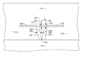
- FIG. 4 is an ABS view of a portion of the magnetic write head of FIG. 3 ;
- FIG. 5 is graph of write field gradient for various magnetic write head configurations at a first side gap length
- FIG. 6 is a graph of fringing field for various magnetic write head configurations at the first side gap length
- FIG. 7 is a graph of negative field for various magnetic write head configurations at the first side gap length
- FIG. 8 is a graph of write field gradient for various magnetic write head configurations at a second side gap length
- FIG. 9 is a graph of fringing field for various magnetic write head configurations at the second side gap length
- FIG. 10 is a graph of negative field for various magnetic write head configurations at the second side gap length
- FIG. 11 is an ABS view of a portion of a write head according to an alternate embodiment of the invention.
- FIG. 12 is a graph of field gradient for various write head configurations including the alternate embodiment of FIG. 11 ;
- FIG. 13 is a graph of fringing field for various write head configurations including the alternate embodiment of FIG. 11 ;
- FIG. 14 is a graph of negative field for various write head configurations including the alternate embodiment of FIG. 11 ;
- FIG. 15 is an ABS view of a portion of a write head according to yet another embodiment of the invention.
- FIG. 16 is a graph of field gradient for various gap extension angles for the embodiment of FIG. 15 ;
- FIGS. 17-25 are views of a write head in various intermediate stages of manufacture, illustrating a method of manufacturing a write head according to an embodiment of the invention.
- FIGS. 26-34 are views of a write head in various intermediate stages of manufacture, illustrating a method of manufacturing a write head according to another embodiment of the invention.
- FIG. 1 there is shown a disk drive 100 embodying this invention.
- at least one rotatable magnetic disk 112 is supported on a spindle 114 and rotated by a disk drive motor 118 .
- the magnetic recording on each disk is in the form of annular patterns of concentric data tracks (not shown) on the magnetic disk 112 .
- At least one slider 113 is positioned near the magnetic disk 112 , each slider 113 supporting one or more magnetic head assemblies 121 . As the magnetic disk rotates, slider 113 moves radially in and out over the disk surface 122 so that the magnetic head assembly 121 may access different tracks of the magnetic disk where desired data are written.
- Each slider 113 is attached to an actuator arm 119 by way of a suspension 115 .
- the suspension 115 provides a slight spring force which biases slider 113 against the disk surface 122 .
- Each actuator arm 119 is attached to an actuator means 127 .
- the actuator means 127 as shown in FIG. 1 may be a voice coil motor (VCM).
- the VCM comprises a coil movable within a fixed magnetic field, the direction and speed of the coil movements being controlled by the motor current signals supplied by controller 129 .
- the rotation of the magnetic disk 112 generates an air bearing between the slider 113 and the disk surface 122 which exerts an upward force or lift on the slider.
- the air bearing thus counter-balances the slight spring force of suspension 115 and supports slider 113 off and slightly, above the disk surface by a small, substantially constant spacing during normal operation.
- control unit 129 The various components of the disk storage system are controlled in operation by control signals generated by control unit 129 , such as access control signals and internal clock signals.
- control unit 129 comprises logic control circuits, storage means and a microprocessor.
- the control unit 129 generates control signals to control various system operations such as drive motor control signals on line 123 and head position and seek control signals on line 128 .
- the control signals on line 128 provide the desired current profiles to optimally move and position slider 113 to the desired data track on disk 112 .
- Write and read signals are communicated to and from write and read heads 121 by way of recording channel 125 .
- FIG. 2 is an ABS view of the slider 113 , and as can be seen the magnetic head including an inductive write head and a read sensor, is located at a trailing edge of the slider.
- the magnetic head including an inductive write head and a read sensor is located at a trailing edge of the slider.
- FIG. 1 The above description of a typical magnetic disk storage system, and the accompanying illustration of FIG. 1 are for representation purposes only. It should be apparent that disk storage systems may contain a large number of disks and actuators, and each actuator may support a number of sliders.
- FIG. 3 is a side cross sectional view of a magnetic write head 300 that can be constructed by a method of the present invention.
- the write head 300 includes a magnetic write pole 302 and a magnetic return pole 304 .
- the magnetic write pole 302 can be connected with a magnetic shaping layer 306 that helps to conduct magnetic flux to the tip of the write pole 302 .
- the write pole 302 and shaping layer 306 can be connected with the magnetic return pole 304 by a magnetic back gap structure 308 .
- a non-magnetic, electrically conductive write coil 310 passes between the return pole 304 and the write pole and shaping layer 302 , 306 , and may also pass above the write pole and shaping layer 302 , 306 .
- the write coil 310 can be encased in a non-magnetic, electrically insulating material 312 , which can be a material such as alumina and/or hard baked photoresist.
- a magnetic field is induced around the coil 310 that results in a magnetic flux flowing through the return pole 304 , back gap layer 308 , shaping layer 306 and write pole 302 .
- This strong, highly concentrated write field locally magnetizes a magnetic top layer 314 of the magnetic media 112 .
- the magnetic field then travels through a soft magnetic under-layer 316 of the magnetic media before returning to the return pole 304 , where it is sufficiently spread out and weak that it does not erase the previously recorded bit of data.
- the write head 300 can also include a magnetic pedestal 305 , at the ABS that acts as a shield to prevent stray fields, such as those from the write coil 310 from reaching the magnetic medium 112 .
- the write head 300 also includes a trailing magnetic shield 318 , located at the air bearing surface (ABS) and separated from the write pole 302 by a non-magnetic trailing gap layer 326 .
- the trailing magnetic shield 318 can be connected with the other magnetic structures at the back of the write head 300 by a trailing magnetic pole 322 .
- FIG. 4 shows a view of the write pole 302 as seen from the Air Bearing Surface (ABS).
- the write pole 302 has a trailing edge 402 , a leading edge 404 , and first and second laterally opposed sides 406 , 408 that each extend from the trailing edge 402 to the leading edge 404 .
- the first and second sides 406 , 408 are preferably tapered so that the write pole 302 is wider at the trailing edge 402 than it is at the leading edge 404 .
- the shield 318 extends down to provide side shield portions 410 , 412 , which are separated from the sides 406 , 408 of the write pole 302 by non-magnetic side gap layers 414 , 416 that define a side gap length (SG).
- the trailing edge 402 of the write pole 302 is separated from the trailing shield 318 by the non-magnetic trailing gap layer 320 , described previously with reference to FIG. 3 that defines a trailing gap length TG.
- the head 300 also includes non-magnetic gap extensions 418 , 420 that extend laterally outward. In the embodiment shown in FIG. 4 these gap extensions extend laterally outward from the trailing gap 320 , and can be considered to be extensions of the trailing gap.
- the gap structure 320 , 418 , 420 includes notches located at the top of the side gaps 414 , 416 . These notches result in first and second convex bump structures 422 , 424 formed in the trailing shield 318 . These convex bump structures 422 , 424 are located near the top (trailing most portion) of the side gaps 414 , 416 and extend in a leading direction as shown. Each of the convex notches has a bump height (BH) measured from the leading edge 422 of the trailing portion of the trailing shield 318 .
- BH bump height
- the side shield portions 410 , 412 further help to prevent adjacent track interference.
- the non-magnetic side gaps 414 , 416 are preferably made thicker than the trailing gap 320 to prevent the loss of write field to the side shield portions 410 , 412 .
- the present invention provides a structure for a recording head that provides a high Signal to Noise Ratio (SNR) in a high data density disk drive device, and also provides method for constructing such a write head, as will be described further below.
- SNR Signal to Noise Ratio
- the presence of the trailing shield 318 achieves the increase in field gradient by attracting magnetic write field toward the trailing edge 402 of the write pole 302 .
- FIGS. 5 , 6 and 7 illustrate the various performance characteristics for various write head structures.
- Each of the graphs of FIGS. 5 , 6 and 7 illustrate such performance characteristics for a write head having a side gap length SG of 60 nm and a trailing shield gap TG of 30 nm, and in the graphs of each of FIGS. 5 , 6 and 7 the location A corresponds to a write head having a bump height BH ( FIG. 4 ) that is equal to 1 ⁇ 2 the trailing gap (TG).
- Location B corresponds to a write head having a bump height (BH) that is equal to the trailing gap (TG).
- Location C represents a write head having no convex bump 422 , 424 ( FIG.
- FIGS. 8 , 9 and 10 are similar to those of FIGS. 5 , 6 and 7 respectively, except that they illustrate the performance characteristics for a write head having a side shield gap of only 30 nm (e.g. equal to the trailing gap).
- FIGS. 5 , 6 and 7 respectively evaluated in FIGS. 5 , 6 and 7 respectively for a write head having a side gap of 60 nm.
- the negative field was reduced (increase in the absolute value) compared with a structure having wing extension 418 , 420 but no convex bump 422 , 424 (corresponding to location C on FIG. 7 ), indicating improved performance.
- FIG. 5 indicates an improvement in average field gradient for a write head having the convex bump (graph locations A and B) compared with a structure having no bump (graph locations C and D).
- the improved performance of the a write head having a convex bump is indicated by the increase in average field gradient with reduced impairment of fringe field and negative magnetic field.
- FIGS. 8 , 9 and 10 show the performance characteristics for a write head wherein the side gap is 30 nm or about equal to the trailing gap. This was done in order to examine the relationship between convex part height and side shield gap. As shown by the results in FIGS. 8 , 9 and 10 , when the convex part height is equal to the trailing gap, the amount of write pole magnetic flux lost to the trailing shield was reduced, and reduction in the negative field was apparent. From the above it can be concluded that the improvements resulting from the present invention are maximized when the height of the convex bump is at least 1 ⁇ 2 of the trailing gap and no more than 1 ⁇ 2 of the side shield gap.
- another embodiment of the invention includes non-magnetic side gap wing extensions 1102 , 1104 that are not located at the trailing gap 320 , but, rather, are located at a location at a level that is between the trailing edge 402 and leading edge 404 of the write pole 302 .
- the non-magnetic side gap wing extensions each have a trailing edge 1106 that is separated from a plane defined by the trailing edge 402 of the write pole 302 by a distance X.
- FIG. 11 The structure of FIG. 11 , wherein the third gap is located between the levels of the leading edge 402 and trailing edge 404 was investigated in an embodiment in which the gap length of 1102 and 1104 (measured vertically in FIG. 11 ) was about equal to the trailing gap length 320 , and wherein the amount of offset X between the level of the leading edge 402 and the location of the wing extensions 1102 , 1104 was 20 or 40 nm.
- FIGS. 12 , 13 and 14 illustrate various performance variables for various write head configuration in order to compare the performance of the write head of FIG. 11 with that of other configurations.
- FIG. 12 shows the Average Field Gradient for various write head configurations.
- FIG. 13 shows the Fringing Field for various write head configurations, and
- FIG. 14 shows the Negative Field for various write head configurations.
- the location A represents the performance of a structure such as that of FIG. 4 .
- Location B represents the performance of a write head having a “T” shaped trailing gap as in FIG. 4 , but with no convex bump structures 422 , 424 .
- Location C represents a write head having a conformal trailing wrap-around shield with no “T” shaped trailing gap and no offset trailing gap.
- Location D represents the performance of a structure such as that of FIG. 11 with an offset X that is equal to the length of the trailing gap 320
- location E represents the performance for a head having an offset X that is equal to two times the length of the trailing gap.
- the trailing gap length was set at 20 nm.
- the field gradient and negative field for a head having an offset was roughly equivalent to that for the structure of FIG. 4 .
- the Fringing Field FIG. 13
- a head having an offset was found to be useful in a range where the fringe field does not exceed the permitted drive values.
- FIG. 15 illustrates yet another possible embodiment of a write head as viewed from the ABS.
- the head of FIG. 15 has side shield gap 1502 , 1504 , and a trailing gap 320 , and has laterally extending, non-magnetic gap wings 506 , 508 , that are angled as shown in FIG. 15 .
- the gap wings 506 , 508 comprise a non-magnetic material such as (for example) alumina, and are formed at an angle ⁇ relative to a plane that is parallel with the trailing edge 402 .
- the Average Field Gradient for a head having various slope angles ⁇ is shown in FIG. 16 .
- the location 1602 is the field gradient for a head such as that of FIG. 4 , having a convex bump 422 , 424 and zero slope angle ⁇ .
- the line 1604 shows the Average Field Gradient in Oe/nm for a head for various wing angles ⁇ for a head having no convex bump 422 , 424 (e.g. the structure of FIG. 15 ).
- the angle ⁇ was varied (without the convex bump), the magnetic field curvature was somewhat improved the greater the angle ⁇ , but as can be seen in FIG. 15 , it deteriorated with increasing average field gradient.
- the gap was “Y” shaped, and as a result, the trailing shield gap length is greater in the region of the track ends.
- the increase in field gradient for a structure as shown in FIG. 4 and FIG. 11 was found to be 15-20 Oe/nm greater than a prior art structure having no convex bump and no wing gap offset.
- the accompanying signal to noise ratio SNR was estimated by Read/Write (RW) calculation using micro-magnetic simulation of current media, the increase in SNR produced by the above mentioned field gradient remained at 0.2-0.3 dB, but with refined media which are currently under development, it is likely that the magnetic particle size of media will be around 7% smaller than that of existing media, and as a result, the SNR gain produced by the increased field gradient will increase and an improvement in SNR of 0.5-0.6 dB can be anticipated.
- the finer the magnetic particle size of the medium the greater the SNR gain produced by the increased field gradient will be, making the inventive head structure even more effective for a high density recording medium.
- FIGS. 17-25 illustrate a method of manufacturing a magnetic write head such as that described above with reference to FIG. 4 .
- a substrate 1702 is provided, which can be a material such as alumina and can also include all or a portion of a magnetic structure such as a shaping layer 306 ( FIG. 3 ).
- a magnetic material 1704 such as NiFe is then deposited over the substrate 1702 .
- the magnetic layer 1704 is deposited to a length that is at least as thick as the height of a write pole to be formed.
- a mask structure 1706 is then formed over the magnetic material 1704 .
- the mask can be a patterned photoresist layer and can include other material layers as well.
- the mask has an opening that is configured to define a write pole.
- a reactive ion etching is performed to remove portions of the magnetic material layer 1704 that are not protected by the mask 1706 , thereby forming a trench as shown in FIG. 18 .
- the reactive ion etching is preferably performed in such a manner as to form a trench with tapered side walls as shown.
- the photoresist can then be lifted off, and a non-magnetic material such as Ru 1902 is deposited by a conformal deposition process such as atomic layer deposition to evenly coat the inside walls of the trench.
- This non-magnetic material 1902 provides a non-magnetic side gap, and also advantageously reduces the track width of the write pole, as will be seen.
- a magnetic material 2002 can then be electroplated into the trench, over the non-magnetic layer 1902 as shown in FIG. 20 .
- the non-magnetic layer 1902 can be used as an electroplating seed.
- a chemical mechanical polishing process can then be performed planarize the structure and to remove portions of the layers 1902 , 2002 that extend outside of the trench.
- a reactive ion etching is then performed to remove a portion of the side gap material 1902 , forming a recess in the top of the layer 1902 .
- This reactive ion etching can be performed in a chemistry that preferentially removes the side gap material at a faster rate than the magnetic material 1704 or 1902 .
- a trailing gap material 2202 such as alumina is deposited to a length of a desired trailing gap as shown in FIG. 22 .
- a mask 2302 is then formed having a width that is chosen to determine the extent to which the trailing gap will extend laterally beyond the write pole 2002 .
- An ion milling or reactive ion etching is then performed to remove portions of the trailing gap layer 2202 that are not protected by the mask 2302 , leaving a structure as shown in FIG. 24 .
- the mask 2302 can then be removed and a trailing shield 2502 can be formed by electroplating a magnetic material such as NiFe.
- FIGS. 26-34 illustrate a method for manufacturing a magnetic write head such as the write head described above with regard to FIG. 11 .
- a substrate 1702 is provided and magnetic material 2602 such as NiFe is deposited over the substrate.
- a layer of RIEable, CMP resistant material such as diamond like carbon (DLC) is deposited over the magnetic material 2602 .
- a mask 2606 is formed over the layer 2604 .
- the mask can be a patterned photoresist mask but can contain other layers as well and has an opening that is configured to define a write pole.
- a material removal process such as ion milling and/or reactive ion etching is performed to remove portions of the layers 2602 , 2604 that are not protected by the mask 2606 , leaving a structure as shown in FIG. 27 .
- the mask 2606 can then be lifted off, and a non-magnetic, electrically conductive material such as Ru can be conformally deposited, leaving a structure such as that shown in FIG. 28 .
- a magnetic material 2902 can then be deposited by electroplating, leaving a structure such as that shown in FIG. 29 . This can be followed by a chemical mechanical polishing process that removes portions of the layers 2802 and 2902 that extend out of the trench.
- the CMP is terminated at the layer 2604 , which as mentioned above is a CMP resistant material. This leaves a structure as shown in FIG. 30 .
- a reactive ion etching can be performed to remove the remaining layer 2604 , leaving a structure as shown in FIG. 31 , with the write pole 2902 and non-magnetic side gap layers 2802 extending out of the top of the magnetic material 2602 .
- a non-magnetic trailing gap material layer 3202 is deposited to a length that is chosen to define a trailing gap.
- a mask 3302 is formed over the structure, the mask 3302 having a width that will determine the amount by which the trailing gap layer 3202 extends laterally from the write pole and side gap layers 2802 .
- a quick reactive ion etching or on milling is then performed to remove portions of the trailing gap layer 3202 that extend beyond the mask 3302 .
- a trailing magnetic shield 3402 can then be formed by electroplating a material such as NiFe, leaving a structure such as that shown in FIG. 34 .
- extending side portions of the gap layer 3202 are offset by a distance X. This amount of this offset X is determined by the layer 2604 , the deposition of which was described above with reference to FIG. 26 .
Abstract
Description
Claims (19)
Priority Applications (1)
| Application Number | Priority Date | Filing Date | Title |
|---|---|---|---|
| US13/294,816 US8630064B2 (en) | 2011-11-11 | 2011-11-11 | Magnetic write head with novel shield structure having latterally extending trailing gap layer and concaved side gap |
Applications Claiming Priority (1)
| Application Number | Priority Date | Filing Date | Title |
|---|---|---|---|
| US13/294,816 US8630064B2 (en) | 2011-11-11 | 2011-11-11 | Magnetic write head with novel shield structure having latterally extending trailing gap layer and concaved side gap |
Publications (2)
| Publication Number | Publication Date |
|---|---|
| US20130120876A1 US20130120876A1 (en) | 2013-05-16 |
| US8630064B2 true US8630064B2 (en) | 2014-01-14 |
Family
ID=48280412
Family Applications (1)
| Application Number | Title | Priority Date | Filing Date |
|---|---|---|---|
| US13/294,816 Active 2032-03-22 US8630064B2 (en) | 2011-11-11 | 2011-11-11 | Magnetic write head with novel shield structure having latterally extending trailing gap layer and concaved side gap |
Country Status (1)
| Country | Link |
|---|---|
| US (1) | US8630064B2 (en) |
Cited By (3)
| Publication number | Priority date | Publication date | Assignee | Title |
|---|---|---|---|---|
| US8947828B1 (en) * | 2014-03-18 | 2015-02-03 | HGST Netherlands B.V. | Magnetic head having a double bump wrap around shield |
| US8988824B1 (en) * | 2013-12-23 | 2015-03-24 | HGST Netherlands B.V. | Method for manufacturing a magnetic write pole with a consistent bevel angle |
| US20160035374A1 (en) * | 2014-07-30 | 2016-02-04 | Kabushiki Kaisha Toshiba | Magnetic recording head and magnetic recording and reproducing device |
Families Citing this family (2)
| Publication number | Priority date | Publication date | Assignee | Title |
|---|---|---|---|---|
| US9269378B2 (en) | 2013-12-20 | 2016-02-23 | HGST Netherlands B.V. | Stray field shielding for perpendicular magnetic recording write head |
| US9805753B2 (en) * | 2016-03-23 | 2017-10-31 | Western Digital Technologies, Inc. | Enhanced write pole and return pole for improved areal density |
Citations (22)
| Publication number | Priority date | Publication date | Assignee | Title |
|---|---|---|---|---|
| US20050219764A1 (en) * | 2004-03-31 | 2005-10-06 | Alps Electric Co., Ltd. | Perpendicular magnetic recording head and method of manufacturing the same |
| US20070115584A1 (en) | 2005-11-23 | 2007-05-24 | Hitachi Global Storage Technologies | Write head design and method for reducing adjacent track interference in at very narrow track widths |
| US7239478B1 (en) | 2004-01-31 | 2007-07-03 | Western Digital (Fremont), Inc. | Write element for perpendicular recording in a data storage system |
| US20080068747A1 (en) * | 2006-09-11 | 2008-03-20 | Headway Technologies, Inc. | Magnetic head for perpendicular magnetic recording and method of manufacturing same |
| US20080278861A1 (en) | 2007-05-11 | 2008-11-13 | Ming Jiang | Stitched wrap around shield fabrication for perpendicular magnetic recording write heads |
| US7467461B2 (en) | 2007-03-20 | 2008-12-23 | Hitachi Global Storage Technologies Netherlands B.V. | Additive gap process to define trailing and side shield gap for a perpendicular write head |
| US7551396B2 (en) | 2005-04-27 | 2009-06-23 | Hitachi Global Storage Technologies Netherlands B.V. | Perpendicular magnetic write head having a studded trailing shield compatible with read/write offset |
| US20090168240A1 (en) | 2007-12-28 | 2009-07-02 | Wen-Chien David Hsiao | Perpendicular write head having a modified wrap-around shield to improve overwrite, adjacent track interference and magnetic core width dependence on skew angle |
| US7609479B2 (en) | 2006-03-10 | 2009-10-27 | Headway Technologies, Inc. | Magnetic head for perpendicular magnetic recording and method of manufacturing same |
| US20100007996A1 (en) | 2008-06-19 | 2010-01-14 | Kabushiki Kaisha Toshiba | Magnetic head assembly and magnetic recording/reproducing apparatus |
| US7712206B2 (en) | 2006-05-22 | 2010-05-11 | Hitachi Global Storage Technologies Netherlands B.V. | Method for manufacturing a magnetic write head having a trailing shield with an accurately controlled trailing shield gap thickness |
| JP2010108533A (en) | 2008-10-28 | 2010-05-13 | Toshiba Storage Device Corp | Magnetic recording head and storage device |
| US20100157472A1 (en) | 2008-12-24 | 2010-06-24 | Wen-Chien David Hsiao | Magnetic write head having a self-aligned side wrap-around shield with multi-angle slanted bump |
| US20100188783A1 (en) | 2009-01-27 | 2010-07-29 | Kabushiki Kaisha Toshiba | Magnetic head, and disk apparatus having the same |
| US20100302680A1 (en) | 2009-06-01 | 2010-12-02 | Tdk Corporation | Perpendicular magnetic write head and magnetic write device |
| US20100321835A1 (en) | 2009-06-22 | 2010-12-23 | Seagate Technology Llc | Self-aligned, trailing edge partial side shield and method of making |
| US7869160B1 (en) | 2005-04-27 | 2011-01-11 | Western Digital (Fremont), Llc | Perpendicular recording head with shaped pole surfaces for higher linear data densities |
| US20110007428A1 (en) | 2009-07-13 | 2011-01-13 | Seagate Technology Llc | Write pole with a synthesized low magnetization shield |
| US20110146062A1 (en) * | 2009-12-17 | 2011-06-23 | Allen Donald G | Method for manufacturing a magnetic write head having a wrap around shield that is magnetically coupled with a leading magnetic shield |
| US20110205671A1 (en) * | 2010-02-23 | 2011-08-25 | Seagate Technology Llc | Magnetic recording head with notched shield |
| US20120281314A1 (en) * | 2011-05-04 | 2012-11-08 | Seagate Technology Llc | Magnetic Shield with Flux Concentration Feature |
| US8347489B2 (en) * | 2010-09-01 | 2013-01-08 | Hitachi Global Storage Technologies Netherlands B.V. | Method for manufacturing a perpendicular magnetic write head having a leading edge tapered write pole, self aligned side shield and independent trailing shield |
-
2011
- 2011-11-11 US US13/294,816 patent/US8630064B2/en active Active
Patent Citations (23)
| Publication number | Priority date | Publication date | Assignee | Title |
|---|---|---|---|---|
| US7239478B1 (en) | 2004-01-31 | 2007-07-03 | Western Digital (Fremont), Inc. | Write element for perpendicular recording in a data storage system |
| US20050219764A1 (en) * | 2004-03-31 | 2005-10-06 | Alps Electric Co., Ltd. | Perpendicular magnetic recording head and method of manufacturing the same |
| US7869160B1 (en) | 2005-04-27 | 2011-01-11 | Western Digital (Fremont), Llc | Perpendicular recording head with shaped pole surfaces for higher linear data densities |
| US7551396B2 (en) | 2005-04-27 | 2009-06-23 | Hitachi Global Storage Technologies Netherlands B.V. | Perpendicular magnetic write head having a studded trailing shield compatible with read/write offset |
| US20070115584A1 (en) | 2005-11-23 | 2007-05-24 | Hitachi Global Storage Technologies | Write head design and method for reducing adjacent track interference in at very narrow track widths |
| US7609479B2 (en) | 2006-03-10 | 2009-10-27 | Headway Technologies, Inc. | Magnetic head for perpendicular magnetic recording and method of manufacturing same |
| US7712206B2 (en) | 2006-05-22 | 2010-05-11 | Hitachi Global Storage Technologies Netherlands B.V. | Method for manufacturing a magnetic write head having a trailing shield with an accurately controlled trailing shield gap thickness |
| US20080068747A1 (en) * | 2006-09-11 | 2008-03-20 | Headway Technologies, Inc. | Magnetic head for perpendicular magnetic recording and method of manufacturing same |
| US7467461B2 (en) | 2007-03-20 | 2008-12-23 | Hitachi Global Storage Technologies Netherlands B.V. | Additive gap process to define trailing and side shield gap for a perpendicular write head |
| US20080278861A1 (en) | 2007-05-11 | 2008-11-13 | Ming Jiang | Stitched wrap around shield fabrication for perpendicular magnetic recording write heads |
| US20090168240A1 (en) | 2007-12-28 | 2009-07-02 | Wen-Chien David Hsiao | Perpendicular write head having a modified wrap-around shield to improve overwrite, adjacent track interference and magnetic core width dependence on skew angle |
| US20100007996A1 (en) | 2008-06-19 | 2010-01-14 | Kabushiki Kaisha Toshiba | Magnetic head assembly and magnetic recording/reproducing apparatus |
| JP2010108533A (en) | 2008-10-28 | 2010-05-13 | Toshiba Storage Device Corp | Magnetic recording head and storage device |
| US20100157472A1 (en) | 2008-12-24 | 2010-06-24 | Wen-Chien David Hsiao | Magnetic write head having a self-aligned side wrap-around shield with multi-angle slanted bump |
| US20100188783A1 (en) | 2009-01-27 | 2010-07-29 | Kabushiki Kaisha Toshiba | Magnetic head, and disk apparatus having the same |
| JP2010176732A (en) | 2009-01-27 | 2010-08-12 | Toshiba Corp | Magnetic head and disk apparatus having the same |
| US20100302680A1 (en) | 2009-06-01 | 2010-12-02 | Tdk Corporation | Perpendicular magnetic write head and magnetic write device |
| US20100321835A1 (en) | 2009-06-22 | 2010-12-23 | Seagate Technology Llc | Self-aligned, trailing edge partial side shield and method of making |
| US20110007428A1 (en) | 2009-07-13 | 2011-01-13 | Seagate Technology Llc | Write pole with a synthesized low magnetization shield |
| US20110146062A1 (en) * | 2009-12-17 | 2011-06-23 | Allen Donald G | Method for manufacturing a magnetic write head having a wrap around shield that is magnetically coupled with a leading magnetic shield |
| US20110205671A1 (en) * | 2010-02-23 | 2011-08-25 | Seagate Technology Llc | Magnetic recording head with notched shield |
| US8347489B2 (en) * | 2010-09-01 | 2013-01-08 | Hitachi Global Storage Technologies Netherlands B.V. | Method for manufacturing a perpendicular magnetic write head having a leading edge tapered write pole, self aligned side shield and independent trailing shield |
| US20120281314A1 (en) * | 2011-05-04 | 2012-11-08 | Seagate Technology Llc | Magnetic Shield with Flux Concentration Feature |
Cited By (4)
| Publication number | Priority date | Publication date | Assignee | Title |
|---|---|---|---|---|
| US8988824B1 (en) * | 2013-12-23 | 2015-03-24 | HGST Netherlands B.V. | Method for manufacturing a magnetic write pole with a consistent bevel angle |
| US8947828B1 (en) * | 2014-03-18 | 2015-02-03 | HGST Netherlands B.V. | Magnetic head having a double bump wrap around shield |
| US20160035374A1 (en) * | 2014-07-30 | 2016-02-04 | Kabushiki Kaisha Toshiba | Magnetic recording head and magnetic recording and reproducing device |
| US9697853B2 (en) | 2014-07-30 | 2017-07-04 | Kabushiki Kaisha Toshiba | Magnetic recording head and magnetic recording and reproducing device |
Also Published As
| Publication number | Publication date |
|---|---|
| US20130120876A1 (en) | 2013-05-16 |
Similar Documents
| Publication | Publication Date | Title |
|---|---|---|
| US8068312B2 (en) | Perpendicular magnetic write head with stitched notched trailing shield | |
| US7715147B2 (en) | Magnetic write head having a shield that extends below the leading edge of the write pole | |
| US8066892B2 (en) | Method for manufacturing a perpendicular magnetic write head with a wrap around shield | |
| US8000059B2 (en) | Perpendicular magnetic write head with a thin wrap around magnetic shield | |
| US7969684B2 (en) | Write head design and method for reducing adjacent track interference at very narrow track widths | |
| US8570686B2 (en) | Magnetic recording head with non-conformal side shield gap | |
| US8323727B2 (en) | Method for manufacturing a perpendicular magnetic write head having a tapered write pole and a stepped wrap around side shield gap | |
| US7515381B2 (en) | Method for fabricating a side shield for a flux guide layer for perpendicular magnetic recording | |
| US7551396B2 (en) | Perpendicular magnetic write head having a studded trailing shield compatible with read/write offset | |
| US8201320B2 (en) | Method for manufacturing a magnetic write head having a wrap around shield that is magnetically coupled with a leading magnetic shield | |
| US7612963B2 (en) | Perpendicular magnetic recording head with photoresist dam between write coil and air bearing surface | |
| US8339734B2 (en) | Magnetic write head having a wrap around trailing shield with an asymetrical side gap | |
| US7712206B2 (en) | Method for manufacturing a magnetic write head having a trailing shield with an accurately controlled trailing shield gap thickness | |
| US8189292B2 (en) | Method for manufacturing a magnetic write head having a write pole with a trailing edge taper using a Rieable hard mask | |
| US7990651B2 (en) | Method of manufacturing a perpendicular magnetic write head with stepped trailing magnetic shield with electrical lapping guide control | |
| US8451562B2 (en) | Method for manufacturing a magnetic write head having a wrap around trailing magnetic shield with a tapered side gap | |
| US8268407B2 (en) | Method for manufacturing a perpendicular magnetic write head having write pole | |
| US8630064B2 (en) | Magnetic write head with novel shield structure having latterally extending trailing gap layer and concaved side gap | |
| US20090255899A1 (en) | Additive write pole process for wrap around shield | |
| US20100155364A1 (en) | Magnetic write head having a stepped trailing shield and write pole with a sloped trailing edge | |
| US7523550B2 (en) | Process to open connection vias on a planarized surface | |
| US8349197B2 (en) | Method for manufacturing a perpendicular magnetic write head having a tapered write pole and non-magnetic bump structure | |
| US8031434B2 (en) | Hybrid, self aligned magnetic write head with a partially plated pole and method of producing same | |
| US8371019B1 (en) | Method for manufacturing a magnetic write pole having straight side walls and a well defined track-width | |
| US8318031B2 (en) | Method for manufacturing a perpendicular magnetic write head having a tapered write pole |
Legal Events
| Date | Code | Title | Description |
|---|---|---|---|
| AS | Assignment |
Owner name: HITACHI GLOBAL STORAGE TECHNOLOGIES NETHERLANDS B. Free format text: ASSIGNMENT OF ASSIGNORS INTEREST;ASSIGNORS:MAEDA, MAKI;ETO, KIMITOSHI;SHIINA, HIROMI;AND OTHERS;SIGNING DATES FROM 20110111 TO 20111026;REEL/FRAME:027700/0450 |
|
| AS | Assignment |
Owner name: HGST NETHERLANDS B.V., NETHERLANDS Free format text: CHANGE OF NAME;ASSIGNOR:HITACHI GLOBAL STORAGE TECHNOLOGIES NETHERLANDS B.V.;REEL/FRAME:029341/0777 Effective date: 20120723 |
|
| FEPP | Fee payment procedure |
Free format text: PAYOR NUMBER ASSIGNED (ORIGINAL EVENT CODE: ASPN); ENTITY STATUS OF PATENT OWNER: LARGE ENTITY |
|
| STCF | Information on status: patent grant |
Free format text: PATENTED CASE |
|
| CC | Certificate of correction | ||
| AS | Assignment |
Owner name: WESTERN DIGITAL TECHNOLOGIES, INC., CALIFORNIA Free format text: ASSIGNMENT OF ASSIGNORS INTEREST;ASSIGNOR:HGST NETHERLANDS B.V.;REEL/FRAME:040826/0327 Effective date: 20160831 |
|
| FPAY | Fee payment |
Year of fee payment: 4 |
|
| AS | Assignment |
Owner name: JPMORGAN CHASE BANK, N.A., AS AGENT, ILLINOIS Free format text: SECURITY INTEREST;ASSIGNOR:WESTERN DIGITAL TECHNOLOGIES, INC.;REEL/FRAME:052915/0566 Effective date: 20200113 |
|
| MAFP | Maintenance fee payment |
Free format text: PAYMENT OF MAINTENANCE FEE, 8TH YEAR, LARGE ENTITY (ORIGINAL EVENT CODE: M1552); ENTITY STATUS OF PATENT OWNER: LARGE ENTITY Year of fee payment: 8 |
|
| AS | Assignment |
Owner name: WESTERN DIGITAL TECHNOLOGIES, INC., CALIFORNIA Free format text: RELEASE OF SECURITY INTEREST AT REEL 052915 FRAME 0566;ASSIGNOR:JPMORGAN CHASE BANK, N.A.;REEL/FRAME:059127/0001 Effective date: 20220203 |
|
| AS | Assignment |
Owner name: JPMORGAN CHASE BANK, N.A., ILLINOIS Free format text: PATENT COLLATERAL AGREEMENT - A&R LOAN AGREEMENT;ASSIGNOR:WESTERN DIGITAL TECHNOLOGIES, INC.;REEL/FRAME:064715/0001 Effective date: 20230818 |